How Do you Do Mounting Circuit Boards ?

A Step-by-Step Guide to Mounting Circuit Boards

Circuit boards, also known as printed circuit boards (PCBs), are thin boards that hold chips and other electronic components. Properly mounting circuit boards is crucial for building electronic devices that function correctly. This guide will walk you through the key steps for securely mounting circuit boards in your projects.

Gather Your Materials

You will need the following materials:

  • Circuit board
  • Standoffs
  • Screws
  • Nuts and washers
  • Mounting brackets (optional)
  • Soldering iron and solder
  • Wire cutters/strippers
  • Multimeter

Make sure to choose hardware designed for mounting circuit boards such as nylon or brass standoffs. You’ll also want screws that fit through the mounting holes on your circuit board.

Prepare the Enclosure

First, plan where your circuit board will be positioned inside the enclosure. Clean the area thoroughly to remove any debris. Insert standoffs into the chosen mounting points and twist them in place by hand or use a wrench to fully tighten them.

Position them according to the circuit board holes so the board will align properly when placed. Having standoffs already secured in the case makes mounting easier.

Modify the Board (If Needed)

Some modifications may be required to mount the board securely:

  • Cut traces on the solder side to disconnect ground planes going to mounting holes. This prevents short circuits.
  • Drill new holes if the existing ones don’t line up with your standoffs. Place tape over the area first to prevent cracking.

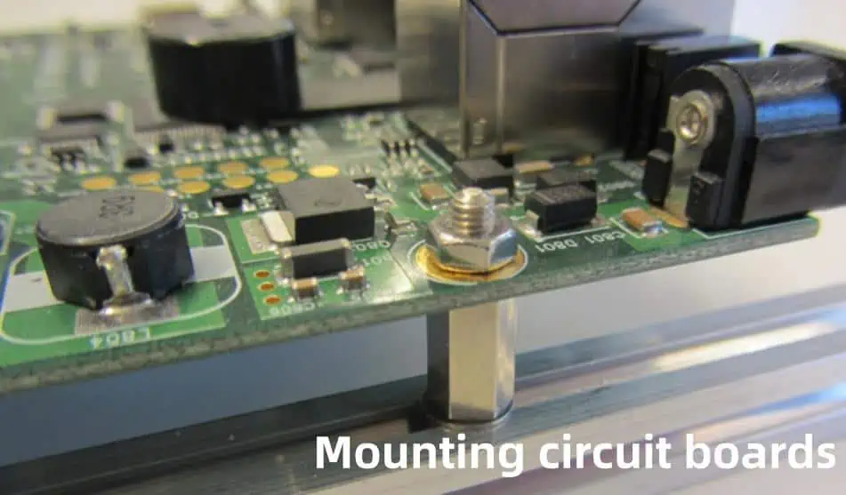
Attach Mounting Hardware

With the standoffs inserted into the enclosure, carefully place the board onto them, lining up the holes. The standoffs should hold the weight easily without flexing.

On the component side of the board, add a washer and nut onto each protruding standoff screw. Tighten down gently using your fingers first then finish with a wrench. Don’t over tighten or you may damage the board. Ensure the board sits evenly without bending.

Mounting Options:

  • Standoffs and screws – Simple yet secure method. Allows access to both sides of the board.
  • Adhesive mounting pads – Easy option for lightweight boards. Allows you to mount to irregular surfaces.
  • Mounting brackets – Good for larger boards. Brace along the edges with brackets screwed into place.

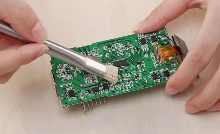
Solder Components and Connections

With the board physically mounted, you can now solder components onto it and make wiring connections:

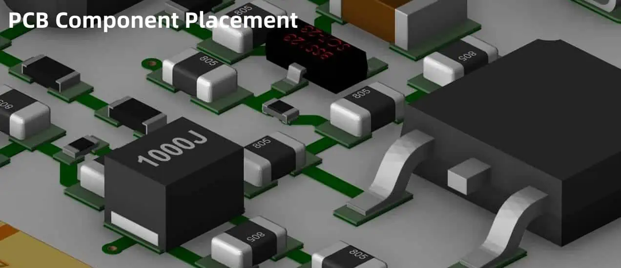
  • Solder components like ICs, capacitors, etc. onto the topside according to circuit diagram
  • Trim excess leads after soldering each component
  • Heatshrink wire connections to prevent shorts
  • Use cable clamps or ties to neatly route wires

Double check your solder connections with a multimeter for quality. Faulty joints can cause problems. Reflow any suspicious ones.

Test and Troubleshoot

Before closing up the enclosure, power up the board and test operation. Observe voltage levels, clock signals or other outputs to verify functionality. The data sheet is key for determining expected results.

If issues are found:

  • Check power connections and polarity first
  • Inspect solder joints under a magnifier for bridging or cold joints
  • Probe test points to verify chip inputs/outputs
  • Swap suspect components like ICs with known working ones
  • Consult board schematics regarding circuit operation

Thorough troubleshooting at this stage prevents headaches later.

Complete Assembly

Once fully functional, finish up by neatly dressing any loose wires with ties, foam, or brackets to prevent wire movement stress. Double check screws and standoffs to ensure they are snugly tightened. Verify clearance space around the board for air ventilation if high-power.

Close up the enclosure, attach connectors, and do final validation tests. Your professionally mounted circuit board is complete! Power up and enjoy your creation.

Pro Tips for Mounting Boards

Here are some expert recommendations for flawlessly mounting PCBs:

Use plastic standoffs – Nylon or polycarbonate standoffs insulate the board from the enclosure versus metallic types. This helps prevent stray Ground paths or short circuits through chassis contacts.

Avoid torque twisting – Uneven tightening of mounting screws can warp the board which strains solder joints. Tighten opposing corner screws gradually to maintain even pressure.

Mount sensibly sized boards – Overly large boards can flex and crack under their own weight without proper support. Use mounting holes evenly spaced across the PCB or structural reinforcement.

Allow ventilation space – Leave clearance between high power boards and enclosure walls for airflow convection cooling. This prevents overheating damage.

Conformal coat when necessary – For boards in harsh environments, apply acrylic coating to shield against moisture corrosion or dust contamination.

Use mounting templates – For production assemblies, laser cut acrylic templates allow consistent hole alignment when positioning boards prior to screwing down.

Paying attention to these professional tips will help your mounted boards function reliably for years of service.

Common Mounting Methods

There are several standard techniques for securing a PCB depending on the intended application:

MethodDescription
StandoffsSeparate cylindrical supports that screw into case
RisersCard-edge connectors allow stacking multiple boards
Rack slidesFor larger chassis with shelf-like card guides
Adhesive padsDouble-sided foam tape bonds board temporarily
Edge clipsMetal brackets that grip the board perimeter
Angled slotsOblique case cuts support PCB edges
Face platesPanel-mounted IO ports hold board from front side

Selecting Proper Standoff Type

Choosing ideal standoffs is key for robust yet simple mounting. Variables that influence the selection:

ConsiderationOptions
Board thickness1-6 mm standoff lengths available
Board heightStandoffs from 1/4 to 2+ inches tall
Number of boardsSingle or multi-stacking standoff types
MaterialNylon, brass, aluminum, stainless steel
Screw typeMatching threads for case material
Hex or Phillips driveDrive style for accessing screw heads

Nylon and brass are common cost-effective options suitable for most applications.

Troubleshooting Mounting Problems

Despite best efforts, you may encounter issues getting a board securely mounted such as:

ProblemLikely CausesSolutions
Board doesn’t align with standoffsEnclosure tolerance variationUse slotted holes, shims, extra washers
Board loose with playLoose screws, stripped threadsUse next screw size up, add washers
Components make contactTall parts touch coverRaise standoffs, double check layout
Unable to access component sideClose proximity to chassisUse only low-profile nuts, risers
Circuit fails intermittentlyThermal cycling moves boardConformal coating, vibration damping

Careful inspection of the actual assembly and planning ahead for mechanical clearance helps mitigate problems. Having standard troubleshooting steps in mind allows you to methodically isolate and remedy mounting-related issues so your board operates reliably.

Mounting Boards in Practice

Here are some examples of mounted boards seen in real electronic products:

ApplicationMounting Method
Desktop PCsVertical riser cards and large cross braces
Set-top cable boxesSmall standoffs epoxied directly to plastic enclosure
Rackmount serversShelf-like horizontal card guides with injection levers
Network switchesFaraday-cage aluminum cases, edge tab mounts
Handheld devicesMiniature boards fixed in place with globs of silicone

Mass-manufactured products utilize optimized, automated mounting techniques tailored closely to the particular board, case, and operating environment. But small-scale projects can achieve similar robust results with mindful part choices and manual installation precision.

Mounting Factors

What determines how a printed circuit board gets mounted?

  • Vibration/shock – Will product move around?
  • Thermal – Does circuit dissipate much heat?
  • EMI/RFI – Plastic standoffs or metal cage?
  • Access – Need to remove easily?
  • Volume – Manual or automated process?
  • Aesthetics – Visible or hidden board?

Analyzing key aspects like these helps dictate ideal mounting methods per application.

FAQ

What are some main advantages of standoffs?

Standoffs securely space boards off conductive enclosure surfaces. They dissipate heat better, allow washers for uniform screw pressure, permit component clearance, and simplify wiring access underneath. Standoffs are affordable and don’t require special tools.

What screw size should I use?

Match screw diameters to mounting hole sizes, allowing 0.5 mm extra clearance. Standard hole sizes are 2.5 mm, 3 mm, and 3.5 mm in most PCBs. Screw lengths depends on stacked board height plus 20-50% extra for safety. Too long and screws bottom out. Too short and threads don’t catch.

Is epoxy a durable mounting method?

Structural epoxies bond well but allow little shear strength, flexibility against vibration, or heat transfer for cooling. Epoxies work only with very lightweight boards. Use reinforced epoxy gel for increased strength. But fasteners permit easier component access and board removal.

What are clearance requirements around boards?

Leave at least 3 mm spacing from enclosure walls and tall components to allow some air circulation. High power circuits require greater clearance or fans. Carefully measure height of tallest elements like capacitors to ensure sufficient headroom when the lid closes.

How can I prevent loose screw connections?

Use threadlocker adhesive so screws resist backing out over time. Split lock washers also fight loosening but add height. When screws won’t grab sufficiently even with washers, replace the standoffs or case threaded holes with next larger size up.

Conclusion

Mounting a printed circuit board properly involves planning enclosure integration details plus allowing maintenance access and expansion capacity. Carefully installing standoffs or other mechanical supports ensures the board remains fixed securely during shipping or operation. Troubleshooting both solder connections and physical mounting integrity prevents erratic failures.

With mindful material selection and methodical fastening techniques, you can achieve dependable mounting of your custom circuit board for years of reliable functionality.

What are SAP and mSAP in Flexible Circuit Fabrication

msap pcb A flexible circuit, also known as a flex circuit or flex PCB, is a type of printed circuit board (PCB) made from flexible insulating substrate materials such as polyimide or polyester. The conductive pathways in a flex circuit are made from metallic materials like copper foil that allow the board to bend and flex without damage.

Flexible circuits are widely used in electronics when flexibility, space savings, or durability are required. Common applications include consumer electronics, medical devices, industrial controls, aerospace, and military systems.

Compared to rigid PCBs, flexible circuits provide advantages like:

  • Ability to bend and flex to fit products with dynamic or tight spaces
  • Resistance to vibration and mechanical stresses
  • Lightweight and thin profile saving space
  • Design freedom for three-dimensional wiring paths
  • Easy assembly by crimping or soldering

What is SAP in Flex Circuits?

SAP stands for “sintered silver adhesive paste” and refers to a conductive paste material used to form interconnects in flexible PCB manufacturing.

The SAP paste consists of silver flakes or micro-particles combined with a polymer adhesive binder. Unlike conductive inks, SAP relies on a post-print heat sintering process which fuses the silver particles together to achieve metal-like electrical conductivity while retaining adhesive bonding properties.

Benefits of SAP

Compared to other flex circuit interconnection methods, SAP offers several advantages:

  • Simplified Processing: SAP eliminates the need for etching, plating, stripping and other chemical processing steps used in traditional PCB fabrication. It allows direct printing of circuits.
  • Fine Pitch Capability: With modern printing techniques, SAP enables fine line and space circuits down to around 100 micron width โ€“ matching or exceeding whatโ€™s achievable with etched copper.
  • Flexibility & Stretchability: Properly designed SAP interconnects remain electrically conductive even when flexing or moderately elongating the circuit material. This helps meet dynamic bending requirements.
  • Thin and Lightweight Circuits: Lack of copper makes SAP-based flex circuits thinner and lighter in weight than traditional flexible PCBs.
  • Adhesive Bonding: SAP provides electrical conductivity and mechanical bond strength in one material. This ensures reliable connections between circuit layers after heat bonding.

In short, sintered silver adhesive paste provides a simplified additive fabrication process for cost-effective flexible PCBs suitable for high bend radius dynamic applications.

SAP Printing Methods

There are several printing methods used to selectively apply SAP onto flexible substrates for circuit patterning:

Inkjet Printing

Uses piezoelectric or thermal inkjet heads to digitally print small silver ink droplets. High resolution but lower throughput.

Aerosol Jet Printing

In this additive method, an aerosol mist of SAP โ€œinkโ€ is focused into patterns by gas flow through a print head nozzle. Allows very fine feature printing.

Screen Printing

A simple thick film printing process involving forcing paste through a patterned mesh screen using a squeegee. Low cost but limited in resolution.

Stencil Printing

Similar to screen printing but uses laser cut metal stencils and automated squeegee to define print patterns. Offers good repeatability and higher density traces.

After printing, the SAP patterns go through a curing step where heat is applied to โ€œsinterโ€ the silver particles, removing binders and adhesives while fusing the metal particles into a conductive structure.

What is mSAP for Flexible Circuits?

mSAP or โ€œmodified silver adhesive pasteโ€ is an advancement over the basic SAP technology for flex PCB fabrication.

The โ€œmodifiedโ€ reference indicates the SAP paste is blended with small amounts of solder powder alloy before sintering.

Typical mSAP alloys contain around 2% tin/bismuth or indium solder powder. Adding these specialty metal alloy powders achieves key benefits:

Lower Sintering Temperature

The alloy modifiers in mSAP paste serve as a fluxing agent during heat curing. This promotes silver particle sintering at lower peak temperatures compared to un-modified SAP.

Typical mSAP sintering happens around 200ยฐC versus 280ยฐC for standard SAP.

Lower thermal budgets are especially important for thin, thermally sensitive flexible circuit substrates. It prevents warping or damage.

Stronger Adhesion

The metal alloy powders alter surface chemistry which subsequently enables superior adhesive bonding of mSAP traces to the flexible substrate.

Standard SAP traces often suffer from weak links at the adhesive interface which then requires additional adhesion promoting coatings or primers.

Improved Flexibility & Crease Durability

Besides lowering the curing temperature, the metal particle modification improves mechanical properties of the sintered mSAP traces.

Specifically, minor alloying introduces more plastic deformation capability. This increases flex life and prevents cracking of circuits when dynamically bending or folding.

In short, mSAP modification allows conductive silver adhesive pastes to achieve better performance metrics crucial for reliable flexible PCB fabrication and functional performance.

Typical mSAP Composition

msap pcb While specific formulations vary between material suppliers, typical second-generation mSAP pastes comprise:

Silver (Ag) 85-90 wt.% โ€“ Flake or spherical microparticle powder providing electrical conductivity.

Alloy Modifier (SnBi or In) 2-5 wt.% โ€“ Specialty indium or tin/bismuth solders to enhance sintering and adhesion.

Organic Binders 5-10 wt.% โ€“ Polymers that assist viscosity control and layer bonding during processing. Burn out when curing.

Solvents 1-5 wt.% โ€“ Carrier liquids like glycols controlling ink rheology for printing.

When printed, the mSAP inks behave similar to SAP during heat exposure:

  1. Solvents evaporate when initially heated
  2. Binders and other organics burn-off next
  3. Finally alloying and sintering fuses silver particles into a conductive structure bonded to the substrate.

Carefully balancing the multi-component paste chemistry enables high performance stretchable conductive traces using simplified low-cost production methods.

mSAP vs Copper Circuits for Flex PCBs

Comparing mSAP to conventionally etched copper flex circuits reveals some key pros and cons influencing usage:

mSAP Advantages

  • Simpler & Lower Additive Process Costs
  • Fine Pitch to 0.1mm with Stencil/Screen Printing
  • Thinner and Lighter Weight
  • Dynamic Flexibility & Folding
  • Strong Adhesion to Base Materials
  • Compatible with Low Temperature & Heat Sensitive Substrates

Copper Advantages

  • Lower Electrical Resistivity
  • Higher Current Carrying Capacity
  • Matched Coefficients of Thermal Expansion
  • Established Complex Circuit & Via Structure Capability
  • Compatible with Surface Finishes (OSP, ENIG, Immersion Tin)

In basic terms, mSAP flex circuits compete well when:

  • Lightweight and thinner profiles are valued
  • Mission profiles involve dynamic bending motions
  • Heat exposure is restricted
  • Cost reduction is needed

Meanwhile, copper circuits remain favored for:

  • High density circuits with smallest features
  • High power or current flow is required
  • Thermal management is a priority
  • Interconnection with standard SMT components

Many applications take a โ€œhybridโ€ approach with mSAP used selectively, like for dynamic interconnects, while copper wiring handles power delivery and component pads.

mSAP Flex Circuit Materials

A wide range of thin insulating substrate materials are used as foundations for mSAP flex PCBs. Popular options include:

Polyimide (PI) films โ€“ This class of polymer offers very high heat resistance along with mechanical strength. Branded versions like DuPont Kapton polyimide film have become synonymous with flex circuits.

Polyethylene Naphthalate (PEN) โ€“ Related to PET but with improved temperature resistance. Allows lower cost than polyimide.

Polyethylene Terephthalate (PET) โ€“ Known by brands like Mylar, PET offers the lowest cost polymer film substrate, but with lower thermal capability than PI or PEN.

Polymide Coated Copper (PCC) โ€“ Uses cast polyimide resin pre-applied to copper foil. This gives a built-in flex circuit substrate with conductive layers ready for patterning.

LCP Blends – Liquid crystal polymer composites tailored for flex circuit fabrication. Combines ease of processing with good electrical and temperature performance.

When combined with thin polymer substrates, mSAP conductive traces measure below 0.1mm total thickness. This enables many new lightweight and compact electronic device designs not possible previously.

mSAP vs Conductive Inks

While both sintered silver technology like mSAP and traditional silver conductive inks rely on silver particulate mixtures, the performance differ significantly:

Silver Inks depend on inert carriers and charge-stabilized chemistry to prevent aggregation. This limits overall silver flake content (~45%) and final conductivity (50X bulk silver).

In contrast, mSAP pastes use alloying and a binder system to achieve 85-90% silver loading and around 5-10X bulk resistivity after sintering.

Furthermore, inks only achieve conductivity through particle contact points within the cured ink film. No fusing or โ€œweldingโ€ together occurs. This means ink traces are mechanically weak and lose connectivity when stretched or bent excessively.

Meanwhile, mSAP traces undergo full sintering to fuse together the nano/micro-silver particles. This generates 10X higher adhesion strength and allows flexibility without electrical failure.

When evaluating electrical conductors for dynamic flexible circuits, mSAP clearly outperforms older silver ink technology on critical performance metrics like conductivity, flexibility and bend life.

Flex Circuit mSAP Printing Equipment

Adopting mSAP conductive pastes within a flex PCB manufacturing environment requires specialized printing and curing equipment tuned for high mix short run capability.

Printer Considerations

Printheads – For fine feature tracing, precision drop-on-demand inkjet print heads are used which launch uniform picoliter sized droplets. UV-LED versions provide longer life. Dispenser print heads (contact or non-contact) can also be employed for higher viscosity pastes.

Print Stages โ€“ Industrial inkjet printers come in single pass or multi-pass configurations to build up trace heights. Later allows faster printing of thinner layers. Registration accuracy is critical to prevent shorts.

Print Widths โ€“ Available from around 100 mm to over 500 mm. Impacts overall production volumes before multiple machines are needed. Larger widths also aid printing productivity by minimizing the need for stitching passes.

Closed Loop Monitoring – Real-time optical monitoring with automated feedback tuning prevents defects and ensures process control. Includes drop watches/streak cameras and height sensors.

Inline Pre-Treatments – Priming stations to actively apply chemical promotion layers improves mSAP adhesion reliability on some substrates.

Conveyor Systems โ€“ Guarantees precision indexing between print modules for multilayer registration accuracy. Vacuum platens securely hold thin flex materials.

Sintering Equipment

Considerations for mSAP curing systems include:

Heating Method โ€“ Most commonly infrared lamps or ceramic heating plates. Hot plates offer better thermal consistency but lower throughput.

Peak Temperature – Ability to quickly achieve 200-260ยฐC plateaus crucial for mSAP burn-off and sintering without overheating base material.

Temperature Uniformity โ€“ Tight control across heating area needed for reproducible processing results without defects.

Atmosphere – Use of inert gas shielding prevents oxidation. Nitrogen is typical.

Thermal Management โ€“ Cooling fans, liquid cooling channels and insulation important for process control.

Treatment Size โ€“ Batch sintering chambers ranging from <200×200 mm up to 600×600 mm or conveyor systems for continuous curing.

mSAP Reliability Considerations

Despite the benefits, mSAP usage in flex PCBs is not without limitations engineers should consider:

Electrical Conductivity

Volume resistivity of sintered silver adhesives remains higher than solid copper. This restricts high power applications. Matching cross-sectional trace areas to current requirements is necessary.

Environmental Sensitivity

Silver is prone to tarnishing and dendritic growth under bias, temperature and humidity extremes. Protection coatings are sometimes applied. However, encapsulation resins or casings typically provide adequate environmental sealing for indoor electronics.

Thermal Cycling Performance

Differing coefficients of thermal expansion between polymer substrates and sintered silver can induce mechanical shear strains during temperature excursions eventually degrading trace adhesion. Underfills may be needed in some high ฮ”T cycling applications.

Dynamic Flexure Stressing

Repeated bending motions can still produce flexural cracks and build-up fatigue damage without proper mechanical reinforcement. Strategic stiffening elements help strengthen high strain areas when designing mSAP circuits.

Process Control Needs

Like all additive print fabrication methods, extensive process controls and measurements are imperative to achieve design tolerances and prevent reliability risks related to dimensional accuracy, layer registration, line widths, etc. This demands a dialed-in mSAP infrastructure.

The Future of mSAP Flex Circuits

msap pcb

While mSAP conductive pastes are still an emerging technology, rapid progress in materials and printing systems promises growth replacing traditional subtractive methods for simpler flex PCBs with dynamic bending requirements suitable for:

  • Consumer Electronics
  • Medical Devices
  • Industrial Sensors
  • Automotive
  • Robotics
  • Wearable Technology

The ability to quickly and affordably fabricate bespoke flexible circuits in single piece or short run production opens many new possibilities for product miniaturization and innovation across industries.

Expect ongoing evolution of mSAP paste compositions and specialized application processes enabling smart manufacturing of this key interconnect material for the 21st century electronic landscape.

FQA

What is mSAP technology?

mSAP or modified silver adhesive paste is an engineered conductive paste which gets printed onto flexible substrates then cured at low temperatures to form stretchable circuit traces and interconnects featuring advanced flexibility, electrical performance, and processing properties compared to basic silver inks or pastes.

Why use mSAP instead of copper for flex PCBs?

mSAP circuits outperform copper flex PCB alternatives when maximizing: high flexibility & dynamic bending, ultra-thin/lightweight form factors, design customization, and low cost rapid fabrication. mSAP suits low-mid complexity circuits.

What printing methods work to pattern mSAP?

Industrial inkjet, aerosol jet printing, screen printing, and polymer stencil printing offer digital additive processes to selectively print mSAP then heat cure the material into conductive traces.

Does mSAP contain real metals?

Yes. mSAP paste comprises 85-90% silver particles suspended in a proprietary mix including a 2-5% tin/bismuth or indium solder alloy additive along with binders and solvent carriers to enable printing before heat exposure fuses the metals into conducive tracks.

Can mSAP survive repeated flexing without failure?

Properly designed mSAP interconnects demonstrate remarkable bend cycle life outlasting conventional conductive inks or pastes. Intrinsic ductility improves flexure fatigue resistance while adhesion promoting alloy agents anchor traces to the soft substrate. Reinforcement strategies further aid durability.

What is Numpad PCB ?

A numpad PCB refers to the printed circuit board used in numeric keypads typically located on the right side of computer keyboards. Numpads contain numeric keys, arithmetic operators, navigation buttons enabling efficient data entry especially for numerical information.

This article provides an overview of numpad PCB design considerations across architecture, layout factors, component selection and firmware functionality shaping end user experience. We also look at trends in custom wireless numpads.

Keypad PCB Architecture

The numpad PCB interfaces with the main keyboard matrix through data communication protocols like I2C or SPI to transmit key press information. Some variants implement USB connectivity requiring embedded microcontrollers.

Here is a typical numpad PCB architecture:

Key Components

  • Key Switch Matrix – Scanned rows/columns to determine pressed key
  • MCU – Handles switch matrix scan, lighting control and external interfaces
  • Connectors – Link to main keyboard matrix or USB ports
  • Lighting – LEDs for illumination and aesthetics

Below is a summary of common numpad connectivity approaches:

IntegrationDescriptionComplexity
Matrix InterfaceDirect connection to keyboard matrix through I2C/SPILow
USB Device WiredMCU enumerates as USB device with hostMedium
Bluetooth WirelessEmbedded BT SoC for wireless linkHigh

Architecture selection depends on factors like cost, PCB area, wireless usage environment and software complexity.

Numpad Switch Matrix

The matrix of switches forms the core user interface for numeric key entry in numpads. The two predominant switch matrix architectures include:

Row-Column Scanning – Row lines are driven, column sensors read to detect key press through scan algorithm. Suits medium size matrices.

Diode Isolation – Each key has dedicated diode allowing continuous scans to find pressed keys. Higher reliability for large matrices.

The numpads use compact form factor switches like MX, Choc low profile and electrostatic E-dome switches occupying smaller PCB footprint. Typical electrical rating is 3V, 5mA. Some variants integrate 2 million operation lifespan rating.

For high reliability applications like POS terminals, metal dome or rubber cup switches provide IP65 sealing, vandal resistance and handle millions of keystrokes through long operational life.

Numpad Circuit Design

The numpad PCB circuit design involves:

Power Supply – Low noise 3.3V or 5V supply with adequate local bulk decoupling capacitors to filter noise on matrix sensing lines.

MCU – Microcontroller handles matrix key scanning through GPIO rows/columns, lighting LED PWM and communication to host through I2C, SPI or USB depending on connectivity option. Popular choices are ATmega328, STM32 and NXP LPC series MCUs offering robust USB libraries.

ESD Protection – MOV/TVS diodes should clamp any interface or ESD transients above USB/serial voltage specifications protecting internal MCU.

EMI Filters โ€“ Common mode chokes and filter ferrites minimize conductive and radiated interference meeting EMC compliance for certifications like FCC class B conducted emissions.

Indicator LEDs โ€“ Most numpads incorporate single color or full RGB LEDs under each translucent keycap for aesthetics and visibility in dark environments. MCU runs lighting patterns and effects through PWM output modules.

Numpad PCB Layout Considerations

Key numpad PCB layout considerations include:

  • Match mechanical keepout area to intended keyboard enclosure
  • Ensure switch footprint landing patterns accommodate chosen keycap stem style
  • Place bypass capacitors adjacent to pins on MCU, Crystal and other ICs
  • Routed controlled impedance tracks for USB D+/D- signals with length matching constraints
  • Strategic group splits in ground plane under ICs with sensitive analog inputs pins
  • Visual status indicator LEDs and current limiting series resistors positioned near keys

For numpads targeting compact low profile keyboards, PCB sizes range from 100 x 100 mm to 160 x 80mm rectangle formats. These integrate rigid-flex sections to fold and fit inside tight enclosures.

Wireless Numpad Implementation

Detachable wireless numpads using 2.4GHz RF, Bluetooth or Wi-Fi connectivity allow flexible positioning in work areas without cable constraints. They are powered using rechargeable batteries.

Here are some ways wireless is implemented:

Bluetooth SoC โ€“ Dedicated Bluetooth SoC/module handling host device pairing and wireless serial data with MCU to transmit keypress data. Allows low power sleep modes.

Multiprotocol Wireless MCU โ€“ Some STM32 and NXP LPC MCUs integrate wireless subsystem covering multiple protocols like Bluetooth 5.0, Bluetooth mesh, Thread, Zigbee allowing direct wireless connectivity and OTA firmware upgrades without external ICs.

Wi-FiESP32 series wireless SoC integrates Wi-Fi/BT modem saving BOM over discrete solutions. downside is higher peak power consumption compared to BT only alternatives.

This is a functional block diagram of a wireless numpad PCB with charging/battery support:

Wireless solutions must address latency, reliability and seamless roaming between paired hosts for satisfactory user experience especially when moving across large workspaces.

Numpad Firmware Design

Firmware development is key to deliver optimized numpad functionality leveraging available hardware capabilities:

  • Fast key scanning algorithm debouncing and accurately reporting multiple simultaneous key presses
  • Advanced RGB lighting effects controlled through key press combinations
  • Macro definition to output strings/patterns expanding single key usage
  • Wireless security mechanisms like encryption, device whitelisting
  • Low power modes with periodic wake eventing to maximize battery runtime

Combining compact PCB layouts with well-designed firmware allows creating unique numpads suited for niche applications.

Applications of Custom Numpads

Some common application areas where compact custom numpads deliver unique utility include:

Desktop Audio Controllers โ€“ Transport keys for playback control, scrolling jog wheels and slider potentiometers to adjust volume/bass/treble levels.

POS and Payment Terminals โ€“ Rugged numeric entry keypads for retail checkout counters, signature capture displays. Must meet security and certification requirements. Integrate NFC/swipe card readers.

Industrial Control Panels โ€“ Membrane sealed numeric keypads with E-stop switches for data entries and equipment state transitions. Handle harsh electrical noise.

Keyboard Macropads – Portable macro pads with OLED display allowing customization across productivity and creative applications through key sequences.

Gaming Keypads – Compact mechanical gaming keypads with premium switches aligned to meet needs of RTS/MOBA gaming genres.

FAQ

What switch options work with numpads?

Common switch options include compact MX mechanical switches, durable metal dome switches or ultra low profile butterfly mechanism switches depending on tactile needs, reliability requirements and enclosure depth constraints of target keyboard.

How does numpad interface with the keyboard?

Numpads generally interface to the keyboard controller through industry standard serial protocols like I2C or SPI to transmit key press data. Some models implement USB for direct host connectivity allowing greater placement flexibility.

What are numpad PCB sizes?

Compact numpad PCB sizes typically range from 100 x 100 mm up to 150 x 80 mm rectangular boards. Miniaturized layouts below 90 x 70mm are also feasible for highly space constrained wireless numpads using rigid-flex PCBs and choking EMI control components.

How is NFC integrated on numpads?

For applications like payment terminals, an NFC controller IC is added to the numpad PCB which operates in reader/writer mode interfacing with MCU UART/SPI to facilitate tap-based transactions through ISO/IEC 14443 Type A/Type B protocols modulation/encoding built into hardware.

What are use cases for custom numpads?

Some popular custom numpad applications are desktop media controllers with playback/volume keys, point-of-sale entry units for retail, industrial equipment data entry pads and macropads allowing extensive productivity software shortcuts. Compact numpad PCB foundation enables unique single hand data input devices.

What is PCB Acid Trap ?

A PCB acid trap, also sometimes referred to as an acid scrubber, is a device used to neutralize acidic contaminants from gas streams in industrial processes and environments. PCB stands for printed circuit board.

PCB manufacturing utilizes many harsh chemicals and produces waste byproducts that can be hazardous if released into the atmosphere. Acid traps provide a way to capture these acidic compounds before they are emitted out of exhaust streams, protecting the environment and ensuring safe working conditions.

Reasons for Using a PCB Acid Trap

There are several key reasons why PCB acid traps play an important role:

Reduce Air Pollution

Acid gases like hydrochloric acid can react with compounds in the atmosphere to produce acid rain and smog. Trapping these emissions prevents widespread air pollution.

Protect Equipment

Ingesting acidic gases can damage equipment over time. Scrubbing the exhaust stream helps preserve machinery.

Safeguard Employee Health

Inhaling corrosive fumes puts workers at risk of respiratory irritation or breathing problems. Containing emissions maintains air quality.

Meet Environmental Regulations

Most areas enforce limits on the release of hazardous air pollutants. Acid traps help companies comply with these laws.

Main Components of a PCB Acid Trap

PCB acid traps consist of several integral parts:

Ductwork and Fans

Ducting routes target gases into the unit. Fans pull emissions through the system.

Prefiltration Section

A prefilter clears out particulate matter that could clog downstream equipment.

Absorber Tower

Gases bubble through a packed tower coated with an alkaline neutralizing solution.

Water Circulating System

Liquid pumps recycle used absorbent back to the tower after replenishment.

Mist Eliminators

These devices capture tiny droplets blown out of the scrubbing tower.

Treated Gas Stack

Cleaned gases safely exit to the atmosphere through the stack.

Below is a diagram of acid trap components:

Table 1 summarizes the main sections and their purpose:

SectionPurpose
Ductwork/FansTransport target gases
PrefiltrationRemove particulates
Absorber TowerBubble gases through neutralizing solution
Circulating PumpsRecycle used liquid absorbent
Mist EliminatorsCatch entrained droplets
StackRelease cleaned gases

How a PCB Acid Trap Works

Acid traps utilize a chemical neutralization process to scrub harmful acidic emissions. Here are the key steps:

1. Corrosive Gases Enter System

Contaminated gases containing acids like HCl are pulled into the trap by fans.

2. Particulates Filtered Out

The gas stream passes through a prefilter to trap any particles.

3. Gases Bubble Through Absorbent

Inside a packed tower, gases percolate through a liquid that neutralizes acids. Common solutions include sodium hydroxide, magnesium hydroxide, or water.

4. Acid-Base Reaction Occurs

As gases contact the alkaline solution, an acid-base reaction takes place to neutralize the acids. For example, hydrochloric acid reacts with sodium hydroxide:

HCl + NaOH โ†’ NaCl + H2O

5. Gases And Liquids Separate

Treated gases containing less acid flow out the top. Liquid absorbent flows out the bottom for recycling.

6. Entrained Droplets Removed

Mist eliminators grab any tiny droplets blown out with the gases to avoid liquid loss.

7. Neutralized Gases Emitted

Scrubbed gases, stripped of acids, discharge to the atmosphere through a stack.

Design Considerations for PCB Acid Traps

Several important factors go into engineering an effective acid trap:

Gas Flow Rate – Units must be sized to handle target exhaust volumes and capture velocities.

Liquid-to-Gas Ratio – Adequate liquid must contact gases for complete neutralization.

Pressure Drop – High pressure losses require more fan power.

Gas Temperature – Heat affects liquid absorbency and emissions volume.

Tower Packing – More surface area improves gas-liquid contact.

Liquid Replenishment – Absorbent gets replenished to maintain acid neutralization capacity.

Materials of Construction – Components contact corrosive fluids and require exotic alloys.

Proper design optimizes these parameters for maximum removal efficiency.

Common Problems with Acid Traps

Despite good intentions, PCB acid traps can develop issues:

Plugging Problems – particulates or reactant salts can restrict flow.

Absorber Scaling – reactions form solid deposits inside the tower.

Corrosion Damage – acids gradually degrade system metals.

Foaming Issues – excess bubbles hinder liquid-gas contact.

Carryover Droplets – poor mist elimination wastes absorbent.

Bycatching problems early and conducting good maintenance, the reliability and effectiveness of traps can be sustained.

Benefits of Installing a PCB Acid Trap

Using an acid trap in printed circuit board operations carries multiple advantages:

Reduce air permitting requirements – Containing emissions may avoid triggering more stringent discharge limits.

Improve working conditions – Lower plant air concentrations of irritating gases.

Enhance community relations – Curb pollution to be a better neighbor.

Minimize waste treatment – Prevent contamination of wastewater with acids.

Conform with laws – Satisfy local clean air regulations.

For modest upfront investment, traps pay dividends across operational, political, social, environmental, and legal dimensions.

Alternative Options Beyond Acid Traps

While absorber towers succeed in many installations, other alternatives exist:

Dry Injection Scrubbers – Inject powdered reagent directly into gas stream.

Wet Electrostatic Precipitators – Electrically charge droplets to capture acids.

Regenerative Thermal Oxidizers – Heat gases to decompose acid gases into less harmful byproducts.

Biofilters – Utilize microbes to metabolize acidic compounds.

Each technology carries its own advantages and disadvantages. The optimal solution depends on gas properties, treatment goals, and cost considerations.

Regulations Around PCB Acid Gas Emissions

Several regulatory agencies enforce rules around air contaminants from printed circuit facilities:

The Clean Air Act

This federal law regulates emissions of hazardous air pollutants. Acid gases may trigger control technology installation requirements.

State Agencies

State departments related to natural resources and environmental protection oversee regional air rules. Registration permits or operating licenses may be mandated.

Local Governments

Municipal clean air ordinances also govern pollutants. Separate approval processes may apply for factories.

Navigating the regulatory landscape poses challenges. Installing reliable acid traps simplifies compliance demonstrations.

Below are key target compounds monitored by agencies:

PollutantHealth Concern
Hydrogen ChlorideRespiratory irritant
Hydrogen BromideRespiratory irritant
Hydrogen FluorideRespiratory irritant
Sulfur DioxideRespiratory irritant

Selecting the Right PCB Acid Trap

Choosing an effective acid treatment system requires careful deliberation:

DefineGOO Problem – Collect emissions data through testing. Characterize flow rate, composition, temperature, variability etc.

Establish Performance Targets – Determine collection efficiency or permissible discharge limits needed.

Research Applicable Technologies – Consider advantages/disadvantages of each removal method.

Rank Based on Total Cost of Ownership – Weigh capital expense, operating complexity, maintenance etc.

Consult Expert Vendors – Leverage vendor expertise in designing a system.

Plan Future Maintenance – Make sure staff can maintain the equipment long-term.

While upfront cost matters, the total lifecycle value determines the best acid management solution.

Key Acid Trap Vendors

Many vendors supply specialized acid treatment equipment to the electronics industry:

  • Anguil Environmental
  • Durr Megtec
  • Epcon Industrial Systems
  • Semi-Gas Systems
  • Spectrum Environmental Solutions

Conclusion

As an integral emissions control device, PCB acid traps contain risky air pollutants and promote safer working conditions. They neutralize corrosive gases using alkaline scrubbing solutions, preventing environmental harm and regulatory headaches. By understanding sizing requirements, technology options, and vendor selection factors, facilities can choose the treatment method that makes the most sense for their needs and budget constraints. With some strategic planning tailored to process conditions, PCB operations can implement cost-effective acid management that benefits all stakeholders.

Frequently Asked Questions

What types of gases require acid removal?

Common acid gases targeted for control in electronics production include hydrogen halides like hydrogen chloride, hydrogen bromide, or hydrogen fluoride. Other acids requiring scrubbing may include sulfur dioxide.

How much pressure drop do acid traps contribute?

It depends on the system design, but pressure losses typically range from around 2-15 inches of water column. This requires offsetting with additional fan capacity.

What temperature are gases entering acid traps?

Ambient or heated gas streams from 100-160ยฐF are typical. Issues can occur if gases drop below the water dewpoint. Higher temperatures may require equipment material upgrades.

How often does the neutralizing solution require change-out?

Liquid absorbency depletes over time, needing replenishment. The frequency can range from weeks to over a year depending on concentrations and gas throughput.

Can acid traps remove other gases beyond acids?

While specialized for acid removal, traps can incidentally control other condensable gases like alcohols or aldehydes depending on solubility. However, supplemental technology may be advisable for broader control.

How Much Does it Cost to Get a PCB Assembled in San Diego ?

pick and place machine for pcb assembly

The cost of printed circuit board (PCB) assembly in San Diego depends on various factors such as:

Size and Complexity of the PCB

Larger PCB sizes and more complex board designs require more sophisticated assembly equipment, rigorous testing, and highly skilled technicians which drives up fabrication costs. High density boards with thousands of tiny surface mount components need precision pick-and-place machines, advanced soldering gear (vapor phase, selective wave) and special inspection cameras to ensure quality – all of which are substantial investments.

Boards destined for high reliability military systems, aerospace, medical, automotive or networking applications further have stringent quality demands necessitating robust process controls adding overhead.

Here are typical size-dependent assembly costs:

  • Small Board (<100 cm2 ) – $100 to $3000
  • Medium board (100 – 500 cm2) – $3000 to $10000
  • Large board (> 500 cm2) – $10000 to $30000

Of course, optimized layouts can pack maximal functionality into smallest space winning cost savings.

Component Types

  • Through-hole parts allow easy insertion by hand or using basic machines to clinch leads needing only simple solder bath/iron melting to assemble boards.
  • Tiny surface-mount parts as small as 0201 size (0.6mm x 0.3mm) require advanced pick-and-place gear for high precision automated population.
  • Sensitive components like Microcontrollers, FPGAs, RF modules need programming during assembly.
  • High pin count BGAs, connectors demand complex soldering tools.

Such exotic parts increase production infrastructure costs.

Layer Count

Boards with more copper layers for dense integrated circuit tracing and routing present fabrication challenges needing layer alignment precision during lamination presses and drilling. High layer counts also require thorough testing using X-ray imaging, computed tomography and electrical probing to validate interconnections.

Layer Count Typical Assembly Cost
Single Sided $100 to $1500
Double Sided $1000 to $3500
4-6 Layers $3000 to $8000
8+ Layers $5000 to $15000

Quantity Manufactured

Low volume prototyping pcb carries higher unit cost from specialized setups, production runs, tooling and testing across tens to hundreds of boards.

Medium scale batches from hundreds to thousands of boards distribute costs through economies of scale.

High volumes above 5000 boards optimize pricing through streamlined automation across ordering components, solder paste printing, component loading, reflow soldering, cleaning, testing and inspection. Amortizing expenses over total builds decreases per board costs.

Lead Times

  • Fast turnaround <5 days costs extra with round the clock shifts
  • Normal build time is 2-4 weeks
  • Lower priority >4 weeks jobs are most economical

Rushing boards cuts production optimization causing cost premiums.

Post Assembly Processing Needs

Additional downstream value additions like enclosure fabrication/painting, cabling, programming firmware into boards or full-system integration testing further increase project budgets.

Location Factors

San Diego hosts dozens of PCB assembly houses catering from university lab prototypes to advanced military systems with capacity matching wide budgets. This healthy competition helps benchmark pricing. Selected established vendors include:

  • Advanced Assemblyย โ€“ 10,000 sq ft state-of-art facility with automated optical inspection (AOI) and X-ray abilities for verifying PCBA integrity. 25+ years pedigree specializing in intricate RF designs.
  • Eurocircuitsย – Coastal European company expanded offshore with double sided mainstream printed circuit board assembly service.
  • Imagineeringย – Woman-owned prototyping leader since 1993 renowned for quick turn assemblies of highly dense boards thanks to robotic solder jetting systems.
  • Screaming Circuitsย – Founded in 2003 focusing on small run testing and verification builds before mass production overseas to de-risk design bugs.

Indeed most assembly providers here leverage close ties with abundant Southern California electronics innovators crafting cutting edge products needing rapid realization. Mixture of old and new vendors thus assures healthy capacity.

Proximity with minimal shipping or freight delays as well as easier accounting through shared time zones also makes local turnkey assembly attractive for responsive Southern California OEMs especially dealing with sensitive defense technologies.

While lacking the sheer capacity or ultra-low rates of Asian locations, San Diego region balances responsiveness and security while tapping experienced talent.

Cost Saving Approaches

Prudent design and sourcing best practices mitigate assembly expenses through:

1. Design for Manufacturability

Simplify layouts keeping components on one side, reducing layer counts, allowing direct SMT parts instead of connectors to streamline fabrication. Standardize frequently used functional blocks like power supply, USB interface as modular building blocks across projects lowering costs through reuse while accelerating market launches.

2. Component Selection

Leverage commonly available commodity parts in volume production instead of hard-to-source boutique niche components to avoid supply bottlenecks.

3. Supplier Diversification

Split manufacturing loads across locations and providers using different technologies to mitigate regional risks from disasters, trade wars etc ensuring production continuity.

4. Group Sourcing

Clubbing assembly projects across internal product teams or by partnering with other firms increases aggregate board volumes qualifying for quantity discounts from assembly partners.

5. Design Reuse

Spin off fresh products variants by judiciously reusing proven reliable blocks from existing boards and updating only specific sections requiring enhancements for fast development.

Together these techniques realize savings which can balance some higher labour rates associated with advanced Californian assembly houses.

Indeed by co-operating across value chain partners, pooling volumes and maximizing reuse, buyers avail quality boards on time while providers better amortize Capex investments through steadier utilization. Such symbiotic collaboration sustains the local PCB assembly ecosystem while containing costs.

Assembly Cost Breakdown

Below table approximates typical cost distribution proportions:

Expense Category Percentage
PCB Fabrication 55%
Components 20%
Assembly 10%
Test/Inspection 5%
Shipping/Overheads 10%

Hence majority cost depends on board fabrication selected. Component selections needing expensive programmable logic ICs, FPGAs or RF front-ends will however shift this split raising aggregate price tags.

Frequently Asked Questions

Q1. Does assembly cost increase for double-sided PCBs?

Yes, double sided PCB assembly costs are higher than single sided boards since components must be accurately mounted on both top and bottom requiring additional process steps like part nesting, multi-stage solder reflow and inspection twice over. Floor space for work-in-progress movement also escalates.

Q2. Can PCB functional testing done before assemble reduce cost?

Yes, testing blank boards first avoids wasting expensive component costs upfront before assembly for any failing boards through early detection of potential structural defects. This prevents scrapping fully stuffed boards later.

Q3. Does automated optical inspection eliminate post assembly testing needs?

No. While AOI quickly validates assembly integrity, additional comprehensive electrical testing under environmental loads still verifies full system operation within specifications. Both inspections hence remain complementary checking cosmetic flaws versus functional deviations respectively.

Q4. Why use local San Diego assembly versus offshore options?

Proximity to San Diego board houses speeds up potential prototype review/modifications across endless test-modify-validate cycles saving overall development costs despite higher per unit charges. Closer coordination and issue resolution is also faster averting delays.

Q5. Does San Diego support full box build assembly services?

Yes, leading Electronic Manufacturing Services (EMS) providers offer system integration soldering PCBAs into enclosures and loading relevant firmware locally easing logistics for regional OEMs to secure digital assets while economizing small batches.

Rising complexity demands ever advancing assembly techniques finely balancing production excellence with pricing pragmatism to sustain growth across diverse electronics domains!

What is ESD-Safe PCB Cleaning Brush ?

Printed circuit boards (PCBs) form the foundation on which all modern electronics function. However, during PCB handling, assembly, rework/repair and testing, various debris gradually accumulate requiring cleaning for reliable performance. ESD (electrostatic discharge) safe brushes present an efficient solution to remove contaminants without damaging sensitive onboard components.

Need for PCB Cleaning

Numerous particulate contaminants degrade PCBs demanding routine cleansing:

1. Flux Residue

Soldering operations deposit sticky flux remnants around joints hindering electrical contact, preventing inspection and trapping heat. Removing excess flux maintains quality.

2. Solder Paste/Splatter

Printing solder paste for surface mount device placement as well as hot reflow can scatter solder droplets shorting clean pads. Their removal restores insulation.

3. Dust/Fibers

Handheld boards attract various dirt, debris and textile microfibers obstructing clearances reducing airflow/cooling around high power parts. Periodic brushing clears ventilation gaps.

4. Manufacturing Impurities

Traces of chemical process agents, mask particles, plating salts and metallic burrs lingering post-fabrication also require final onboard cleansing before system integration.

Keeping PCB surface free of micro-detritus is thus vital for functionality and longevity. This demands specialist cleaning tools like soft static-dissipating brushes tailored for electronics use.

Hazards of Manual Cleaning

Traditional metal wire brushes with steel or copper bristles often excessively abrade board surfaces, tear delicate traces and damage surface mount components through:

  • Deep gouging of fragile substrates
  • Ripping off loosely anchored tiny chip parts
  • Breaching protective coatings like solder mask
  • Fragmenting brittle ceramics parts through impact
  • Dislodging embedded glass fiber with torn fabrics
  • Deforming soft exposed pins on connectors

Further, rapid brush strokes build up static charges which discharge through sensitive CMOS ICs destroying internal gate oxides through high voltage/current spikes. Such collateral harm radically degrades reliability accelerating field failures.

Hence purpose-built ESD-safe cleaning brushes with customized materials and ergonomics prove vital.

ESD Brush Composition

Conductive carbon suffused anti-static polymer filaments featuring soft rounded tips offer controlled cleaning power without electronics damage through following properties:

1. Flexible Bristles
Gentle filaments easily conform to varied board geometries – reaching narrow spaces between tall components to dust hidden areas while averting harm.

2. Carbon Infusion
Up to 20% conductive carbon particles dissipate static charges safely preventing sparking and IC damage meeting ANSI/ESD standards.

3. Chemical Resistance
Withstand cleaning agents like IPA without losing brush integrity or conductivity.

**4. Soft Touch **
Low bristle hardness prevents abrasions even on bare PCBs lacking masking while elastic rebound avoid part dislodgement.

Advances in ESD brush materials science foster electronics-safe cleansing.

Construction Styles

Integrating antistatic filaments in ergonomic holders allows excellent control and access suited for various board types and regions:

1. Handle Brushes
Cylindrical easy grip holder with dense radial bristles works well for broad surface dusting. Available in multiple sizes.

Handle Brush

2. Needle Nose Brushes
Conical narrow bristle arrangement access constrained spaces between tall components like transformers. Ideal for precision localized cleaning.

Needle Nose Brush

3. Detail Brushes
Flat compact bristle pad permits delicate wiping of residue around fine pitch components and connectors without causing collateral harm.

4. Rotary Brushes
Motorized circular brush with control box for automated forensic dust removal in factories via custom mounting over conveyors.

Diverse brushes suit unique topologies and cleaning challenges across production, rework/repair, prototyping, debugging etc. Use-case specificity allows superior results sans damage.

Cleaning Mechanisms

The cleaning action leverages varied working principles tailored for flux residues, solders and other contaminants:

1. Adhesion
When pressed against surface, micro-debris mechanically adhere to carbon bristle edges allowing lift-off from boards.

2. Absorption
Porous conductive filaments soak up light flux films and solvents clearing boards.

3. Displacement
Wedging action of bristle tips pushes thicker debris clusters out of crammed spaces rescuing confined parts.

4. Exfoliation
Gentle brush buffing helps detach and strip caked layers of aged flux restoring pad surfaces almost to the bare state without affecting copper below.

Integrated together, these interplayed mechanisms allow comprehensive cleaning activity.

Cleaning Best Practices

Adhering to optimal techniques maximizes results while avoiding harm:

1. Visual Inspection
Check board under bright light to identify contamination type and location needing precision versus broad cleaning.

2. Protect Components
Mask off delicate parts like exposed connectors using latex adhesive film to avert brush contact risks.

3. Low Pressure
Use light brush strokes allowing bristles to contour board instead of excessively stressing rigid parts at harsh angles.

4. Uni-directional Scrub
Employ repetitive linear strokes consistently brushing debris towards board edge for removal instead of spreading contaminants randomly through bi-directional chaotic scrubbing.

5. Follow Geometry
Edge-following brush movements leverages natural channels between components, connectors, slots to coax out deeply lodged particles instead of forcing abrasion through vertical attack angles.

6. Solvent-Soak Assist
For stubborn heavy flux buildup, pre-loosen goo through brief solvent soak before brushing away liquefied spill-offs.

With care and planning, ESD brushes boost cleaning efficacy.

Selecting Optimal Brushes

Choosing the right ESD brush depends on various factors:

ParameterConsiderations
Bristle materialConductive polymer filaments balance static control with softness
Filament thicknessThinner โ‰ค 0.15mm bristles suit fragile parts while thicker 0.5mm fibers handle robust systems
Filament firmnessFrom supple urethane for wipe cleaning to stiff nylon for aggressive scrubbing
Brush widthTiny 5mm miniature brushes reaching narrowly spaced SOC ICs versus large 50mm edge dusting
Bristle length10-25mm Goldilocks length prevent buckling versus surface smacking
Holder shapeCylindrical, conical or flat profiles delivering maneuverability
Hand comfortLightweight holder with contoured grips reduce fatigue
ESD standardsANSI/ESD S20.20 certification validate antistatic efficacy

With a spectrum protecting delicately wired IoT sensors to high current welding controls,users enjoy optimal choices balancing safety with cleaning needs across applications.

Cleanliness Validation

Post-brushing, various techniques confirm sufficient particle removal and surface purity:

1. Visual Checks
Inspect under intense light for any remaining visible debris. Repeat localized brushing at soiled spots.

2. Microscopic Analysis
Use stereo microscopes or high zoom cameras to probe tiny hidden residues between dense components.

3. Ionic Tests
Ionization testers scan board surfaces detecting trapped salts, chemicals revealing spots needing further focus.

4. UV Inspection
Some flux residues fluoresce brightly under UV lighting indicating regions necessitating additional brush pass.

5. Air Purity Detectors
Particle counter instruments sampling air blown over board can confirm counts lower than class ISO-6 cleanroom standards.

Multimodal verification methodology assures contamination eradication and pristine PCBs ideal for corrosion-free operation even in harsh environments.

Applications

With suitable adaptations, antistatic brushes assist electronics maintenance across sectors:

Defense – Battle-ready military hardware feeding combat system data survive grueling desert/marine climes after field brushing cleans insulation shorting debris.

Aerospace – During preflight maintenance checks, plane communication racks get brush-swept tracing any faults causing radio interference.

Automotive โ€“ Sensor-heavy engine control units prone to stalling issues due to tin whiskers enjoy extended uptime after fast localized brushing treatment clears dendrites.

Indeed, the range and criticality of applications relying on the delicate instrument underscores the importance of purposeful brush cleaning activity supporting dependable functioning.

Consumable Materials

Proper care and recommended replaceable accessories further aid optimal brush effectiveness:

1. Cleaning Solutions โ€“ Neutral pH non-conducting deionized water or selective pure solvents (IPA, acetone) dissolve stubborn ionic contaminants and heavy fluxes.

2. Adhesive Film โ€“ Blue polyethylene tapes block connector cavities and fragile SMDs preventing fluid/brush ingress.

3. Hand Protection โ€“ Nitrile gloves worn while brushing using chemical solvents minimize skin contact risks.

4. Wipes – Soft absorbent wipes mop-up dislodged debris suspensions avoiding recontamination.

5. Brush Filters โ€“ Some power brushes feature external vacuum filters trapping dust from being blown back.

Ancillary items thus boost safety, production rates and eventual quality.

Consumables Cost Analysis

ConsumableTypical Price RangeNotes
ESD Brush$10 basic handle brush to $250 motorized rotary brushesHand brush costs rise with more delicate bristles, slimmer profiles and ergonomic handles.
Adhesive Tapes$10 per roll for standard blue poly tapesSpecialized high temperature/anti-static tapes cost extra
Cleaning Agents$50 per gallonReagent purity level affects pricing
Hand Protection$100 per box of 100 nitrile glovesLook for intact gloves with electrostatic discharge protection
Cleaning Wipes$2 per pack of 30 wipesMicrofiber wipes prevent linting versus paper
Vacuum Filters$500 per standard filter cartridgeDepends on particle filtration rating and installed airflow capacity

Bulk purchases combined with centralized dispensing systems allow amortizing lifetime costs.

Traditional Cleaning Approaches vs. ESD Brushes

MethodRisksBenefits
Hand WipingLint generation, recontamination through contactBasic dry dust removal
Air BlowersCreates harmful particulates mists due to spreadingFast, tool-less blast cleaning
Liquid CleaningConductive solutions short circuits, chemical spill corrosionRemoves ionic fluxes, loosens caked debris coatings
Ultrasonic BathCavitation damage to brittle components, liquid residue trappingVigorous energized cavitation blasts particulate films
Abrasive PadsDeep scratches causing conductor opens & dangerous leakage currentsRapidly abrades thick debris layers
ESD BrushesNoneControlled cleaning action, antistatic safety, operational simplicity

Purposeful ESD brush-based approaches hence provide electronics-safe, efficient and comprehensive dust/residue removal vital for product longevity and field dependability.

Historical Perspective

The specialized PCB cleaning brush domain reflects wider industry trends:

Vintage Era – Stiff horsehair brushes in early vacuum tube gear attempted rudimentary dusting but caused electrostatic sparking failures.

Pre-ESD Days – Cheap plastic/nylon brushes with static prone filaments plagued early microelectronics with destructive latch-up faults and crashes.

Manual Assembly – Conductive brush innovation eased device failures albeit requiring labour intensive manual brushing between production steps.

Automated Production – Antistatic rotary brushes integrated into conveyorized SMT lines accelerated cleaning speed in tandem with surface mount densification.

Current Times โ€“ Miniturized handheld ESD brushes safely service compact mobile devices with delicate pinned connectors, bare die stacking which are incompatible with wet cleaning.

Indeed todayโ€™s spectrum of scope-optimized specialized brushes sanitize electronics across production, testing and operational settings with excellence.

The Future of Automated Smart Brushes

Next generation automated ESD brush designs leverage mechatronic and data analytics advances for cleaning perfection:

Onboard Sensors โ€“ Force, temperature and ionization sensors provide real-time feedback allowing delicate yet thorough scrubbing.

EdgeVision Systems โ€“ High resolution optical scanning combined with machine learning assists selective debris removal at board perimeters without scraping off components barely overhanging edges.

Adaptive Control Algorithms โ€“ Multimodal sensor inputs help dynamically modulate brushing pressure, speed and passage numbers tailoring cleaning needs.

Blockchain Data Logging โ€“ Each automated brushing operation updates immutable distributed ledger logging details like date, asset ID, program parameters and before/after metrology analytics for tracing overall equipment effectiveness.

RFID Brush Heads โ€“ Smart RFID tagged brush heads detect unique PCB ID by wireless interrogation and accordingly select optimal program from cloud database through edge computing delivering supreme asset-specific cleaning.

  • The upgradable smart brush platform hence promises continued innovation leadership balancing efficacy with economy.

Frequently Asked Questions

Q1. How frequently should PCBs get cleaned?

General electronics benefit from periodic preventive brushing every 6 months dislodging gradual debris buildup. Mission-critical systems demand more frequent monthly/quarterly upkeep for reliable performance. Production environment also affects schedules. Harsh industrial atmosphere causes faster particulate fouling versus cleanroom settings allowing less frequent system brushing.

Q2. Will the ESD brush remove conformal coating from PCBs?

Most ESD cleaning brushes lack the harshness to abrade away tough protective acrylic/epoxy/urethane conformal coats shielding PCBs from environment threats. Users should take care to avoid contact between coating and brush. For removing old conformal coating during repairs, avoid ESD brushes in favor of specialized solvent stripping methods.

Q3. Can ultrasonic bath complement ESD brush cleaning?

Used judiciously, ultrasonic bath offers vigorous energized cavitation cleaning action ejecting trapped debris from tiny crevices between high density PCB components where bristles cannot reach. However the violent implosions also risk damaging fragile parts. Hence ultrasonic bath before final soft ESD brush passes provide balanced approach.

Q4. How are ESD brushes cleaned themselves?

Used brushes carrying a particulate load can face bristle matting losing cleaning efficiency. Gently rinsing brushes in compatible solvents followed by gentle blow drying clears debris clinging between and restores fluffiness. Some brushes feature auto-cleaning motions allowing self-purging. Proper brush hygiene maintains performance.

Q5. Can ESD brushes substitute vacuuming?

ESD brushes physically dislodge surface contaminants but cannot suck and filter fine airborne particles like vacuum cleaners. Hence vacuuming first traps loose coarser dust, while subsequent ESD brushing cleans up remaining stuck-on flux/paste residues restoring pad surfaces. The dual protection keeps components cooler and reliable especially in hot regions and cramped enclosures seeing forced airflow cooling.

Performing the delicate balancing act across size scales from bulky industrial motor control cabinets to wafer-thin portables, automated ESD brush technology continues serving PCB cleaning needs across applications!

Indeed keeping electronics debris-free demands diligence and purpose-built tools like antistatic brushes. When used with care and attention, ESD brushesCLEARLY make the difference empowering system longevity through contamination CLEARANCE!!

PCB Component Placement Guidelines You Mush Know

Printed circuit board (PCB) component placement refers to the layout and positioning of the various parts that will be soldered onto the PCB surface. Following optimal engineering guidelines during the design stage facilitates PCB assembly and performance. Methodical component orientation enhances reliability, testability, and manufacturability while minimizing interference.

This article explores essential PCB component placement recommendations through topics like:

Grouping Functional Blocks

PCB functionality often involves both analog and digital circuits along with supporting elements like power systems. Grouping related components and traces into functional blocks or zones aids design and troubleshooting:

Digital Logic Sections

  • Place microcontrollers and peripherals together with associated discrete logic
  • Cluster high-speed bus lines to restrain lengths
  • Distribute bulk capacitance evenly across logic for current demands
  • Arrange clock distribution topology to minimize skew

Analog Signal Chains

  • Group sensors, amplifiers, filters, converters in sequential chains
  • Place noise-sensitive components nearby for short protected traces
  • Allocate room for large value precision passives
  • Enable easy test point access to verify operation

Power Supply Modules

  • Combine input protection, filtering, regulation in coherent formations
  • Locate bulk storage capacitors near consuming ICs
  • Enable thermal design for expected power dissipation
  • Facilitate supply isolation, sequencing, and monitoring as needed

Such functional groupings with spatial affinity expedite routing and debugging during design revisions while supporting assembly.

Component Orientation

Parts on circuit boards can face different directions during placement. Their orientation should balance various tradeoffs:

Readability

Components should be readable from a keepout zone edge without requiring board flipping. This aids manufacturing and field troubleshooting. Exceptions can be made for RF blocks.

Pin Accessibility

Enable soldering or clipping onto terminals without obstruction from other devices or chassis structures.

Thermal Transfer

Position hot elements like transistors to connect directly to sinks with thermal pads or leads.

EMI Control

Align components to utilize inherent electromagnetic shielding from packages and chassis features.

Routing Friendliness

Choose orientations allowing straightforward trace paths to desired pin linkages without convoluted wiring around packages.

By considering multiple aspects, components can achieve better configured installation. Engineers may designate some priority orientations for critical elements while allowing assembly flexibility for generic parts.

Component Grouping Categories

In addition to functional clustering, parts often get allocated into zones per these categories:

CategoryDescription
CriticalHigh precision analog or custom circuits
Semi-criticalMore forgiving analog, fast digital
Non-criticalIndustrial grade analog, medium-speed logic
GenericCommercial grade parts

Higher performance sections deserve greater layout care and protection while more lenient specifications enable placement flexibility if interference avoided.

Components get assigned grouping priorities based on factors like:

  • Needed measurement or timing precision
  • Signal integrity requirements
  • Anticipated heat dissipation
  • Frequency of adjustments/replacements
  • Known reliability statistics
  • Radiation or noise sensitivity

Board sections then reflect appropriate rigor. Production processes likewise adapt to give proper component handling and inspection care by grouping.

Placement Rules of Thumb

General component placement guidelines that aid manufacturability include:

Consistent Alignment

Keep uniform orientation and spacing between identical adjacent components for easier assembly and inspection. Exceptions can be made for thermal reasons.

Accessible Identifiers

Enable visible markings on parts including polarity indicators without obstruction for production verification.

Edge Clearance

Allow sufficient space between components and PCB edges for machining tolerances without clipping.

Probe Clearance

Do not place parts that could block debug test probe access beside critical test points or programming headers.

Reflow Shadowing

Avoid tall components shadowing shorter elements and preventing even heating during solder reflow ovens.

Pick and Place Suitability

Ensure adequate room around each component for vacuum nozzle or mechanical gripper acquisition without colliderisk with adjacent parts.

Adhering to fundamental placement practicalities that consider eventual fabrication and diagnostics saves much iteration.

Layer Separation Disciplines

Consumer Electronics Assembly

PCBs intermix surface mount and through-hole technologies across layers. Some separation strategies avoid problems:

Segregate Power Planes

Assign entire board layers just for voltage distributions to minimize splits and maximize current capacity.

Dedicate Ground Planes

Provide solid lower impedance reference planes for return currents rather than mixing grounds with signals.

Component Layer Pairing

Place associated tiny surface mount parts on the sides of the PCB adjacent to their connecting component leads to simplify routing without additional layers.

Escape Via Proximity

Start drill holes carrying signals between layers close to the originating component pads to limit stub lengths.

Contact Clearance

Ensure adequate insulation between traces linked to distinct potentials on any given layer based on voltage.

While dense efficient PCB stacking remains vital in miniaturized products, following basic practices prevents unintended interactions.

Design for Manufacturing

Considering assembly workflows during layout facilitates production and minimizes errors:

ConcernGuideline
Pick and PlaceEnable component grasping from at least one direction without collisions
SolderabilityPlace similar terminal types together per process limitations
InspectabilityAllocate room for visual access to both board sides
Test AccessInclude measurement testpoints at key nodes
ReworkabilitySpace replaceable items with room for tools

Accomodating fabrication constraints up front prevents extensive layout reiterations that stall development.

Design for Testability

Validation access allows fault tracing:

MethodProvisions
Voltage TapsExpose power rails for metering
Test PointsBreak out hidden signals to measure
JTAG CircuitryConnect IEEE 1149.1 test bus
Bed of NailsGrid array piercing for in-circuit checks
EmissionsEnsure chassis tapping visibility

While attainment of functionality remains foremost, failure diagnosis requires preparatory features.

Design for Reliability

Many factors influence component survival:

DriverApproach
ThermalsEnable heat transfer from hot elements
VibrationAnchor mechanically vulnerable components
ContaminationApply conformal coatings in dirty environments
MoistureMinimize absorbed moisture with sealants
FatigueAvoid materials with mass mismatches inducing cracks

Avoiding or mitigating known stressors improves durability.

Design for EMI Control

Careful layout facilitates emissions and susceptibility management:

ObjectiveTactic
Noise IsolationDistance sensitive analog away from dirty digital
Return Current ControlLocalized decoupling near active devices
Interface FilteringFerrites beads and caps at external I/O
Internal ShieldingRouting separation gaps between critical signals
Signal SymmetryMatch line lengths and proximal reference returns

Controlling path geometry and energy flow minimizes interference potential.

Design for Signal Integrity

Track layout impacts pulse fidelity:

IssueMitigation
ReflectionsControlled impedance lines
RingingTermination resistors near receivers
CrosstalkGround and power plane isolation barriers
RadiationMinimize trace resonance and loop areas

Simulations assess margin from grainular propagateeffects.

Software Placement Tools

Modern electronic computer aided design (ECAD) environments provide sophisticated assistance for intelligent component arrangements via:

Cost Functions

Multi-parameter quantified heuristics rating alternative locations based on weighted priorities.

Constraint Systems

Hierarchies of conditional rules and spacing requirements between components or features.

Optimization Algorithms

Iterative evaluation cycles gradually improving aggregate metrics like timing paths or wireability.

Machine Learning

Training prediction models on empirical data to suggest placements suited for routing.

Such automation leverages extensive context awareness and computation bandwidth to highly improve resulting layout quality. But human supervision remains essential for specification nuances.

Specific Component Types

SMT Assembly Company

Special placement considerations apply for certain particular device classes:

Sensors

Minimize conductive or radiative noise injection into susceptible analog front ends through distance and orientation. Local filtering helps too.

Oscillators

Prevent interference or leakage from clock sources corrupting slow precision analog signals. Strategic spacing and grounding prevents false triggers.

Memory

Series terminate high speed data lanes. Control impedance discontinuities from branching data bus topology.

Microcontrollers

Facilitate debugging and programming access with test points or headers. Aid thermal dissipation.

Voltage Regulators

Position bulk capacitors adjacent to each supply pin to absorb transient switching currents.

Optoelectronics

Guide directional element wiring for installation alignment including isolation barriers.

Transformers

Maximize mutual inductive coupling with short straight segment spacing while preventing flux leakage into other components. Control resonant ringing.

Crystals

Keep ultra short traces between oscillators. Prevent amplitude loss with proper load capacitance. Block noise infiltration.

Accommodating context specific needs during broader organization keeps functionality optimal.

Component Placement Example

Here is an example PCB layout following structured placement conventions with annotations:

Grouped functional regions separate noisy digital logic, analog measurement channels, microcontroller supervision, and power supply conditioning. Components align consistently for manufacturability. Critical paths remain short with testability access.

Careful zoning meets operational needs while easing production and diagnosis. Extensive labeling matches schematics for clarity across documentation. Such disciplined organization professionals to understand, assemble, and maintain complex boards ultimately enabling functioning products.

Frequently Asked Questions about PCB Component Placement

pick and place machine for pcb assembly

Here are some common questions around PCB component placement guidelines:

What are the most important PCB placement considerations?

The key PCB placement guidelines are:

  • Group related functional blocks together
  • Orient components for balance thermals, access, emissions
  • Impose consistency rules aiding manufacturing
  • Control layer types for crosstalk risks
  • Design for assembly processes and testability
  • Mitigate stresses hurting reliability

How does software assist optimal PCB layout?

Advanced ECAD software provides:

  • Cost functions rating alternative sites
  • Rule constraint systems
  • Iterative optimization algorithms
  • Machine learning placement models

This automation aids human diligence.

What separate concerns should group into difference PCB areas?

Typical separated PCB regions encompass:

  • High speed digital logic
  • Precision low level analog sensing
  • Noise sensitive radio circuits
  • High power output buffers
  • Switch mode power supplies

Separation contains interference.

Where should the most timing critical PCB components get placed?

The highest speed components should locate:

  • Near processors and control logic
  • With shortest trace runs to memory
  • Maximum distance from supply noise
  • On inner layers for shortest lines

This minimizes propagation latency.

How can PCB reliability be improved through placement?

Reliability oriented placement involves:

  • Heat spreading from hot elements
  • Vibration isolation mounts
  • Conformal coatings in harsh environments
  • Moisture control barriers
  • Fatigue prevention supports

Taking materials science into account aids durability.

Careful PCB component placement directly enables operational success and quality over product lifetimes. Prioritizing key circuit needs while respecting manufacturability results in electronics that deliver value.

What is PCB Contact?

A printed circuit board (PCB) contact refers to the conductive metal surfaces on a PCB that allow electrical connections between components and circuits. These contacts enable the transmission of power and signals to implement the designed functions of PCB assemblies and electronic devices.

There are several types of PCB contacts tailored to facilitate connections under different mechanical, electrical, and environmental conditions:

Types of PCB Contacts

Pads

  • Copper pads on the PCB surface for soldering component leads or wires
  • Various sizes to accommodate connections
  • May have special solder coating to ease bonding

Plated Through Holes

  • Metal conductive cylinders linking PCB layers
  • Component leads inserted and soldered to anchor and connect

Edge Connectors

  • Gold plated conductive fingers at board edges
  • Plug into mating female connectors in devices
  • Establish contact through pressure and friction

Test/Probe Points

  • Exposed metal pads for temporary signal measurement access
  • Allow validation of PCB trace operation without permanent bonds

Sockets & Headers

  • Plastic housings with embedded metal alloys
  • Accept insertion of mating connector and create conductive interface
  • Provide frequent yet removable links between electronics

Other Contacts

  • Metal rings/surfaces for mounting boards or establishing chassis ground paths
  • Shielding features limiting electromagnetic interference
  • Specialized contacts tailored for high-speed, high-frequency, or high-power transfer

PCB contacts span a wide array of implementations but share the common purpose of enabling electric current and signal transmission from one point to another across the structured layers of circuit boards.

PCB Contact Design

Designing reliable, high-performance PCB contacts requires attention to:

Layout

  • Positioning to facilitate installation/serviceability
  • Grouping by function into coherent zones
  • Accessibility for tools, test probes, and inspection
  • Avoidance of shorts, crosstalk, interference

Current Levels

  • Conductor widths/thicknesses match expected loads
  • Materials withstand temperature rises from sustained power transfer
  • Special cooling provisions near high-power contacts

Mechanical Strength

  • Anchoring and reinforcing for durability from plugging/unplugging, vibration
  • Compliant pins that absorb variations and promote contact normalization

Signal Integrity

  • Impedance control traces for controlled timing of high-speed signals
  • Return paths provided for each active contact to constrain fields
  • No abrupt discontinuities causing disruptive reflections

EMI Control

  • Shielding, filtering, and grounding to prevent interference coupling
  • Isolation spacing between channels susceptible to crosstalk
  • Guard traces surrounding critical signals

Testing Access

  • Inclusion of test nodes at key circuit checkpoints
  • Grid array points above devices for probing during validation
  • Contacts sized and spaced for test clip/probe attachment

PCB Contact Physics

The quality and reliability of electrical connections rely on both the physics of interface surfaces at microscopic scales and mechanics at macroscopic scales:

Electron Transport

Flow of electric current depends on free electron mobility between metal contact components facilitated by:

  • Direct metal-metal joints – Valence shell electrons move through overlapping orbital molecular structures
  • Galvanic effects – Electrochemical potential differences drive charge transfer in redox reactions
  • Quantum tunneling – Electron waves overcome slight gaps via barrier penetration

Surface Science

Micro and nano-scale interface topography impacts conduction:

  • Surface roughness โ€“ Peak-valley asperities affect field emission and evident contact area
  • Oxide films โ€“ Insulating metal oxidation layers require sufficient pressure to puncture
  • Contamination – Foreign particles or films interrupt intimate metal-metal proximity

Contact Mechanics

Macro-scale mechanics influence electrical connectivity:

  • Normal force โ€“ Compressive force must adequately penetrate surface films for metal proximity
  • Vibration โ€“ Relative micromotion can scrape off passive tarnish layers
  • Fretting โ€“ Repeated small displacements can damage contact surface and disrupt conduction
  • Thermal effects โ€“ Differential expansion and breathing changes interface intimacy

PCB Contact Failure Modes

Despite careful design and manufacture, PCB contacts remain susceptible to several common failure mechanisms from use conditions and environments:

Mechanical

  • Loose, intermittent connections from vibrations or insertions/withdrawals
  • Wear, deformation, and damage of mating contact interfaces
  • Broken solder joints or traces due to fatigue or mechanical overload

Conduction

  • Corroded, oxidized, or contaminated surfaces increasing joint resistance
  • Insufficient contact pressure for signal transfer
  • Shorting between adjacent contacts

Wetting

  • Solder bonding issues like non-wetting or dewetting from poor adhesion
  • Solder leaching depleting interfacing alloys over time
  • Formation of intermetallic layers with high resistivity

Electromigration

  • Momentum transfer between conducting electrons and metal ions
  • Causes gradual accumulation and voiding of surfaces
  • Worsened by high temperatures, current densities, and voltages

PCB Contact Testing

2 layer pcb finger connector

Verifying electrical contact integrity requires testing both unpowered arrangements and powered performance:

Structural Validation

  • X-ray inspection of hidden interfaces to reveal flaws in soldering or assembly
  • Shear testing properly inserted connectors or components
  • Vibration assays accelerating intermittent connectivity failures
  • Thermal cycling over specified temperature ranges while monitoring contact resistance
  • Environmental exposure to simulateYears of corrosion, fatigue

Parametric Testing

  • Continuity checks confirming end-to-end conduction paths
  • Insulation testing determining adequacy of isolation barriers
  • Voltage standing wave ratio measurements indicating impedance matches
  • Time domain reflectometry verifying transmission line properties

Functional Testing

  • In-circuit monitoring of voltages, waveshapes, timing margins across contacts
  • Protocol decoding and error rate measurement for signaling interfaces
  • Unit operation and system integration assurance trials over environmental stress screening

Such testing validates design implementation meet all physical, electrical, and functional performance requirements for contacts facilitating PCB functionality over product lifetimes.

PCB Contact Failure Analysis

When contacts experience degraded performance or catastrophic faults, structured failure analysis methods determine root causes:

Visual Inspection

  • Stereomicroscope checks for damage, wear, corrosion, contamination deposits
  • Scanning electron microscope detailed imaging down to nano-scale features and defects

Chemical Analysis

  • Energy dispersive x-ray spectroscopy determines elemental composition
  • Auger electron and x-ray photoelectron spectroscopy provide contamination chemistry
  • Secondary ion mass spectrometry high sensitivity quantification of trace surface species

Cross-Sectioning

  • Microsectional cuts through interfacial regions
  • Imaging and chemistry analysis of hidden junctions
  • Determines flaws in solder alloy, oxidation films, intermetallic growth

Circuit Probing

  • Monitors electrical voltages/signals on nodes around defective contacts under operating conditions
  • Helps trace conduction faults to particular sites

Combining multiple contact failure analysis approaches determines root causes behind connection deficiencies to drive corrective actions – whether particular interfaces need reworking or entire design upgrades to increase reliability.

Improving PCB Contact Reliability

Many tactics strengthen contact dependability over long-term use:

Contact Plating

Gold flashing of pads, holes, fingers, pins for:

  • Oxidation resistance
  • Solderability
  • Wear resistance
  • Environmental protection

Nickel barrier underplating prevents alloying and diffusion into base copper

Contact Lubricants

Special greases or sprays on plug-socket connectors:

  • Reduce friction and wear during mating
  • Protect against moisture and oxidation
  • Extend durability over insertion cycles
  • Improve surface conductivity

Contact Conditioning

Light external abrasion removes thin surface films by:

  • Reshaping asperities
  • Exposing fresh metal
  • Smoothing surface roughness
  • Increasing contact area

Contact Formulations

New copper alloys better resist:

  • Corrosion
  • Oxidation
  • Fretting
  • Thermal fatigue

Contact Design Rules

Simulation, prototyping, and testing drive revisions:

  • Adjust contact density, positioning, consistency
  • Determine optimal contact sizes for signal integrity
  • Refine gap spacing to prevent shorts
  • ModelะตะปัŒ thermal dissipation needs

Analytics on field returns inform additional design guidelines balancing cost vs performance to dial-in reliability over operating conditions.

Applications of PCB Contacts

PCB contacts enable functionality across an enormous variety of electronic devices:

Computers

Boards, backplanes, and peripheral modules linked through:

  • Edge connector gold fingers
  • Compliant pin sockets
  • Module/barrier header arrays

Telecommunications

Network switch panels and line cards transferring signals via:

  • Coaxial cable ports
  • Optical transceiver modules

Automotive

Controller and sensor integration by multilayer boards with:

  • Plated through hole solders
  • Pressure contact edge fingers
  • Flexible ribbon cables

Aerospace

Rugged PCB connections withstand vibration/temperatures:

  • Conformal coating protects solders
  • High density pads/pins endure acceleration
  • Shielded contacts inhibit radio interference

Medical

Implants use biocompatible PCB contacts:

  • Conductive polymer electrodes stimulate tissues
  • Hermetic seals block bodily fluid corrosion
  • Biostable solders withstand repeated firing

This sampling illustrates the fundamental roles PCB contacts play across electronics. Careful contact design, production, testing, and maintenance ensures reliable device operation.

Frequently Asked Questions about PCB Contacts

Here are some common questions about PCB contacts:

What are the most common PCB contact failure modes?

Frequent PCB contact failures include:

  • Mechanical damage like cracking or deformation
  • Solder bond failures from fatigue or contamination
  • Corrosion and oxidation increasing interface resistance
  • Intermittent connectivity from vibration or thermal cycling
  • Insufficient contact pressure or wiping

How can PCB contact reliability be improved?

Improving PCB contact dependability involves:

  • Protective contact platings against corrosion and wear
  • Lubrication and conditioning films to maintain conduction
  • Alloy improvements resisting degradation mechanisms
  • Simulation and testing driving design upgrades
  • Process refinements for fabrication repeatability

What test validate PCB contact integrity?

Key PCB contact tests:

  • Continuity checking for electrical pathways
  • X-ray inspection revealing hidden solder flaws
  • Environmental exposure while monitoring resistance
  • Vibration and thermal cycling acceleration
  • Parametric testing of interface impedances
  • Functional operation over temperature and voltage ranges

What analysis techniques identify PCB contact failure mechanisms?

Failure analysis approaches encompass:

  • Visual inspection of damage
  • Scanning electron microscopy of surface flaws
  • Chemistry quantification of contaminants
  • Microsectional imaging through interfaces
  • Circuit probing to localize conduction faults

Together these determine failure causes.

How do PCB contacts facilitate electronic device functionality?

PCB contacts enable:

  • Power distribution to components
  • Grounding for returns and shielding
  • Signal interconnections between ICs
  • Links between boards and peripherals
  • Stimulation and sensing contacts

Carefully engineered conductive PCB surfaces are conduits for overall system operation.

What is PCB Footprint Courtyard ? (Types and Tips)

A courtyard is a clear area around component footprints on a printed circuit board (PCB) which serves as a keepout zone safeguarding placement space for parts and preventing encroachment from nearby features during layout.

This article provides a detailed perspective on courtyards encompassing definition, need, sizing considerations, common variations, clearance rules and best practices regarding specification and use of courtyards for robust PCB development.

YouTube video

Definition of Courtyard

A courtyard constitutes a functionally required empty space surrounding the land pattern of a component footprint on the PCB layout. It takes on rectangular, circular or more complex polygon shapes based on part dimensions and pin arrangements.

As illustrated above, the courtyard keeps nearby conductors and markings away providing safe clearances between adjacent features.

Need for Courtyards in PCB Design

Provisioning courtyards zones around component footprints serves several key objectives:

Component Placement Fit
Ensures adequate room for parts being assembled to seat properly over pads without collisions during pick and place processing.

Manufacturing Tolerances Accommodates acceptable variabilities in fabrication (etch factors, alignments) and assembly (position skews) preventing short risks.

Repariability&Rework Gives working room for mechanics and tools to extract/replace parts with ease during modifications or retrofits.

Routing Channels Area clearance helps tunnel routing channels neatly through congested sections in complex layouts.

Thermal Spacing
Air gap allows heat dissipation preventing hotspots during component operation.

Test Probe Access Provides safe probed access between parts with scope tips for validation and troubleshooting without hit.

Board Contours Keeps irregular board shapes from cutting into footprint spaces along sheared panel edges.

Thus courtyard zones crucially support both design and manufacturing needs while minimizing proximity risks.

Standard Courtyard Rules

To uniformly maintain necessary isolation spaces without excessive real estate, industry guidelines have standardized courtyard dimensions.

IPC-7351 generic equations formalize minimum courtyard widths beyond land pattern boundaries considering part geometries.

Where:

  • Xmin = Courtyard offset from package X dimension
  • Ymin = Offset from package Y dimension
  • Cw = Additional clearance

Typical Courtyard Allowances

Clearance Type Allowance
Default Standard Clearance (Cw) 0.25mm (SMDs)ย <br>ย 0.5mm (Thru-hole)
Placement Clearance 0.1mm
Fabrication Clearance 0.1mm

However, for complex connectors, tighter clearance demands of specific components override these generic allowances warranting larger courtyard dimensions.

Types of PCB Courtyards

Based on Scope

  • Global Courtyards: Apply uniformly to all parts
  • Individual Courtyards: Customized per component

Based on Layers

  • Assembly Courtyards: On assembly top/bottom layers
  • Internal Plane Courtyards: On inner GND/PWR layers

Special Courtyards

  • Panel Courtyards: Border individual PCBs in panels
  • Shielding Courtyards: Surround emissions sensitive areas
  • Stencil Courtyards: Frame solder paste stencil apertures

Right courtyards types facilitate corresponding workflow needs during fabrication, assembly and test.

Courtyard Design Concerns

Despite standard guidelines, practical design issues regarding part allocation congestion and routing channels warrant additional courtyard precautions:

Sparse Placement Regions
Expand courtyards where substantial open areas exist around parts to prevent exploitative trace encroachments.

Crowded Locations
Enforce larger cutouts around tall components placed amid dense neighborhoods to aid assembly and thermal management.

Fine Pitch Packages
Allow extra Construction tolerance margins beyond published standards for complex BGAs/CSPs prone to skew during mounting.

Tall Components
Add elevated vertical allowances suiting socket heights to prevent adjacent pin/part collisions during insertion/mating.

Board Contour Adjacency
Increase keepout where component sites lie next to panel edges or board profile cutouts to account for fabrication tolerances.

High Voltage Circuits For high potential nodes, appropriately scale side clearances to safely satisfy creepage requirements.

Reparability Considerations
Square courtyards preferred over rounded rectangles for better tool clearances and access.

Implementing Courtyards in PCB Layout

Steps for Creating Courtyards in CAD Tool

  1. Define courtyard template styles for components grouping based on clearance needs
  2. Attach appropriate courtyard type per placement using properties
  3. View and adjust courtyard overlaps/spacing violations
  4. Expand keepouts at congested component sites if needed
  5. Complete signal route stitching inside courtyard channels

Guidelines for Courtyard Practices

  • Attach courtyards to footprints rather than drawing manually
  • Maintain consistent courtyard-to-pad clearances across similar components
  • Set back key pin pad features from courtyard boundaries
  • Ensure placement sites accommodate full courtyard spaces during floorplanning
  • Assess complex shape courtyards versus rotated components
  • Keep unlabeled logos, lines and copper fills out of courtyard areas

Firm adherence to courtyard design protocols and cautions during layout development stages pays of significantly in smoother manufacturing releases.

FAQs

How are thermal relief connections accommodated?

Dedicated cutout regions are shape-merged into courtyard keepout polygons around pad concavities facilitating placement of thermal spokes without clearance violations.

Can components overhang outside their courtyards?

It is permitted for a few leads to marginally overhang courtyard provided sufficient under-the-body clearance exists for mounting. But assembly risks exist with excessive overhangs.

Is manual cleaning of courtyard violations needed?

Most CAD suites automatically resize courtyard outlines dynamically based on keepouts set in design rules. This prevents overlaps once guidelines are configured appropriately.

Why are slots used in BGA package courtyards?

Slots help in bending rollout flex PCBs post-assembly without tombstoning by reducing stiffness. Long continuum slots parallel to axis enable easier bend curvatures keeping parts anchored.

Can acute corners in courtyards cause issues?

Sharp < 90ยฐ courtyard corners are fabrication-unfriendly. They are prone to etch factor deviations causing insufficient actual spacing. Slight rounding or 45ยฐ angled corners are recommended.

Thus, courtyards constitute a simple yet effective design technique to enhance manufacturability and guard component sites across the complex progression from prototypes board to mass production.

How to Reduce PCB Crosstalk in Your Layout (Tips)

Electromagnetic coupling or crosstalk is a critical signal integrity issue in printed circuit boards (PCB) where aggressor traces inadvertently couple noise into victim traces located in close proximity. This disrupts signal quality leading to functional errors or performance degradation.

This article provides a detailed discussion on the crosstalk phenomenon, its modeling, various PCB layout techniques and routing guidelines to effectively minimize coupling between traces to acceptable levels.

YouTube video

What is Crosstalk?

Crosstalk is defined as undesired capacitive and inductive coupling between nearby conductors carrying high frequency signals.

It allows errant currents and noise to be transferred from an active aggressor line into an adjacent quiet victim trace sharing a common return path.

Key Effects

  • Victim signal gets distorted – ringing, spikes etc.
  • Timing issues with false triggering
  • Reduced noise margins

If unchecked, coupling effects can override the immunity thresholds of a system leading to functional failures. With shrinking electronics and faster rise times, mitigating crosstalk has become pivotal.

Modeling PCB Crosstalk

For systematic analysis, crosstalk is quantified through two prime transmission line parameters:

Near-End Crosstalk (NEXT)

NEXT represents the noise coupled on the end of the victim line closer to the interference source. Indicates receiver effects.

Far-End Crosstalk (FEXT)

FEXT refers to coupled noise observed at the remote end from aggressor. Provides transmission error estimate.

By modeling interconnect geometries as transmission line structures, their NEXT/FEXT levels can be computed to assess impact. Crosstalk minimization revolves around keeping this coupling below certain allowable thresholds.

PCB Stackup Considerations

Choice of PCB layer stack has significant impact on resultant crosstalk across signal layers. Key factors are:

Dielectric Materials The resin systemโ€™s dielectric constant and loss tangent determine propagation speeds through substrate and signal loss characteristics. Materials like FR-4 with higher Er increases capacitive coupling to other traces.

Layer Separation
Thickness of dielectric core or prepreg between adjacent layers provides isolation with thicker media resulting in lower coupling noise. However, it also increases trace lengths for routing signals between layers.

Plane Configuration Continuous power or ground planes separating two signal layers act as electrostatic shields reflecting field lines. But thinner dielectrics may lead to plane resonance. Discrete shielding also helps for sensitive paths.

Trace Impedance Use controlled impedance lines equal to sink/source terminations. Mismatches create signal return echoes increasing self-coupling noise pickup.

Root Causes of Crosstalk

While stackup governs baseline coupling, design and layout factors can further aggravate the problem:

Inadequate Spacing
Tracing signals too close especially with narrow spacing significantly elevates mutual inductive and capacitive crosstalk as more flux gets coupled.

Length Matters Longer parallel signal runs provide greater area over which magnetic flux and electric field interactions can occur between traces.

No Ground Plane Barriers Lack of continuous ground planes allows coupling between different layer signals through the dielectric medium opening additional crosstalk paths.

Unequal Trace Heights
Variation in conductor heights changes their coupling capacitance gradients across the vertical profile enabling added noise transfer modes.

High dv/dt
Faster trace rise times (dv/dt) and duty cycles boost amplitude of coupled interference as per Maxwell’s equations.

** improper Terminations** Unterminated traces act as stubs causing reflections that further corrupt signal fidelity.

Crosstalk Reduction – Planning Stage

Upfront planning and architectural decisions during design conception play a pivotal role in preventing unmanageable crosstalk issues from cropping up later which cause extensive redesigns:

Board Layering
Define stackup (layer count/sequence) appropriately with adequate dielectric spacing for target bandwidths. Incorporate shielding planes between critical signals. Consider shuffled arrangements over simple 1-to-1 pairings.

Partitioning
Strategically group signals types over different layers based on coupling susceptibility. Keep analog chain separate from digital/high frequency signals.

Line Assignment
Identify crosstalk-critical nets based on vulnerabilities. Allocate robust trace dimensions to priority signals beforehand through connection width rules.

Preferred Directions
Route buses consistently maintaining same orientation to control crosstalk variability. Avoid splintered traces forming obtuse angles.

Terminations
Plan series source/load connections for signals from beginning to reduce resonances that enhance coupling noise.

Guard Traces
Provision wider low impedance traces flanking multi-bit buses on either sides to dampen coupling ingress. Adds spacing too.

PCB Routing – Crosstalk Reduction

While planning provides bases, actual layout implementation determines how effectively coupling is contained. Various crosstalk-focused routing practices help:

1. Spacing

Maintain adequate clearance between traces based on coupling noise targets. Wider spaces exponentially reduce capacitive crosstalk but consume additional area.

Typical Conductor Spacings

TechnologyTrace Gap
MPU/FPGA (high freq)>= 5 x dielectric thickness
Communication ICs>= 4 x dielectric
Memory DIMMs>= 3 x dielectric
Default minimum2 x dielectric

2. Short Coupling Regions
Limiting parallel run lengths between victim-aggressor traces to less than ฮป/4 reduces coupling area exposure. Break out signals orthogonally after minimum essential overlap zone.

3. No Parallel Traces
Avoid paralleling wide high-speed buses for extended periods. Use minimum essential same-direction segments only at transitions. Otherwise change orientations.

4. Shielding Traces Insert grounded traces between sensitive nets to electrostatically contain coupled noise through field cancellation and sinking stray currents.

5. Inductive Compensation
For differential pairs, overlapping opposite traces causes flux linkage inducing noise that counterbalances intra-pair coupling.

6. Break Routings
Periodically disconnect trace lengths forcing return path discontinuities through gaps. Prevents coupled noise build up.

7. Limit Branching Constraining the quantity of branches from a main backbone line prevents multiple new couplings across a dense tree-like topology.

8. Symmetric Patterns Maintain uniform defend-aggressor configurations for differential pairs throughout layout to ensure balanced coupling.

Advanced Crosstalk Mitigation Methods

With continually rising bandwidths, sequential PCB layout practices alone are often inadequate to address extreme frequency coupling scenarios:

Electromagnetic Bandgap Structures

EBGs incorporate periodic defects into ground/power planes that inhibit propagation of certain noise band signals. This suppresses plane resonance and reduces plane-to-signal coupling.

Integrated Shielding

Embedded metal enclosure structures are fabricated along with PCB substrate encompassing sensitive areas. Forms robust Faraday cage preventing ingress/egress leakage.

Active Cancellation Circuits

Dedicated IC correction blocks monitor coupled noise on victims dynamically and generate opposing phase signal to negate the interference through destructive superposition.

Lossy Guard Traces

Insert specially formulated high-loss dielectric stripes between critical traces using add-on methods to dampen lateral coupling. Provides excellent isolation.

Verification of Crosstalk Performance

To validate crosstalk containment effectiveness, analysis and measurements are necessary during design verification:

Electromagnetic Simulation

Model interconnect geometries and material properties to compute coupling parameters like NEXT, FEXT and transfer impedance for assessing margins versus limits.

Physical Testing

Use fixture boards with coupled microstrip lines or actual device samples to measure noise Waveforms (time domain reflectometry) and signal spectra (network/spectrum analyzers).

Combination of both analysis and measurements establishes the crosstalk profile within design constraints for safe, reliable operation.

FAQs

How are crosstalk and EMI interference different?

While crosstalk refers to localized coupling between traces, EMI constitutes external interference generated by a source influencing components placed further away not sharing same current return paths.

Which are better – wider or thicker traces?

For reducing crosstalk, wider traces provide better noise immunity through increased spacing from adjacent traces. Thicker traces help in lowering DC resistance but do not influence coupling significantly.

Can ground plane slots help mitigate crosstalk?

Yes, strategic slots in ground planes under coupled traces modify field distributions to reduce coupling. But they also interrupt return current paths degrading signal quality. So trade-offs exist.

How does transmission line theory apply to crosstalk?

Distributed models of traces as transmission line (TL) structures allow systematically quantifying coupling. The relationships between impedance, capacities, inductances etc. dictate noise pickup and propagation guiding mitigation.

Why is crosstalk not an issue with lower frequency signals?

At lower frequencies(<10 MHz), trace lengths are electrically smaller than wavelength. The uniform trace voltage and tight field patterns limit interference magnitude and extent enabling easier routing control.

The outlined guidelines and methodologies focused on minimizing crosstalk provide PCB designers valuable insights and tools to effectively address this critical signal integrity challenge.