Here’s How to Identify the Right Box-build Assembly Manufacturer!

When it comes to electronics manufacturing, the box-build assembly process is a critical component that can make or break the success of a product. Finding the right box-build assembly manufacturer is crucial for ensuring high-quality, reliable, and cost-effective production. In this comprehensive article, we’ll explore the key factors to consider when identifying the ideal box-build assembly manufacturer for your needs.

Understanding Box-Build Assembly

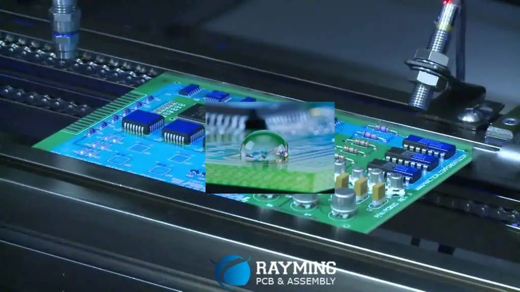
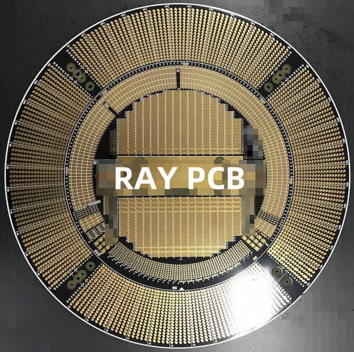
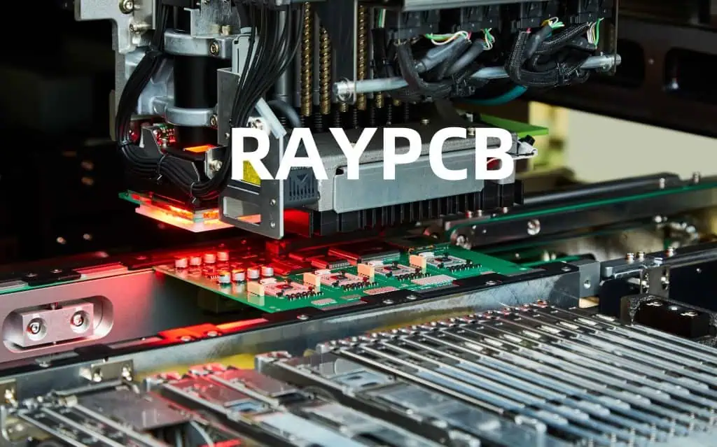
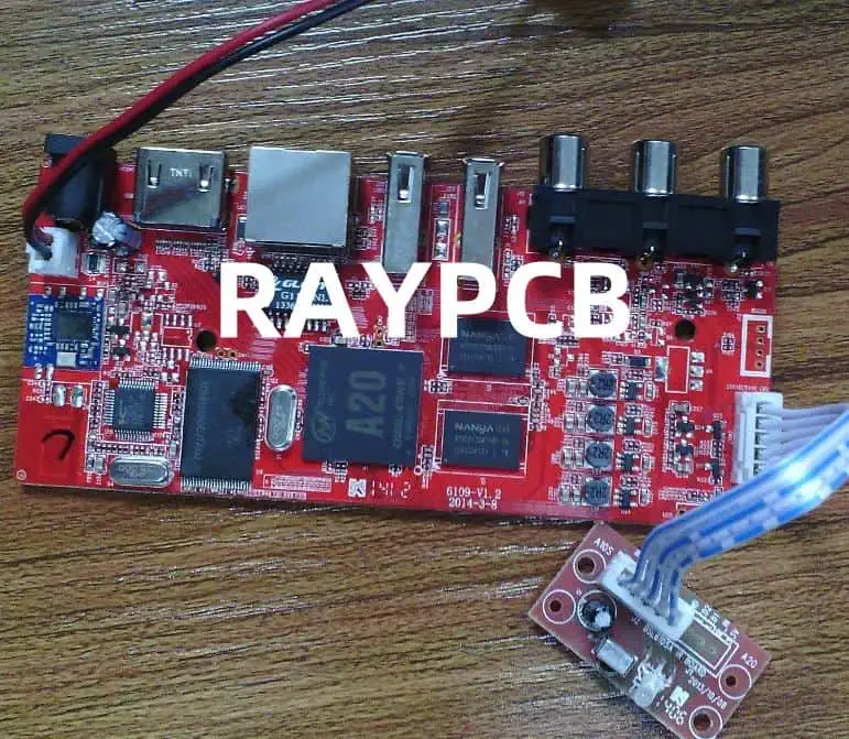
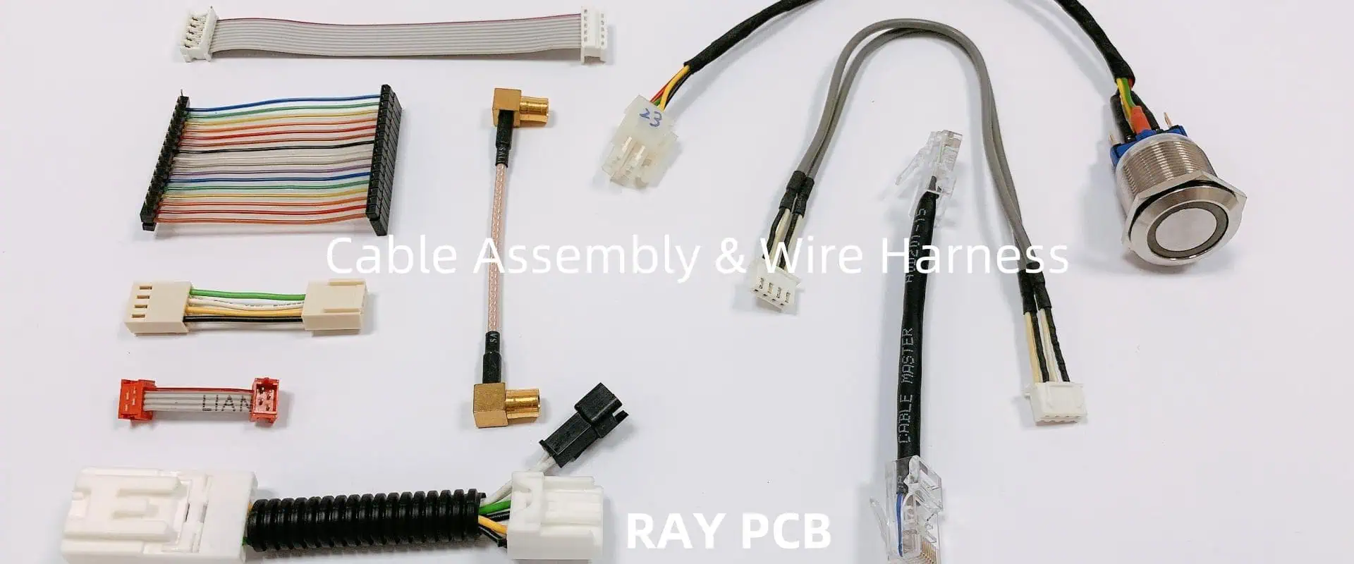
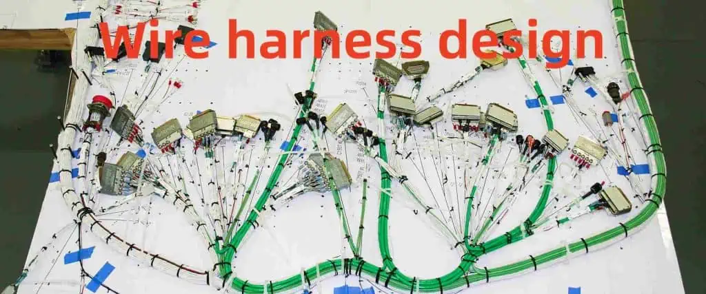
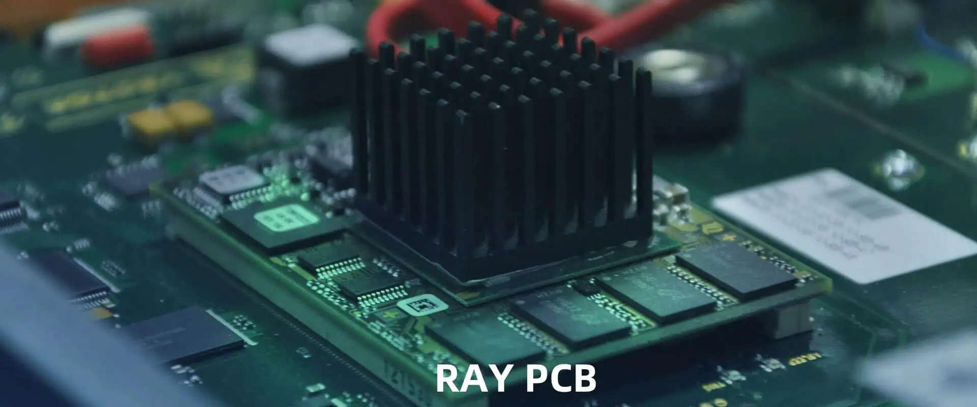
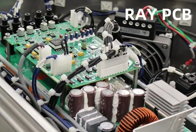
Box-build assembly is a specialized manufacturing process that involves the integration of various electronic components, mechanical parts, and software into a complete, functional unit. This process typically includes tasks such as printed circuit board (PCB) assembly, system integration, testing, and packaging.

The box-build assembly process is often utilized in the production of complex electronic devices, from industrial automation equipment to consumer electronics. The complexity of this process requires a skilled and experienced manufacturing partner who can ensure a seamless and efficient production cycle.

Factors to Consider When Choosing a Box-Build Assembly Manufacturer

When searching for the right box-build assembly manufacturer, there are several essential factors to consider. Let’s dive into each of these factors in detail:

1. Expertise and Experience

One of the most crucial factors to consider is the manufacturer’s expertise and experience in box-build assembly. Look for a company with a proven track record of successful projects, particularly in your industry or product category. Experienced manufacturers will have a deep understanding of the unique challenges and requirements associated with box-build assembly, allowing them to navigate the process efficiently and effectively.

2. Manufacturing Capabilities and Facilities

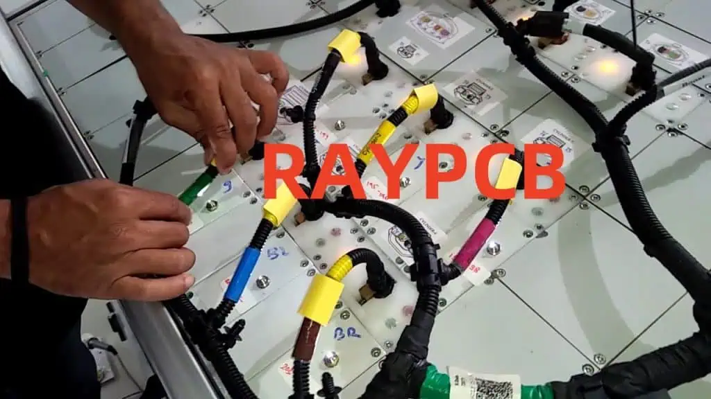
Assess the manufacturer’s manufacturing capabilities and facilities to ensure they can meet your specific needs. This includes evaluating their equipment, production capacity, quality control processes, and the overall layout and cleanliness of their production environment. A well-equipped and organized facility can greatly contribute to the overall quality and efficiency of the box-build assembly process.

3. Quality Assurance and Compliance

Quality assurance is of utmost importance in box-build assembly, as any defects or failures can have significant consequences. Look for a manufacturer with robust quality control measures, including strict testing protocols, statistical process control, and comprehensive quality management systems. Additionally, ensure that the manufacturer is compliant with industry standards and regulations relevant to your product and industry.

4. Supply Chain Management

The success of a box-build assembly project is heavily dependent on the seamless coordination and management of the supply chain. Evaluate the manufacturer’s ability to source high-quality components, manage inventory, and ensure timely deliveries. A reliable and well-organized supply chain can help mitigate delays, minimize disruptions, and maintain consistent product quality.

5. Scalability and Flexibility

As your business grows or product requirements change, the ability of the box-build assembly manufacturer to scale up or adapt to new demands is crucial. Look for a partner that can accommodate fluctuations in production volume, handle design changes, and provide scalable solutions to meet your evolving needs.

6. Collaboration and Communication

Effective collaboration and open communication are essential when working with a box-build assembly manufacturer. Assess the manufacturer’s willingness to engage with you, their responsiveness to inquiries, and their ability to provide regular updates and clear reporting. A collaborative partnership can foster innovation, problem-solving, and a smooth manufacturing process.

7. Cost-Effectiveness and Pricing

While quality and reliability should be the primary considerations, cost-effectiveness is also an important factor. Evaluate the manufacturer’s pricing structure, including setup fees, per-unit costs, and any additional charges. Seek a balance between high-quality services and competitive pricing to ensure a favorable return on your investment.

Identifying the Right Box-Build Assembly Manufacturer

To identify the right box-build assembly manufacturer for your needs, follow these steps:

  1. Define your requirements: Clearly outline your product specifications, production volumes, timeline, and any other critical requirements. This will help you narrow down the list of potential manufacturers.
  2. Conduct research and create a shortlist: Leverage industry directories, online reviews, and referrals from your network to identify reputable box-build assembly manufacturers. Create a shortlist of potential partners that meet your initial criteria.
  3. Evaluate the shortlisted manufacturers: Reach out to the shortlisted manufacturers and request detailed information about their capabilities, experience, quality assurance processes, and pricing. Arrange site visits or virtual tours to assess their facilities and operations firsthand.
  4. Compare and select: Carefully evaluate each manufacturer based on the factors discussed earlier, such as expertise, manufacturing capabilities, quality assurance, supply chain management, scalability, and collaboration. Compare the options and select the manufacturer that best aligns with your needs and offers the most compelling value proposition.
  5. Establish a collaborative partnership: Once you’ve selected the box-build assembly manufacturer, work closely with them to establish clear communication channels, define project milestones, and ensure a smooth manufacturing process. Maintain an open and transparent relationship to address any challenges that may arise.

FAQs

1. What are the key benefits of working with a experienced box-build assembly manufacturer?

The key benefits of working with an experienced box-build assembly manufacturer include:

  • Expertise in navigating the complexities of the box-build assembly process
  • Efficient and streamlined production, leading to faster time-to-market
  • Consistent high-quality outputs and reliable product performance
  • Effective supply chain management and access to quality components
  • Scalability to accommodate changes in production volume or requirements
  • Collaborative problem-solving and continuous improvement

2. How can I ensure the box-build assembly manufacturer maintains quality standards?

To ensure the box-build assembly manufacturer maintains quality standards, consider the following:

  • Thoroughly review their quality assurance processes, including testing protocols, statistical process control, and quality management systems.
  • Request regular quality reports and inspection data to monitor performance.
  • Establish clear quality metrics and key performance indicators (KPIs) to track progress.
  • Conduct on-site audits or inspections to verify the manufacturing environment and processes.
  • Implement regular quality control checkpoints throughout the production cycle.

3. What are the common challenges in box-build assembly, and how can a manufacturer help address them?

Some of the common challenges in box-build assembly include:

  • Managing complex supply chains and component sourcing
  • Ensuring seamless system integration and compatibility
  • Maintaining strict tolerances and quality control
  • Accommodating design changes and product iterations
  • Scaling production capacity to meet fluctuating demands

An experienced box-build assembly manufacturer can help address these challenges by:

  • Maintaining a robust and flexible supply chain
  • Leveraging their expertise in system integration and testing
  • Implementing robust quality control measures and continuous improvement
  • Providing flexible and scalable manufacturing solutions
  • Fostering open communication and collaboration throughout the project

4. How can I evaluate the financial stability and long-term viability of a box-build assembly manufacturer?

To assess the financial stability and long-term viability of a box-build assembly manufacturer, consider the following:

  • Review their financial statements, including revenue, profits, and asset-to-liability ratios.
  • Examine their client portfolio and track record of successful projects.
  • Inquire about their investment in technology, equipment, and infrastructure.
  • Assess their ability to adapt to market changes and evolving industry trends.
  • Evaluate their workforce stability, employee retention, and succession planning.
  • Consult industry sources and reference checks to gather insights into their overall reputation and financial health.

5. What are the key factors to consider when negotiating a contract with a box-build assembly manufacturer?

When negotiating a contract with a box-build assembly manufacturer, consider the following key factors:

  • Clearly define the scope of work, deliverables, and timeline.
  • Establish quality control measures and acceptance criteria.
  • Agree on pricing structures, including setup fees, per-unit costs, and any additional charges.
  • Outline the process for handling design changes, product modifications, and escalations.
  • Stipulate the manufacturer’s responsibilities for supply chain management and inventory control.
  • Include provisions for intellectual property protection, confidentiality, and data security.
  • Specify the terms for termination, dispute resolution, and any applicable warranties or guarantees.

By thoroughly evaluating these factors and negotiating a comprehensive contract, you can ensure a mutually beneficial partnership with the box-build assembly manufacturer.

Conclusion

Identifying the right box-build assembly manufacturer is a critical decision that can significantly impact the success of your product. By considering factors such as expertise, manufacturing capabilities, quality assurance, supply chain management, scalability, and collaboration, you can find a manufacturing partner that aligns with your specific needs and helps you achieve your business objectives. Remember to thoroughly research, evaluate, and establish a collaborative relationship with the selected manufacturer to ensure a smooth and successful box-build assembly process.

Common Mistakes to Avoid in PCB Layout Design for Manufacturability!

Printed Circuit Board (PCB) layout design is a crucial aspect of the product development process, as it directly impacts the manufacturability, performance, and reliability of the final product. Overlooking common design pitfalls can lead to a range of issues, including increased production costs, extended lead times, and even product failures. In this comprehensive guide, we will delve into the most common mistakes to avoid in PCB layout design for enhanced manufacturability.

Importance of Manufacturability in PCB Layout Design

The layout design of a PCB plays a pivotal role in determining its overall manufacturability. A well-designed layout not only ensures the proper functioning of the circuit but also facilitates the efficient and cost-effective production of the board. Conversely, poorly designed layouts can introduce a myriad of challenges during the manufacturing process, resulting in increased scrap rates, yield losses, and higher overall costs.

By understanding and avoiding common design pitfalls, PCB designers can optimize their layouts to meet the requirements of modern manufacturing processes, ultimately delivering high-quality products to their customers in a timely and cost-effective manner.

Common Mistakes to Avoid in PCB Layout Design

To ensure the manufacturability of your PCB, it is essential to be aware of the following common mistakes and how to address them effectively:

1. Insufficient Trace and Space Clearance

Trace and space clearance refer to the distance between adjacent copper traces and the spacing between pads or traces. Inadequate clearance can lead to several manufacturing issues, such as:

  • Shorts and Electrical Leakage: Insufficient clearance can result in short circuits or electrical leakage between traces, compromising the performance and reliability of the PCB.
  • Difficulty in Etching and Plating: Tight clearances can make it challenging for the manufacturing process to accurately etch and plate the copper layers, leading to defects and yield losses.
  • Challenges in Solder Mask Application: Insufficient clearance can complicate the solder mask application process, increasing the risk of solder bridges and other assembly-related issues.

To ensure proper manufacturability, it is recommended to follow the minimum trace and space clearance guidelines provided by the PCB manufacturer or industry standards, such as IPC-2221 or IPC-2222.

2. Improper Via Placement and Design

Vias are essential for connecting different copper layers in a multilayer PCB. However, improper via placement and design can introduce several manufacturing challenges, including:

  • Difficulty in Drilling and Plating: Poorly placed vias or vias with unsuitable dimensions can make the drilling and plating processes more challenging, leading to increased defects and reduced yields.
  • Reliability Concerns: Vias that are too close to the board edge or other features can compromise the overall structural integrity and reliability of the PCB.
  • Impedance Mismatches: Vias with incorrect dimensions or improper placement can cause impedance mismatches, leading to signal integrity issues and potential performance degradation.

To address these challenges, it is crucial to follow the via design guidelines provided by the PCB manufacturer, considering factors such as via diameter, aspect ratio, and placement relative to other board features.

3. Inadequate Copper Weight and Trace Width

The copper weight and trace width of a PCB play a significant role in its manufacturability, electrical performance, and thermal management. Overlooking these design considerations can result in the following issues:

  • Difficulty in Etching and Plating: Thick copper layers or wide traces can make the etching and plating processes more challenging, increasing the risk of defects and reducing overall yields.
  • Thermal Management Challenges: Insufficient copper weight or narrow trace widths can limit the PCB’s ability to dissipate heat, leading to thermal management issues and potential performance degradation.
  • Electrical Performance Concerns: Improper copper weight or trace width can result in impedance mismatches, signal integrity problems, and other electrical performance issues.

To ensure optimal manufacturability and performance, it is essential to select the appropriate copper weight and trace widths based on the specific requirements of the PCB design, considering factors such as current-carrying capacity, thermal management, and electrical performance.

4. Insufficient Solder Mask Clearance

The solder mask is a critical component of the PCB, as it serves to protect the copper traces and prevent short circuits during the assembly process. Inadequate solder mask clearance can lead to the following issues:

  • Solder Bridging and Shorts: Insufficient clearance between the solder mask and the copper traces can result in solder bridges and short circuits during the assembly process.
  • Difficulty in Solder Mask Application: Tight clearances can make it challenging for the manufacturing process to accurately apply the solder mask, leading to defects and reduced yields.
  • Increased Risk of Damage: Insufficient clearance can increase the risk of damage to the solder mask during the manufacturing and assembly processes, compromising the overall reliability of the PCB.

To mitigate these issues, it is recommended to follow the solder mask clearance guidelines provided by the PCB manufacturer or industry standards, such as IPC-2221 or IPC-7351.

5. Improper Silkscreen Placement and Design

PCB silkscreen
PCB silkscreen

The silkscreen, which includes the component designators, logos, and other surface markings, is an essential element of the PCB layout. Improper silkscreen placement and design can lead to the following challenges:

  • Interference with Assembly: Silkscreen elements that overlap with component placement areas or interfere with the assembly process can result in manufacturing issues and potential product failures.
  • Reduced Readability: Poorly designed or positioned silkscreen elements can make it difficult for the assembly technicians to identify and orient the components correctly, leading to assembly errors.
  • Cosmetic Defects: Improper silkscreen placement or design can result in aesthetic issues, such as overlapping or misaligned markings, which can be undesirable for the end-user.

To ensure optimal manufacturability and usability, it is essential to carefully plan the silkscreen layout, considering the placement of components, assembly processes, and overall readability of the markings.

6. Disregard for Manufacturing Tolerances

Thickness & Tolerances For PCB Laminates

Every manufacturing process has inherent tolerances and limitations that must be taken into account during the PCB layout design. Disregarding these tolerances can lead to a range of issues, including:

  • Yield Losses: Failing to account for manufacturing tolerances can result in the production of non-conforming boards, leading to increased scrap rates and reduced yields.
  • Reliability Concerns: Ignoring manufacturing tolerances can compromise the structural integrity and long-term reliability of the PCB, potentially leading to premature failures in the field.
  • Increased Costs: Neglecting manufacturing tolerances can necessitate the use of tighter design rules, which can significantly increase the overall cost of the PCB production.

To address this challenge, it is crucial to closely collaborate with the PCB manufacturer, understand their specific capabilities and tolerances, and design the layout accordingly. This may involve the use of design-for-manufacturing (DFM) tools or seeking guidance from the manufacturer’s technical support team.

7. Lack of Consideration for Test and Inspection Processes

The PCB layout design should also consider the requirements of the test and inspection processes during manufacturing. Overlooking these aspects can lead to the following issues:

  • Difficulty in Testing: Poorly designed test points or inaccessible components can make it challenging to effectively test the PCB during the manufacturing process, leading to reduced quality and increased rework.
  • Inspection Challenges: Obstructed or hard-to-reach areas on the PCB can make it difficult for the manufacturing team to perform visual inspections, increasing the risk of undetected defects.
  • Reliability Concerns: Failure to consider the test and inspection requirements can result in the production of PCBs with hidden defects or reliability issues that may only surface later in the product’s lifecycle.

To address these challenges, it is essential to collaborate with the manufacturing team, understand their test and inspection requirements, and incorporate design elements that facilitate efficient and effective quality assurance processes.

8. Disregard for Component Placement and Orientation

The placement and orientation of components on the PCB can significantly impact the overall manufacturability and assembly process. Ignoring these considerations can lead to the following issues:

  • Assembly Difficulties: Poorly placed or oriented components can make the assembly process more challenging, leading to increased errors, rework, and reduced efficiency.
  • Interference with Other Components: Improper component placement can result in interference with neighboring components, causing clearance issues and potential performance degradation.
  • Thermal Management Concerns: Inadequate spacing or improper placement of heat-generating components can lead to thermal management problems and potential performance issues.

To ensure optimal component placement and orientation, it is essential to consider factors such as component size, heat generation, assembly process requirements, and overall board layout optimization.

9. Lack of Design for Testability (DFT)

Design for Testability (DFT) is a crucial aspect of PCB layout design that ensures the board can be effectively tested and diagnosed during the manufacturing process. Neglecting DFT can result in the following problems:

  • Difficulty in Testing: Poorly designed test points or a lack of testability features can make it challenging to thoroughly test the PCB, leading to reduced quality and increased rework.
  • Increased Debugging Efforts: Without proper DFT considerations, identifying and resolving issues during the manufacturing process can become more time-consuming and costly.
  • Reduced Fault Coverage: Insufficient DFT features can result in lower fault coverage during testing, increasing the risk of undetected defects and potential product failures.

To address these challenges, it is essential to incorporate DFT principles into the PCB layout design, such as strategically placed test points, built-in self-test (BIST) capabilities, and other testability features that facilitate efficient and effective quality assurance.

10. Disregard for Manufacturing Processes and Equipment Capabilities

Each PCB manufacturing facility has its own set of processes, equipment, and capabilities. Failing to consider these factors during the layout design can lead to a range of issues, including:

  • Incompatibility with Manufacturing Processes: Designing a layout that is not compatible with the manufacturer’s processes can result in production challenges, increased lead times, and higher costs.
  • Limitations of Manufacturing Equipment: Ignoring the capabilities of the manufacturer’s equipment, such as drill bit sizes, plating thickness, or board size limitations, can lead to design-related defects and reduced yields.
  • Lack of Design Optimization: Disregarding the manufacturer’s specific capabilities can prevent the designer from optimizing the layout for the most cost-effective and efficient production.

To address this challenge, it is essential to engage with the PCB manufacturer early in the design process, understand their capabilities, and design the layout accordingly. This collaborative approach can help ensure the manufacturability and cost-effectiveness of the final product.

FAQ

Q1: What are the consequences of insufficient trace and space clearance in PCB layout design?

A1: Insufficient trace and space clearance can lead to several manufacturing issues, including:

  • Shorts and electrical leakage due to the proximity of traces
  • Difficulty in the etching and plating processes, resulting in defects and yield losses
  • Challenges in the solder mask application, increasing the risk of solder bridges and other assembly-related issues

To ensure proper manufacturability, it is recommended to follow the minimum trace and space clearance guidelines provided by the PCB manufacturer or industry standards.

Q2: How can improper via placement and design impact the PCB manufacturing process?

A2: Improper via placement and design can introduce several challenges, such as:

  • Difficulty in drilling and plating the vias, leading to increased defects and reduced yields
  • Reliability concerns due to vias placed too close to the board edge or other features
  • Impedance mismatches caused by vias with incorrect dimensions or placement, leading to signal integrity issues

To address these challenges, it is crucial to follow the via design guidelines provided by the PCB manufacturer and consider factors like via diameter, aspect ratio, and placement relative to other board features.

Q3: What are the consequences of inadequate copper weight and trace width in PCB layout design?

A3: Inadequate copper weight or trace width can result in the following issues:

  • Difficulty in the etching and plating processes, increasing the risk of defects and reducing overall yields
  • Thermal management challenges due to limited heat dissipation capabilities
  • Electrical performance concerns, such as impedance mismatches and signal integrity problems

To ensure optimal manufacturability and performance, it is essential to select the appropriate copper weight and trace widths based on the specific requirements of the PCB design.

Q4: How can insufficient solder mask clearance impact the PCB manufacturing process?

A4: Insufficient solder mask clearance can lead to the following issues:

  • Solder bridging and shorts during the assembly process due to the proximity of the copper traces
  • Difficulty in the solder mask application, resulting in defects and reduced yields
  • Increased risk of damage to the solder mask during manufacturing and assembly

To mitigate these issues, it is recommended to follow the solder mask clearance guidelines provided by the PCB manufacturer or industry standards.

Q5: Why is it important to consider manufacturing tolerances during the PCB layout design process?

A5: Disregarding manufacturing tolerances can lead to several problems, including:

  • Yield losses due to the production of non-conforming boards
  • Reliability concerns as the structural integrity and long-term performance of the PCB may be compromised
  • Increased overall costs, as the use of tighter design rules may be necessary to accommodate the manufacturing limitations

To address this challenge, it is crucial to collaborate with the PCB manufacturer, understand their specific capabilities and tolerances, and design the layout accordingly.

Best Practice for PCB Moisture Protection in Outdoor Environments

Printed Circuit Boards (PCBs) are the backbone of modern electronic devices, enabling the integration of complex circuitry and components. However, when these PCBs are exposed to outdoor environments, they face a unique set of challenges, particularly when it comes to protecting them from moisture-related issues. Exposure to moisture, humidity, and other environmental factors can lead to a range of problems, including corrosion, electrical failures, and reduced product lifespan.

In this comprehensive guide, we will explore the best practices for PCB moisture protection in outdoor environments, covering the various strategies and techniques that can be employed to ensure the long-term reliability and performance of your electronic devices.

Understanding the Challenges of Outdoor Environments

Waterproof pcb

Outdoor environments present a unique set of challenges for PCB protection, as they are subject to a wide range of environmental factors that can compromise the integrity of the electronic components and the PCB itself. Some of the key challenges include:

  1. Moisture and Humidity: Outdoor environments are often characterized by high humidity, rain, and even condensation, which can lead to the accumulation of moisture on the PCB surface and within the components.
  2. Temperature Fluctuations: Outdoor environments typically experience significant temperature variations, from extreme heat to frigid cold, which can cause thermal stress and expansion/contraction of the PCB and its components.
  3. Dust and Debris: Outdoor environments are prone to the accumulation of dust, dirt, and other particulate matter, which can interfere with the proper functioning of the PCB and its components.
  4. UV Exposure: Prolonged exposure to direct sunlight and ultraviolet (UV) radiation can degrade the materials used in PCB construction, leading to discoloration, embrittlement, and other forms of degradation.
  5. Corrosion: The combination of moisture, humidity, and various environmental pollutants can accelerate the corrosion of the PCB’s metal components, including the copper traces and solder joints.

To address these challenges and ensure the long-term reliability of PCBs in outdoor environments, a comprehensive approach to moisture protection is necessary.

Strategies for PCB Moisture Protection

Effective PCB moisture protection in outdoor environments involves a combination of design, material selection, and specialized manufacturing processes. Let’s explore the key strategies and best practices:

1. Waterproofing and Conformal Coating

One of the most important steps in protecting PCBs from moisture is the application of a waterproofing or conformal coating. These coatings act as a barrier, preventing the ingress of moisture, dust, and other environmental contaminants.

Waterproofing Coatings

Waterproofing coatings, such as acrylic, epoxy, or silicone-based materials, create a robust, water-resistant barrier on the PCB surface. These coatings can be applied through various methods, including dipping, spraying, or brushing. The selection of the appropriate waterproofing coating depends on factors such as the PCB’s operating environment, the required level of protection, and the compatibility with the PCB materials.

Conformal Coatings

Conformal coatings are thin, flexible, and transparent films that conform to the shape of the PCB and its components. These coatings provide protection against moisture, dust, and other environmental factors, while also offering some degree of electrical insulation. Common conformal coating materials include acrylic, polyurethane, silicone, and parylene.

The selection of the appropriate conformal coating depends on factors such as the required level of protection, the operating temperature range, and the chemical and electrical compatibility with the PCB components.

2. Potting and Encapsulation

In addition to waterproofing and conformal coatings, potting and encapsulation techniques can provide an additional layer of protection for PCBs in outdoor environments.

Potting

Potting involves filling the entire PCB assembly or specific components with a protective, polymeric material, such as epoxy or polyurethane. This creates a solid, waterproof, and impact-resistant enclosure that seals the PCB and its components from the external environment.

Potting is particularly effective in protecting against moisture, vibration, and physical damage, but it can also add weight and volume to the overall assembly.

Encapsulation

Encapsulation is a similar process to potting, but it typically involves the selective encapsulation of specific components or areas of the PCB, rather than the entire assembly. This approach can provide targeted protection while maintaining a more compact and lightweight design.

Encapsulation materials, such as epoxy or silicone-based resins, are carefully selected to ensure compatibility with the PCB components and to provide the required level of protection.

3. Thermal Management

Effective thermal management is crucial for PCBs in outdoor environments, as temperature fluctuations can lead to moisture condensation and other related issues.

Heatsinks and Thermal Interfaces

Heat Sink PCB

The use of heatsinks and thermal interface materials (TIMs) can help dissipate heat generated by the PCB components, reducing the risk of moisture condensation and improving overall reliability.

Heatsinks are designed to efficiently transfer heat from the PCB components to the surrounding environment, while TIMs, such as thermal greases or phase change materials, improve the thermal conductivity between the components and the heatsink.

Ventilation and Airflow

Ensuring adequate ventilation and airflow around the PCB can help prevent the buildup of heat and moisture. This can be achieved through the use of air vents, fans, or other passive or active cooling solutions, depending on the specific requirements of the outdoor application.

4. Humidity and Moisture Control

In addition to waterproofing and thermal management, controlling the humidity and moisture levels within the PCB enclosure or assembly is crucial for long-term reliability.

Desiccant Packs

Desiccant packs can be used to absorb and remove excess moisture from the enclosed environment, preventing the formation of condensation and reducing the risk of corrosion.

These desiccant packs are typically made of materials like silica gel or calcium oxide and can be strategically placed within the PCB enclosure to maintain a low-humidity environment.

Dehumidification Systems

For more advanced outdoor applications, the use of active dehumidification systems may be necessary. These systems actively monitor and control the humidity levels within the PCB enclosure, ensuring that the relative humidity remains within the optimal range for the PCB’s reliable operation.

5. Environmental Sealing and Gaskets

To complement the moisture protection strategies mentioned above, effective environmental sealing and the use of gaskets can further enhance the PCB’s resistance to moisture, dust, and other contaminants.

Enclosure Sealing

The PCB enclosure or housing should be designed with robust sealing mechanisms, such as O-rings, lip seals, or gaskets, to prevent the ingress of moisture, dust, and other environmental factors.

The selection of the appropriate sealing materials and the proper design of the sealing interfaces are crucial to ensuring a reliable and long-lasting seal.

Gasket Selection

Gaskets, made from materials like neoprene, silicone, or EPDM, can be used to create tight seals between the PCB enclosure and other mating surfaces, further enhancing the overall moisture protection.

The choice of gasket material and design should consider factors such as the operating temperature range, chemical compatibility, and the required level of compression and sealing performance.

Specialized Manufacturing Processes

In addition to the design and material selection strategies, specialized manufacturing processes can also contribute to improved PCB moisture protection in outdoor environments.

Conformal Coating Application

The application of conformal coatings is a critical process that requires careful attention to detail. Factors such as surface preparation, coating thickness, and curing conditions can all impact the effectiveness of the conformal coating in providing moisture protection.

Advanced techniques, such as automated spray coating or selective coating processes, can help ensure consistent and reliable conformal coating application.

Potting and Encapsulation Processes

The potting and encapsulation processes for PCBs in outdoor environments require specialized equipment and expertise to ensure proper material mixing, void-free filling, and reliable curing.

Automated dispensing systems, controlled curing environments, and quality control measures are essential to producing high-quality, moisture-resistant potted or encapsulated PCB assemblies.

Environmental Testing and Validation

To ensure the long-term reliability of PCBs in outdoor environments, comprehensive environmental testing and validation are crucial. This includes exposing the PCB assemblies to simulated environmental conditions, such as temperature and humidity cycling, salt spray, and UV exposure, to assess their performance and integrity.

The results of these tests can help validate the effectiveness of the moisture protection strategies and guide further refinements in the design and manufacturing processes.

FAQ

PCB Assembly conformal coating

Q1: What are the key considerations when selecting a waterproofing or conformal coating for PCBs in outdoor environments?

A1: The key considerations when selecting a waterproofing or conformal coating include:

  • Compatibility with the PCB materials and components
  • Ability to provide a durable, long-lasting barrier against moisture and other environmental factors
  • Resistance to temperature fluctuations, UV exposure, and chemical exposure
  • Ease of application and curing requirements
  • Potential impact on the electrical and thermal performance of the PCB

Q2: How do potting and encapsulation techniques differ in terms of PCB moisture protection?

A2: Potting involves filling the entire PCB assembly with a protective polymeric material, creating a solid, waterproof enclosure. Encapsulation, on the other hand, selectively encapsulates specific components or areas of the PCB. Potting provides more comprehensive protection but adds weight and volume, while encapsulation offers targeted protection with a more compact design.

Q3: What are the advantages of using desiccant packs and dehumidification systems for PCB moisture protection in outdoor environments?

A3: Desiccant packs and dehumidification systems help maintain low humidity levels within the PCB enclosure, preventing the formation of condensation and reducing the risk of corrosion. Desiccant packs are a passive solution, while dehumidification systems actively monitor and control the humidity levels, providing more precise and reliable moisture control.

Q4: How do environmental sealing and gasket selection contribute to PCB moisture protection in outdoor environments?

A4: Effective environmental sealing, using techniques like O-rings, lip seals, and gaskets, helps prevent the ingress of moisture, dust, and other contaminants into the PCB enclosure. The selection of the appropriate sealing materials and the proper design of the sealing interfaces are crucial to ensuring a reliable and long-lasting seal.

Q5: What is the importance of environmental testing and validation in ensuring the long-term reliability of PCBs in outdoor environments?

A5: Environmental testing and validation are essential to verifying the effectiveness of the moisture protection strategies employed. By exposing PCB assemblies to simulated environmental conditions, such as temperature and humidity cycling, salt spray, and UV exposure, manufacturers can assess the performance and integrity of the PCB over its expected lifetime. This validation process helps identify potential weaknesses and guides further refinements in the design and manufacturing processes.

A Comprehensive Guide for Multilayer PCB Fabrication Process!

Multilayer Printed Circuit Boards (PCBs) are an essential component in modern electronics, enabling the integration of complex circuitry and components within a compact and efficient package. The fabrication process for multilayer PCBs involves a series of intricate steps, each requiring meticulous attention to detail to ensure the final product’s quality and reliability. In this comprehensive guide, we will delve into the various stages of the multilayer PCB fabrication process, providing an in-depth understanding of the techniques and considerations involved.

Overview of Multilayer PCB Fabrication

Multilayer PCBs are constructed by stacking multiple layers of copper-clad dielectric materials, each layer containing a specific circuit design. These layers are then bonded together using a lamination process, creating a multi-layered structure that allows for greater component density and enhanced electrical performance.

The multilayer PCB fabrication process typically consists of the following key stages:

  1. Prepregs and Core Preparation
  2. Drilling and Plating
  3. Imaging and Etching
  4. Multilayer Lamination
  5. Final Finishing and Inspection

Let’s explore each of these stages in detail.

Prepregs and Core Preparation

PCB Core &. Prepreg Materials

The foundation of a multilayer PCB is the core and prepreg materials. The core is a rigid, double-sided copper-clad laminate that forms the inner layers of the PCB. The prepreg, on the other hand, is a semi-cured, resin-impregnated glass-fiber material that is used to bond the core layers together during the lamination process.

Core Materials

The core materials used in multilayer PCB fabrication are typically made of a dielectric substrate, such as fiberglass-reinforced epoxy (FR-4), polyimide, or ceramic, with copper foil laminated on both sides. These core materials provide the mechanical support and electrical insulation necessary for the circuit traces and components.

The selection of the core material is crucial, as it must meet specific requirements, such as:

Table 1 provides a comparison of common core materials used in multilayer PCB fabrication:

MaterialDielectric Constant (Dk)Dissipation Factor (Df)Thermal Conductivity (W/m-K)
FR-44.2 – 4.70.017 – 0.0200.3 – 0.4
Polyimide3.4 – 3.80.002 – 0.0040.4 – 0.6
Ceramic3.8 – 9.80.001 – 0.00320 – 40

Prepreg Materials

The prepreg materials used in multilayer PCB fabrication are typically made of a woven glass-fiber mat impregnated with a thermosetting resin, such as epoxy or polyimide. The prepreg acts as an adhesive layer that bonds the core layers together during the lamination process.

The selection of the prepreg material is crucial, as it must have the following properties:

  • Suitable dielectric properties to maintain signal integrity
  • Appropriate flow and melt viscosity for uniform bonding
  • Thermal stability to withstand the high temperatures during fabrication
  • Chemical resistance to withstand the various chemicals used in the process

Table 2 provides a comparison of common prepreg materials used in multilayer PCB fabrication:

MaterialDielectric Constant (Dk)Dissipation Factor (Df)Resin Flow
Epoxy Prepreg4.0 – 4.50.015 – 0.020Medium
Polyimide Prepreg3.2 – 3.60.002 – 0.004Low
Cyanate Ester Prepreg3.0 – 3.40.005 – 0.008Medium

Drilling and Plating

PCB drilling machine

After the core and prepreg materials have been prepared, the next step in the multilayer PCB fabrication process is drilling and plating.

Drilling

The drilling process involves the creation of vias, which are holes that provide electrical interconnections between the different layers of the PCB. These vias can be classified into two main types:

  1. Plated-through Holes (PTHs): These are holes that are drilled through the entire thickness of the PCB and are subsequently plated with a conductive material, typically copper, to create an electrical connection between the layers.
  2. Blind Vias: These are holes that are drilled and plated, but do not extend through the entire thickness of the PCB. They are used to connect specific layers within the multilayer structure.

The drilling process requires precise control over the hole size, location, and depth to ensure reliable interconnections and maintain the overall structural integrity of the PCB.

Plating

After the drilling process, the vias are plated with a conductive material, typically copper, to create the electrical connections between the layers. This plating process involves several steps:

  1. Desmearing: The inner walls of the drilled holes are chemically treated to remove any resin residue, ensuring a clean surface for the plating process.
  2. Catalyzation: A catalytic layer, such as palladium, is deposited on the inner walls of the holes to facilitate the subsequent electroplating process.
  3. Electroplating: Copper is electrochemically deposited on the inner walls of the holes, creating a continuous conductive path between the layers.
  4. Copper Thickness Adjustment: The copper thickness on the inner walls of the vias is adjusted to meet the design specifications, typically ranging from 15 to 35 microns.

The plating process is crucial for ensuring reliable electrical connections and maintaining the overall structural integrity of the multilayer PCB.

Imaging and Etching

Strip film etching line

After the drilling and plating processes, the next step in the multilayer PCB fabrication process is imaging and etching.

Imaging

The imaging process involves the transfer of the circuit pattern onto the copper-clad layers of the PCB. This is typically done using one of the following methods:

  1. Photolithography: A photoresist material is applied to the copper-clad layers, and the circuit pattern is transferred using a photomask and UV light exposure.
  2. Direct Imaging: The circuit pattern is directly imaged onto the photoresist-coated copper layers using a high-resolution laser or DLP (Digital Light Processing) system, eliminating the need for a photomask.

The imaging process ensures that the desired circuit pattern is accurately transferred to the copper layers, providing the foundation for the subsequent etching process.

Etching

The etching process involves the selective removal of unwanted copper from the PCB layers, leaving behind the desired circuit patterns. This is typically done using a chemical etching process, where the exposed copper is dissolved by a chemical etchant, such as ferric chloride or ammoniacal copper etchant.

The etching process requires precise control over the etchant concentration, temperature, and exposure time to ensure the accurate reproduction of the circuit patterns and maintain the desired copper thickness.

After the etching process, the remaining photoresist is removed, leaving behind the desired circuit patterns on the PCB layers.

Multilayer Lamination

PCB Multilayer Pressing equipment

The next step in the multilayer PCB fabrication process is the lamination of the individual layers to form the final multilayer structure.

Lay-up

The lay-up process involves the stacking and alignment of the individual PCB layers, including the core, prepreg, and any additional layers, such as copper foils or solder masks. The layers are carefully aligned to ensure accurate positioning of the circuit patterns and vias.

Lamination

The lamination process involves the application of heat and pressure to bond the individual layers together, creating the multilayer PCB structure. During this process, the prepreg material melts and flows, filling any gaps between the layers and creating a strong, uniform bond.

The lamination process is typically performed in a hydraulic press or a vacuum lamination machine, with precise control over the temperature, pressure, and duration to ensure the optimal bonding of the layers.

Dimensional Stability

After the lamination process, the multilayer PCB undergoes a cooling phase to solidify the bond between the layers. During this cooling process, it is essential to maintain the dimensional stability of the PCB to ensure the accurate alignment of the circuit patterns and vias.

The dimensional stability of the multilayer PCB is influenced by factors such as the material properties of the core and prepreg, the lamination conditions, and the thermal management during the fabrication process.

Final Finishing and Inspection

9 PCB inspection precautions

The final stage of the multilayer PCB fabrication process involves the finishing steps and the inspection of the final product.

Final Finishing

The finishing steps include the following:

  1. Outer Layer Imaging and Etching: The outer layers of the multilayer PCB are imaged and etched to create the final circuit patterns.
  2. Surface Finishing: The exposed copper surfaces are treated with a protective coating, such as gold, silver, or tin-lead, to improve solderability and corrosion resistance.
  3. Solder Mask Application: A solder mask, a protective coating that prevents solder from bridging between circuit traces, is applied to the PCB.
  4. Silkscreen Printing: Alphanumeric markings and other surface legends are printed on the PCB using a silkscreen process.

Inspection and Testing

The final multilayer PCB is thoroughly inspected and tested to ensure its quality and reliability. This includes:

  1. Visual Inspection: The PCB is visually inspected for any defects, such as scratches, misalignment, or surface blemishes.
  2. Electrical Testing: The PCB is tested for continuity, isolation, and other electrical parameters to ensure the integrity of the circuit connections.
  3. Mechanical Testing: The PCB is tested for physical properties, such as flex, twist, and thermal cycling, to ensure its structural integrity.
  4. Environmental Testing: The PCB may undergo additional environmental tests, such as temperature and humidity cycling, to assess its performance under various operating conditions.

Only after passing these rigorous inspection and testing procedures can the multilayer PCB be deemed ready for final assembly and integration into the end product.

FAQ

100-layer-PCB-circuit-board

Q1: What are the key factors to consider when selecting core and prepreg materials for multilayer PCB fabrication?

A1: The key factors to consider when selecting core and prepreg materials include:

  • Dielectric constant (Dk) and dissipation factor (Df) to maintain signal integrity
  • Thermal conductivity for heat dissipation
  • Dimensional stability for reliable interconnections
  • Chemical resistance to withstand the fabrication processes
  • Resin flow and melt viscosity for uniform bonding during lamination

Q2: What is the purpose of the desmearing process in the plating stage of multilayer PCB fabrication?

A2: The desmearing process is used to remove any resin residue from the inner walls of the drilled holes. This ensures a clean surface for the subsequent catalyzation and electroplating steps, which are crucial for creating reliable electrical connections between the layers of the multilayer PCB.

Q3: How does the choice of imaging method (photolithography vs. direct imaging) affect the multilayer PCB fabrication process?

A3: The choice of imaging method can have the following impact on the multilayer PCB fabrication process:

  • Photolithography requires the use of a photomask, which adds an additional step and can affect the overall cost and turnaround time.
  • Direct imaging eliminates the need for a photomask, simplifying the process and potentially reducing the cost and turnaround time.
  • Direct imaging can also offer higher resolution and better registration accuracy, leading to improved circuit pattern transfer.

Q4: What are the key considerations during the lamination process to ensure the dimensional stability of the final multilayer PCB?

A4: The key considerations during the lamination process to ensure dimensional stability include:

  • Precise control over temperature, pressure, and duration to optimize the bonding of the layers
  • Careful selection of core and prepreg materials with compatible thermal expansion coefficients
  • Effective thermal management during the cooling phase to minimize warping or shrinkage of the PCB

Q5: What are the common surface finishing options for multilayer PCBs, and how do they affect the PCB’s performance and reliability?

A5: The common surface finishing options for multilayer PCBs include:

  • Gold: Provides excellent solderability and corrosion resistance, but is more expensive.
  • Silver: Offers good solderability and conductivity, but is susceptible to oxidation.
  • Tin-lead: A traditional option that provides good solderability and moderate corrosion resistance. The choice of surface finishing depends on the specific application requirements, such as soldering method, operating environment, and cost considerations.

8 Effective Ways to Reduce PCB Prototype Spins

In the fast-paced world of electronics, the development and production of Printed Circuit Boards (PCBs) play a crucial role in bringing innovative products to market. However, the process of creating functional prototypes can often involve multiple iterations, or “spins,” which can significantly impact the project timeline and budget. Reducing the number of PCB prototype spins is a key challenge that engineers and designers must address to streamline the development process and deliver high-quality products more efficiently.

In this article, we’ll explore eight effective ways to reduce PCB prototype assembly spins and optimize the prototyping phase of your project.

1. Comprehensive Design Review

Importance of Design Review

Thorough design review is the foundation for reducing PCB prototype spins. By carefully examining the circuit design, component placement, and layout before the initial prototype is fabricated, you can identify and address potential issues early on, minimizing the need for subsequent prototype iterations.

Key Steps in Design Review:

  1. Schematic Validation:ย Thoroughly review the schematic design to ensure that the circuit topology, component values, and interconnections are correct.
  2. Component Selection:ย Verify that the selected components are appropriate for the intended application, meet the performance requirements, and are readily available.
  3. Layout Optimization:ย Scrutinize the PCB layout, considering factors such as signal integrity, power distribution, and thermal management to identify potential problems.
  4. Design Rule Checks:ย Perform comprehensive design rule checks to ensure that the layout adheres to the manufacturer’s guidelines and requirements.
  5. Design for Manufacturability:ย Evaluate the design for its manufacturability, taking into account factors like copper weight, solder mask, and silkscreen requirements.

By conducting a thorough design review, you can uncover and resolve issues before the prototype is fabricated, reducing the number of costly and time-consuming prototype spins.

2. Design Simulation and Verification

The Importance of Design Simulation

Design simulation and verification are crucial steps in the PCB prototype development process. By simulating the circuit behavior and verifying the design’s performance, you can identify and address potential issues early on, reducing the need for multiple prototype spins.

Key Aspects of Design Simulation and Verification:

  1. Circuit Simulation:ย Use circuit simulation software to model the behavior of the electronic circuit, including signal integrity, power distribution, and electromagnetic interference (EMI) analysis.
  2. Layout Simulation:ย Perform layout simulations to validate the performance of the PCB design, considering factors such as interconnect parasitics, crosstalk, and thermal effects.
  3. Thermal Analysis:ย Conduct thermal simulations to ensure that the PCB design can effectively manage the heat generated by the components, preventing potential overheating and reliability issues.
  4. Signal Integrity Analysis:ย Analyze the signal integrity of high-speed signals, identifying and addressing potential issues like reflections, ringing, and signal distortion.
  5. Power Integrity Analysis:ย Evaluate the power distribution network to ensure that the design provides clean and stable power to the various components on the PCB.

By thoroughly simulating and verifying the PCB design, you can identify and resolve potential issues before the prototype is fabricated, reducing the need for subsequent prototype spins.

3. Comprehensive Component Selection

The Impact of Component Selection

The selection of appropriate components for a PCB design can significantly impact the number of prototype spins required. Carefully choosing the right components that meet the design requirements and are readily available can help minimize the need for design changes and subsequent prototype iterations.

Key Considerations in Component Selection:

  1. Performance Requirements:ย Ensure that the selected components meet the electrical, mechanical, and environmental requirements of the design.
  2. Availability and Lead Times:ย Prioritize components that are readily available and have reasonable lead times to minimize delays in the prototyping and production phases.
  3. Compatibility and Interoperability:ย Verify that the selected components are compatible with each other and can be seamlessly integrated into the overall PCB design.
  4. Alternative Components:ย Identify and evaluate alternative component options that can provide similar functionality and performance, allowing for flexibility in the design process.
  5. Component Footprint and Placement:ย Consider the physical size, package type, and placement requirements of the components to ensure optimal PCB layout and minimize potential issues.

By carefully selecting the right components and evaluating their suitability for the design, you can reduce the likelihood of design changes and the need for multiple prototype spins.

4. Robust Design for Manufacturability (DFM) Practices

Importance of Design for Manufacturability

Incorporating Design for Manufacturability (DFM) practices into the PCB design process is crucial for reducing prototype spins. By ensuring that the design is optimized for the manufacturing process, you can minimize the risk of fabrication issues and the need for rework or redesign.

Key DFM Practices:

  1. Adherence to Design Rules:ย Closely follow the design rules and guidelines provided by the PCB manufacturer to ensure that the layout and component placement are compatible with their manufacturing capabilities.
  2. Copper Weight and Thickness:ย Carefully select the appropriate copper weight and thickness to meet the design’s electrical and thermal requirements while ensuring that the PCB can be reliably manufactured.
  3. Solder Mask and Silkscreen:ย Optimize the solder mask and silkscreen designs to enhance the PCB’s manufacturability and improve the overall quality of the final product.
  4. Pad and Trace Dimensions:ย Ensure that the pad and trace dimensions are within the manufacturer’s recommended ranges to facilitate reliable solder joints and minimize the risk of defects.
  5. Via and Hole Sizes:ย Choose appropriate via and hole sizes that can be reliably manufactured, avoiding potential issues like plating defects or drilling problems.

By implementing robust DFM practices throughout the design process, you can minimize the likelihood of manufacturing-related issues and reduce the need for prototype spins.

5. Effective Communication with the PCB Manufacturer

The Importance of Manufacturer Collaboration

Establishing effective communication and collaboration with the PCB manufacturer is a crucial step in reducing prototype spins. By working closely with the manufacturer, you can ensure that the design is optimized for their specific capabilities and address any potential issues before the prototyping phase.

Key Elements of Manufacturer Collaboration:

  1. Design Review with the Manufacturer:ย Engage the PCB manufacturer in the design review process, leveraging their expertise to identify potential manufacturability issues and provide guidance on design optimization.
  2. Manufacturer Design Rules and Guidelines:ย Thoroughly understand and adhere to the manufacturer’s design rules and guidelines, ensuring that the PCB design is compatible with their capabilities.
  3. Process Capabilities and Limitations:ย Discuss the manufacturer’s process capabilities and limitations, such as minimum feature sizes, layer count, and material options, to ensure that the design is optimized for their specific processes.
  4. Prototype Feedback and Iterations:ย Maintain open communication with the manufacturer during the prototype development phase, actively addressing any issues or concerns that arise and collaborating on design refinements.
  5. Ongoing Collaboration:ย Foster a collaborative relationship with the manufacturer, regularly sharing feedback, lessons learned, and best practices to continuously improve the PCB design and prototyping process.

By actively collaborating with the PCB manufacturer, you can identify and resolve potential issues early on, reducing the need for multiple prototype spins and ensuring a more efficient development process.

6. Comprehensive Testing and Validation

Importance of Testing and Validation

Thorough testing and validation of the PCB prototype are essential for identifying and addressing issues before proceeding to the next iteration. By implementing a comprehensive testing strategy, you can uncover and resolve problems early in the development process, minimizing the need for subsequent prototype spins.

Key Elements of Testing and Validation:

  1. Electrical Testing:ย Perform a range of electrical tests, such as continuity, short-circuit, and open-circuit checks, to ensure the proper functionality of the PCB’s circuits and connections.
  2. Functional Testing:ย Evaluate the PCB’s overall functionality, verifying that it meets the design specifications and performs as intended in the target application.
  3. Environmental Testing:ย Subject the prototype to simulated environmental conditions, such as temperature, humidity, and vibration, to assess its reliability and durability.
  4. EMI/EMC Testing:ย Conduct electromagnetic interference (EMI) and electromagnetic compatibility (EMC) tests to identify and address any potential issues related to signal integrity and electromagnetic compatibility.
  5. Design for Test (DFT) Strategies:ย Incorporate design for test (DFT) strategies into the PCB design, such as test points and access mechanisms, to facilitate comprehensive testing and troubleshooting.

By implementing a robust testing and validation process, you can identify and resolve issues early in the prototyping phase, reducing the need for subsequent prototype spins and ensuring a more efficient development cycle.

7. Effective Change Management

The Importance of Change Management

Effective change management is crucial in the PCB prototype development process, as design changes can significantly impact the number of prototype spins required. By establishing a structured change management process, you can ensure that design modifications are carefully evaluated, implemented, and communicated to all stakeholders, minimizing the risk of unintended consequences.

Key Elements of Change Management:

  1. Change Request and Approval Process:ย Implement a formal change request and approval process to ensure that all design modifications are thoroughly reviewed and approved before implementation.
  2. Impact Analysis:ย Conduct a comprehensive impact analysis to evaluate the potential consequences of a proposed design change, considering factors such as circuit performance, component compatibility, and manufacturing feasibility.
  3. Configuration Management:ย Maintain a robust configuration management system to track and document all design changes, enabling effective version control and traceability.
  4. Communication and Collaboration:ย Establish clear communication channels and foster collaboration between the design team, the PCB manufacturer, and other stakeholders to ensure that all parties are aware of and aligned on the proposed design changes.
  5. Documentation and Record-Keeping:ย Maintain detailed documentation and records of all design changes, including the rationale, implementation, and testing results, to facilitate future reference and troubleshooting.

By implementing an effective change management process, you can minimize the risk of unintended consequences and ensure that design modifications are implemented in a controlled and efficient manner, reducing the need for multiple prototype spins.

8. Continuous Improvement and Iteration

The Importance of Continuous Improvement

Embracing a culture of continuous improvement is essential for reducing PCB prototype spins over the long term. By constantly evaluating the prototyping process, identifying areas for improvement, and implementing corrective actions, you can continually optimize the development cycle and minimize the need for future prototype iterations.

Key Elements of Continuous Improvement:

  1. Lessons Learned and Root Cause Analysis:ย Conduct thorough reviews of the prototyping process, document lessons learned, and perform root cause analysis to identify the underlying issues that led to prototype spins.
  2. Process Optimization:ย Implement process improvements based on the lessons learned, such as refining design review checklists, improving simulation tools and techniques, or enhancing communication with the PCB manufacturer.
  3. Metrics and KPIs:ย Establish relevant metrics and key performance indicators (KPIs) to track the effectiveness of the prototyping process, such as the number of prototype spins, time-to-market, and development costs.
  4. Continuous Feedback and Collaboration:ย Maintain open communication channels with the design team, the PCB manufacturer, and other stakeholders to gather feedback, share best practices, and collaboratively identify opportunities for improvement.
  5. Training and Knowledge Sharing:ย Invest in ongoing training and knowledge-sharing initiatives to ensure that the design team stays up-to-date with the latest tools, techniques, and industry best practices for PCB prototype development.

By embracing a culture of continuous improvement, you can systematically identify and address the root causes of prototype spins, constantly refine the development process, and achieve a more efficient and cost-effective PCB prototyping experience over time.

FAQ

PCB PROTOTYPES
PCB PROTOTYPES

Q1: What is the primary benefit of conducting a comprehensive design review for PCB prototypes?

The primary benefit of conducting a comprehensive design review for PCB prototypes is to identify and address potential issues early in the development process, minimizing the need for subsequent prototype iterations. By thoroughly reviewing the schematic, component selection, PCB layout, and design for manufacturability, the design team can uncover and resolve problems before the initial prototype is fabricated, thereby reducing the number of costly and time-consuming prototype spins.

Q2: How does design simulation and verification help reduce PCB prototype spins?

Design simulation and verification help reduce PCB prototype spins by enabling the design team to identify and address potential issues before the prototype is fabricated. By simulating the circuit behavior, analyzing signal integrity, and performing thermal analysis, the team can validate the design’s performance and make necessary adjustments without the need for multiple physical prototype iterations.

Q3: What are the key considerations in selecting components for a PCB design to minimize prototype spins?

The key considerations in selecting components for a PCB design to minimize prototype spins include:

  1. Meeting the performance requirements of the design
  2. Ensuring component availability and reasonable lead times
  3. Verifying component compatibility and interoperability
  4. Identifying and evaluating alternative component options
  5. Considering the physical size, package type, and placement requirements of the components

By carefully selecting the right components that meet the design requirements and are readily available, the design team can reduce the likelihood of design changes and the need for subsequent prototype spins.

Q4: How can effective communication and collaboration with the PCB manufacturer help reduce prototype spins?

Effective communication and collaboration with the PCB manufacturer can help reduce prototype spins in several ways:

  1. Engaging the manufacturer in the design review process to identify potential manufacturability issues early on
  2. Thoroughly understanding and adhering to the manufacturer’s design rules and guidelines
  3. Discussing the manufacturer’s process capabilities and limitations to optimize the design
  4. Maintaining open communication during the prototype development phase to address any issues that arise
  5. Fostering an ongoing collaborative relationship to continuously improve the PCB design and prototyping process

By working closely with the PCB manufacturer, the design team can ensure that the design is optimized for the manufacturer’s capabilities, reducing the risk of fabrication-related issues and the need for multiple prototype spins.

Q5: What are the key elements of a continuous improvement approach to reducing PCB prototype spins?

The key elements of a continuous improvement approach to reducing PCB prototype spins include:

  1. Conducting thorough reviews of the prototyping process to document lessons learned and perform root cause analysis
  2. Implementing process improvements based on the lessons learned, such as refining design review checklists or enhancing communication with the manufacturer
  3. Establishing relevant metrics and KPIs to track the effectiveness of the prototyping process
  4. Maintaining open communication channels and collaborative relationships with the design team, PCB manufacturer, and other stakeholders
  5. Investing in ongoing training and knowledge-sharing initiatives to keep the design team up-to-date with the latest tools, techniques, and best practices

By embracing a culture of continuous improvement, the design team can systematically identify and address the root causes of prototype spins, constantly refining the development process to achieve more efficient and cost-effective PCB prototyping over time.

ATE PCB Assembly โ€“ The Trusted Interface Between PCB Manufacturer and OEM

In the dynamic landscape of electronic device manufacturing, the partnership between Original Equipment Manufacturers (OEMs) and Printed Circuit Board (PCB) manufacturers has become increasingly essential. At the heart of this collaboration lies the critical role of Automated Test Equipment (ATE) in ensuring the quality and reliability of PCB assemblies. This article will explore the significance of ATE PCB assembly, its benefits, and the best practices that enable seamless integration between PCB manufacturers and OEMs.

The Importance of ATE in PCB Assembly

Automated Test Equipment (ATE) plays a pivotal role in the PCB assembly process, serving as a trusted interface between PCB manufacturers and OEMs. By implementing comprehensive testing protocols, ATE ensures that the assembled PCBs meet the stringent quality standards set by OEMs, thereby minimizing the risk of defects and ensuring the long-term performance and reliability of the final products.

Ensuring Quality and Reliability

One of the primary functions of ATE in PCB assembly is to rigorously test the assembled boards to identify and address any defects or issues before they reach the OEM. This comprehensive testing process encompasses a wide range of checks, including:

  1. Electrical Testing:ย ATE systems can perform various electrical tests, such as continuity, short-circuit, and open-circuit checks, to ensure the proper functioning of the PCB’s circuits and connections.
  2. Component Verification:ย ATE can verify the presence, orientation, and correct placement of all components on the PCB, reducing the risk of assembly errors.
  3. Performance Validation:ย ATE can assess the PCB’s overall performance, including signal integrity, power distribution, and compliance with specifications, to ensure the board’s optimal functionality.
  4. Environmental Stress Testing:ย ATE can subject the PCB to simulated environmental conditions, such as temperature, humidity, and vibration, to evaluate its resilience and durability.

By identifying and addressing these issues early in the assembly process, ATE helps PCB manufacturers deliver consistently high-quality products to their OEM partners, ultimately enhancing the reliability and longevity of the final electronic devices.

Streamlining the Supply Chain

The integration of ATE into the PCB assembly process also plays a crucial role in streamlining the supply chain between PCB manufacturers and OEMs. By providing a standardized testing protocol and comprehensive data reporting, ATE serves as a bridge between the two entities, facilitating seamless communication and collaboration.

Key Benefits of ATE PCB Assembly:

  1. Reduced Time-to-Market:ย By identifying and resolving issues early in the assembly process, ATE helps PCB manufacturers deliver high-quality products to OEMs more efficiently, reducing the time-to-market for the final electronic devices.
  2. Improved Communication and Transparency:ย The comprehensive data generated by ATE systems enables clear communication and transparency between PCB manufacturers and OEMs, fostering a collaborative environment and building trust.
  3. Consistent Quality Assurance:ย The standardized testing protocols and data-driven approach of ATE ensure that PCB quality and reliability are consistently maintained, meeting the stringent requirements of OEMs.
  4. Enhanced Traceability:ย ATE systems provide detailed documentation and records of the testing process, enabling efficient traceability and root cause analysis in the event of any issues.
  5. Cost Optimization:ย By identifying and addressing defects early in the assembly process, ATE helps PCB manufacturers reduce the costs associated with rework, returns, and warranty claims, ultimately benefiting both the PCB manufacturer and the OEM.

Implementing Effective ATE Strategies

To fully harness the benefits of ATE in PCB assembly, PCB manufacturers and OEMs must work together to implement effective strategies and best practices. These strategies encompass various aspects, from equipment selection to data analysis and continuous improvement.

Selecting Appropriate ATE Solutions

The selection of the right ATE solution is crucial to ensuring the success of PCB assembly projects. PCB manufacturers should consider factors such as:

  1. Test Coverage:ย Evaluate the ATE system’s ability to perform comprehensive tests that address the specific requirements of the PCB design and the OEM’s quality standards.
  2. Flexibility and Scalability:ย Choose ATE systems that can adapt to changing requirements, accommodate various PCB sizes and complexities, and scale to meet the growing demands of the business.
  3. Integration Capabilities:ย Prioritize ATE solutions that seamlessly integrate with the PCB manufacturer’s existing production infrastructure, allowing for efficient data sharing and process optimization.
  4. Reliability and Maintenance:ย Ensure that the selected ATE system is reliable, well-maintained, and supported by the manufacturer, minimizing downtime and maximizing productivity.

Developing Robust Testing Protocols

Establishing comprehensive and well-designed testing protocols is essential for effective ATE implementation. PCB manufacturers should collaborate with OEMs to:

  1. Define Test Requirements:ย Clearly define the testing requirements, including electrical, functional, and environmental parameters, to ensure that the ATE system is configured to meet the OEM’s specifications.
  2. Optimize Test Sequences:ย Streamline the test sequences to minimize testing time while maintaining the required level of thoroughness, leveraging techniques like parallel testing and test optimization.
  3. Implement Statistical Process Control:ย Utilize statistical process control (SPC) methods to monitor the testing process, identify trends, and proactively address any issues that may arise.
  4. Establish Data Management Strategies:ย Develop robust data management strategies to capture, analyze, and share the test data effectively, enabling data-driven decision-making and continuous improvement.

Fostering Collaboration and Communication

Effective collaboration and communication between PCB manufacturers and OEMs are essential for the successful implementation of ATE in the PCB assembly process. Key aspects of this collaboration include:

  1. Alignment on Quality Standards:ย Ensure that both parties have a clear understanding of the quality standards, testing protocols, and acceptance criteria for the PCB assemblies.
  2. Continuous Feedback and Improvement:ย Establish open communication channels to facilitate the exchange of feedback, lessons learned, and best practices, enabling continuous improvement in the ATE process.
  3. Joint Training and Knowledge Sharing:ย Organize joint training sessions and knowledge-sharing initiatives to ensure that both the PCB manufacturer’s and OEM’s teams are well-versed in the ATE system’s capabilities and the testing protocols.
  4. Shared Data and Analytics:ย Promote the seamless sharing of test data and analytics between the PCB manufacturer and the OEM, enabling data-driven decision-making and collaborative problem-solving.

The Future of ATE in PCB Assembly

As the electronic manufacturing industry continues to evolve, the role of ATE in PCB assembly is expected to become increasingly critical. Advancements in technology, the growing complexity of PCB designs, and the heightened focus on quality and reliability will drive the continued development and adoption of ATE solutions.

Emerging Trends in ATE

Some of the key trends shaping the future of ATE in PCB assembly include:

  1. Increased Automation and Artificial Intelligence:ย ATE systems are expected to incorporate more advanced automation features and leverage artificial intelligence (AI) and machine learning (ML) algorithms to enhance test accuracy, streamline test sequences, and enable predictive maintenance.
  2. Integrated Data Analytics:ย ATE systems will become more integrated with enterprise-wide data analytics platforms, enabling PCB manufacturers and OEMs to leverage data-driven insights for continuous improvement and proactive decision-making.
  3. Connectivity and Remote Monitoring:ย ATE systems will increasingly feature enhanced connectivity and remote monitoring capabilities, allowing for real-time data access, remote diagnostics, and collaborative troubleshooting between PCB manufacturers and OEMs.
  4. Adaptability to Emerging Technologies:ย ATE solutions will need to evolve to accommodate the changing landscape of electronic manufacturing, including the integration of emerging technologies such as 5G, IoT, and advanced materials.

FAQ

Q1: What is the primary role of Automated Test Equipment (ATE) in the PCB assembly process?

The primary role of ATE in the PCB assembly process is to ensure the quality and reliability of the assembled PCBs. ATE systems perform a comprehensive set of electrical, functional, and environmental tests to identify and address any defects or issues before the PCBs are delivered to the OEM.

Q2: How does ATE help streamline the supply chain between PCB manufacturers and OEMs?

ATE helps streamline the supply chain between PCB manufacturers and OEMs in several ways:

  1. It provides a standardized testing protocol and comprehensive data reporting, enabling clear communication and transparency between the two parties.
  2. It helps identify and resolve issues early in the assembly process, reducing the time-to-market for the final electronic devices.
  3. It ensures consistent quality assurance, meeting the stringent requirements of OEMs and building trust in the partnership.
  4. It enhances traceability through detailed documentation and records of the testing process.
  5. It helps optimize costs by identifying and addressing defects early, reducing the need for rework, returns, and warranty claims.

Q3: What are the key considerations in selecting the appropriate ATE solution for PCB assembly?

When selecting an ATE solution for PCB assembly, the key considerations include:

  1. Test coverage: Evaluating the ATE system’s ability to perform comprehensive tests that address the specific requirements of the PCB design and the OEM’s quality standards.
  2. Flexibility and scalability: Choosing ATE systems that can adapt to changing requirements, accommodate various PCB sizes and complexities, and scale to meet the growing demands of the business.
  3. Integration capabilities: Prioritizing ATE solutions that seamlessly integrate with the PCB manufacturer’s existing production infrastructure, allowing for efficient data sharing and process optimization.
  4. Reliability and maintenance: Ensuring that the selected ATE system is reliable, well-maintained, and supported by the manufacturer, minimizing downtime and maximizing productivity.

Q4: How can PCB manufacturers and OEMs collaborate to develop robust testing protocols for ATE?

To develop robust testing protocols for ATE, PCB manufacturers and OEMs should collaborate on the following:

  1. Defining test requirements: Clearly defining the testing requirements, including electrical, functional, and environmental parameters, to ensure that the ATE system is configured to meet the OEM’s specifications.
  2. Optimizing test sequences: Streamlining the test sequences to minimize testing time while maintaining the required level of thoroughness, leveraging techniques like parallel testing and test optimization.
  3. Implementing statistical process control: Utilizing statistical process control (SPC) methods to monitor the testing process, identify trends, and proactively address any issues that may arise.
  4. Establishing data management strategies: Developing robust data management strategies to capture, analyze, and share the test data effectively, enabling data-driven decision-making and continuous improvement.

Q5: What are the emerging trends that will shape the future of ATE in PCB assembly?

The key emerging trends that will shape the future of ATE in PCB assembly include:

  1. Increased automation and artificial intelligence: ATE systems incorporating more advanced automation features and leveraging AI and ML algorithms to enhance test accuracy, streamline test sequences, and enable predictive maintenance.
  2. Integrated data analytics: ATE systems becoming more integrated with enterprise-wide data analytics platforms, enabling PCB manufacturers and OEMs to leverage data-driven insights for continuous improvement and proactive decision-making.
  3. Connectivity and remote monitoring: ATE systems featuring enhanced connectivity and remote monitoring capabilities, allowing for real-time data access, remote diagnostics, and collaborative troubleshooting between PCB manufacturers and OEMs.
  4. Adaptability to emerging technologies: ATE solutions evolving to accommodate the changing landscape of electronic manufacturing, including the integration of emerging technologies such as 5G, IoT, and advanced materials.

6 Common PCB Assembly Mistakes and Their Corrective Actions

PCB Assembly Introduction

Printed Circuit Boards (PCBs) are the backbone of modern electronic devices, enabling the integration of various components into a compact and efficient system. However, the assembly process of PCBs can be a complex and delicate task, and even the slightest mistake can lead to costly consequences. In this article, we will explore six common PCB assembly mistakes and their corrective actions to help you avoid these pitfalls and ensure a successful PCB assembly process.

1. Improper Component Placement

Mistake: Incorrect component placement on the PCB

Proper component placement is crucial for the functionality and reliability of a PCB. Misaligned or improperly placed components can lead to short circuits, signal interference, and even damage to the components themselves.

Corrective Actions:

  1. Carefully review the design documentation:ย Ensure that you have a clear understanding of the component placement and orientation specified in the design documentation.
  2. Double-check component orientation:ย Verify that each component is placed in the correct orientation, as indicated by the component’s pin or polarity markings.
  3. Utilize PCB design software:ย Use PCB design software to create a visual representation of the board layout and component placement. This can help you identify and correct any placement issues before the actual assembly.
  4. Implement thorough inspection procedures:ย Establish a quality control process that includes visual inspection of the assembled PCB to catch any component placement errors.

2. Solder Bridging

Mistake: Solder bridges between adjacent PCB pads or traces

Solder bridging occurs when excessive solder or solder balls form a conductive path between adjacent PCB pads or traces, leading to short circuits and potential device failures.

Corrective Actions:

  1. Optimize the solder deposition process:ย Carefully control the amount of solder applied to the PCB pads to prevent excess solder from forming bridges.
  2. Utilize proper solder paste stencil design:ย Ensure that the solder paste stencil has the appropriate aperture size and spacing to prevent solder bridging.
  3. Implement visual inspection and repair:ย Regularly inspect the assembled PCB for solder bridges and address any issues found using a solder sucker or solder wick.
  4. Consider using no-clean solder paste:ย No-clean solder paste can help reduce the risk of solder bridging by leaving behind a more robust and less conductive residue.

3. Component Misalignment

Mistake: Misaligned components on the PCB surface

Component misalignment can occur due to various reasons, such as improper component placement, inaccurate pick-and-place equipment, or unstable PCB clamping during the assembly process. Misaligned components can lead to poor electrical connections, signal integrity issues, and even mechanical stress on the components.

Corrective Actions:

  1. Verify component placement accuracy:ย Ensure that the component placement coordinates in the design documentation match the actual placement on the PCB.
  2. Optimize pick-and-place equipment settings:ย Calibrate and fine-tune the pick-and-place machine settings to improve the accuracy and consistency of component placement.
  3. Implement PCB clamping and support systems:ย Use appropriate PCB clamping and support systems to maintain the PCB’s stability during the assembly process and prevent component misalignment.
  4. Conduct regular equipment maintenance:ย Regularly maintain and calibrate the pick-and-place equipment to ensure its optimal performance and accuracy.

4. Inadequate Solder Joint Quality

Mistake: Poor solder joint quality leading to electrical and mechanical failures

Poorly formed solder joints can result in unreliable connections, increased electrical resistance, and even mechanical failures, compromising the overall performance and reliability of the PCB.

Corrective Actions:

  1. Optimize the reflow soldering process:ย Ensure that the reflow soldering profile (temperature, time, and atmosphere) is precisely controlled to achieve the desired solder joint quality.
  2. Utilize appropriate solder materials:ย Choose the right solder alloy and flux combination to match the specific requirements of the PCB assembly.
  3. Implement visual inspection and testing:ย Establish a comprehensive quality control process that includes visual inspection and mechanical testing of the solder joints.
  4. Consider using automated optical inspection (AOI):ย Implement AOI systems to automatically inspect the solder joints and identify any defects or issues.

5. Improper Component Handling

Mistake: Mishandling of PCB components leading to damage or electrostatic discharge (ESD)

Improper handling of PCB components, such as using excessive force or exposing them to electrostatic discharge (ESD), can damage the components and compromise the overall reliability of the PCB.

Corrective Actions:

  1. Provide ESD-safe workstations:ย Ensure that the assembly area is equipped with ESD-safe mats, grounding straps, and other necessary equipment to protect the components from ESD.
  2. Train personnel on proper handling techniques:ย Educate your assembly team on the correct handling procedures for PCB components, including the use of anti-static tools and the importance of grounding.
  3. Implement component storage and transportation protocols:ย Develop and follow strict protocols for the storage and transportation of PCB components to minimize the risk of damage.
  4. Utilize component-specific handling tools:ย Use specialized tools, such as tweezers and vacuum picks, to handle delicate or fragile components with care.

6. Insufficient Cleaning and Inspection

Mistake: Inadequate cleaning and inspection of the assembled PCB

Neglecting the cleaning and inspection of the assembled PCB can lead to the presence of contaminants, residues, or other issues that can impact the long-term reliability and performance of the PCB.

Corrective Actions:

  1. Implement a thorough cleaning process:ย Establish a robust cleaning process that removes all flux residues, solder balls, and other contaminants from the PCB surface and components.
  2. Utilize appropriate cleaning solutions:ย Choose the right cleaning solution and method (e.g., ultrasonic cleaning, vapor degreasing) to effectively remove the specific contaminants present on the PCB.
  3. Conduct comprehensive visual inspection:ย Implement a detailed visual inspection process to identify and address any issues, such as solder defects, component damage, or foreign materials.
  4. Consider automated optical inspection (AOI):ย Integrate AOI systems into the inspection process to enhance the detection of defects and ensure a consistently high-quality PCB.

FAQ

Q1: What are the most common mistakes in PCB assembly?

The six most common PCB assembly mistakes are:

  1. Improper component placement
  2. Solder bridging
  3. Component misalignment
  4. Inadequate solder joint quality
  5. Improper component handling
  6. Insufficient cleaning and inspection

Q2: How can I ensure proper component placement during PCB assembly?

To ensure proper component placement, you should:

  1. Carefully review the design documentation to understand the correct component placement and orientation.
  2. Double-check the orientation of each component before placing it on the PCB.
  3. Utilize PCB design software to visualize the board layout and identify any potential placement issues.
  4. Implement thorough inspection procedures to catch any component placement errors before the assembly is completed.

Q3: What are the consequences of solder bridging in PCB assembly?

Solder bridging can lead to short circuits and potential device failures. It occurs when excessive solder or solder balls form a conductive path between adjacent PCB pads or traces. To address this issue, you should:

  1. Optimize the solder deposition process to control the amount of solder applied.
  2. Utilize a proper solder paste stencil design to prevent excess solder.
  3. Regularly inspect the assembled PCB for solder bridges and address any issues found.
  4. Consider using no-clean solder paste to reduce the risk of solder bridging.

Q4: How can I ensure high-quality solder joints during PCB assembly?

To achieve high-quality solder joints, you should:

  1. Optimize the reflow soldering process by precisely controlling the temperature, time, and atmosphere.
  2. Use the appropriate solder alloy and flux combination for the specific PCB assembly requirements.
  3. Implement a comprehensive quality control process that includes visual inspection and mechanical testing of the solder joints.
  4. Utilize automated optical inspection (AOI) systems to automatically detect any solder joint defects or issues.

Q5: What are the best practices for handling PCB components to prevent damage?

To prevent damage to PCB components, you should:

  1. Provide ESD-safe workstations with the necessary equipment to protect the components from electrostatic discharge.
  2. Train your assembly team on the proper handling techniques, including the use of anti-static tools and the importance of grounding.
  3. Develop and follow strict protocols for the storage and transportation of PCB components.
  4. Utilize specialized tools, such as tweezers and vacuum picks, to handle delicate or fragile components with care.

Right Choice of “Cable Assembly” and “Wire Harness” in Electrical Components: What is the difference?

In the realm of electrical and electronic systems, the proper selection and application of interconnection components are crucial for ensuring reliable, efficient, and safe operations. Two such critical components are cable assemblies and wire harnesses, both of which play a vital role in the integration of various electrical and electronic devices. However, despite their similarities, these two terms are often used interchangeably, leading to confusion and potential misunderstandings. This article aims to explore the nuanced differences between cable assemblies and wire harnesses, providing insights that will help you make the right choice for your specific application.

Understanding Cable Assemblies

A cable assembly, also known as a cable harness or cable set, is a group of individual cables or wires that are bundled and terminated with connectors or other types of terminations. These assemblies are designed to transmit power, data, or signals between various components within an electrical or electronic system.

Key Features of Cable Assemblies

  1. Customization: Cable assemblies are highly customizable, as they can be tailored to meet the specific requirements of an application, such as length, wire gauge, connector types, and shielding requirements.
  2. Termination Methods: Cable assemblies can be terminated with a variety of connectors, including but not limited to, circular connectors, rectangular connectors, D-sub connectors, and custom-designed terminations.
  3. Shielding and Protection: Cable assemblies can be designed with various shielding and protective measures, such as braided shielding, foil shielding, or outer jackets, to protect the cables from electromagnetic interference (EMI), radio frequency interference (RFI), and environmental factors.
  4. Flexibility: Cable assemblies can be manufactured with flexible or semi-rigid materials, allowing for easy routing and installation within tight spaces or around obstacles.

Applications of Cable Assemblies

Cable assemblies are widely used in a variety of industries, including:

  1. Automotive: In the automotive industry, cable assemblies are used to connect various electrical components, such as sensors, actuators, and control modules, throughout the vehicle.
  2. Aerospace and Defense: In the aerospace and defense sectors, cable assemblies are critical for connecting avionics, communication systems, and other mission-critical equipment.
  3. Industrial Automation: Cable assemblies are integral to industrial automation systems, linking programmable logic controllers (PLCs), motors, and sensors to enable efficient control and monitoring.
  4. Medical Equipment: In the medical field, cable assemblies are used to connect diagnostic equipment, such as electrocardiograms (ECGs) and ultrasound machines, to patient monitoring systems.
  5. Consumer Electronics: Cable assemblies are found in a wide range of consumer electronics, including televisions, computers, and gaming consoles, facilitating the interconnection between various components.

Understanding Wire Harnesses

A wire harness, also known as a cable harness or wiring harness, is a collection of individual wires, cables, and sometimes connectors that are bundled together and organized to provide a structured and organized method of routing electrical signals or power within a system.

Key Features of Wire Harnesses

  1. Standardization: Wire harnesses are often designed based on industry standards and specifications, ensuring compatibility and interoperability within a particular application or system.
  2. Bundling and Organization: The wires in a wire harness are bundled and organized in a specific manner, typically using techniques like looming, braiding, or sleeving, to provide a neat and efficient routing solution.
  3. Modularity: Wire harnesses are often designed in modular configurations, allowing for easy installation, maintenance, and troubleshooting.
  4. Strain Relief: Wire harnesses may incorporate strain relief features, such as grommets or cable ties, to protect the individual wires from stress and strain during installation and operation.

Applications of Wire Harnesses

Wire harnesses are widely used in various industries, including:

  1. Automotive: In the automotive industry, wire harnesses are used to connect the various electrical and electronic components within a vehicle, such as the engine control unit, lights, and sensors.
  2. Aerospace and Defense: Wire harnesses play a crucial role in the interconnection of avionics, communication systems, and other critical equipment in aerospace and defense applications.
  3. Industrial Machinery: Wire harnesses are essential in industrial machinery, connecting motors, sensors, and control systems to enable efficient operation and monitoring.
  4. Household Appliances: Wire harnesses are found in a wide range of household appliances, such as washing machines, refrigerators, and televisions, facilitating the interconnection between various components.
  5. Electronics and Telecommunications: Wire harnesses are used in the assembly of electronic devices and telecommunication equipment, ensuring the proper routing and connection of internal components.

Distinguishing Cable Assemblies and Wire Harnesses

wire-harness-manufacturers

While cable assemblies and wire harnesses share some similarities, there are distinct differences between the two in terms of their purpose, design, and application.

Purpose and Design

CharacteristicCable AssemblyWire Harness
PurposeTransmit power, data, or signals between componentsProvide a structured and organized method of routing electrical signals or power within a system
DesignCustomized to meet specific requirementsStandardized based on industry specifications
TerminationVariety of connectors and terminationsTypically includes pre-installed connectors
ShieldingIncorporates shielding for EMI/RFI protectionMay or may not include shielding
FlexibilityFlexible or semi-rigid designTypically more rigid and structured

Application and Considerations

ConsiderationCable AssemblyWire Harness
CustomizationHighly customizable to specific requirementsFollows industry standards and specifications
RoutingFlexible routing for complex installationsOrganized and structured routing within a system
MaintenanceEasier to troubleshoot and replace individual componentsModular design facilitates maintenance and troubleshooting
CostGenerally more expensive due to customizationTypically more cost-effective due to standardization

By understanding the key differences between cable assemblies and wire harnesses, you can make an informed decision on the appropriate solution for your specific application, taking into account factors such as performance requirements, installation considerations, and cost-effectiveness.

Factors to Consider When Choosing Cable Assemblies or Wire Harnesses

When selecting between cable assemblies and wire harnesses for your electrical or electronic system, it’s essential to consider several factors to ensure the optimal choice. These factors include:

  1. Application Requirements: Assess the specific needs of your application, such as the required electrical and environmental characteristics, signal transmission requirements, and space constraints.
  2. Flexibility and Routing: Determine the level of flexibility and ease of routing required for your system. Cable assemblies may be more suitable for complex installations, while wire harnesses excel in organized and structured routing.
  3. Customization and Standardization: Consider the level of customization needed versus the benefits of standardized solutions. Cable assemblies offer more customization, while wire harnesses typically follow industry standards.
  4. Maintenance and Troubleshooting: Evaluate the ease of maintenance and troubleshooting required for your system. Cable assemblies may be easier to service individual components, while wire harnesses are often designed for modular maintenance.
  5. Cost and Lead Time: Assess the budget and timeline constraints of your project, as cable assemblies are generally more expensive but can be produced more quickly, while wire harnesses are typically more cost-effective but may have longer lead times.

By carefully weighing these factors, you can make an informed decision that aligns with the specific requirements of your electrical or electronic system, ensuring reliable performance, efficient installation, and cost-effective implementation.

Frequently Asked Questions (FAQs)

  1. What is the primary difference between a cable assembly and a wire harness?
    • The primary difference lies in their purpose and design. A cable assembly is customized to transmit power, data, or signals between components, while a wire harness is designed to provide a structured and organized method of routing electrical signals or power within a system.
  2. Can a cable assembly be used in place of a wire harness, and vice versa?
    • While there may be some overlap in their applications, cable assemblies and wire harnesses are designed for different purposes. Substituting one for the other may not always be feasible or advisable, as it could lead to compatibility issues, routing challenges, or performance limitations.
  3. How do the cost and lead time differ between cable assemblies and wire harnesses?
    • Cable assemblies are generally more expensive due to their customized nature but can often be produced more quickly. Wire harnesses, on the other hand, are typically more cost-effective due to their standardized design but may have longer lead times.
  4. What are the key factors to consider when choosing between a cable assembly and a wire harness?
    • Key factors to consider include the application requirements, flexibility and routing needs, degree of customization required, maintenance and troubleshooting considerations, and budget and timeline constraints.
  5. Can a cable assembly incorporate the features of a wire harness, and vice versa?
    • Yes, it is possible for a cable assembly to incorporate some of the features and organization typically associated with a wire harness, such as bundling, looming, or strain relief. Similarly, a wire harness may incorporate shielding or other protective features more commonly found in cable assemblies.

Innovation in Medical and Bio-Medical PCB Manufacturing Industry with a subtle tuning of health to technology!

The Evolving Landscape of Medical and Bio-Medical PCB Manufacturing

The medical and bio-medical industries have witnessed a remarkable transformation in recent years, driven by the rapid advancements in technology and the ever-increasing demand for innovative solutions. At the heart of this revolution lies the pivotal role of printed circuit board (PCB) manufacturing, a domain that has undergone a remarkable metamorphosis to cater to the unique and intricate requirements of the healthcare sector.

In the dynamic landscape of medical and bio-medical PCB manufacturing, the industry has witnessed a surge of technological innovations, each one aimed at enhancing the precision, reliability, and performance of these critical components. From the development of specialized materials to the implementation of cutting-edge manufacturing processes, the industry has continuously pushed the boundaries of what is possible, paving the way for groundbreaking medical devices and diagnostic tools.

Specialized Materials for Medical and Bio-Medical PCB Manufacturing

One of the defining features of the medical and bio-medical PCB manufacturing industry is the heightened emphasis on the use of specialized materials. These materials are meticulously engineered to meet the stringent requirements of the healthcare sector, where safety, biocompatibility, and performance are of paramount importance.

MaterialKey Characteristics
Biocompatible LaminatesDesigned to minimize the risk of adverse reactions or immune system responses when in contact with the human body. These materials ensure the safety and compatibility of medical devices.
Antimicrobial CoatingsIncorporate antimicrobial agents that inhibit the growth of bacteria, fungi, and other microorganisms, reducing the risk of infection and enhancing the overall hygiene of medical equipment.
Flexible and Stretchable SubstratesOffer increased flexibility and conformability, enabling the development of wearable and implantable medical devices that can seamlessly integrate with the human body.
High-Frequency and High-Speed DielectricsFacilitate the transmission of high-frequency signals, crucial for applications such as imaging, diagnostic, and therapeutic equipment, where precise signal processing is essential.

These specialized materials, along with the ongoing advancements in their formulation and manufacturing processes, have played a pivotal role in pushing the boundaries of medical and bio-medical PCB design and functionality.

Precision Manufacturing Processes for Medical and Bio-Medical PCBs

Alongside the development of specialized materials, the medical and bio-medical PCB manufacturing industry has also witnessed a significant evolution in its manufacturing processes. The demand for higher precision, tighter tolerances, and enhanced reliability has driven the adoption of advanced techniques and technologies, ensuring the production of exceptional quality PCBs.

Manufacturing ProcessSignificance
Laser DrillingEnables the creation of precise, high-aspect-ratio vias and holes, crucial for the miniaturization and increased density of medical and bio-medical PCBs.
Multi-layer PCB FabricationAllows for the integration of complex circuitry and advanced functionality within a compact form factor, essential for medical devices and diagnostic equipment.
Automated Optical Inspection (AOI)Employs advanced imaging and computer vision technologies to detect defects and ensure the quality and reliability of PCBs, critical for medical applications.
Robotic AssemblyImproves the consistency and precision of PCB assembly, reducing the risk of human error and enhancing the overall reliability of medical and bio-medical devices.

These innovative manufacturing processes, coupled with stringent quality control measures, have played a pivotal role in elevating the standards of medical and bio-medical PCB production, ensuring the reliable and safe operation of life-saving equipment and devices.

Integrated Sensors and Connectivity for Smarter Medical Devices

The medical and bio-medical PCB manufacturing industry has also embraced the era of smart, connected devices, seamlessly integrating advanced sensors and connectivity solutions into their products. This innovation has paved the way for the development of cutting-edge medical devices that can gather, analyze, and transmit critical health data, revolutionizing the way healthcare is delivered.

Integrated Sensor TechnologiesApplications
BiosensorsMonitor vital signs, track disease progression, and enable early detection of medical conditions.
Wearable SensorsFacilitate continuous monitoring of patients, providing real-time data on physical activity, sleep patterns, and overall well-being.
Implantable SensorsEnable the remote monitoring of internal bodily functions, allowing for more precise and personalized treatment strategies.

Coupled with the integration of wireless communication technologies, these sensor-equipped medical and bio-medical PCBs have enabled the creation of connected healthcare ecosystems. Patients can now actively participate in their own care, while healthcare providers can remotely access and analyze crucial health data, leading to improved diagnosis, treatment, and patient outcomes.

Miniaturization and Increased Integration for Compact Medical Devices

The medical and bio-medical PCB manufacturing industry has also witnessed a remarkable trend towards miniaturization and increased integration. The demand for compact, lightweight, and portable medical devices has driven the development of highly miniaturized PCBs that pack an unprecedented amount of functionality into a small form factor.

Miniaturization TechniquesOutcomes
Advanced PCB LayeringEnables the stacking of multiple layers within a compact PCB, maximizing the available space and increasing the component density.
Chip-on-Board (COB) TechnologyAllows for the direct integration of semiconductor chips onto the PCB, reducing the overall size and weight of the device.
Embedded ComponentsIntegrates passive components, such as resistors and capacitors, directly within the PCB layers, further optimizing the use of available space.

These miniaturization techniques, combined with the integration of advanced functionalities, have led to the development of groundbreaking medical devices that are more portable, user-friendly, and accessible to patients and healthcare providers alike. From wearable monitors to compact diagnostic tools, the medical and bio-medical PCB manufacturing industry has revolutionized the way healthcare is delivered, bringing cutting-edge technologies directly to the point of care.

Stringent Quality Assurance and Regulatory Compliance

Given the critical nature of medical and bio-medical applications, the PCB manufacturing industry serving this sector has placed a strong emphasis on quality assurance and regulatory compliance. Stringent quality control measures, coupled with adherence to industry standards and regulations, ensure the production of PCBs that meet the highest levels of safety, reliability, and performance.

Quality Assurance MeasuresRegulatory Compliance
In-Process InspectionsAdherence to ISO 13485 (Quality Management System for Medical Devices)
Advanced Testing and Validation ProtocolsCompliance with FDA (Food and Drug Administration) regulations
Rigorous Traceability and DocumentationAlignment with IEC (International Electrotechnical Commission) standards

By upholding these stringent quality and compliance standards, the medical and bio-medical PCB manufacturing industry has earned the trust and confidence of healthcare providers, patients, and regulatory bodies worldwide. This commitment to excellence has been a driving force in the industry’s ability to deliver innovative solutions that meet the most demanding requirements of the medical and bio-medical sectors.

Collaborative Partnerships and Continuous Innovation

The medical and bio-medical PCB manufacturing industry has thrived through a robust ecosystem of collaborative partnerships and a strong focus on continuous innovation. By fostering partnerships with leading medical device manufacturers, research institutions, and technology providers, the industry has been able to leverage diverse expertise and resources to drive groundbreaking advancements.

These collaborative efforts have resulted in the development of cutting-edge PCB technologies, the exploration of novel materials, and the implementation of innovative manufacturing processes. This culture of innovation has not only addressed the evolving needs of the medical and bio-medical sectors but has also positioned the industry as a strategic partner in the quest for improved patient outcomes and more effective healthcare solutions.

The Future of Medical and Bio-Medical PCB Manufacturing

As the medical and bio-medical sectors continue to evolve, the PCB manufacturing industry serving these domains is poised to play an even more pivotal role in shaping the future of healthcare. The convergence of emerging technologies, such as artificial intelligence, flexible electronics, and Internet of Things (IoT), presents a wealth of opportunities for the industry to further enhance the capabilities and performance of medical devices and diagnostic equipment.

Advancements in Artificial Intelligence and Machine Learning

The integration of artificial intelligence (AI) and machine learning (ML) technologies into medical and bio-medical PCBs is expected to revolutionize the way healthcare is delivered. By leveraging the power of data analysis and predictive modeling, these advanced technologies can enable the development of medical devices with enhanced diagnostic capabilities, personalized treatment recommendations, and improved patient monitoring.

AI/ML Applications in Medical PCBsPotential Outcomes
Real-Time Anomaly DetectionEarly identification of medical conditions, enabling prompt intervention and improved patient outcomes.
Predictive MaintenanceAnticipate and prevent potential failures in medical equipment, enhancing reliability and reducing downtime.
Adaptive Treatment StrategiesPersonalize treatment plans based on individual patient data, optimizing the efficacy of medical interventions.

The integration of AI and ML within medical and bio-medical PCBs will pave the way for a new era of intelligent, data-driven healthcare solutions, empowering healthcare providers and patients alike.

Flexible and Stretchable Electronics for Wearable and Implantable Devices

The rise of flexible and stretchable electronics has opened up new frontiers in the medical and bio-medical PCB manufacturing industry. These innovative materials and manufacturing techniques allow for the development of wearable and implantable devices that can seamlessly integrate with the human body, revolutionizing the way healthcare is delivered.

Flexible Electronics ApplicationsPotential Benefits
Wearable Monitoring DevicesMonitor vital signs, physical activity, and overall well-being, providing continuous data for improved patient management.
Implantable Therapeutic DevicesDeliver targeted treatments, such as drug delivery or neurostimulation, with enhanced comfort and compatibility.
Conformable Diagnostic ToolsEnable non-invasive or minimally invasive testing and screening, improving patient experience and accessibility.

The adoption of flexible and stretchable electronics in medical and bio-medical PCB manufacturing will not only enhance the comfort and user experience of these devices but also open up new possibilities for personalized and adaptive healthcare solutions.

The Rise of the Internet of Medical Things (IoMT)

The medical and bio-medical PCB manufacturing industry is at the forefront of the Internet of Medical Things (IoMT) revolution. By integrating advanced connectivity and communication capabilities into medical devices and diagnostic equipment, the industry is paving the way for a connected healthcare ecosystem that empowers patients, healthcare providers, and researchers.

IoMT ApplicationsPotential Outcomes
Remote Patient MonitoringEnable continuous monitoring of patients, allowing for early intervention and improved management of chronic conditions.
Telehealth and TelemedicineFacilitate remote consultations, virtual appointments, and seamless data exchange between patients and healthcare providers.
Collaborative Research and DevelopmentFacilitate the sharing of anonymized patient data, enabling data-driven insights and accelerating medical breakthroughs.

The seamless integration of medical and bio-medical PCBs into the IoMT ecosystem will drive the transformation of healthcare delivery, fostering more personalized, accessible, and efficient healthcare solutions for patients and healthcare providers alike.

Frequently Asked Questions (FAQs)

  1. What are the key materials used in medical and bio-medical PCB manufacturing?
    • Biocompatible laminates, antimicrobial coatings, flexible and stretchable substrates, and high-frequency/high-speed dielectrics are some of the specialized materials used in the medical and bio-medical PCB manufacturing industry.
  2. How do advanced manufacturing processes contribute to the quality and reliability of medical and bio-medical PCBs?
    • Processes like laser drilling, multi-layer PCB fabrication, automated optical inspection (AOI), and robotic assembly help ensure the precision, consistency, and overall quality of medical and bio-medical PCBs, which is crucial for their reliable and safe operation.
  3. What role do integrated sensors and connectivity play in the development of smart medical devices?
    • Integrated sensors, such as biosensors, wearable sensors, and implantable sensors, combined with wireless communication technologies, enable the creation of connected healthcare ecosystems that facilitate remote monitoring, early detection of medical conditions, and more personalized treatment strategies.
  4. How does miniaturization and increased integration benefit the medical and bio-medical PCB manufacturing industry?
    • Techniques like advanced PCB layering, chip-on-board (COB) technology, and embedded components have led to the development of compact, lightweight, and portable medical devices that are more user-friendly and accessible to patients and healthcare providers.
  5. What are the key quality assurance measures and regulatory compliance requirements in the medical and bio-medical PCB manufacturing industry?
    • Stringent quality control measures, such as in-process inspections and advanced testing and validation protocols, coupled with adherence to standards like ISO 13485, FDA regulations, and IEC standards, ensure the production of safe, reliable, and high-performance medical and bio-medical PCBs.

USB to UART Bridges and Their Use in Embedded Systems and IoT

Introduction to USB to UART Bridges

Serial communication is a fundamental aspect of embedded systems and the Internet of Things (IoT). One of the most commonly used serial communication protocols is the Universal Asynchronous Receiver-Transmitter (UART) interface. UART is a simple, point-to-point communication protocol that allows two devices to exchange data using a pair of transmit and receive lines.

In many embedded applications, the host processor or microcontroller does not have a native UART interface, or the available UART ports are already in use. This is where USB to UART bridges come into play. These bridges provide a convenient way to add UART functionality to a system by using the ubiquitous USB interface.

RAYMING 4 Layer IoT Household air purifier PCB

RAYMING 4 Layer IoT Household air purifier PCB

Original price was: $19.00.Current price is: $18.50.

Product name: 4-layer Internet of Things PCB boards Board Material: TU-662 Thickness: 1.6mm Layer Number๏ผš4 layers PCB Minimum line width/spacing: 6/6mil Finished copper thickness: inner layer 2OZ, outer layer 2OZ Acceptance standard: IPC6012 CLASS 2 level Surface technology: lead-free HASL Dielectric constant: 4.3 Loss factor: 0.014 Usage: Household air purifier   4 Layer IoT Household…

Understanding UART Communication

UART is a serial communication protocol that transmits data one bit at a time over a pair of wires, typically labeled TX (transmit) and RX (receive). The UART interface is asynchronous, meaning that there is no dedicated clock signal shared between the transmitter and receiver. Instead, the transmitter and receiver agree on a common baud rate, which determines the speed of the data transfer.

UART communication typically includes the following elements:

  • Start bit: Indicates the beginning of a data frame.
  • Data bits: The actual data being transmitted, typically 5 to 8 bits.
  • Parity bit (optional): Used for simple error detection.
  • Stop bit(s): Indicates the end of a data frame.

The UART protocol is simple and widely used in embedded systems, allowing easy communication between microcontrollers, sensors, and other devices.

Advantages of USB to UART Bridges

Using a USB to UART bridge offers several advantages in embedded systems and IoT applications:

  1. Connectivity: USB is a ubiquitous interface found on most modern computers, laptops, and embedded platforms. By providing a USB interface, USB to UART bridges allow easy connectivity to these devices, simplifying the integration of UART-based components.
  2. Plug-and-Play: USB to UART bridges typically use standard driver software, making them “plug-and-play” devices. This means that they can be easily connected to a host system without the need for complex driver installation or configuration.
  3. Portability: USB to UART bridges are often small, lightweight, and portable, making them ideal for use in various embedded and IoT applications where space and mobility are important considerations.
  4. Power Delivery: USB can provide power to the connected device, eliminating the need for a separate power supply for the UART-based component.
  5. Flexibility: USB to UART bridges come in a variety of form factors, such as USB-to-UART cables, modules, and breakout boards, allowing you to choose the most suitable option for your specific application.
  6. Debugging and Programming: USB to UART bridges are commonly used for debugging and programming embedded systems, as they provide a convenient way to interact with the device’s serial console or programming interface.

Types of USB to UART Bridges

There are several types of USB to UART bridge solutions available on the market, each with its own unique features and capabilities. Here are some of the most common types:

1. USB-to-UART Cables

USB-to-UART cables are the most basic and portable type of USB to UART bridge. These cables have a USB connector on one end and a set of UART pins (TX, RX, GND, and sometimes VCC) on the other end. They are often used for quick connectivity and debugging purposes.

2. USB-to-UART Modules

USB-to-UART modules are more versatile and integration-friendly than cables. These modules typically come with a USB connector and a set of UART pins, often in a compact form factor. They can be easily integrated into embedded systems and PCBs, providing a more permanent UART interface solution.

3. USB-to-UART Breakout Boards

Breakout boards are similar to modules, but they provide additional features and connectivity options. These boards may include features like status LEDs, extra GPIO pins, or even additional serial ports (such as I2C or SPI) in addition to the UART interface.

4. Integrated USB-to-UART Solutions

Some microcontroller and system-on-chip (SoC) solutions, such as those from Espressif, Microchip, and Silicon Labs, have built-in USB-to-UART functionality. These integrated solutions eliminate the need for a separate USB-to-UART bridge, simplifying the overall system design.

Popular USB-to-UART Bridge ICs and Chipsets

Several semiconductor companies offer USB-to-UART bridge ICs and chipsets that are widely used in embedded systems and IoT applications. Here are some of the most popular options:

IC/ChipsetManufacturerKey Features
FT232FTDI– Industry-standard USB-to-UART bridge<br>- Supports baud rates up to 3 Mbps<br>- Available in various package options
CP2102Silicon Labs– Highly integrated USB-to-UART bridge<br>- Supports baud rates up to 2 Mbps<br>- Includes on-chip USB transceiver and clock
CH340WCH– Cost-effective USB-to-UART bridge<br>- Supports baud rates up to 2 Mbps<br>- Widely used in low-cost embedded systems
PL2303Prolific– Supports baud rates up to 921.6 kbps<br>- Available in various package options<br>- Commonly used in consumer electronics
XR21V1410Exar– High-performance USB-to-UART bridge<br>- Supports baud rates up to 12 Mbps<br>- Includes on-chip USB transceiver and clock

These USB-to-UART bridge ICs and chipsets differ in terms of performance, features, power consumption, and cost, allowing developers to choose the most suitable option for their specific embedded system or IoT application.

USB-to-UART Bridge Integration in Embedded Systems

Integrating a USB-to-UART bridge into an embedded system involves several steps:

  1. Hardware Design: Selecting the appropriate USB-to-UART bridge IC or module and incorporating it into the system’s hardware design. This includes providing the necessary power, signal routing, and layout considerations.
  2. Firmware Development: Writing firmware or software code to manage the UART communication, handle the USB interface, and integrate the USB-to-UART bridge with the main microcontroller or processor.
  3. Driver and Software Integration: Ensuring that the necessary USB-to-UART bridge drivers are installed and integrated with the host system’s software stack, enabling seamless communication between the embedded device and the host.
  4. Debugging and Testing: Thoroughly testing the USB-to-UART bridge integration, including verifying the correct data transfer, baud rate, and error handling.

Throughout the integration process, developers must consider factors such as power management, signal integrity, and electromagnetic compatibility (EMC) to ensure the reliable and robust operation of the USB-to-UART bridge within the embedded system.

USB-to-UART Bridges in IoT Applications

The IoT (Internet of Things) landscape has greatly benefited from the availability of USB-to-UART bridges. These bridges play a crucial role in various IoT applications, including:

  1. Device Prototyping and Debugging: USB-to-UART bridges are invaluable tools for IoT device prototyping and debugging, allowing developers to easily connect IoT modules and boards to a host computer for programming, configuration, and real-time monitoring.
  2. Sensor and Actuator Integration: IoT devices often incorporate sensors and actuators that communicate using UART interfaces. USB-to-UART bridges enable seamless integration of these components with the main IoT platform, simplifying the overall system design.
  3. Firmware Flashing and Updates: Many IoT devices require firmware flashing and updates during their lifecycle. USB-to-UART bridges provide a convenient way to connect these devices to a host system for firmware management and upgrades.
  4. Remote Monitoring and Control: In IoT applications where the main device is located remotely, USB-to-UART bridges can be used to establish a serial communication link between the remote device and a centralized monitoring or control system, facilitating remote management and troubleshooting.
  5. Low-Power IoT Nodes: In some IoT deployments, low-power sensor nodes or edge devices may not have a native USB interface. USB-to-UART bridges can be used to connect these devices to the IoT gateway or hub, enabling data transmission and integration with the broader IoT ecosystem.

The versatility and ease of use of USB-to-UART bridges make them an indispensable component in the rapidly evolving world of IoT, where seamless connectivity and rapid prototyping are key to successful product development and deployment.

Use Cases and Applications

USB-to-UART bridges find applications in a wide range of embedded systems and IoT use cases. Here are some examples:

  1. Industrial Automation and Control Systems: USB-to-UART bridges are used to integrate industrial sensors, actuators, and controllers with HMI (Human-Machine Interface) devices, PLCs (Programmable Logic Controllers), and SCADA (Supervisory Control and Data Acquisition) systems.
  2. Medical Devices and Instrumentation: In the medical field, USB-to-UART bridges are employed to connect diagnostic equipment, patient monitoring devices, and other medical instruments to computers for data logging, analysis, and remote monitoring.
  3. Automotive and Transportation: USB-to-UART bridges are used in automotive applications for diagnostics, programming, and integration of electronic control units (ECUs), infotainment systems, and telematics devices.
  4. Home Automation and Smart Home: IoT devices, such as smart lighting, thermostats, and security systems, often use USB-to-UART bridges to enable communication with central control hubs and smartphones.
  5. Robotics and Drones: USB-to-UART bridges are employed in robotics and drone applications to facilitate communication between microcontrollers, sensors, and actuators, as well as to provide programming and debugging interfaces.
  6. Maker and DIY Projects: USB-to-UART bridges are widely used in the maker and DIY communities for prototyping, programming, and interfacing with various electronic components, microcontrollers, and single-board computers (e.g., Arduino, Raspberry Pi).
  7. Scientific and Research Instrumentation: USB-to-UART bridges are integrated into scientific equipment, such as data loggers, spectroscopy instruments, and laboratory automation systems, enabling data acquisition, control, and integration with computer systems.

These use cases demonstrate the versatility and importance of USB-to-UART bridges in a wide range of embedded systems and IoT applications, where they provide a simple, reliable, and cost-effective solution for serial communication and integration.

Challenges and Considerations

While USB-to-UART bridges offer numerous advantages, there are also some challenges and considerations to be aware of when using them in embedded systems and IoT applications:

  1. Baud Rate Limitations: Depending on the specific USB-to-UART bridge IC or module used, the maximum supported baud rate may be limited. This can be a concern in applications that require high-speed serial communication.
  2. Latency and Throughput: The USB communication protocol introduces some inherent latency and may limit the overall throughput of the serial data transfer, which can be a concern for time-critical applications.
  3. Power Consumption: While USB-to-UART bridges can provide power to the connected device, the power consumption of the bridge itself may be a consideration, especially in battery-powered or low-power IoT applications.
  4. Driver and Software Compatibility: Ensuring that the appropriate USB-to-UART bridge drivers and software are compatible with the host system’s operating system and software stack is crucial for seamless integration and functionality.
  5. EMI/EMC Considerations: The USB-to-UART bridge, along with the overall system design, must be evaluated for electromagnetic interference (EMI) and electromagnetic compatibility (EMC) to ensure reliable operation and compliance with regulatory standards.
  6. Security and Vulnerabilities: As USB-to-UART bridges provide a communication interface to the embedded system, potential security vulnerabilities and attack vectors must be carefully assessed and mitigated, especially in IoT applications where the devices may be exposed to the internet.
  7. Firmware Maintenance and Updates: Depending on the USB-to-UART bridge solution used, firmware updates may be required to address bug fixes, security patches, or feature enhancements. Ensuring a reliable and secure firmware update process is essential.

By understanding these challenges and considerations, developers can make informed decisions when selecting and integrating USB-to-UART bridges into their embedded systems and IoT projects, ensuring reliable, efficient, and secure operation.

Conclusion

USB-to-UART bridges have become an essential component in the world of embedded systems and IoT, providing a convenient way to add serial communication capabilities to a wide range of applications. These bridges offer numerous advantages, such as easy connectivity, plug-and-play functionality, and power delivery, making them a popular choice for developers.

As the IoT landscape continues to evolve, the role of USB-to-UART bridges will become even more prominent, enabling seamless integration of sensors, actuators, and other devices with the broader IoT ecosystem. By understanding the various types of USB-to-UART bridges, their integration process, and the associated challenges, developers can leverage these versatile tools to create innovative and robust embedded systems and IoT solutions.

FAQ

1. What is the main purpose of a USB-to-UART bridge?

The primary purpose of a USB-to-UART bridge is to provide a simple and convenient way to add UART serial communication functionality to a system that doesn’t have a native UART interface or has its existing UART ports already in use. These bridges allow the system to communicate with UART-based devices using the ubiquitous USB interface.

2. What are the key advantages of using a USB-to-UART bridge?

The main advantages of using a USB-to-UART bridge include:

  1. Connectivity: Providing a USB interface for easy integration with host systems.
  2. Plug-and-play: Typically using standard drivers for easy setup and configuration.
  3. Portability: Compact and lightweight design for easy integration into embedded systems.
  4. Power delivery: Ability to power the connected UART-based device through the USB interface.
  5. Flexibility: Available in various form factors, such as cables, modules, and breakout boards.

3. How do I integrate a USB-to-UART bridge into an embedded system?

Integrating a USB-to-UART bridge into an embedded system involves the following steps:

  1. Hardware design: Selecting the appropriate bridge IC or module and incorporating it into the system’s hardware design.
  2. Firmware development: Writing code to manage the UART communication and integrate the bridge with the main microcontroller or processor.
  3. Driver and software integration: Ensuring the necessary USB-to-UART bridge drivers are installed and integrated with the host system’s software stack.
  4. Debugging and testing: Thoroughly testing the USB-to-UART bridge integration for reliable operation.

4. What are some common use cases for USB-to-UART bridges in IoT applications?

USB-to-UART bridges are widely used in IoT applications for the following purposes:

  1. Device prototyping and debugging
  2. Sensor and actuator integration
  3. Firmware flashing and updates
  4. Remote monitoring and control
  5. Connectivity for low-power IoT nodes

5. What are the key considerations when using USB-to-UART bridges?

Some key considerations when using USB-to-UART bridges include:

  1. Baud rate limitations
  2. Latency and throughput concerns
  3. Power consumption
  4. Driver and software compatibility
  5. EMI/EMC considerations
  6. Security and vulnerability concerns
  7. Firmware maintenance and update requirements