Multilayer Printed Circuit Boards (PCBs) are an essential component in modern electronics, enabling the integration of complex circuitry and components within a compact and efficient package. The fabrication process for multilayer PCBs involves a series of intricate steps, each requiring meticulous attention to detail to ensure the final product’s quality and reliability. In this comprehensive guide, we will delve into the various stages of the multilayer PCB fabrication process, providing an in-depth understanding of the techniques and considerations involved.
Overview of Multilayer PCB Fabrication
Multilayer PCBs are constructed by stacking multiple layers of copper-clad dielectric materials, each layer containing a specific circuit design. These layers are then bonded together using a lamination process, creating a multi-layered structure that allows for greater component density and enhanced electrical performance.
The multilayer PCB fabrication process typically consists of the following key stages:
- Prepregs and Core Preparation
- Drilling and Plating
- Imaging and Etching
- Multilayer Lamination
- Final Finishing and Inspection
Let’s explore each of these stages in detail.
Prepregs and Core Preparation
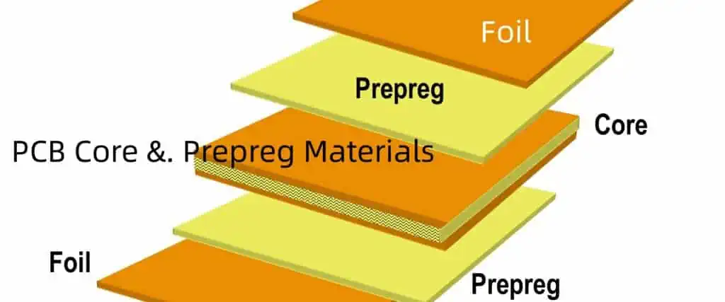
The foundation of a multilayer PCB is the core and prepreg materials. The core is a rigid, double-sided copper-clad laminate that forms the inner layers of the PCB. The prepreg, on the other hand, is a semi-cured, resin-impregnated glass-fiber material that is used to bond the core layers together during the lamination process.
Core Materials
The core materials used in multilayer PCB fabrication are typically made of a dielectric substrate, such as fiberglass-reinforced epoxy (FR-4), polyimide, or ceramic, with copper foil laminated on both sides. These core materials provide the mechanical support and electrical insulation necessary for the circuit traces and components.
The selection of the core material is crucial, as it must meet specific requirements, such as:
- Dielectric constant (Dk) and dissipation factor (Df) for signal integrity
- Thermal conductivity for heat dissipation
- Dimensional stability for reliable interconnections
- Chemical resistance to withstand the fabrication processes
Table 1 provides a comparison of common core materials used in multilayer PCB fabrication:
| Material | Dielectric Constant (Dk) | Dissipation Factor (Df) | Thermal Conductivity (W/m-K) |
|---|---|---|---|
| FR-4 | 4.2 – 4.7 | 0.017 – 0.020 | 0.3 – 0.4 |
| Polyimide | 3.4 – 3.8 | 0.002 – 0.004 | 0.4 – 0.6 |
| Ceramic | 3.8 – 9.8 | 0.001 – 0.003 | 20 – 40 |
Prepreg Materials
The prepreg materials used in multilayer PCB fabrication are typically made of a woven glass-fiber mat impregnated with a thermosetting resin, such as epoxy or polyimide. The prepreg acts as an adhesive layer that bonds the core layers together during the lamination process.
The selection of the prepreg material is crucial, as it must have the following properties:
- Suitable dielectric properties to maintain signal integrity
- Appropriate flow and melt viscosity for uniform bonding
- Thermal stability to withstand the high temperatures during fabrication
- Chemical resistance to withstand the various chemicals used in the process
Table 2 provides a comparison of common prepreg materials used in multilayer PCB fabrication:
| Material | Dielectric Constant (Dk) | Dissipation Factor (Df) | Resin Flow |
|---|---|---|---|
| Epoxy Prepreg | 4.0 – 4.5 | 0.015 – 0.020 | Medium |
| Polyimide Prepreg | 3.2 – 3.6 | 0.002 – 0.004 | Low |
| Cyanate Ester Prepreg | 3.0 – 3.4 | 0.005 – 0.008 | Medium |
Drilling and Plating
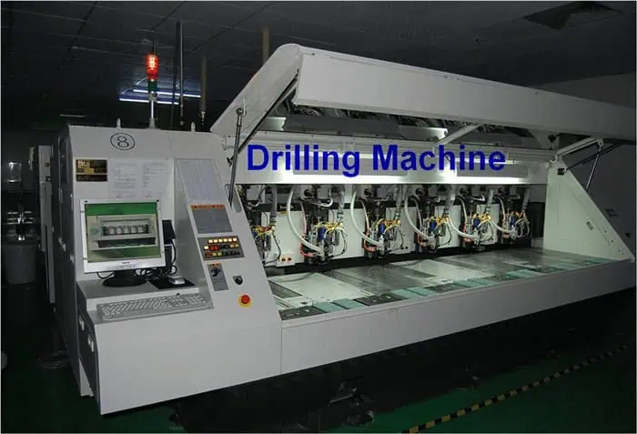
After the core and prepreg materials have been prepared, the next step in the multilayer PCB fabrication process is drilling and plating.
Drilling
The drilling process involves the creation of vias, which are holes that provide electrical interconnections between the different layers of the PCB. These vias can be classified into two main types:
- Plated-through Holes (PTHs): These are holes that are drilled through the entire thickness of the PCB and are subsequently plated with a conductive material, typically copper, to create an electrical connection between the layers.
- Blind Vias: These are holes that are drilled and plated, but do not extend through the entire thickness of the PCB. They are used to connect specific layers within the multilayer structure.
The drilling process requires precise control over the hole size, location, and depth to ensure reliable interconnections and maintain the overall structural integrity of the PCB.
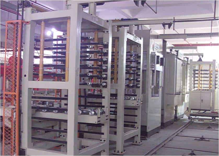
Plating
After the drilling process, the vias are plated with a conductive material, typically copper, to create the electrical connections between the layers. This plating process involves several steps:
- Desmearing: The inner walls of the drilled holes are chemically treated to remove any resin residue, ensuring a clean surface for the plating process.
- Catalyzation: A catalytic layer, such as palladium, is deposited on the inner walls of the holes to facilitate the subsequent electroplating process.
- Electroplating: Copper is electrochemically deposited on the inner walls of the holes, creating a continuous conductive path between the layers.
- Copper Thickness Adjustment: The copper thickness on the inner walls of the vias is adjusted to meet the design specifications, typically ranging from 15 to 35 microns.
The plating process is crucial for ensuring reliable electrical connections and maintaining the overall structural integrity of the multilayer PCB.
Imaging and Etching

After the drilling and plating processes, the next step in the multilayer PCB fabrication process is imaging and etching.
Imaging
The imaging process involves the transfer of the circuit pattern onto the copper-clad layers of the PCB. This is typically done using one of the following methods:
- Photolithography: A photoresist material is applied to the copper-clad layers, and the circuit pattern is transferred using a photomask and UV light exposure.
- Direct Imaging: The circuit pattern is directly imaged onto the photoresist-coated copper layers using a high-resolution laser or DLP (Digital Light Processing) system, eliminating the need for a photomask.
The imaging process ensures that the desired circuit pattern is accurately transferred to the copper layers, providing the foundation for the subsequent etching process.
Etching
The etching process involves the selective removal of unwanted copper from the PCB layers, leaving behind the desired circuit patterns. This is typically done using a chemical etching process, where the exposed copper is dissolved by a chemical etchant, such as ferric chloride or ammoniacal copper etchant.
The etching process requires precise control over the etchant concentration, temperature, and exposure time to ensure the accurate reproduction of the circuit patterns and maintain the desired copper thickness.
After the etching process, the remaining photoresist is removed, leaving behind the desired circuit patterns on the PCB layers.
Multilayer Lamination
The next step in the multilayer PCB fabrication process is the lamination of the individual layers to form the final multilayer structure.
Lay-up
The lay-up process involves the stacking and alignment of the individual PCB layers, including the core, prepreg, and any additional layers, such as copper foils or solder masks. The layers are carefully aligned to ensure accurate positioning of the circuit patterns and vias.
Lamination
The lamination process involves the application of heat and pressure to bond the individual layers together, creating the multilayer PCB structure. During this process, the prepreg material melts and flows, filling any gaps between the layers and creating a strong, uniform bond.
The lamination process is typically performed in a hydraulic press or a vacuum lamination machine, with precise control over the temperature, pressure, and duration to ensure the optimal bonding of the layers.
Dimensional Stability
After the lamination process, the multilayer PCB undergoes a cooling phase to solidify the bond between the layers. During this cooling process, it is essential to maintain the dimensional stability of the PCB to ensure the accurate alignment of the circuit patterns and vias.
The dimensional stability of the multilayer PCB is influenced by factors such as the material properties of the core and prepreg, the lamination conditions, and the thermal management during the fabrication process.
Final Finishing and Inspection
The final stage of the multilayer PCB fabrication process involves the finishing steps and the inspection of the final product.
Final Finishing
The finishing steps include the following:
- Outer Layer Imaging and Etching: The outer layers of the multilayer PCB are imaged and etched to create the final circuit patterns.
- Surface Finishing: The exposed copper surfaces are treated with a protective coating, such as gold, silver, or tin-lead, to improve solderability and corrosion resistance.
- Solder Mask Application: A solder mask, a protective coating that prevents solder from bridging between circuit traces, is applied to the PCB.
- Silkscreen Printing: Alphanumeric markings and other surface legends are printed on the PCB using a silkscreen process.
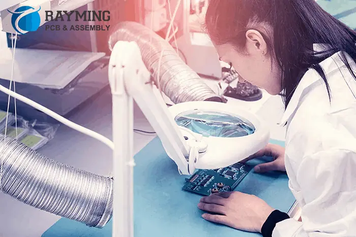
Inspection and Testing
The final multilayer PCB is thoroughly inspected and tested to ensure its quality and reliability. This includes:
- Visual Inspection: The PCB is visually inspected for any defects, such as scratches, misalignment, or surface blemishes.
- Electrical Testing: The PCB is tested for continuity, isolation, and other electrical parameters to ensure the integrity of the circuit connections.
- Mechanical Testing: The PCB is tested for physical properties, such as flex, twist, and thermal cycling, to ensure its structural integrity.
- Environmental Testing: The PCB may undergo additional environmental tests, such as temperature and humidity cycling, to assess its performance under various operating conditions.
Only after passing these rigorous inspection and testing procedures can the multilayer PCB be deemed ready for final assembly and integration into the end product.
FAQ

Q1: What are the key factors to consider when selecting core and prepreg materials for multilayer PCB fabrication?
A1: The key factors to consider when selecting core and prepreg materials include:
- Dielectric constant (Dk) and dissipation factor (Df) to maintain signal integrity
- Thermal conductivity for heat dissipation
- Dimensional stability for reliable interconnections
- Chemical resistance to withstand the fabrication processes
- Resin flow and melt viscosity for uniform bonding during lamination
Q2: What is the purpose of the desmearing process in the plating stage of multilayer PCB fabrication?
A2: The desmearing process is used to remove any resin residue from the inner walls of the drilled holes. This ensures a clean surface for the subsequent catalyzation and electroplating steps, which are crucial for creating reliable electrical connections between the layers of the multilayer PCB.
Q3: How does the choice of imaging method (photolithography vs. direct imaging) affect the multilayer PCB fabrication process?
A3: The choice of imaging method can have the following impact on the multilayer PCB fabrication process:
- Photolithography requires the use of a photomask, which adds an additional step and can affect the overall cost and turnaround time.
- Direct imaging eliminates the need for a photomask, simplifying the process and potentially reducing the cost and turnaround time.
- Direct imaging can also offer higher resolution and better registration accuracy, leading to improved circuit pattern transfer.
Q4: What are the key considerations during the lamination process to ensure the dimensional stability of the final multilayer PCB?
A4: The key considerations during the lamination process to ensure dimensional stability include:
- Precise control over temperature, pressure, and duration to optimize the bonding of the layers
- Careful selection of core and prepreg materials with compatible thermal expansion coefficients
- Effective thermal management during the cooling phase to minimize warping or shrinkage of the PCB
Q5: What are the common surface finishing options for multilayer PCBs, and how do they affect the PCB’s performance and reliability?
A5: The common surface finishing options for multilayer PCBs include:
- Gold: Provides excellent solderability and corrosion resistance, but is more expensive.
- Silver: Offers good solderability and conductivity, but is susceptible to oxidation.
- Tin-lead: A traditional option that provides good solderability and moderate corrosion resistance. The choice of surface finishing depends on the specific application requirements, such as soldering method, operating environment, and cost considerations.