“Turnkey” or “Consigned”…Which is the Better Choice to go for Electronics and Design Solutions..?

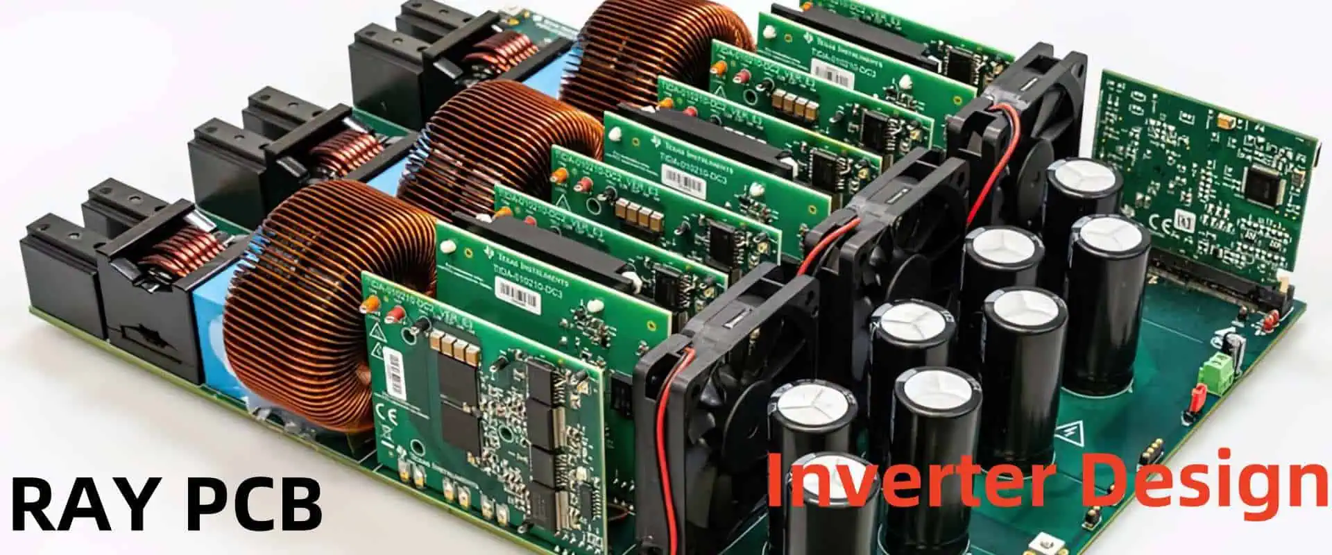
The Rise of Turnkey and Consigned Solutions

In the rapidly evolving world of electronics and design, businesses are constantly seeking efficient and cost-effective solutions to meet their ever-changing needs. Two popular approaches that have gained significant traction in recent years are the “turnkey” and “consigned” models. These two strategies offer distinct advantages and considerations, leaving many organizations to ponder the question: Which is the better choice for electronics and design solutions?

To delve deeper into this topic, let’s explore the key characteristics, benefits, and drawbacks of both the turnkey and consigned approaches.

Understanding Turnkey Solutions

A turnkey solution is a comprehensive package that provides a complete, ready-to-use system or service. In the context of electronics and design, a turnkey solution typically includes the following components:

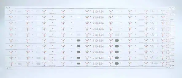
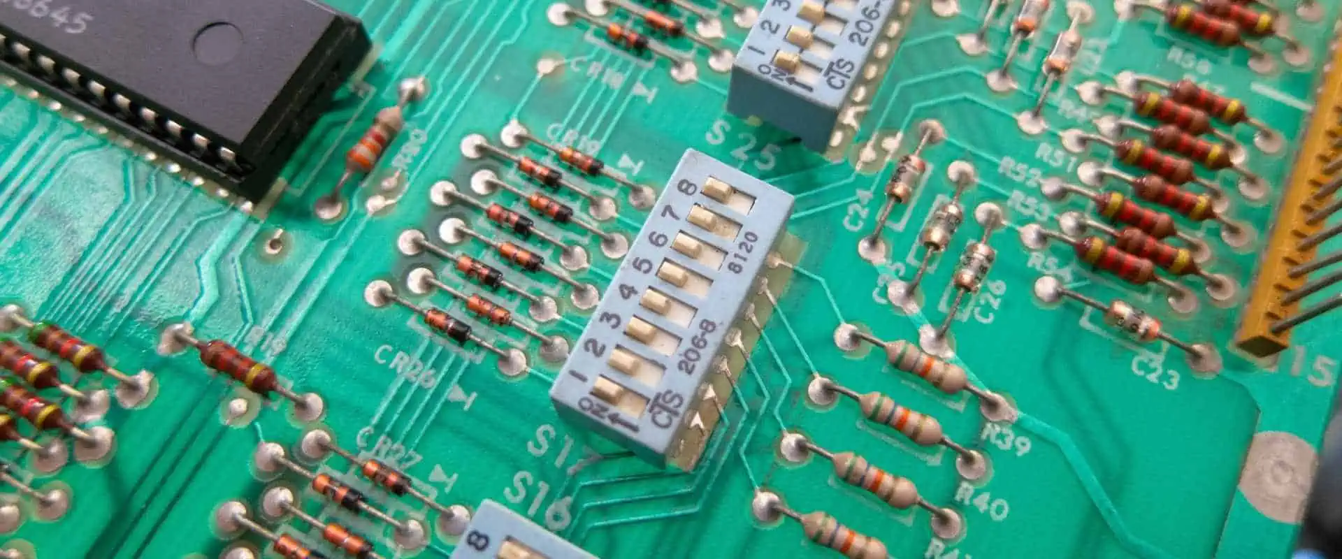
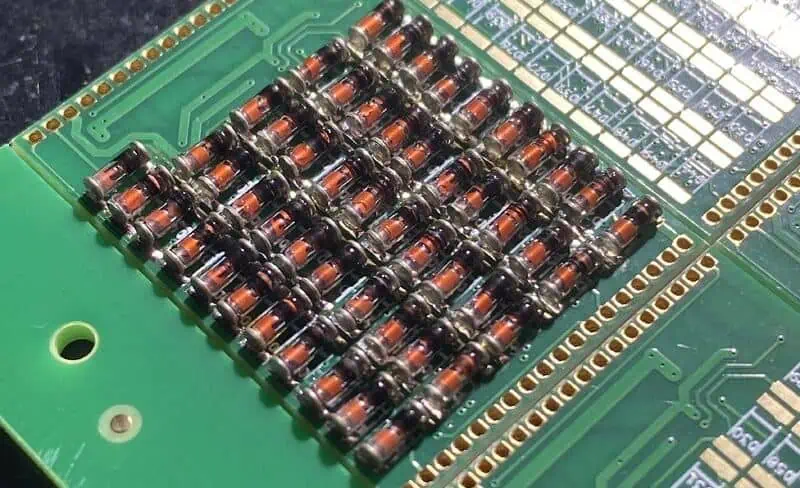
  1. Hardware: The physical components, such as circuit boards, microcontrollers, sensors, and other electronic devices, are sourced, assembled, and configured by the provider.
  2. Software: The necessary software, including firmware, operating systems, and any specialized applications, is pre-installed and tested by the provider.
  3. Integration: The hardware and software components are seamlessly integrated, ensuring a plug-and-play experience for the end-user.
  4. Support: The provider offers ongoing maintenance, technical support, and updates to ensure the smooth operation of the solution.

The key advantage of a turnkey solution is its convenience and ease of implementation. Businesses can simply “plug in” the solution and have it up and running with minimal effort and technical expertise required on their part. This approach is particularly appealing for organizations that lack in-house engineering resources or prefer to focus on their core competencies rather than managing the intricacies of electronics and design.

Advantages of Turnkey Solutions

  1. Reduced Time-to-Market: Turnkey solutions are designed to be quickly deployed, enabling businesses to accelerate their time-to-market and respond to market demands more efficiently.
  2. Minimized Risk: By outsourcing the design, development, and integration of the solution to the provider, businesses can minimize the technical risks and complexities associated with electronics and design projects.
  3. Improved Scalability: Turnkey solutions are often scalable, allowing businesses to easily expand or upgrade their systems as their needs evolve.
  4. Ongoing Support: Turnkey providers typically offer comprehensive support, including maintenance, troubleshooting, and updates, ensuring the long-term reliability and performance of the solution.

Potential Drawbacks of Turnkey Solutions

  1. Limited Customization: Turnkey solutions are designed to be “one-size-fits-all,” which may limit the ability to tailor the solution to specific business requirements or unique use cases.
  2. Vendor Lock-in: Businesses may become dependent on the turnkey provider, making it challenging to switch to alternative solutions or service providers in the future.
  3. Higher Upfront Costs: Turnkey solutions typically have higher initial costs compared to building or assembling the solution in-house.
  4. Ongoing Maintenance Costs: The ongoing support and maintenance provided by the turnkey provider can result in recurring costs that may be higher than managing the solution internally.

Understanding Consigned Solutions

In contrast to turnkey solutions, consigned solutions involve a more collaborative approach between the business and the service provider. In this model, the provider takes on the responsibility of sourcing, managing, and maintaining the electronic components and design elements, while the business retains ownership and control over the final product.

The key aspects of a consigned solution include:

  1. Component Sourcing: The provider is responsible for identifying, procuring, and managing the necessary electronic components, leveraging their expertise and established supply chain relationships.
  2. Inventory Management: The provider handles the storage, tracking, and replenishment of the electronic components, ensuring the availability of required parts.
  3. Assembly and Integration: The provider may assist with the assembly, testing, and integration of the electronic components, but the final product remains under the ownership and control of the business.
  4. Technical Support: The provider offers technical support, troubleshooting, and problem-solving assistance to the business, but the business retains the decision-making authority.

The consigned model is often preferred by organizations that have a strong in-house engineering or design team, but require specialized expertise or resources in specific areas of electronics and design.

Advantages of Consigned Solutions

  1. Customization: Consigned solutions allow for a higher degree of customization, as the business maintains control over the final product design and specifications.
  2. Cost Optimization: By leveraging the provider’s expertise and economies of scale, businesses can often achieve cost savings on component sourcing and inventory management.
  3. Reduced Capital Expenditure: With the consigned model, businesses can avoid the upfront investment in purchasing and maintaining electronic components, allowing them to redirect their capital towards other strategic priorities.
  4. Flexibility: The consigned approach offers more flexibility, as businesses can easily scale their operations, adjust component requirements, or switch providers if needed.

Potential Drawbacks of Consigned Solutions

  1. Increased Complexity: The collaborative nature of the consigned model requires ongoing communication, coordination, and clear delineation of responsibilities between the business and the provider.
  2. Potential Delays: Depending on the provider’s capacity and lead times, businesses may face occasional delays in the availability of components or the completion of assembly and integration tasks.
  3. Reliance on Provider: Businesses may become dependent on the expertise and reliability of the service provider, which could pose challenges if the provider experiences difficulties or changes in their operations.
  4. Potential for Misalignment: If the business and provider have different priorities or goals, it may lead to conflicts or misaligned expectations, which could impact the effectiveness of the consigned solution.

Comparing Turnkey and Consigned Solutions

To help businesses make an informed decision, let’s compare the key characteristics of turnkey and consigned solutions in a table format:

FeatureTurnkey SolutionConsigned Solution
OwnershipThe provider owns and manages the complete solution.The business retains ownership of the final product, while the provider manages the components and process.
CustomizationLimited customization options; the solution is more “one-size-fits-all.”Higher degree of customization, as the business maintains control over the design and specifications.
Time-to-MarketFaster deployment, as the solution is pre-configured and ready to use.Slightly longer lead times, as the provider may need to source and integrate components.
Risk ManagementThe provider bears the technical risks associated with the solution.The business retains some technical risks, but the provider mitigates risks related to component sourcing and inventory management.
Ongoing CostsHigher initial costs, but potentially lower ongoing maintenance and support costs.Lower initial costs, but ongoing costs for component management and provider services.
Vendor DependenceHigher degree of dependence on the turnkey provider.Some dependence on the provider, but the business maintains more control and flexibility.
Expertise RequiredLess in-house technical expertise required, as the provider handles the technical details.Requires in-house engineering or design expertise to work effectively with the provider.

Factors to Consider when Choosing Between Turnkey and Consigned Solutions

When deciding between a turnkey or consigned solution, businesses should carefully consider the following factors:

  1. Business Objectives and Requirements: Evaluate your specific business goals, the complexity of your electronics and design needs, and the level of customization required.
  2. In-house Capabilities: Assess your organization’s internal technical expertise, engineering resources, and the ability to manage the project lifecycle.
  3. Cost Considerations: Analyze the total cost of ownership, including initial investments, ongoing maintenance, and potential future upgrades or expansions.
  4. Risk Tolerance: Determine your organization’s risk appetite and the level of technical risk you’re willing to assume or transfer to the provider.
  5. Vendor Evaluation: Thoroughly research and evaluate potential providers, considering their track record, industry expertise, and ability to deliver on their promises.
  6. Scalability and Flexibility: Ensure the chosen solution can accommodate your business’s growth and adapt to changing market conditions or technological advancements.
  7. Integration and Compatibility: Evaluate how the solution will integrate with your existing systems, processes, and workflows.

Frequently Asked Questions (FAQs)

1. What are the key differences between turnkey and consigned solutions?

The main differences lie in the level of ownership, control, and customization. Turnkey solutions are fully owned and managed by the provider, offering a more “plug-and-play” approach, while consigned solutions involve a collaborative model where the business retains ownership and control over the final product.

2. Which solution is better for businesses with limited in-house technical expertise?

Turnkey solutions are generally more suitable for businesses with limited in-house technical expertise, as the provider handles the majority of the technical details and implementation. Consigned solutions require a higher degree of internal engineering or design capabilities to work effectively with the provider.

3. How do the costs compare between turnkey and consigned solutions?

Turnkey solutions typically have higher initial costs but potentially lower ongoing maintenance and support costs. Consigned solutions generally have lower upfront costs, but businesses may incur ongoing expenses for component management and provider services.

4. What are the advantages of a consigned solution for businesses with specialized requirements?

Consigned solutions offer a higher degree of customization, allowing businesses to tailor the electronics and design elements to their specific needs. This can be particularly beneficial for organizations with unique use cases or requirements that may not be well-suited for a standardized turnkey offering.

5. How do businesses mitigate the risks associated with turnkey and consigned solutions?

For turnkey solutions, the primary risk mitigation strategy is to thoroughly evaluate the provider’s capabilities, track record, and ability to deliver on their promises. For consigned solutions, clear communication, well-defined responsibilities, and a strong partnership between the business and the provider are crucial to managing risks effectively.

Conclusion

In the dynamic landscape of electronics and design, both turnkey and consigned solutions offer unique advantages and considerations. The choice between the two ultimately depends on your organization’s specific needs, resources, and strategic objectives.

Turnkey solutions provide a more convenient and risk-averse approach, particularly for businesses with limited technical expertise. Consigned solutions, on the other hand, offer greater customization and cost optimization opportunities for organizations with robust in-house engineering or design capabilities.

By carefully evaluating the factors discussed in this article, businesses can make an informed decision that aligns with their goals, resources, and long-term growth plans. Regardless of the chosen approach, partnering with a reliable and experienced provider is essential to ensure the successful implementation and ongoing success of your electronics and design solutions.

How to Design a SAFE, EFFICIENT, and COMPACT Inverter

Designing a safe, efficient, and compact inverter is a crucial task for engineers and electronics enthusiasts alike. Inverters are essential components in various applications, from renewable energy systems to industrial equipment, and their performance can significantly impact the overall system’s reliability and energy efficiency. In this comprehensive article, we will explore the key considerations and best practices for designing an inverter that meets these essential criteria.

Understanding the Fundamentals of Inverter Design

An inverter is a power electronic device that converts direct current (DC) to alternating current (AC). The primary function of an inverter is to transform the voltage and current characteristics of the input DC power to match the requirements of the AC load. Inverters can be classified into different types based on their input voltage, output voltage, and power rating.

In the context of safe, efficient, and compact inverter design, the following factors play a crucial role:

  1. Safety Considerations:
    • Overcurrent and overload protection
    • Thermal management and heatsink design
    • Isolation and grounding requirements
    • Compliance with safety standards (e.g., UL, IEC, NEC)
  2. Efficiency Optimization:
    • Selection of high-efficiency semiconductor devices
    • Minimizing power losses in various components
    • Optimization of switching frequency and modulation techniques
    • Thermal management and cooling system design
  3. Compact Design:
    • Miniaturization of components and circuit layout
    • Utilization of high-density packaging and integration techniques
    • Optimization of heat dissipation and thermal management

Safety Considerations in Inverter Design

Safety is of paramount importance when designing an inverter, as it directly impacts the reliability and longevity of the system. Let’s delve into the key safety aspects that should be addressed during the design process.

Overcurrent and Overload Protection

Inverters are susceptible to overcurrent and overload conditions, which can lead to component failure and even fire hazards. To mitigate these risks, the inverter design must incorporate effective overcurrent and overload protection mechanisms, such as:

  • Circuit Breakers: Incorporating circuit breakers that can quickly interrupt the flow of current in the event of an overload or short circuit.
  • Fuses: Using fast-acting fuses to protect the inverter’s internal components from excessive current.
  • Current Limiting Circuitry: Implementing current limiting circuitry to prevent the inverter from delivering more current than the system can safely handle.

Thermal Management and Heatsink Design

Inverters generate heat during operation due to power losses in various components, such as semiconductor devices, control circuitry, and passive components. Effective thermal management is crucial to ensure the safe and reliable operation of the inverter. This includes:

  • Heatsink Design: Designing an efficient heatsink that can effectively dissipate the heat generated by the inverter’s components.
  • Air or Liquid Cooling: Incorporating active cooling systems, such as fans or liquid cooling, to enhance heat dissipation.
  • Thermal Monitoring: Implementing temperature sensors and control algorithms to monitor and manage the inverter’s thermal performance.

Isolation and Grounding Requirements

Proper isolation and grounding are essential for the safety of the inverter and the connected system. This includes:

  • Input-Output Isolation: Ensuring adequate isolation between the input DC side and the output AC side to prevent the transfer of dangerous voltages.
  • Grounding and Bonding: Establishing a robust grounding and bonding system to protect against electric shock and ensure the integrity of the system’s electrical safety.
  • Compliance with Standards: Designing the inverter to meet the requirements of relevant safety standards, such as UL, IEC, and NEC, to ensure the overall system’s safety and compliance.

Efficiency Optimization in Inverter Design

Efficiency is a critical aspect of inverter design, as it directly impacts the energy consumption, operating costs, and environmental impact of the system. Here are the key considerations for optimizing the efficiency of an inverter:

Selection of High-Efficiency Semiconductor Devices

The choice of semiconductor devices, such as power transistors and diodes, plays a significant role in the overall efficiency of the inverter. Factors to consider include:

  • Switch Selection: Selecting high-efficiency semiconductor switches, such as MOSFETs or IGBTs, that exhibit low on-state resistance and switching losses.
  • Diode Selection: Choosing low-loss diodes, such as Schottky or ultra-fast recovery diodes, to minimize conduction and switching losses.

Minimizing Power Losses in Various Components

Reducing power losses in the inverter’s various components, such as the input filter, output filter, and control circuitry, can significantly improve the overall efficiency. Strategies include:

  • Optimizing Filter Design: Designing the input and output filters to minimize conduction and switching losses.
  • Minimizing Winding Losses: Optimizing the design of transformers and inductors to reduce copper and core losses.
  • Reducing Capacitor Losses: Selecting low-loss capacitors and minimizing the number of capacitors used in the inverter circuit.

Optimization of Switching Frequency and Modulation Techniques

The switching frequency and modulation technique employed in the inverter can have a significant impact on efficiency. Factors to consider include:

  • Switching Frequency: Selecting an optimum switching frequency that balances switching losses and filter requirements.
  • Modulation Techniques: Utilizing advanced modulation techniques, such as PWM (Pulse-Width Modulation) or SVM (Space Vector Modulation), to minimize harmonic distortion and improve efficiency.

Thermal Management and Cooling System Design

Effective thermal management is crucial for maintaining the inverter’s efficiency. This includes:

  • Heatsink Design: Designing an efficient heatsink that can effectively dissipate the heat generated by the inverter’s components.
  • Active Cooling Systems: Incorporating active cooling systems, such as fans or liquid cooling, to enhance heat dissipation and maintain optimal operating temperatures.
  • Thermal Monitoring and Control: Implementing temperature sensors and control algorithms to monitor and manage the inverter’s thermal performance, ensuring that it operates within the optimal temperature range.

Compact Design of Inverters

Compact inverter design is essential in applications where space is limited, such as in portable electronics, renewable energy systems, or industrial equipment. Achieving a compact design requires optimization of both the physical layout and the integration of components. Let’s explore the key strategies for compact inverter design:

Miniaturization of Components and Circuit Layout

Reducing the physical size of the inverter’s components and optimizing the circuit layout can significantly contribute to a compact design. Strategies include:

  • Component Selection: Choosing compact, high-density components, such as surface-mount devices (SMDs) and integrated circuits (ICs), to minimize the overall footprint.
  • Circuit Layout Optimization: Employing techniques like high-density PCB design, multilayer boards, and component placement optimization to minimize the overall size of the inverter.

Utilization of High-Density Packaging and Integration Techniques

Advanced packaging and integration techniques can further enhance the compactness of the inverter design. These include:

  • Power Modules: Integrating multiple power semiconductor devices, control circuitry, and other components into a single power module to reduce the overall size and complexity of the inverter.
  • System-on-Chip (SoC) Integration: Integrating the inverter’s control, driver, and power conversion functions into a single integrated circuit (IC) to achieve a highly compact and integrated design.
  • Multifunctional Components: Utilizing components that combine multiple functions, such as integrated gate drivers or multiphase converters, to reduce the overall component count and footprint.

Optimization of Heat Dissipation and Thermal Management

Effective thermal management is crucial in compact inverter designs, as the limited physical space can challenge the ability to dissipate heat efficiently. Strategies for optimizing heat dissipation and thermal management include:

  • Heatsink Integration: Designing the heatsink as an integral part of the inverter’s physical structure to maximize heat dissipation while maintaining a compact form factor.
  • Thermal Interface Materials: Using high-performance thermal interface materials, such as thermal greases or phase-change materials, to improve the thermal coupling between components and the heatsink.
  • Airflow Optimization: Optimizing the airflow and cooling system design to efficiently remove heat from the inverter’s critical components, even in a compact enclosure.

Case Study: Designing a Compact, High-Efficiency Inverter for a Solar PV System

To illustrate the practical application of the principles discussed, let’s consider a case study of designing a compact, high-efficiency inverter for a solar photovoltaic (PV) system.

System Requirements

  • Input Voltage: 48 VDC (from solar PV array)
  • Output Voltage: 230 VAC, 50 Hz
  • Power Rating: 5 kW

Safety Considerations

  • Overcurrent and overload protection: Implement a circuit breaker and fast-acting fuses to protect against overcurrent and overload conditions.
  • Thermal management: Design a heatsink with a high-efficiency air cooling system to dissipate the heat generated by the inverter’s components.
  • Isolation and grounding: Ensure proper input-output isolation and establish a robust grounding system to meet safety standards.

Efficiency Optimization

  • Semiconductor device selection: Choose high-efficiency MOSFETs and Schottky diodes to minimize conduction and switching losses.
  • Input and output filter design: Optimize the filter design to reduce conduction and switching losses.
  • Switching frequency and modulation: Employ a PWM modulation technique with a switching frequency of 20 kHz to balance efficiency and filter requirements.
  • Thermal management: Integrate the heatsink design with the overall inverter layout to efficiently dissipate heat.

Compact Design Strategies

  • Component miniaturization: Utilize SMD components and high-density PCB design to minimize the physical footprint.
  • Integrated power module: Employ a compact power module that integrates the power semiconductor devices, gate drivers, and control circuitry.
  • Heatsink integration: Design the heatsink as an integral part of the inverter’s enclosure to maximize heat dissipation while maintaining a compact form factor.
  • Airflow optimization: Optimize the cooling system design to ensure efficient heat removal from the critical components, even in a compact enclosure.

By implementing the safety, efficiency, and compactness principles discussed in this article, the resulting inverter design for the solar PV system would be a compact, high-efficiency, and safe solution, suitable for integration into a space-constrained renewable energy application.

FAQ (Frequently Asked Questions)

  1. What are the key considerations for designing a safe inverter?
    • Overcurrent and overload protection
    • Thermal management and heatsink design
    • Isolation and grounding requirements
    • Compliance with safety standards (e.g., UL, IEC, NEC)
  2. How can I optimize the efficiency of an inverter design?
    • Select high-efficiency semiconductor devices
    • Minimize power losses in various components
    • Optimize switching frequency and modulation techniques
    • Implement effective thermal management and cooling systems
  3. What strategies can be used to achieve a compact inverter design?
    • Miniaturize components and optimize circuit layout
    • Utilize high-density packaging and integration techniques
    • Optimize heat dissipation and thermal management
  4. How does the selection of semiconductor devices impact the efficiency of an inverter?
    • The choice of power transistors (e.g., MOSFETs, IGBTs) and diodes with low on-state resistance and switching losses can significantly improve the overall efficiency of the inverter.
  5. What are the benefits of using a power module in a compact inverter design?
    • Power modules integrate multiple power semiconductor devices, control circuitry, and other components into a single package, reducing the overall size and complexity of the inverter design.

PCB Layout Optimization for LED Backlight Module

Backlightย PCB

In the rapidly evolving world of display technology, the LED backlight module has emerged as a crucial component, responsible for delivering vibrant and energy-efficient illumination to a wide range of electronic devices, from smartphones and tablets to TVs and computer monitors. As the demand for these displays continues to grow, the optimization of the printed circuit board (PCB) layout for LED backlight modules has become increasingly important, as it directly impacts the performance, reliability, and cost-effectiveness of the final product.

The PCB layout for an LED backlight module involves the careful arrangement of various components, including the LED chips, driver circuitry, and supporting electronics, to ensure optimal light distribution, heat dissipation, and overall system efficiency. This process requires a deep understanding of electromagnetic principles, thermal management, and circuit design, as well as a keen attention to detail and a well-structured design approach.

In this comprehensive article, we will delve into the key aspects of PCB layout optimization for LED backlight modules, providing insights and best practices that can help designers and engineers achieve superior performance and reliability in their products.

Understanding LED Backlight Module Design

LED Chip Placement and Arrangement

The placement and arrangement of the LED chips within the backlight module play a crucial role in determining the overall light output, uniformity, and efficiency of the system. Factors such as the number of LEDs, their spatial distribution, and the distance between them can significantly impact the final light output and its distribution across the display surface.

One common approach is to arrange the LEDs in a grid-like pattern, with evenly spaced rows and columns, to ensure a consistent and uniform light distribution. However, more advanced designs may also incorporate specific patterns or arrangements to address specific design challenges, such as hot spots, edge effects, or the need for higher brightness in certain regions of the display.

Factors Affecting LED Chip Placement

  1. Light Output and Uniformity: The placement of LEDs directly affects the overall light output and the uniformity of the illumination across the display surface. Careful arrangement can help minimize dark spots and hot spots, ensuring a consistent and visually pleasing appearance.
  2. Heat Management: The placement of LEDs must also consider the thermal management of the system. LEDs generate heat during operation, and the layout should ensure efficient heat dissipation to maintain the desired performance and lifespan of the LEDs.
  3. Optical Design: The layout of the LEDs should complement the optical design of the backlight module, which may include the use of diffusers, reflectors, or other optical elements to shape and control the light output.
  4. Electrical Design: The electrical connections between the LEDs and the driver circuitry must be carefully considered, as the layout can impact the overall efficiency, power consumption, and potential for electromagnetic interference (EMI).

Driver Circuit Design and Layout

The driver circuit is responsible for providing the necessary power and control signals to the LED chips, ensuring their proper operation and performance. The layout of the driver circuit on the PCB can have a significant impact on the overall efficiency, reliability, and electromagnetic compatibility (EMC) of the LED backlight module.

Key Considerations for Driver Circuit Layout

  1. Power Distribution: Efficient power distribution is crucial to ensure uniform current delivery to all LED chips, minimizing voltage drops and ensuring consistent brightness across the display.
  2. Heat Management: The driver circuit components, such as power MOSFETs and voltage regulators, generate heat during operation, and their placement and layout should consider efficient heat dissipation.
  3. EMI/EMC: The layout of the driver circuit must be designed to minimize electromagnetic interference (EMI) and ensure electromagnetic compatibility (EMC) with other electronic components in the system.
  4. Decoupling and Filtering: Proper decoupling and filtering of the power supply lines are essential to maintain signal integrity and prevent noise and ripple from affecting the LED operation.
  5. Feedback and Control Circuits: The layout of the feedback and control circuits, such as current sensing and dimming control, can impact the overall performance and stability of the LED backlight module.

Thermal Management Considerations

Thermal management is a critical aspect of PCB layout optimization for LED backlight modules, as the LEDs and associated electronic components generate significant amounts of heat during operation. Proper thermal design can help ensure the reliable and long-term operation of the LED backlight module, as well as maintain the desired brightness and color consistency.

Key Thermal Management Strategies

  1. Heat Sink Design: The PCB layout should incorporate an efficient heat sink design, which may include the use of copper planes, thermal vias, or dedicated heat dissipation structures, to effectively transfer heat away from the LED chips and other heat-generating components.
  2. Component Placement: The placement of components on the PCB, such as the LEDs, driver circuits, and other heat-generating devices, should be carefully considered to optimize heat dissipation and prevent thermal hotspots.
  3. Air Flow and Ventilation: The PCB layout should consider the overall airflow and ventilation within the LED backlight module, ensuring that adequate cooling is provided to the critical components.
  4. Thermal Simulation and Analysis: Thermal simulation and analysis tools can be invaluable in identifying potential thermal bottlenecks and optimizing the PCB layout for improved heat dissipation.
  5. Material Selection: The choice of materials used in the PCB, such as the copper weight and the dielectric layers, can also impact the thermal performance of the LED backlight module.

PCB Design Considerations for LED Backlight Modules

Multilayer PCB Design

Multilayer PCBs are commonly used in LED backlight module designs due to their ability to accommodate complex routing, power distribution, and thermal management requirements. The number of layers and their specific functions can vary based on the complexity of the design and the performance requirements of the LED backlight module.

Key Advantages of Multilayer PCB Design

  1. Power Distribution: Multilayer PCBs allow for the creation of dedicated power and ground planes, ensuring efficient power distribution to the LED chips and other electronic components.
  2. Signal Integrity: The use of inner layers for signal routing can help improve signal integrity by providing better control over impedance, crosstalk, and electromagnetic interference (EMI).
  3. Thermal Management: The additional layers in a multilayer PCB can be utilized for heat dissipation, either through the use of copper planes or the incorporation of thermal vias.
  4. Component Placement: Multilayer PCBs offer more flexibility in component placement, allowing for efficient layout optimization and improved overall system performance.
  5. Complexity and Integration: Multilayer PCBs enable the integration of more complex circuitry and components within a compact form factor, which is particularly important for LED backlight modules in space-constrained applications.

Considerations in Multilayer PCB Design

  1. Layer Stack-up: The selection of the appropriate layer stack-up, including the number of layers, their thickness, and the materials used, is crucial for optimizing the PCB’s performance and cost-effectiveness.
  2. Power and Ground Planes: The design and placement of power and ground planes are critical for ensuring efficient power distribution and minimizing noise and EMI.
  3. Signal Routing: Careful signal routing, including the use of controlled impedance traces, can help maintain signal integrity and minimize crosstalk and other electromagnetic interference.
  4. Thermal Management: The incorporation of thermal vias, copper planes, and other thermal management features can help ensure efficient heat dissipation and prevent thermal hotspots.
  5. Manufacturing Considerations: The selected multilayer PCB design should take into account the capabilities and limitations of the manufacturing process, ensuring that the design is both technically and economically feasible.

Copper Plane Design and Utilization

Copper planes play a crucial role in the PCB layout optimization for LED backlight modules, as they serve multiple purposes, including power distribution, ground reference, and thermal management.

Key Functions of Copper Planes

  1. Power Distribution: Dedicated power planes ensure efficient and uniform power delivery to the LED chips and other electronic components, minimizing voltage drops and ensuring consistent performance.
  2. Ground Reference: Ground planes provide a low-impedance reference for signal routing and help to reduce electromagnetic interference (EMI) and signal integrity issues.
  3. Thermal Management: Copper planes, especially those connected to ground, can serve as effective heat spreaders, aiding in the dissipation of heat generated by the LED chips and other components.
  4. Signal Integrity: Properly designed copper planes can help maintain signal integrity by providing a stable reference for high-speed signals and minimizing crosstalk.

Considerations in Copper Plane Design

  1. Plane Arrangement: The placement and arrangement of power and ground planes within the multilayer PCB should be carefully considered to optimize power distribution, thermal management, and signal integrity.
  2. Plane Partitioning: In some cases, it may be necessary to partition the copper planes to isolate different power domains or to address specific design requirements, such as the need for separate analog and digital ground planes.
  3. Plane Thickness: The thickness of the copper planes can impact their electrical and thermal performance, and should be selected based on the specific requirements of the LED backlight module design.
  4. Thermal Vias: The incorporation of thermal vias can help improve the heat transfer between the copper planes and the LED chips or other heat-generating components, enhancing the overall thermal management of the system.
  5. Manufacturing Considerations: The design of the copper planes should take into account the capabilities and limitations of the manufacturing process, ensuring that the final PCB can be fabricated reliably and cost-effectively.

Trace Design and Routing

The design and routing of the traces on the PCB can have a significant impact on the performance, reliability, and cost-effectiveness of the LED backlight module. Careful consideration must be given to factors such as current-carrying capacity, impedance control, and electromagnetic compatibility (EMC).

Key Considerations in Trace Design and Routing

  1. Current-Carrying Capacity: The traces carrying the LED driving current must be designed with sufficient width and copper weight to handle the required current without excessive heating or voltage drops.
  2. Impedance Control: For high-speed signals, such as those used in the driver circuitry, the trace design should ensure controlled impedance to maintain signal integrity and prevent reflections.
  3. Trace Spacing and Clearance: The spacing between traces and the clearance between traces and other components or plane edges must be carefully considered to prevent arcing, shorting, or electromagnetic interference.
  4. Trace Length Matching: In some applications, such as those with differential signaling, it may be necessary to match the lengths of the traces to ensure proper signal propagation and timing.
  5. Thermal Management: The routing of traces should consider the thermal aspects of the design, ensuring that heat-generating components are not placed in close proximity to sensitive traces or vias.
  6. EMC and EMI: The trace design and routing should also address electromagnetic compatibility (EMC) and electromagnetic interference (EMI) concerns, minimizing the potential for noise and interference within the LED backlight module and with other electronic systems.
  7. Manufacturing Considerations: The trace design should take into account the capabilities and limitations of the PCB manufacturing process, ensuring that the final design can be fabricated reliably and cost-effectively.

Component Placement and Orientation

The placement and orientation of components on the PCB can have a significant impact on the overall performance, thermal management, and manufacturability of the LED backlight module.

Key Considerations in Component Placement and Orientation

  1. Thermal Management: The placement of heat-generating components, such as LED chips and power electronics, should consider the efficient dissipation of heat and the prevention of thermal hotspots.
  2. Signal Integrity: The placement and orientation of sensitive components, such as driver ICs and control circuitry, should minimize the length of high-speed traces and prevent potential interference or crosstalk.
  3. Power Distribution: The placement of power-related components, such as power planes, decoupling capacitors, and voltage regulators, should ensure efficient and uniform power delivery to the LED chips and other electronic components.
  4. Manufacturability: The component placement should consider the manufacturing processes, such as pick-and-place and reflow soldering, to ensure reliable and cost-effective assembly.
  5. Accessibility and Testability: The placement of components should consider the accessibility for assembly, inspection, and testing, ensuring that the final product can be easily manufactured and serviced.
  6. Symmetry and Aesthetics: In some applications, the placement and orientation of components may also need to consider the overall symmetry and aesthetic appearance of the LED backlight module.

PCB Stackup and Layer Assignment

The PCB stackup and layer assignment are critical design decisions that can significantly impact the performance, cost, and manufacturability of the LED backlight module.

Key Considerations in PCB Stackup and Layer Assignment

  1. Power and Ground Planes: The allocation of dedicated power and ground planes is essential for efficient power distribution and noise reduction.
  2. Signal Routing: The assignment of layers for signal routing can help optimize signal integrity, minimize crosstalk, and address electromagnetic interference (EMI) concerns.
  3. Thermal Management: The incorporation of thermal management features, such as copper planes and thermal vias, can be facilitated through the PCB stackup design.
  4. Impedance Control: The PCB stackup can be designed to ensure controlled impedance for high-speed signals, such as those used in driver circuitry.
  5. Layer Count and Manufacturing Constraints: The selection of the appropriate layer count should balance the design requirements with the manufacturing capabilities and cost considerations.
  6. Material Selection: The choice of dielectric materials and their properties, such as dielectric constant and loss tangent, can impact the electrical and thermal performance of the PCB.
  7. Mechanical Considerations: The PCB stackup and layer assignment should also consider the mechanical requirements, such as rigidity, flexibility, or the need for cutouts or mounting holes.

Electromagnetic Interference (EMI) and Electromagnetic Compatibility (EMC) Considerations

Electromagnetic interference (EMI) and electromagnetic compatibility (EMC) are critical aspects of PCB layout optimization for LED backlight modules, as they can impact the overall performance, reliability, and compliance with regulatory standards.

Key EMI and EMC Considerations

  1. Power Supply and Decoupling: Proper power supply design and the use of decoupling capacitors can help mitigate conducted EMI issues.
  2. Trace Design and Routing: The design and routing of traces, particularly for high-speed signals, can impact radiated EMI and signal integrity.
  3. Grounding and Shielding: The use of ground planes, ground vias, and shielding can help contain and suppress electromagnetic interference.
  4. Component Placement: The placement and orientation of components, especially high-speed digital and power electronics, can affect EMI and EMC performance.
  5. Regulatory Compliance: The PCB layout must be designed to comply with relevant EMI and EMC standards, such as FCC, CE, or CISPR, to ensure the product can be safely and legally marketed.
  6. Simulation and Testing: Electromagnetic simulation tools and EMI/EMC testing during the design process can help identify and address potential issues early on.

Thermal Management Strategies

Effective thermal management is crucial for the reliable operation and long-term performance of LED backlight modules. The PCB layout plays a significant role in the thermal design, and several strategies can be employed to optimize heat dissipation.

Thermal Management Techniques

  1. Copper Planes and Thermal Vias: Utilizing thick copper planes and incorporating thermal vias can enhance heat transfer from the LED chips and other heat-generating components to the surrounding layers and the heat sink.
  2. Component Placement and Orientation: Careful placement and orientation of heat-generating components, such as LED chips and power electronics, can improve airflow and optimize heat dissipation.
  3. Heatsink Integration: Designing the PCB layout to facilitate the integration of a dedicated heatsink or heat spreader can significantly improve the overall thermal management of the LED backlight module.
  4. Thermal Simulation and Analysis: The use of thermal simulation tools and analysis techniques can help identify potential hot spots and guide the optimization of the PCB layout for effective heat dissipation.
  5. Material Selection: The choice of materials, such as the dielectric layers and the copper weight, can impact the thermal performance of the PCB and the overall thermal management of the LED backlight module.
  6. Airflow and Ventilation: Considering the overall airflow and ventilation within the LED backlight module can help ensure that adequate cooling is provided to the critical components.

Manufacturability and Cost Considerations

In addition to the technical performance requirements, the PCB layout for LED backlight modules must also consider the manufacturing processes and associated costs to ensure the product’s commercial viability.

Manufacturability and Cost-Effective Design

  1. PCB Complexity: The complexity of the PCB design, in terms of the number of layers, component density, and trace routing, can impact the manufacturing cost and yield.
  2. Component Selection: The choice of components, such as the LED chips, driver ICs, and passive components, can significantly affect the overall cost of the LED backlight module.
  3. Assembly Processes: The PCB layout should be designed to accommodate efficient assembly processes, such as surface mount technology (SMT) and automated soldering, to minimize labor costs and improve production throughput.
  4. Testing and Inspection: The PCB layout should facilitate easy access for testing and inspection, ensuring that the final product meets the required quality standards.
  5. Standardization and Modularization: Adopting standardized design approaches and modular architectures can help reduce the overall cost and improve the scalability of the LED backlight module production.
  6. Supplier Collaboration: Close collaboration with PCB manufacturers and component suppliers can help identify cost-effective design strategies and leverage their expertise in the optimization process.

How to Protect Your PCB Design From Manufacturers

In today’s highly competitive electronics industry, protecting your intellectual property (IP) is paramount. As a hardware designer, your printed circuit board (PCB) designs are valuable assets that represent countless hours of research, development, and innovation. Unfortunately, the manufacturing process often exposes these designs to potential theft or unauthorized replication. This article aims to provide comprehensive guidance on safeguarding your PCB designs from unscrupulous manufacturers, ensuring the integrity of your IP and the long-term success of your business.

Understanding the Risks

Before delving into the protective measures, it’s crucial to understand the potential risks associated with PCB manufacturing outsourcing. Here are some common scenarios that highlight the importance of design protection:

  1. Unauthorized Replication: A manufacturer might attempt to replicate your PCB design without your consent, producing counterfeit products for their own gain or reselling the design to third parties.
  2. Reverse Engineering: Skilled engineers at the manufacturing facility could reverse engineer your PCB design, gaining access to your proprietary technology and trade secrets.
  3. Design Theft: In some cases, unethical employees or contractors may intentionally steal your PCB design files and sell them to competitors or use them for personal gain.
  4. Intellectual Property Infringement: Inadequate protection measures can lead to patent, copyright, or trademark infringement, resulting in costly legal disputes and damage to your brand reputation.
  5. Loss of Competitive Advantage: If your PCB design falls into the wrong hands, your competitors may gain an unfair advantage by leveraging your hard work and innovation.

These risks underscore the importance of implementing robust protection strategies to safeguard your PCB designs throughout the manufacturing process.

Protecting Your PCB Design

Protecting your PCB design involves a multi-faceted approach that addresses various stages of the design and manufacturing process. Here are some effective strategies to consider:

1. Non-Disclosure Agreements (NDAs)

Before engaging with a PCB manufacturer, it’s crucial to have a well-crafted non-disclosure agreement (NDA) in place. An NDA is a legally binding contract that prohibits the manufacturer from disclosing or misusing your confidential information, including PCB design files, schematics, and other proprietary data.

Ensure that the NDA covers the following key aspects:

  • Clear definition of confidential information
  • Limitations on the use and disclosure of confidential information
  • Obligations to protect confidential information
  • Duration of the agreement and provisions for termination
  • Remedies and penalties for breaches of the agreement

It’s advisable to have your legal counsel review the NDA to ensure it meets your specific needs and complies with applicable laws and regulations.

2. Intellectual Property Protection

Protecting your intellectual property (IP) through patents, copyrights, and trademarks is essential for safeguarding your PCB designs. Here are some strategies to consider:

Patents

patents can protect the novel and non-obvious aspects of your PCB design, including circuit layouts, mechanical structures, and innovative features. By obtaining patents, you gain exclusive rights to your invention, deterring others from unauthorized use or replication.

Copyrights

Copyrights can protect the creative aspects of your PCB design, such as schematics, artwork, and technical documentation. While copyrights do not protect the functional aspects of your design, they can prevent others from reproducing or distributing your copyrighted materials without permission.

Trademarks

Trademarks can protect the branding elements of your PCB design, such as product names, logos, and distinctive markings. By registering trademarks, you can prevent others from using confusingly similar marks, ensuring consumer recognition and brand protection.

3. Data Security Measures

Implementing robust data security measures is crucial to prevent unauthorized access to your PCB design files. Here are some recommended practices:

Encryption

Encrypt all PCB design files, schematics, and related documentation before sharing them with the manufacturer. Use industry-standard encryption algorithms and strong encryption keys to ensure data confidentiality.

Access Controls

Implement strict access controls to limit access to your PCB design files. Only authorized personnel should have access to sensitive information, and access should be granted on a need-to-know basis.

Secure File Transfer

When transferring PCB design files to the manufacturer, use secure file transfer protocols (SFTP) or encrypted file-sharing platforms. Avoid sending sensitive data via unsecured email or file-sharing services.

Regular Audits and Monitoring

Conduct regular audits and monitoring of your data security measures to identify and address any potential vulnerabilities. Keep logs of all file transfers and access attempts to detect any suspicious activity.

4. Obfuscation Techniques

Obfuscation techniques can make it more challenging for unauthorized individuals to reverse engineer or understand your PCB design. Here are some strategies to consider:

Circuit Obfuscation

Employ circuit obfuscation techniques, such as adding dummy components, rerouting traces, or using camouflaging techniques, to obscure the actual functionality of your PCB design.

Firmware Encryption

If your PCB design includes firmware or embedded software, encrypt the firmware files to prevent unauthorized access or modification.

Design Watermarking

Embed digital watermarks or unique identifiers within your PCB design files, schematics, or documentation. These watermarks can help prove ownership and track unauthorized copies if your design is leaked or misused.

5. Manufacturing Process Controls

Implement stringent controls during the PCB manufacturing process to minimize the risk of design theft or unauthorized replication. Here are some recommendations:

Secure Manufacturing Facilities

Choose a reputable PCB manufacturer with secure manufacturing facilities and strict access controls. Conduct on-site audits or inspections to ensure proper security measures are in place.

Split Manufacturing

Consider splitting the manufacturing process across multiple facilities or vendors, reducing the risk of any single entity having access to the complete design. This approach can make it more challenging to reverse engineer or replicate your PCB design.

Component Obfuscation

Obfuscate or obscure critical components during the manufacturing process by using non-descriptive labels or packaging. This can make it more difficult for unauthorized individuals to identify and replicate sensitive components.

Secure Delivery and Logistics

Implement secure delivery and logistics procedures to prevent interception or tampering during the transportation of your PCB design files or finished products.

6. Contractual Safeguards

In addition to NDAs, incorporate robust contractual safeguards into your manufacturing agreements to protect your PCB design. Here are some key provisions to consider:

  • Ownership and intellectual property rights clauses
  • Confidentiality and non-disclosure obligations
  • Restrictions on reverse engineering or unauthorized use
  • Indemnification and liability clauses
  • Termination and dispute resolution mechanisms

Consult with legal professionals to ensure that your manufacturing contracts comply with applicable laws and regulations and provide adequate protection for your PCB design.

7. Employee Awareness and Training

Educate your employees about the importance of protecting your PCB design and intellectual property. Implement regular training programs to raise awareness of potential risks, security best practices, and the consequences of data breaches or IP infringement.

Establish clear policies and procedures for handling sensitive information, and ensure that all employees understand and adhere to these guidelines.

Frequently Asked Questions (FAQs)

1. Why is it important to protect PCB designs from manufacturers?

Protecting your PCB designs from manufacturers is crucial to safeguard your intellectual property, prevent unauthorized replication or reverse engineering, and maintain your competitive advantage in the market. Design theft or infringement can lead to significant financial losses, damage to your brand reputation, and costly legal disputes.

2. What are the common risks associated with outsourcing PCB manufacturing?

Some common risks include unauthorized replication of your design, reverse engineering by skilled engineers, intentional design theft by unethical employees or contractors, intellectual property infringement, and loss of competitive advantage if your design falls into the wrong hands.

3. How can non-disclosure agreements (NDAs) help protect PCB designs?

NDAs are legally binding contracts that prohibit the manufacturer from disclosing or misusing your confidential information, including PCB design files, schematics, and other proprietary data. They establish clear obligations and remedies for breaches, providing legal protection for your intellectual property.

4. What are some effective obfuscation techniques for PCB designs?

Obfuscation techniques can make it more challenging to reverse engineer or understand your PCB design. These include circuit obfuscation (adding dummy components, rerouting traces, or using camouflaging techniques), firmware encryption, and design watermarking.

5. Why is it important to implement secure file transfer and data encryption when sharing PCB designs with manufacturers?

Secure file transfer protocols and data encryption ensure the confidentiality and integrity of your PCB design files during transmission and storage. Unsecured file transfers or unencrypted data can be intercepted or accessed by unauthorized parties, potentially leading to design theft or misuse.

Conclusion

Protecting your PCB design from manufacturers is a critical aspect of safeguarding your intellectual property and maintaining a competitive edge in the electronics industry. By implementing a comprehensive strategy that includes NDAs, intellectual property protection, data security measures, obfuscation techniques, manufacturing process controls, contractual safeguards, and employee awareness, you can significantly reduce the risks associated with outsourcing PCB manufacturing.

Remember, protecting your PCB design is an ongoing process that requires vigilance, continuous improvement, and adapting to evolving threats and technologies. By prioritizing design protection, you can ensure the long-term success of your business and protect the fruits of your innovation.

What is LTCC (Low Temperature Co-fired Ceramic ) PCB ?

1050c ceramic board

Low Temperature Co-fired Ceramic (LTCC) is a specialized manufacturing technology used to create high-performance, highly integrated circuit boards. LTCC PCBs, or Low Temperature Co-fired Ceramic Printed Circuit Boards, are a type of multilayer ceramic board that offers unique advantages over traditional PCBs, particularly in applications that require high frequency, high reliability, and harsh environment operation.

Overview

LTCC technology involves stacking and laminating multiple layers of ceramic green tapes, which are then co-fired (sintered) at relatively low temperatures (typically between 850ยฐC and 950ยฐC) to form a monolithic structure. Each layer can be patterned with conductive materials, such as tungsten or gold, creating a dense, multilayer circuit board with embedded passive components and hermetic packaging.

The key advantages of LTCC PCBs include:

  • High frequency performance (up to millimeter-wave frequencies)
  • Low dielectric loss and low signal propagation delay
  • Excellent thermal conductivity and stability
  • Hermetic sealing and resistance to harsh environments
  • Integration of passive components (resistors, capacitors, inductors)
  • High reliability and long operational life

These unique properties make LTCC PCBs well-suited for a wide range of applications, including:

  • Aerospace and defense systems
  • Automotive electronics
  • Telecommunications
  • Medical devices
  • Industrial sensors and controls

Manufacturing Process

The manufacturing process of LTCC PCBs involves several critical steps:

  1. Tape Casting: Ceramic green tapes are formed by mixing ceramic powder (typically alumina or glass-ceramic) with organic binders and solvents, and then casting the mixture into thin, flexible sheets.
  2. Patterning: Individual layers are patterned with conductive materials, such as tungsten or gold, using screen printing or photolithographic techniques. These patterns form the conductive traces, vias, and component pads on each layer.
  3. Via Formation: Vias (vertical interconnect access) are created by punching or laser drilling holes through the ceramic green tapes, which will be filled with conductive materials during the next step.
  4. Stacking and Lamination: The patterned layers are carefully aligned and stacked, with conductive via-fill materials applied between layers to create vertical interconnects. The stack is then laminated under pressure and heat to form a single, integrated structure.
  5. Co-firing: The laminated stack is fired (sintered) at high temperatures (typically between 850ยฐC and 950ยฐC) in a controlled atmosphere. During this process, the organic binders are burned off, and the ceramic materials sinter together, forming a dense, monolithic structure.
  6. Post-firing Operations: After co-firing, additional processes may be performed, such as plating, component assembly, and encapsulation, depending on the specific application and design requirements.

Electrical Properties

The unique material properties of LTCC PCBs contribute to their excellent electrical performance, particularly at high frequencies:

  1. Low Dielectric Constant (ฮตr): The ceramic materials used in LTCC have a relatively low dielectric constant, typically ranging from 5 to 9. This low dielectric constant helps to reduce signal propagation delay and improve high-frequency performance.
  2. Low Dielectric Loss: LTCC materials exhibit very low dielectric loss, which minimizes signal attenuation and ensures efficient signal transmission, even at high frequencies.
  3. Low Coefficient of Thermal Expansion (CTE): The ceramic materials used in LTCC have a low CTE, which matches well with the CTE of many integrated circuit (IC) packages. This compatibility reduces stress and potential failures due to thermal cycling.
  4. High Thermal Conductivity: LTCC materials have good thermal conductivity, allowing effective heat dissipation and improving the reliability of high-power components.
  5. Low Signal Propagation Delay: The low dielectric constant and low loss tangent of LTCC materials result in low signal propagation delay, which is critical for high-speed digital and RF applications.

Passive Component Integration

One of the key advantages of LTCC technology is the ability to integrate passive components, such as resistors, capacitors, and inductors, directly into the circuit board structure. This integration is achieved by patterning the desired components onto the ceramic green tapes using specialized materials and processes.

Some common passive components that can be integrated into LTCC PCBs include:

  • Resistors: Formed by patterning resistive materials, such as ruthenium oxide or lanthanum strontium manganite, onto the ceramic green tapes.
  • Capacitors: Created by patterning high-dielectric-constant materials, such as barium titanate or lead zirconate titanate, between conductive layers.
  • Inductors: Formed by patterning conductive coils or spirals onto the ceramic layers.

The integration of passive components offers several benefits, including:

  • Reduced board size and weight
  • Improved electrical performance (reduced parasitics, better component matching)
  • Enhanced reliability (monolithic structure, elimination of solder joints)
  • Potential cost savings (fewer discrete components, simplified assembly)

Applications

LTCC PCBs are widely used in various applications that demand high performance, reliability, and operation in harsh environments. Some of the key application areas include:

  1. Aerospace and Defense: LTCC PCBs are used in avionics systems, radar systems, missile guidance systems, and other military and aerospace applications that require high reliability, resistance to harsh environments, and high-frequency performance.
  2. Automotive Electronics: The excellent thermal properties and reliability of LTCC PCBs make them suitable for automotive applications, such as engine control units, sensors, and advanced driver assistance systems (ADAS).
  3. Telecommunications: LTCC technology is widely used in the telecommunication industry for high-frequency applications, such as RF front-end modules, power amplifiers, and antenna arrays for cellular base stations and satellite communications.
  4. Medical Devices: The biocompatibility and hermetic packaging capabilities of LTCC PCBs make them suitable for implantable medical devices, such as pacemakers, cochlear implants, and neural stimulators.
  5. Industrial Sensors and Controls: LTCC PCBs are used in various industrial applications, including pressure sensors, flow meters, and harsh environment monitoring systems, due to their ruggedness and resistance to extreme temperatures, vibrations, and chemicals.

Advantages and Disadvantages

Like any technology, LTCC PCBs have both advantages and disadvantages that should be considered when evaluating their suitability for a particular application.

Advantages

  • High frequency performance: LTCC PCBs exhibit excellent high-frequency performance, making them suitable for applications requiring millimeter-wave frequencies.
  • Low dielectric loss: The low dielectric loss of LTCC materials ensures efficient signal transmission, even at high frequencies.
  • Thermal stability: The ceramic materials used in LTCC PCBs have a low coefficient of thermal expansion (CTE), ensuring stability and reliability in harsh thermal environments.
  • Hermetic packaging: LTCC PCBs can be hermetically sealed, providing protection against moisture, contaminants, and harsh environments.
  • Passive component integration: LTCC technology allows for the integration of passive components, such as resistors, capacitors, and inductors, directly into the board structure, reducing size and improving performance.
  • High reliability: LTCC PCBs have a monolithic structure and lack solder joints, resulting in high reliability and long operational life.

Disadvantages

  • High manufacturing costs: The specialized manufacturing processes and materials used in LTCC technology can make LTCC PCBs more expensive compared to traditional PCBs, especially for low-volume applications.
  • Limited board size: Due to constraints in the manufacturing process, LTCC PCBs are typically limited in size, making them less suitable for large-scale applications.
  • Design complexity: The design and manufacturing of LTCC PCBs can be more complex compared to traditional PCBs, requiring specialized software tools and expertise.
  • Limited component availability: The range of available components that can be integrated into LTCC PCBs is limited compared to traditional surface-mount technology (SMT) components.
  • Thermal management challenges: While LTCC PCBs have good thermal conductivity, effective heat dissipation can still be a challenge, particularly for high-power applications.

Future Trends and Developments

As technology continues to advance, the demand for high-performance, reliable, and compact electronic systems will drive further developments in LTCC technology. Some of the anticipated future trends and developments in LTCC PCBs include:

  1. Higher integration and miniaturization: Ongoing efforts are being made to further miniaturize LTCC components and increase the level of integration, enabling even more compact and high-density circuit designs.
  2. Advanced materials: Research is ongoing to develop new ceramic materials with improved properties, such as higher dielectric constants, lower loss tangents, and better thermal conductivity, to enhance LTCC PCB performance.
  3. 3D packaging and system-in-package (SiP) solutions: LTCC technology is well-suited for 3D packaging and system-in-package (SiP) solutions, where multiple components and functionalities can be integrated into a single, compact package.
  4. New manufacturing techniques: Advancements in manufacturing techniques, such as additive manufacturing (3D printing) and direct-write technologies, may enable new design possibilities and improve the cost-effectiveness of LTCC PCB production.
  5. Emerging applications: As technology evolves, new applications for LTCC PCBs may emerge, particularly in areas such as 5G and beyond wireless communications, Internet of Things (IoT) devices, and advanced sensing and monitoring systems.

Overall, the unique properties and advantages of LTCC PCBs position them as a critical technology for high-performance, reliable, and compact electronic systems in various industries.

Frequently Asked Questions (FAQ)

Aluminum nitride ceramic circuit board
  1. What is the difference between LTCC and traditional PCBs?

Traditional PCBs are made from glass-reinforced epoxy laminate materials, while LTCC PCBs are made from ceramic materials that are co-fired at high temperatures. LTCC PCBs offer superior high-frequency performance, thermal stability, and the ability to integrate passive components, but they are generally more expensive and have limited board size compared to traditional PCBs.

  1. What are the typical materials used in LTCC PCBs?

The most commonly used ceramic materials for LTCC PCBs are alumina (Al2O3) and glass-ceramic composites. Conductive materials like tungsten, gold, and silver are used for patterning the conductive traces and vias.

  1. Can LTCC PCBs be repaired or reworked?

Due to their monolithic structure and co-fired manufacturing process, LTCC PCBs are generally difficult to repair or rework. Any modifications or repairs would require specialized techniques and equipment, making it challenging and potentially expensive.

  1. What is the typical operating temperature range for LTCC PCBs?

LTCC PCBs can typically operate in a wide temperature range, from cryogenic temperatures (-196ยฐC) up to temperatures as high as 400ยฐC or even higher, depending on the specific materials used and the application requirements.

  1. Can LTCC PCBs be used for high-power applications?

While LTCC PCBs have good thermal conductivity, effective heat dissipation can be a challenge for high-power applications. Specialized thermal management techniques, such as the use of heat sinks or liquid cooling, may be required for high-power LTCC PCB designs.

What is Mini-MELF Diode Boards ?

Mini-MELF (Mini Molded Electronics with Lead Frame) diode boards are printed circuit boards (PCBs) that contain miniaturized surface mount MELF (Mold Electronic Lead Frame) diodes. MELF diodes are a type of surface mount diode package distinguished by their cylindrical plastic casing with leads extruding from both ends, giving the appearance of resistors.

Mini-MELF diodes have all the same electrical characteristics as standard through-hole diodes but are 90% smaller in size. Their compact footprint and low height profile make them ideal for dense PCB assemblies where space is limited and low component height is needed.

Benefits of mini-MELF boards

Here are some of the key benefits of using mini-MELF diode boards:

  • Space saving: Their miniature size allows fitting more diodes per unit area on a PCB compared to larger thru-hole or standard SMD packages. This saves precious real estate on crowded boards.
  • Low profile: With component heights less than 1 mm, mini-MELF builds allow for very slim product enclosures and stacks.
  • Efficiency: The shortened internal lead lengths significantly reduce parasitic impedances, allowing the diodes to operate at higher frequencies and switching speeds.
  • Reliability: Solid construction with fewer solder joints increases mechanical stability. The molded plastic enclosure also protects the diode chip from environmental damage.
  • Simplified assembly: Pick and place automation allows high volume manufacturing. Reflow soldering eliminates manual solder joint errors.

Types of mini-MELF diode boards

There are a few common types of mini-MELF diode boards, categorized by their circuit configurations and diode characteristics.

Rectifier boards

Rectifier boards contain diodes wired in various rectifying circuits to convert alternating current (AC) voltages to direct current (DC). Common configurations include:

  • Single diode: Contains one diode. Used for half-wave rectification in low power applications.
  • Center tap: Contains two diodes with a center tapped secondary transformer. Allows full wave rectification.
  • Bridge: Contains 4 diodes in a wheatstone bridge formation for full wave rectification without requiring a center tapped transformer.

Voltage regulator boards

Voltage regulator boards use Zener diodes to regulate voltage and protect downstream electronics from spikes or transients. They provide a constant, stable DC output voltage despite fluctuations in supply voltage or load conditions. Common examples include:

  • Shunt regulator: Uses a Zener diode in parallel to divert excess current and clamp the output voltage against overvoltage spikes.
  • Series regulator: Uses a Zener diode in series to lower and regulate excessive input voltages down to a desired level. Very stable but less efficient.

Protection boards

Protection boards utilize diodes to safeguard sensitive electronics from reverse voltages, overcurrents or static discharges. Examples include:

  • Reverse polarity protection: Blocks current flow against accidental reverse polarity connections.
  • Overvoltage clamps: Divert overvoltage transients to protect circuits.
  • Snubbers: Combine diodes with resistors and capacitors to suppress voltage spikes.
  • ESD protection: Protect electronics from electrostatic discharge (ESD) events.

Logic gate boards

These boards integrate diodes in simple digital logic IC circuits like AND, OR, NAND, and NOR gates for implementing basic digital logic functions.

Mixer/multiplier boards

Using diode bridges and op-amps, these boards can mathematically combine multiple analog signals to produce a mixed or multiplied result. Used in analog computing equipment.

Composition of a typical mini-MELF board

While there are many types of custom mini-MELF boards, most share common design elements, components, and materials:

PCB substrate

The PCB substrate forms the base of the board providing mechanical support and electrical connectivity. Common materials include:

  • FR-4 glass epoxy – Most common rigid PCB material
  • Flexible PCB films – For bendable boards
  • High frequency ceramic – For RF and microwave boards
  • Metal core PCBs – For high power boards

Copper traces

Etched copper traces make up the conductive wiring patterns on the PCB to route signals between pads and components.

Solder mask

The solder mask is a thin lacquer coating that protects copper traces from oxidation and prevents solder bridges from forming between closely spaced traces. It defines the actual pads and trace widths.

Silkscreen

Silkscreen is the white printing that identifies the board name, component designators, values, polarity markings and other annotations. It aids in assembling and testing boards.

Diodes

The active components that dominate the board will be the miniature surface mount MELF package diodes. Common diode types include:

  • Standard low power signal diodes – 1N4148, 1N914
  • High speed switching diodes – 1N4148W, BA159
  • Zener voltage regulator diodes – BZX84Cxx, MM3Zxx
  • Schottky power rectifier diodes – 1N5819, SB120
  • TVS transient protection diodes – SM712, 14VS04

Supporting components

Other supporting parts may be required depending on board functionality:

  • Resistors, capacitors
  • Transformers, inductors, chokes
  • Heat sinks and cooling hardware
  • Integrated circuits
  • Connectors, bridges, jumpers

Manufacturing process of mini-MELF boards

Modern PCB manufacturing utilizes sophisticated automation to mass produce boards with exacting tolerances and minimal defects. Here is the typical fabrication sequence:

Design

Board layouts and circuit schematics are designed with specialized CAD software tools. Engineers will simulate board performance with spice models prior to release.

Materials procurement

Base laminate materials, copper foils, solder masks, and component reels are sourced from qualified suppliers to meet specifications.

Film patterning

A photosensitive dry film is laminated onto copper clad laminate boards and then selectively exposed to UV through custom phototools. This forms a protective mask in the desired final copper pattern after developing.

Copper etching

Exposed copper is etched away chemically with etchants like ferric chloride or ammonium persulfate, leaving only the protected copper traces underneath the resist.

Stripping and etching

The remaining resist film is stripped away, exposing the raw PCB with finished copper traces. The edges are routed to cut boards to size.

Solder mask & silkscreen

A solder mask layer is deposited via electrodeposition or prints to coat the PCB. Silkscreen annotations are traditionally screen printed but also transitioning to inkjet.

Component loading

Pick and place machines populate boards by loading diodes, passives, and other parts onto pad surfaces from reels at extreme speeds and accuracy.

Soldering

Reflow ovens use precisely timed heating stages to melt solder paste and form reliable electrical solder joints to anchor components.

Testing & inspection

Quality checks at multiple points verify proper board fabrication, correct part placements, reliable solder joints, and functional operation.

Shipping

Finished boards are packed with ESD protections into shipping tubes, trays, or tapes and forwarded to customers worldwide.

Table summarizing mini-MELF board composition

LayerPurpose
PCB substrateProvides mechanical base and connectivity
Copper tracesForms conductive wiring patterns
Solder maskProtects traces and defines pads
SilkscreenAid assembly with annotations
DiodesActive components for circuit functions
Support partsResistors, caps, ICs etc

Applications of mini-MELF boards

Here are some typical applications leveraging mini-MELF boards across consumer, computing and industrial products:

Power supplies

Mini-MELF diode boards produce clean, regulated DC voltages from noisy AC power for almost every electronic product. Bridge rectifiers, snubbers, shunt regulators are very common.

Voltage shifters

Shifting between mismatched voltage standards like 1.8V to 3.3V logic translation using diode dividers reduces complexity in computing/embedded systems with multiple I/O voltages.

ESD protection

Protecting sensitive microprocessor, PC, mobile and portable electronics from static and ESD strikes using mini-MELF diode arrays prevents field failures and increases product service life.

Overcurrent protection

Preventing current overloads from damaging lithium batteries, USB ports, motors, and other high power electronics with mini-MELF current limiters improves safety and long term reliability.

RF/Microwave systems

Diode limiters protect radar receivers from transmit/receive leakage. PIN modulator/demodulator diodes facilitate signal modulation. Voltage variable capacitors enable electrical tuning of filters and matching networks.

HVAC/Refrigeration

Snubber boards with R/C filters enable efficient and quiet variable speed motor drives for airflow/temperature control. Diodes rectify current for valve/damper actuators.

Solid state lighting

LED lamp drivers use mini-MELF capacitor charger boards to provide constant current regulation despite variable supply voltages for uniform LED illumination.

Applications leveraging mini-MELF boards

ApplicationUsage cases
Power suppliesAC/DC rectifiers, voltage regulation
Voltage shiftingLogic level translation
ESD protectionProtect ICs from static discharge
Overcurrent protectionLimit lithium battery currents
RF/MicrowaveFrequency multipliers, limiters
HVAC/RSnubbers for motor drives
LightingCap chargers for LED regulation

Future trends for mini-MELF boards

Several emerging trends promise to expand adoption of mini-MELF boards across wider applications:

Higher current ratings

Newer mini-MELF diode families with current ratings exceeding 1A allow implementation of high current flyback and boost converters for USB PD and compact motor drives.

Higher temperature ratings

Expanded operating junction temperature ranges to 175ยฐC enables deployment closer to heat sources like LEDs and motors previously inaccessible to MELF boards.

Higher density interconnections

Finer trace widths and pitches using modified semi-additive processes allows greater interconnect density approaching integrated circuits for tighter component packing.

Embedded magnetics

Printed/embedded air core inductors and transformers integrated into MELF PCBs eliminate bulky discrete magnetics, transforming passive board area into active functionality.

###Press-fit pins

Plated pin-in-paste or press-fit pins will transform mini-MELF boards into pluggable sub-assemblies for quick installation similar to DIP ICs.

Summary

In summary, mini-MELF boards featuring arrays of minute surface mount MELF package diodes provide space saving, low profile, and performance benefits compared to traditional thru hole diode boards. With automated assembly methods they enable extremely compact yet highly functional diode circuit blocks ideal for advanced PCB designs in cutting edge electronics.

Frequently Asked Questions

Here are some common questions about mini-MELF diode boards:

What are some key benefits of mini-MELF boards?

Some benefits include extreme space savings from small size, low component height profile, improved high frequency performance from shorter internal leads, better reliability from fewer solder joints, and ease of automated assembly.

What are some typical diode types used on mini-MELF boards?

Common diode types are small signal switching diodes like 1N4148, power rectifiers like 1N4007, Zener voltage regulators like BZX84Cxx, Schottky rectifiers like 1N5817, and transient suppressors like SM712.

What are some example applications of mini-MELF diode boards?

Typical applications include AC/DC converter power supplies, voltage translators for logic level shifting, overcurrent/overvoltage protection circuits, ESD protection of electronics, RF signal processing, LED drivers, motor drives, and refrigeration systems.

What emerging technologies may expand mini-MELF adoption?

Trends like higher current/temperature rated diode families, increased interconnect density approaching ICs, printed embedded magnetics, and press-fit pins for pluggable assemblies will spread implementations across more applications.

What are common substrate materials for mini-MELF boards?

Most boards use the standard FR4 glass epoxy. Some special cases may utilize flexible PCB films, ceramic substrates for microwave boards, and metal core boards for high power density.

Best 10 Counter-drone Technologies To Detect And Stop Drones Today (Updated 2024)

The proliferation of increasingly sophisticated commercial and DIY drones poses growing threats whether from careless recreational users, corporate espionage or even terrorists utilizing their potential for surveillance and violence. This has driven needs to detect drone presence and stop their operation when required through counter unmanned aerial systems.

Numerous detection and mitigation technologies have emerged leveraging radar, RF communications, infrared emissions, visual tracking and other signals coming from drones or their control links. These aim to localize drone position, classify their type, disrupt control channels and safely neutralize them through capture techniques.

This article explores the best current counter-drone systems capable of enforcing no-fly zones to restrict unauthorized unmanned flights through areas like airports, public spaces, military sites, prisons and critical infrastructure.

Overview of Counter-Drone Technologies

Counter-drone tools utilize a variety of sensing and disruption principles:

Detection Technologies

  • Radar – Detects drone presence through reflection of radio waves
  • RF Scanners – Analyzes communication signals used to control drones
  • Acoustics – Identifies sound signatures from drone propulsion systems
  • Infrared Cameras – Visualizes heat emitted from drone bodies
  • Regular Visual Cameras – Optically tracks drones in day or night

Mitigation Technologies

  • GPS/GLONASS Jamming – Blocks satellite navigation signals drones rely on
  • Drone Command Jamming – Interrupts control channels hijacking or confusing drone navigation
  • Spoofing – Takes over drone command links to steer them safely away
  • Laser Neutralization – Shoots a drone with a laser to burn through critical components
  • Projectile Neutralization – Physically bringing down a drone with a projectile
  • Capturing Interceptors – Deploys a net or intercept drone that captures target drone

The optimal set of technologies in an integrated counter-drone system depends on budget, regulatory limits in operating environment, airspace characteristics and types of drone threats expected.

Below we explore 10 leading systems deployment across both military and commercial domains utilizing combinations of these detection and disruption approaches.

Top 10 Counter Drone Systems

1. Fortem DroneHunter

Platform: Autonomous intercept quadcopter drone designed to capture nuisance drones in flight using a net
Key Features:

  • Autonomous pursuit, interception and capture of target drones
  • Onboard radar for detection up to 1 mile range
  • Machine vision camera for positive identification of targets
  • Up to 30 minute flight time for persistent patrol
  • Kevlar tether allows capture and retrieval from height
  • Radar tracker unit provides drone tracking data

Its small, nimble airframe allows matching evasive maneuvers of modern agile drones. Has seen operational deployments at major events and sites to provide 24/7 protection.

2. Dedrone DroneTracker

Platform: Ground based sensors and analysis hardware/software suite
Key Features:

  • Dual passive RF and optical sensors detect drones from 400m distance
  • Directional antennas precisely track drone location
  • Drone forensic analysis distinguishes drone brands
  • Activity alerts and visualization on desktop or mobile app
  • Cloud database analysis of extensive drone acoustic signatures

A comprehensive system that integrates multiple detection technologies with extensive database analytics for identifying known consumer drone types from unique acoustic fingerprints.

3. Squarehead RFMicrowave Early Warning System

Platform: Network of ground-based sensor units with central monitoring
Key Features:

  • Passive electronic support measures (ESM) sensors
  • Frequency Range: 100Mhz to 6Ghz
  • Omni and directional antennas for precision tracking
  • Detection range up to 6km for small drones
  • Machine learning classification of commercial UAVs
  • Central monitoring station with threat visualization

Monitors RF environment for drone controlling signals then classifies threats using signal analysts or learned fingerprinting data on commercial UAV types. Ideal for early perimeter monitoring integrated with active countermeasures.

4. Aaronia IsoLOG 3D

Platform: X-band microwave direction finder with mapping
Key Features:

  • 7.5 to 8.5 Ghz frequency range
  • 6x high-precision stepped antenna
  • Automated mapping of drone flight paths
  • RF source localization to within 5 degrees azimuth
  • Operates while stationary or during vehicle motion
  • Laptop-based monitoring and recording

Specialized high-resolution direction and location tracking of drone control links utilizing their X-band satcom frequencies. Valuable as part of layered defense for confirmation of threats detected by other sensors.

5. Department 13 Mesmerยฎ

Platform: Handheld or tripod-mounted anti-drone rifle form factor
Key Features:

  • Drone radio signal detector, classifier and direction finder
  • GPS and standard drone control link jammers
  • Mesh network with central monitoring capabilities
  • Optional anti-drone net launcher add-on
  • Rugged configurable modular hardware
  • Intuitive gaming technology inspired interface

A flexible integrated electronic attack, tracking and optionally kinetic interceptor counter-drone rifle configurable to operational needs. Designed for rapid familiarization by users. Compact form ideal for mobile vehicle patrols.

6. SRC’s Silent Archerยฎ

Platform: Containerized mobile drone defeater system
Key Features:

  • Open source software architecture
  • Multi-mission single/dual axis radars
  • Multi-spectral sensor fusion trackers
  • AI classification and identification
  • Directional RF inhibitors for selective interference
  • System integration services provided

A versatile COUNTER UAS system built on proven high performance sensors tailored around customer use cases using modular hardware and software integration. SRC focus on rapid technology refresh, open standards and AI-based autonomy.

7. Blighterยฎ A400 Series Air Security Radar

Platform: Software-defined Doppler radar optimized for drone detection
Key Features:

  • Electronically scanning (eScan) phased array antennas
  • Multiple radar sensor options from S-band up to Ku-band
  • Detection optimized algorithms geared for drones
  • Discriminates birds and other clutter targets from drones
  • Output data integration into customer command and control equipment
  • Rugged enclosure options : Fixed site , maritime, mobile, man-portable

Specialist high resolution drone tracking radar leveraging Blighter Surveillance Systems experience in advanced security radar systems. Provides early detection and tracking even in cluttered environments.

8. Kelvin Hughes Sharpeye Mobile Radar System

Platform: Mobile solid state Doppler radar on tactical military vehicle
Key Features:

  • SharpEye I-Band solid-state radar sensor
  • 90kW power supports 10km+ small drone detection range
  • Fully network-enabled for remote operation
  • Missioncritical vehicle with high off-road mobility
  • Operation independent of local infrastructure
  • All environment performance from arctic to desert

A battle-proven mobile radar integrated on high mobility truck specialized for force protection roles. Well suited for expeditionary military operations requiring on-the-move counter-drone surveillance.

9. Dynetics G-RFI

Platform: Ground-based Responsive Field Intelligence (RFI) system
Key Features:

  • Podded radar sensors tailored to size, weight and power constraints
  • Open scalable architecture supports range of sensors
  • Field-proven command and control solutions
  • Real-time data for actionable intelligence
  • Standard and customized system configurations
  • Domain expertise in rapid prototyping and development

Brings together flexible radar options with proven multi-intelligence analytics and command capabilities tailored to operational constraints backed by extensive expertise.

10. Robin Radar Systems Robotronic

Platform: Mobile robot for autonomous drone detection and radar visualization
Key Features:

  • 19GHz band vertically scanning radar
  • Radar detection range up to 3000ft
  • Onboard analysis for drone detection
  • Autonomous patrolling and stopping behaviors
  • 4 hour battery powered operation
  • Radar imagery and tracks displayed on tablet or sent remotely

A versatile mobile drone detecting radar tripod or robot leveraging commercial radar hardware combined with smart robotic behaviors. Streamlines deploying radar sensors while adding autonomous behaviors.

This sample of leading counter-drone systems capturing some portion of detection technologies available combined with drone-specific tailored analysis, while also offering options for disrupting control channels. The optimal combination varies depending on if the priority is covert detection, positive target identification or active neutralization. But layered solutions combining multiple approaches are widely recognized as necessary given quickly evolving consumer drone threats.

Recommended System Design Considerations

While individual technologies have their benefits, optimal counter-drone protections require:

Detection Layering

No single detection mechanism reliably catches all drone types and situations. A layered combination of radar, RF scanning, infrared, acoustic and visual monitoring is recommended covering different sensing aspects.

Automated Classification

Integrating drone command language fingerprinting, RF signal analysis, acoustic database matching and visual shape recognition to automatically classify commercial drones helps identify threats.

Kinetic and Non-Kinetic Neutralization

Having both signal jamming capabilities as well as physical intercept mechanisms creates flexibility in responses balancing safety, collateral constraints and hostile intent.

Central Monitoring and Alerting

Networking distributed sensors tied to a command center with systems for threat visualization, notifications and response coordination is key to leveraging data.

Agile Development

Counter-drone technology in all domains requires continuous evolutions to match the commercial drone market’s rapid advances. Open architectures, regular upgrades and new capability integration is key.

No single vendor provides capabilities across all these areas presently. But the market offers building blocks to create customized systems tailored to unique risk, airspace and response requirements. Prior threat modeling, constraints analysis and lifecycle support considerations are vital in harnessing the full scope of counter-drone technological options available.

Frequently Asked Questions (FAQs)

Why not just shoot drones down?

Kinetic options like firing a gun or missile seem the most direct way of downing a drone. However their steep cost per engagement alongside safety, collateral damage and regulatory issues makes them impractical in most civilian contexts. Non-kinetic options like signal jamming offer flexible low collateral ways of disabling drones in complex environments. But they may fail against hardened autonomous drones, necessitating projectile based options as a last resort, despite their risks.

How can I stop a drone from spying on me?

Small camera drones make it easy to violate privacy. Detecting drone presence using acoustic detectors or luminescence sensors tied to camera shutting window blinds, notification systems or even signal blocking offer technical means for limiting personal intrusions. Though legal restrictions on jamming signals make it complex mitigating casual privacy violations by consumer drones.

Are counter drone devices legal to use?

Radio jamming equipment that can disable drones have serious implications for unintended disruptions of communications or safety critical systems. As such their sale and use are regulated by government agencies like the FCC, differs between countries and typically limited only to approved defense, security and law enforcement entities with licenses. Individuals looking to employ active countermeasures have to ensure strict compliance with regulations covering signal blocking devices.

Can drones be weaponized for terrorist attacks?

Arming lightweight hobbyist drones with improvised explosives or weapons remains technically challenging to achieve reliable targeting, though not impossible. However history shows human actors can turn almost any technology to violent means if motivated where regulation fails. Counter-terrorism risk mitigation thus requires broad policy spanning recreational device controls, procurement oversight and explosive material restrictions in addition to strict site protections – combining legal deterrents with layered detection technologies.

What is the difference between military and commercial counter drone systems?

Military counter drone tools like vehicle mounted jammers or interceptor drones place emphasis on mobility for expeditionary roles besides higher output power for extended disruption range without constraint. In contrast commercial systems tend to be static installations with restrictions on signal emission levels given legal oversight. But advanced AI analytics identifying drone brands has become a common driver in maturing commercial offerings focused on early alerts. Military development does leverage rapid commercial progress in sensors, while retaining specialization like hardening drone command links against encryption.

Conclusion

Lightweight drones with increasing range, autonomy and accessibility pose growing challenges from inadvertent threats to intentional attacks across both civilian and military domains not adequately addressed by legacy solutions. Their unique flight and control characteristics necessitate specialized detection technologies and mitigation measures with carefully calibrated responses. As incidents continue rising globally, sophisticated counter drone systems integrating layered sensors, advanced analytics and kinetic/non-kinetic neutralization offer flexible tools for suitably trained operators to balance situational constraints and risks. But beyond simply equipping security forces, long term governance building regulatory oversight, promotingResponsible operating practices and maturing technologies ultimately underpins successfully ensuring airspace safety amidst democratization of unmanned flight.

What is Unmanned Combat Aerial Vehicle ?

An unmanned combat aerial vehicle (UCAV), also known as a combat drone, is an unmanned aerial vehicle (UAV) that is armed and used for intelligence, surveillance, target acquisition, and reconnaissance as well as attack missions. UCAVs are capable of carrying precision-guided munitions, air-to-air missiles, and other weapons payloads.

UCAVs provide a number of potential advantages over manned aircraft:

  • They can undertake dangerous missions without putting a human pilot at risk
  • They can maneuver extremely well because they don’t have to accommodate a human pilot
  • They can stay aloft for very long durations, far longer than is possible with manned aircraft
  • Their payloads can be specialized for attack, surveillance or reconnaissance missions

Some of the best known UCAV platforms include:

Key UCAV systems

UCAV Developer First Flight Status Notes
MQ-1 Predator General Atomics 1994 In service since 1995 Early UAV later equipped with missiles
MQ-9 Reaper General Atomics 2001 In service since 2007 Heavier than Predator, can carry more weapons
RQ-1 Predator General Atomics 1994 Retired Unarmed surveillance-only variant of Predator
X-45A Boeing 2002 Retired Technology demonstrator
X-47A Pegasus Northrop Grumman 2003 Retired Technology demonstrator
nEUROn Multinational 2012 In flight testing European UCAV technology demonstrator
Taranis BAE Systems 2013 In flight testing British UCAV technology demonstrator
Avenger General Atomics 2009 In development Jet powered UCAV designed for aircraft carrier launch and low observable capabilities
Skat Russia In development Russian UCAV prototype ย 

UCAVs have seen significant use in conflicts in the 21st century. They have been used extensively by the United States in war theaters like Iraq, Afghanistan, Pakistan, Yemen and Somalia for reconnaissance and targeted strikes. Other nations like Israel, China, Iran, Turkey and India are also developing UCAV capabilities indigenously. Military use of armed UAVs remains controversial with disputes around their legal status, morality of using autonomous attack systems, and potential for unintended engagement of civilian targets.

UCAV Design Considerations

The design of UCAVs shares similarities with manned attack aircraft but has additional considerations unique to their unmanned nature and mission profiles:

Airframe

  • Aerodynamic efficiencyย – Long loiter times require efficient cruise flight which influences wing and airframe design
  • Structural strengthย – Airframe must handle maneuvering stresses and payload weights over full unmanned mission duration
  • Low observabilityย – Radar evading stealth shapes and non-metallic materials are used on some UCAVs
  • Corrosion resistanceย – Ability to operate with minimal maintenance over months or years
  • Icing resistanceย – UCAVs have to fly through cold weather and deal with inflight icing

Propulsion

  • Fuel efficiencyย – To achieve long endurance, turbofan or turboprop engines preferred
  • Reliabilityย – Engine-out capability needed for long flights over inhospitable terrain
  • Low IR signatureย – Cooling infrared emissions helps avoid detection
  • Noise reductionย – Stealth requires dampening engine noise

Payload

  • Weaponsย – Missiles, bombs and other munitions compatible with purpose and size
  • Sensorsย – Electro-optical, infrared, synthetic aperture radar for surveillance and targeting
  • Communicationsย – Robust satellite and line-of-sight datalinks with encryption
  • Computingย – Onboard computers for controlling vehicle, mission systems and payloads

Control Systems

  • Autopilotย – Allows fully autonomous stabilized flight without pilot input
  • Navigationย – GPS, inertial systems and terrain mapping for accurate positioning
  • Collision avoidanceย – Detect and maneuver to avoid other aircraft or terrain
  • Target recognitionย – Distinguish targets and restrict weapon release to valid ones
  • Health monitoringย – Identify and respond to system failures and battle damage

The exact combination of capabilities depends on the operating environment, range, endurance, mission profile and other requirements dictated by military needs and budgets.

History of UCAV Development

Unmanned aerial combat vehicles trace their history back to early target drones and remotely operated vehicles used for training and weapons testing purposes:

Early Target Drones

  • 1935 – First radio controlled aerial targets developed by UK
  • 1946 – US Navy TDN-1 assault drone carries 2,000 lbs of explosives
  • 1964 – Ryan Firebee jet-powered target drone enters wide use

These subscale target drones validated the concept of unmanned remote controlled flight. But they lacked sophistication as they were not designed as combat aerial vehicles.

Early UAV Experiments

  • 1964 – US Navy develops jet powered QH-50C helicopter UAV
  • 1973 – Israel pioneers real-time surveillance small UAVs after the Yom Kippur war
  • 1982 – Israel uses UAVs successfully for reconnaissance and electronic warfare in the Lebanon war

These early efforts established the viability of unmanned vehicles for battlefield support roles. But it took until the 1990s before UCAV prototypes started taking shape.

Emergence of UCAVs

  • 1994 – General Atomics Predator UAV designed for reconnaissance
  • 2001 – Predator equipped with Hellfire missiles for strikes in Afghanistan
  • 2006 – Northrop Grumman flies jet powered, low observable demonstrator
  • 2018 – Major militaries commit to UCAV acquisition and development

After the watershed introduction of the armed Predator, many other UCAV designs have emerged alongside steadily improving technology demonstrations. A number of operational platforms are now deployed and new variants continue to evolve driven by military interests in exploiting unmanned technologies.

UCAV Operations and Control

UCAVs require specialized systems for control, planning missions, autonomous operation and integrating them into broader military operations:

Ground Control Stations

Dedicated ground stations with control consoles for UCAV operators provide:

  • Mission planning systems
  • Uplink for control, navigation and systems commands
  • Downlink of sensor and status data from UCAV
  • Display and analysis of reconnaissance information

Some stations are transportable for deployment at forward locations near operational areas. High bandwidth satellite communication links are typically used for reaching widely deployed UCAVs.

Semi-Autonomous Operation

Once launched on a mission, UCAVs have varying levels of autonomous capabilities:

  • Automatic take-off and landing over pre-programmed routes
  • Transition between loitering and transit flight modes
  • Execution of search patterns and orbit points autonomously
  • Return to base on command or if systems/communications fail

Higher level decisions like target identification and weapon release authorization may require human operator analysis of sensor feeds.

Mission Control Integration

Within larger military networks, UCAV operations require:

  • Airspace deconfliction with manned aircraft traffic
  • Integration with ground forces mission command networks
  • Sensor and targeting data fusion across multiple domains
  • Battle damage assessment after strikes

Effective coordination between multiple UCAV sorties and other fighting units is essential for fully leveraging their ISR and strike capabilities.

Managing and exploiting the volume of manned and unmanned airborne assets available to forces will require increasing levels of automation. But ultimate control by human commanders is likely to remain to oversee weapon employment decisions.

Design of Specific UCAV Platforms

Several operational and demonstrator UCAV platforms showcase a variety of aerodynamic, structural and systems designs tailored to performance requirements:

MQ-9 Reaper

Design features:

  • Turboprop propulsion for efficient long endurance
  • Capable of carrying mix of AGM-114 Hellfire missiles and GBU laser guided bombs
  • Range of 1100 nmi with 14 hour endurance
  • Satellite data link allows transcontinental operation
  • 49 foot wingspan with 800 lbs max payload weight

A medium altitude, medium endurance UCAV that can be deployed globally. Well suited for counterinsurgency operations.

BAE Taranis

Design features highlight future combat drone capabilities:

  • Jet engine integrated with body for stealth
  • Internal weapons carriage without protrusions
  • Flying wing shape for low radar observability
  • ‘Smart skin’ adaptable radar absorbing materials
  • Testing semi-autonomous flight, decision making and weapons guidance

Intended to demonstrate advanced UCAV technologies like low observability combined with combat autonomy.

Skat

Russian UCAV prototype highlights different design priorities:

  • Wide variety of munition types – missiles, rockets, bombs
  • Focus on high maneuverability attack profiles
  • Runway independent vertical takeoff capability
  • Use of Russian GLONASS satnav instead of GPS

Emphasizes short range tactical strike missions without reliance on fixed bases.

These examples illustrate how factors like endurance, stealth and autonomy are emphasized differently based on operational contexts and technological capabilities. Tradeoffs between payload, range and performance continue to drive iterative UCAV development.

Trends and Future Outlook

UCAVs have proven extremely capable when deployed in permissive environments and against technologically limited opponents. But they have some inherent limitations:

Limitations

  • Restricted situational awareness compared to human piloted aircraft
  • Vulnerable to signal jamming that break control links
  • Inability to fully match reasoning of human subjects for weapon authorization decisions

Emerging Capabilities

  • Increasing autonomy of flight controls, mission planning systems
  • Onboard sense-and-avoid systems for dealing with other traffic
  • Hardening against GPS and datalink jamming
  • Improved airframe designs for greater payloads, range and stealth

These technology trends will help mitigate limitations while lack of human presence also creates opportunities:

  • Persistence and risk tolerance for extremely long duration flights
  • Algorithmic data analysis instead of human sensory perception
  • Coordination of large autonomous teams acting as a swarm collective

The future of unmanned combat aerial vehicles promises continued innovation in autonomous behaviors, networking and artificial intelligence. Militaries are also investigating potential uses beyond conventional weapons – high power lasers, electronic attack, cyber warfare, swarming kamikaze drones etc. Strategic, ethical and doctrinal debates will co-evolve with technological capabilities while unmanned platforms get ever more deeply integrated across the entire spectrum of military conflict.

Frequently Asked Questions on UCAVs

What weapons can UCAVs carry?

UCAVs are capable of carrying a wide variety of guided missiles and bombs weighing from a few kilograms to over a ton. They allow the same precision munition types used by manned fighter jets and bombers to be delivered more persistently via unmanned platforms.

Do UCAVs lead to less civilian deaths in strikes?

Proponents argue that UCAVs with the ability to loiter for long hours over targets can choose exactly when to strike in order to minimize collateral damage. However others counter that over-reliance on remote sensor feeds leads to misidentifying targets resulting in unwanted civilian deaths from strikes. The link between fewer civilian casualties and UCAVs is thus debated and situation dependent.

Could terrorists get access UCAV technologies?

There are concerns that state manufactured UCAV systems could proliferate among non-state groups via theft, capture or illicit transfers the way other conventional weapons have spread in the past. However advanced UCAVs have extensive supporting infrastructure requirements for mission planning, control and sensor analysis that makes it difficult for non-state actors to weaponize captured vehicles effectively.

Are combat drones legal?

The legal status of armed unmanned aircraft under international laws of war remains under active discussion by policy makers and academics. Key considerations include adherence to principles of military necessity, proportionality and distinction between combatants and civilians. Individual UCAV strikes have to assessed contextually based on laws governing broader warfare.

How long until fully autonomous lethal UCAVs become a reality?

Most existing UCAV models require a human ‘in-the-loop’ at least for final authorization of lethal actions, if not directly piloting it. But growing autonomy of behaviors like independent takeoff/landing, navigation, target identification etc alongside progress in AI is leading to calls for eventual supervisory control or more extensive autonomy. Lethal authority is thus likely to gradually shift from full human control to human/machine collaboration based on technology developments meeting operational and regulatory approval. But a definitive transition point is difficult to forecast presently.

Conclusion

Unmanned combat aerial vehicles have emerged as a transformative platform that offers novel reconnaissance-strike capabilities compared to manned aircraft or missiles alone. Though early UCAVs focused on surveillance missions, their ability to carry precision armaments revolutionized counterinsurgency and cross-border targeting operations. Rapidly improving technologies and military interest promises UCAVs will continue seeing heavy investments and become integral to how battles are fought using both conventional payloads and more exotic arsenals. But they also face growing debate around ethical, proliferation and policy concerns emerging from their autonomous lethal potential which have to be weighed against strategic advantages offered. Regardless, unmanned combat aerial vehicles seem set to provide expanded tools for political violence in the 21st century through persistent, risk-tolerant machines serving the complex goals of the nations fielding them.

Top 10 Supercapacitorย  Manufacturers in the world (Updated 2024)

Supercapacitors or ultracapacitors offer unique advantages like ultrafast charging, reliable operation spanning millions of duty cycles alongside wide operating temperatures and collaborative integration with batteries or fuel cells for energy storage applications. This drives adoption across automotive, grid infrastructure and electronics industry.

This article profiles the top 10 global supercapacitor manufacturers providing state of the art ultracapacitor cells and modules catering to varying energy, power density and form factor requirements.

Overview of Supercapacitors

Unlike batteries storing charge chemically, supercapacitors rely on formation of electrical double layer of ions physically across large surface area electrodes sandwiching a thin electrolyte dielectric to store energy electrostatically.

Advantages

  • Charge in seconds compared to hours for batteries
  • Withstand millions of duty cycles without wear and tear
  • Operate in wide temperature range (-40ยฐC to +65ยฐC)
  • Deliver both high power and high energy density
  • Simple charging circuits avoid overcharge risks
  • Environmentally friendly with no heavy metals or toxic chemicals

These merits make them ideal for cost/weight sensitive industries needing efficient capturing of recuperative braking energy or peak power buffering yielding fuel savings alongside reliability benefits.

Now letโ€™s profile the top supercapacitor manufacturers serving global markets.

1. Murata

Founded in 1944 and headquartered in Kyoto, Japan, Murata Manufacturing Co., Ltd specializes in electronic components including capacitors, sensors and power supply modules counting among the worldโ€™s largest component makers with over $5 billion in revenues.

Their lineup of snap-in supercapacitors includes:

Supercapacitors for Memory Backup

  • Small SMD variants for onboard energy storage backing up RTCs, SSDs and DRAMs during external power failures
  • Capacitance – 0.22F to 1F
  • Voltage – 2.5V to 5.5V

Cylindrical Ultracapacitors

  • Diameter – 8mm to 25mm
  • Capacitance โ€“ 1F to 500F
  • Voltage – 2.3V to 2.7V

Button Ultracapacitors

  • Diameter – 6.8mm to 25mm
  • Capacitance – 0.47F to 30F
  • Voltage – 2.2V to 2.85V

Large Can Ultracapacitors

  • Diameter – 35mm to 72mm
  • Capacitance โ€“ 40F to 33,000F
  • Voltage โ€“ 2.5V to 2.85V

With global marketing reach spanning Americas, Europe and Asia Pacific regions, Murataโ€™s consistent quality and reliability make them a trusted player in the passive components landscape.

2. Panasonic

Panasonic Corporation is a century old diversified Japanese conglomerate counting among the biggest appliance, battery and components manufacturers globally with consolidated revenues of over $62 billion.

They provide wide reaching supercapacitor solutions including:

  • Goldcap brand large can ultracapacitors with maximum capacitance of 2800F supporting peak power discharges.
  • Stacked ultracapacitors modules attaining capacities of 132,000F for industrial backup power usage. The modules integrate balancing and overvoltage protection.
  • Supercapacitor backup packs for energy harvesting circuits to enable uninterrupted RTC retention during outages.
  • Cylindrical ultracapacitor modules for automotive and transportation industry applications including regen Braking energy recovery needing high pulse charge/discharge rating.

With an international footprint spanning both sales and manufacturing, Panasonic meets varying geographical demands for commercial to industrial grade ultracapacitor offerings.

3. Rubycon

Rubycon Corporation founded in 1950 is Japanese electronic components giant specializing in aluminum electrolytic capacitors and power inductors counting annual revenues of approximately $600 million.

They provide commercial and industrial grade supercapacitor product lines encompassing:

  • Button โ€“ Coin type ultracapacitors in through hole and surface mount formats from 5F to 60F range
  • Snap-in โ€“ Cylindrical variants from 0.047F to 100F for rapid peaks handling
  • Stack โ€“ Module assemblies from 6F to 500F for backup power usage

Rubycon leverages latest manufacturing automation technology ensuring high quality consistency across worldwide shipments. For supercapacitors, Rubycon targets moderate energy density markets not requiring ultra precision tolerance needs.

4. CAP-XX

CAP-XX is an Australian company established in 2005 specializing exclusively on R&D and IP licensing of proprietary supercapacitors to consumer, automotive and industrial partners. The venture is backed by over 100 global patents around innovative materials, architectures, packaging and manufacturing processes significantly expanding energy + power envelopes beyond conventional ultracapacitors capabilities.

Their current product lineup includes:

  • G Series โ€“ For peak assist discharges in slim prismatic form factors
  • D Series โ€“ Round thumb sized variants for burst power backup usages
  • HS Series โ€“ High temperature resilience supporting under hood automotive environments
  • AC Series โ€“ Miniature cuboidal supercaps for RTC domain power holdover

Instead of large capital investment into own manufacturing infrastructure, CAP-XX successfully commercializes their R&D via IP licensing partnerships translating lab innovations into commercial glanced globally by leveraging channels of leading component majors.

5. Eaton

Founded in 1911, Eaton Corporation is a multinational power management company catering to electrical, hydraulic and mechanical power management industries with 2021 sales exceeding $19.6 billion. Eaton owns multiple brands serving OEM equipment sectors via broad range of circuit protection, power distribution, uninterrupted power supply and energy storage solutions.

Eaton supercapacitors offerings under Cooper Bussmann division include:

  • Small cell supercapacitors (0.1F-1F) for memory backup and burst power support across operating temperatures ranging -40ยฐC to +70ยฐC
  • Configurable ultracapacitor modules customizable from 6V to 48V comprising series stacked cells attaining capacitance over 132,000F as drop-in lead acid battery alternative for UPS systems. Protective heat sinks manage heat dissipation enabling high power delivery.

With an extensive global footprint spanning over 170 countries alongside application expertise powering critical systems, Eaton reliably delivers commercial to military grade supercapacitor systems.

6. Tecate Group

Founded in 2005 and headquartered in California, Tecate Group provides complete end-to-end vertically integrated ultracapacitor solutions from initial client requirements analysis to designing customized cells to installing packaged modules matching quality benchmarks through their global manufacturing facilities spanning USA, Korea and China containing entire supply chain ensuring performance consistency and shorter lead times that contract manufacturing relationships.

Their extensive supercapacitor product lineup includes:

Cells

  • Diverse packages including cylindrical, coin, prismatic etc providing optimal flexibility for given volume constraints
  • Ultra low ESR variants to minimize parasitic losses during GigaWatt discharge bursts
  • High current cells rated up to 9400A pulse handling meeting demands of hyperfast EV charging stations

Modules

  • Flexible supporting voltages requirements from 2.7V to over 500V via series cell stacking
  • Integrated safety features like cell balancing, temperature and voltage oversight built-in avoiding need for external protection circuitry

Tecate offers supercapacitor based solutions tailored to clients goals rather than one-size-fits all standard catalog products enabled by complete supply chain control translating to better tuned outcomes optimizing critical metrics around energy density, temperature ratings or charging cycle lifetime needs.

7. LS Mtron

Established in 1962, LS Mtron is flagship member of South Korean chaebol LS Group which holds diversified business portfolios spanning petrochemicals, cables, batteries to electronic components including multilayer ceramic capacitors and telecom modules with consolidated revenues over $10 billion.

LS Mtron supercapacitors lineup encompasses:

  • Button cells capacitance 0.1F to 100F supporting operating temperatures range -40ยฐC to +85ยฐC
  • Snap-in and large cylindrical variants from 1F to 3000F
  • Integrated modules for industrial backup power and UPS systems

Besides established pedigree over half century of manufacturing expertise, LS Mtron serves clients locally within Korea plus maintains extensive overseas exports distributing products globally.

8. Jinzhou Kaimei

Founded in 2003, Jinzhou Kaimei Power Co specializes in R&D, design and manufacturing of automotive grade ultracapacitor cells and modules counting among pioneering Chinese firms delivering supercapacitors matching quality and reliability required by advanced semiconductor fabrication chain enabling usage in flagship EV cars and energy storage systems with billion cycle durability.

Product spectrum comprises:

  • KAMCR series cylindrical cells provide 1000F+ capacitance with 2.7V ratings able to endure over million charge/discharge cycles. Used across automotive, transportation sectors.
  • KAMCN rectangular ultracapacitor cells cram 2700F into compact brick sizes for applications needing high energy density.
  • Special extreme fast charging optimized cells withstand 14000 amps supporting acceleration and regenerative needs of high performance electric supercars
  • Custom battery supercapacitor hybrid packs

Kaimei keeps investing into upgraded pilot labs and semi-automated winding assembly lines adopting Japanese oversight principles ensuring consistency as production volumes scale delivering high energy density and low ESR supercaps solutions tailored around client size, voltage and form factors constraints.

9. ELNA America

Started 1947 in Japan, ELNA group is global capacitors manufacturer providing wide spectrum from ceramic, film, electrolytic and super caps with revenues over $300 million. Americas demand is addressed by dedicated ELNA America subsidiary formed through merger of Northwest Capacitors known for its electrolytic capacitor expertise.

ELNA America supercapacitors lineup includes commercial and automotive grades:

  • DZ series โ€“ Slim profile screw terminal supercapacitor modules rated from 25F to 200F at 2.3V primarily aimed at peak power assist and backup across industrial segments.
  • Silcap UL series โ€“ Button cells and snap in variants focus on temperature resilience with working span from -40ยฐC to +85ยฐC. Used for power holdover functions.

Alongside consistent quality as expected from a Japanese conglomerate, ELNA America leverages application intimacy with clients designing customized ultracapacitors rectifying pain points instead of one size fits all commoditized cells.

10. TDK

TDK Corporation founded 1935 in Tokyo is a leading electronic components manufacturer counting among recognized brands for capacitors, sensors, power adapters and batteries generating $12 billion plus consolidated revenues globally.

Their ultracapacitor portfolio encompasses:

  • Gold capacitors series – Screw type cylindrical cells in capacitance range 1.5F to 30F supporting memory backup and burst power assist usages across wide -40ยฐC to 85ยฐC temperature span.
  • Ultracap series โ€“ Large can 3000F cells configured into stack modules scale from 8V to 25V for industrial and UPS energy storage applications requiring product operational durability spanning 15+ years.

With expertise and rich heritage spanning over myriad passive components and inductive solutions, TDK meets the gamut from prototyping needs to mass production demands for supercapacitors leveraging their overseas as well domestic manufacturing sites and expansive sales infrastructure catering to global markets.

Notable Mentions

Other significant manufacturers providing specialized ultracapacitor solutions for defense, aerospace and automobile segments include Maxwell, Sunwoda, NESSCAP and Skeleton Technologies.

Comparison of Top Supercapacitor Manufacturers

ManufacturerCountryCell OfferingsModulesKey Applications
MurataJapanCoin, cylinder and large can cellsYesConsumer electronics backup power
PanasonicJapanGoldcaps, stacked modulesYesMemory retention, energy recovery
RubyconJapanButton, snap-ins and stacked modulesYesUPS and backup systems
CAP-XXAustraliaG, D and AC series cellsYesHigh temp automotive
EatonUSASmall cells and large modulesYesUPS, telecom, automotive
TecateUSACustomized cells + integrated modulesYesDefense, aviation, automotive
LS MtronKoreaButton, cylindersYesElectronics, battery hybrids
Jinzhou KaimeiChinaHigh current capability cellsYesElectric vehicles and supercars
ELNA AmericaJapan/USADZ screw terminal modulesYesElectronics backup power
TDKJapanGoldcaps series cells, UltracapsYesEnergy storage, UPS

This covers leading supercapacitor manufacturers delivering solutions for electronics, automotive transportation, grid infrastructure decision makers selecting suitable ultracapacitors types balancing key metrics like energy density, temperature resilience, peak current capabilities and mounting form factors for given application environments.

Frequently Asked Questions

Here are some commonly asked questions regarding supercapacitors:

Q. How is rated lifetime determined for supercapacitors?

Accelerated testing calculates expected operational lifetime by extrapolating from cycling units over compressed test duration spanning days or weeks cycled continuously under peak charge and discharge rates, temperature and humidity to simulate aging over years of real world loading.

Q. What causes supercapacitors to wear out eventually?

While absence of chemical breakdown mechanisms impart near unlimited duty cycle endurance, factors like electrolyte evaporation, external corrosion, insulation seals degradation on prolonged usage spanning decades slowly reduce capacitance levels determining eventual retirement life.

Q. How to integrate protection for supercapacitor modules?

To securely deploy supercapacitor modules in systems, external protection circuitry gets added monitoring against cell imbalance, temperature or voltage excursions outside safe envelopes shutdown charging preventing runaway episodes if operational conditions drift severely due to external factors.

Q. What substitute emerging for supercapacitors?

Graphene ultracapacitors promise order of magnitude surge in energy storage capacity compared to current activated carbon based electrodes potentially brightening adoption horizon as manufacturing costs dampen over time however still nascent technology today.

Q. Do supercapacitors require special disposal?

Unlike lithium batteries, supercapacitors utilize non toxic, non flammable materials hence dispose as normal e-waste conforming to respective regional regulations without needing special handling precautions.

In summary, supercapacitors augment modern electronics systems in cost efficient and environmentally friendly manner compared to batteries better suiting peak power demands alongside energy recovery usage constraints. Selecting right supercapacitor cell or integrated module matching size, voltage, capacitance and temperature requirements allows leveraging their complimentary strengths towards enriching overall system optimization goals.

How to Design a Connector Pinout For Your PCB

In the world of printed circuit board (PCB) design, connectors play a crucial role in facilitating communication and power transfer between various components and systems. The pinout, or the arrangement of pins on a connector, is a critical aspect that requires careful planning and consideration. A well-designed connector pinout can ensure reliable signal integrity, optimize PCB layout, and simplify assembly and maintenance processes.

This article will guide you through the essential steps and best practices for designing an effective connector pinout for your PCB. By following these guidelines, you can create a pinout that not only meets your project’s functional requirements but also adheres to industry standards and promotes efficient and robust design practices.

Understanding Connector Pinout Design

A connector pinout is the arrangement of pins or terminals on a connector, which defines the signal, power, and ground connections between the PCB and other components or systems. The pinout design process involves assigning specific signals or functions to each pin, considering factors such as signal integrity, power delivery, and grounding requirements.

Designing an effective connector pinout is crucial for several reasons:

  1. Signal Integrity: Proper pinout design can minimize crosstalk, electromagnetic interference (EMI), and other signal integrity issues, ensuring reliable data transmission and minimizing potential signal degradation.
  2. Power Delivery and Grounding: Appropriate placement of power and ground pins can ensure proper power distribution and effective grounding, reducing noise and improving overall system performance.
  3. Layout Optimization: A well-planned pinout can simplify PCB layout, reduce trace lengths, and minimize routing complexities, leading to a more efficient and compact design.
  4. Compatibility and Standardization: Adhering to industry standards and conventions for connector pinouts can ensure compatibility with existing systems and facilitate integration with third-party components or peripherals.
  5. Assembly and Maintenance: A logical and consistent pinout design can simplify the assembly process, reduce the risk of errors, and facilitate easier troubleshooting and maintenance.

Step-by-Step Guide to Designing a Connector Pinout

Follow these steps to design an effective connector pinout for your PCB:

1. Identify Connector Requirements

Begin by identifying the specific requirements for your connector, including the number of signals, power, and ground connections needed. Consider factors such as data rates, voltages, and current requirements. Additionally, determine any special requirements, such as shielding or specific connector types (e.g., USB, HDMI, or proprietary).

2. Select the Appropriate Connector Type

Choose the connector type that best suits your requirements, considering factors such as the number of pins, pitch (spacing between pins), and physical dimensions. Common connector types include headers, D-subminiature, RJ-45, and specialized connectors for specific applications.

3. Assign Signal Types

Categorize the signals based on their types, such as differential pairs, single-ended signals, power, and ground. Group related signals together, as this can simplify routing and reduce crosstalk.

4. Apply Signal Integrity Principles

Consider signal integrity principles when assigning pin positions. For example, separate high-speed differential pairs from single-ended signals to minimize crosstalk. Additionally, group high-speed signals together and place them away from power and ground pins to reduce electromagnetic interference (EMI).

5. Implement Power and Ground Strategies

Implement effective power and ground strategies by strategically placing power and ground pins. Distribute power and ground pins evenly across the connector to ensure proper power delivery and grounding. Consider using dedicated power and ground planes or polygons for high-current applications.

6. Follow Industry Standards and Conventions

Adhere to industry standards and conventions for connector pinouts whenever possible. Many connector types have established pinout standards, which can ensure compatibility and interoperability with other systems and components.

7. Consider Physical Layout Constraints

Take into account the physical layout constraints of your PCB when assigning pin positions. Minimize trace lengths by placing pins closer to the corresponding components or routing channels. Consider the routing complexity and potential obstacles, such as vias or component placements.

8. Implement Consistency and Documentation

Maintain consistency in your pinout design across multiple connectors or products within the same family or series. Document your pinout design thoroughly, including signal assignments, power and ground connections, and any special considerations or conventions used.

9. Perform Signal Integrity Simulations

For high-speed or critical applications, consider performing signal integrity simulations or analyses to validate your pinout design. These simulations can help identify potential issues, such as crosstalk, impedance mismatches, or EMI concerns, allowing you to make necessary adjustments before finalizing the design.

10. Review and Iterate

Once you have completed the initial pinout design, review it thoroughly with your team or stakeholders. Iterate and refine the design as needed based on feedback, additional requirements, or any identified issues.

Example Connector Pinout Table

pcb-connectors-wire-to-board

To illustrate the importance of a well-designed connector pinout, consider the following example table for a high-speed digital interface connector:

Pin NumberSignal NameSignal TypeDescription
1TX+Differential PairTransmit Data Pair (Positive)
2TX-Differential PairTransmit Data Pair (Negative)
3RX+Differential PairReceive Data Pair (Positive)
4RX-Differential PairReceive Data Pair (Negative)
5GNDGroundGround Reference
63.3VPower3.3V Power Supply
7GNDGroundGround Reference
8CLK+Differential PairClock Pair (Positive)
9CLK-Differential PairClock Pair (Negative)
10GNDGroundGround Reference

In this example, the differential pairs (TX+/TX-, RX+/RX-, and CLK+/CLK-) are grouped together and separated from the single-ended signals (power and ground) to minimize crosstalk. Power and ground pins are evenly distributed across the connector, ensuring proper power delivery and grounding. Additionally, ground pins are placed adjacent to high-speed differential pairs to provide a reference and reduce EMI.

FAQs (Frequently Asked Questions)

  1. Why is connector pinout design important in PCB design? Connector pinout design is crucial because it directly impacts signal integrity, power delivery, grounding, layout optimization, compatibility, and ease of assembly and maintenance. A well-designed pinout can ensure reliable performance, minimize interference, and simplify the overall design process.
  2. How do industry standards and conventions influence connector pinout design? Industry standards and conventions for connector pinouts are essential for ensuring compatibility and interoperability with existing systems and components. Following these standards can facilitate integration with third-party devices, simplify documentation, and promote consistency across different designs or product lines.
  3. What are some common signal integrity issues related to connector pinout design? Common signal integrity issues related to connector pinout design include crosstalk, electromagnetic interference (EMI), impedance mismatches, and ground loops. Proper pinout design, with considerations for signal separation, grounding strategies, and shielding, can help mitigate these issues.
  4. How can connector pinout design affect PCB layout and routing? The connector pinout design can significantly impact PCB layout and routing. Strategic pin assignments can minimize trace lengths, reduce routing complexities, and optimize the overall PCB footprint. A well-planned pinout can simplify the layout process and promote efficient use of PCB real estate.
  5. Can signal integrity simulations aid in connector pinout design? Yes, signal integrity simulations and analyses can be valuable tools in connector pinout design, especially for high-speed or critical applications. These simulations can identify potential issues, such as crosstalk, impedance mismatches, or EMI concerns, allowing designers to make informed adjustments to the pinout before finalizing the design.

Designing an effective connector pinout is a critical step in the PCB design process. By following the guidelines outlined in this article, you can create a pinout that ensures reliable signal integrity, optimizes power delivery and grounding, simplifies PCB layout, and adheres to industry standards and best practices. A well-designed connector pinout not only enhances the performance and reliability of your PCB but also facilitates easier assembly, maintenance, and integration with other systems and components.