6 Effective Ways of Digital Image Correlation Benefits in Lead-free PCB Manufacturing

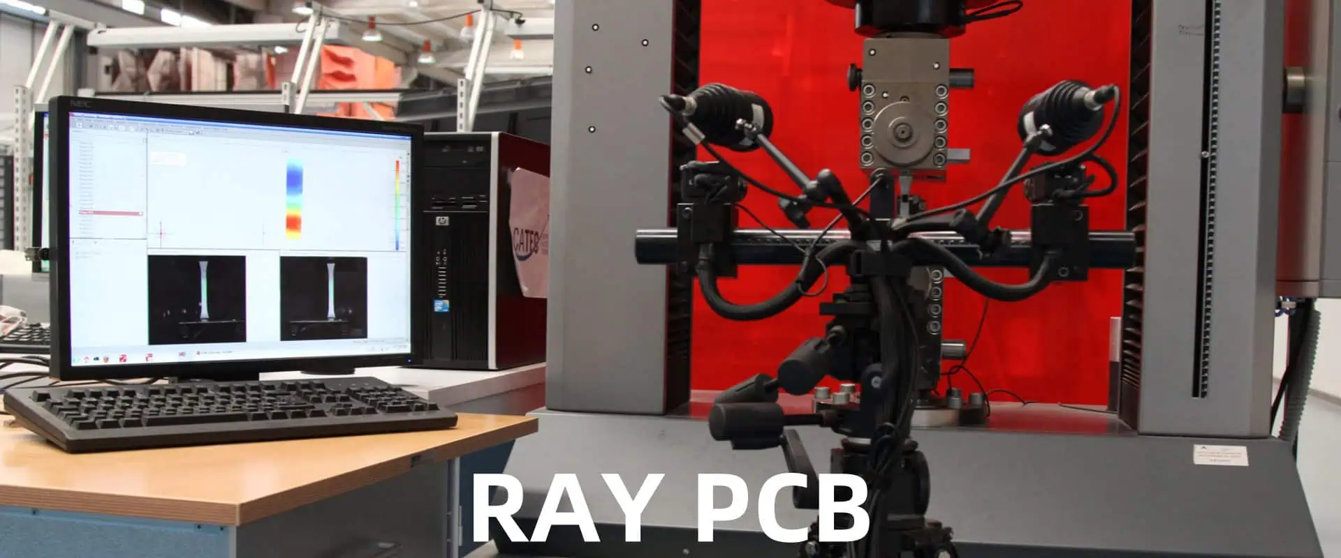
In the ever-evolving world of electronics manufacturing, the transition to lead-free printed circuit board (PCB) production has become a necessity driven by environmental concerns and stringent regulations. However, this shift has introduced new challenges, particularly in the realm of solder joint reliability and product quality assurance. To address these challenges, the adoption of advanced techniques like Digital Image Correlation (DIC) has proven invaluable. DIC is a powerful non-contact optical measurement technique that enables precise analysis of deformations and strains in materials, making it an indispensable tool for lead-free PCB manufacturing.

This comprehensive article delves into six effective ways DIC benefits lead-free PCB manufacturing, highlighting its critical role in ensuring product quality, reliability, and compliance with industry standards.

1. Solder Joint Integrity Assessment

One of the primary applications of DIC in lead-free PCB manufacturing is the assessment of solder joint integrity. During the reflow process, lead-free solder alloys can experience higher degrees of strain and deformation compared to their lead-based counterparts. DIC allows for detailed analysis of solder joint behavior under thermal cycling conditions, enabling manufacturers to identify potential issues and optimize their processes accordingly.

By precisely mapping the strain distributions within solder joints, DIC provides valuable insights into the quality and reliability of these critical interconnections. This information is crucial for validating the performance of lead-free solder alloys, ensuring long-term reliability, and minimizing the risk of premature failures.

2. Warpage Characterization and Mitigation

Warpage, or the deformation of PCBs during the manufacturing process, is a significant challenge in lead-free PCB production. The higher reflow temperatures required for lead-free soldering can exacerbate warpage issues, leading to potential reliability concerns and assembly challenges.

DIC offers a powerful solution for warpage characterization and mitigation. By accurately measuring the full-field deformations of PCBs during various stages of the manufacturing process, DIC enables manufacturers to identify the root causes of warpage and implement targeted countermeasures. This includes optimizing material selection, adjusting process parameters, and implementing specialized tooling or fixturing solutions.

3. Package-on-Package (PoP) Reliability Evaluation

In the realm of advanced packaging technologies, Package-on-Package (PoP) designs have gained significant traction due to their compact form factor and high functionality. However, the reliability of these complex structures remains a critical concern, particularly in lead-free PCB manufacturing environments.

DIC plays a crucial role in evaluating the reliability of PoP assemblies by enabling precise strain mapping and deformation analysis of the package-to-package interconnections. This information is invaluable for assessing the impact of thermal cycling, mechanical loading, and other environmental factors on the integrity of these interconnections, ultimately contributing to improved product reliability and quality.

4. Process Optimization and Design Validation

DIC’s ability to provide comprehensive deformation data across various materials and components makes it an invaluable tool for process optimization and design validation in lead-free PCB manufacturing.

By analyzing the strain distributions and deformations within PCBs, components, and interconnections during simulated manufacturing conditions, DIC allows for the validation of design choices and the optimization of process parameters. This includes assessing the impact of different material combinations, solder alloy compositions, and reflow profiles on the overall integrity and reliability of the final product.

5. Failure Analysis and Root Cause Identification

In the event of product failures or quality issues, DIC can be invaluable for conducting thorough failure analysis and identifying root causes. By analyzing the strain distributions and deformations within failed components or assemblies, DIC can provide insights into the underlying mechanisms that led to the failure.

This information is critical for implementing corrective actions, refining manufacturing processes, and preventing future occurrences of similar issues. DIC’s ability to pinpoint areas of localized strain or deformation can help identify potential weak points or design flaws, enabling targeted improvements and enhancing overall product quality and reliability.

6. Compliance with Industry Standards and Regulations

As lead-free PCB manufacturing becomes increasingly prevalent, adherence to industry standards and regulations is paramount. DIC plays a crucial role in ensuring compliance by providing quantitative data and objective evidence of product performance and reliability.

Many industry standards and guidelines, such as those established by organizations like IPC (Association Connecting Electronics Industries), require rigorous testing and validation of solder joint reliability, warpage control, and material compatibility. DIC’s precise measurement capabilities enable manufacturers to meet these requirements, demonstrating compliance and minimizing the risk of non-conformance issues.

BenefitDescription
Solder Joint Integrity AssessmentAnalyze solder joint behavior and strain distributions for quality and reliability assurance.
Warpage Characterization and MitigationMeasure full-field deformations to identify and mitigate warpage issues.
Package-on-Package (PoP) Reliability EvaluationAssess strain and deformations in PoP interconnections for reliability evaluation.
Process Optimization and Design ValidationValidate design choices and optimize process parameters based on deformation data.
Failure Analysis and Root Cause IdentificationPinpoint areas of localized strain or deformation for failure analysis and root cause identification.
Compliance with Industry Standards and RegulationsProvide quantitative data and evidence of product performance for compliance purposes.

FAQs

  1. Q: How does DIC compare to traditional strain measurement techniques in lead-free PCB manufacturing?ย A: Traditional strain measurement techniques, such as strain gauges or extensometers, are limited in their ability to measure localized strains or deformations across complex geometries. DIC, on the other hand, offers full-field, non-contact strain mapping capabilities, providing a more comprehensive understanding of deformation behavior across entire components or assemblies.
  2. Q: Is DIC suitable for real-time monitoring of manufacturing processes?ย A: While DIC can be used for real-time monitoring in certain applications, its primary strength in lead-free PCB manufacturing lies in offline analysis and validation. DIC systems capture high-resolution images during simulated manufacturing conditions or thermal cycling, which are then processed and analyzed to extract deformation data.
  3. Q: How does DIC contribute to the reliability evaluation of Package-on-Package (PoP) assemblies?ย A: DIC enables precise strain mapping and deformation analysis of the package-to-package interconnections in PoP assemblies. By quantifying the strains and deformations experienced by these interconnections under various environmental conditions, DIC provides valuable insights into their reliability and potential failure modes, enabling targeted improvements and design optimizations.
  4. Q: Can DIC be used for failure analysis in lead-free PCB manufacturing?ย A: Yes, DIC is an invaluable tool for failure analysis in lead-free PCB manufacturing. By analyzing the strain distributions and deformations within failed components or assemblies, DIC can help identify areas of localized strain or deformation, providing insights into the underlying mechanisms that led to the failure. This information is critical for implementing corrective actions and preventing future occurrences of similar issues.
  5. Q: How does DIC contribute to compliance with industry standards and regulations in lead-free PCB manufacturing?ย A: Many industry standards and guidelines, such as those established by organizations like IPC, require rigorous testing and validation of solder joint reliability, warpage control, and material compatibility. DIC’s precise measurement capabilities enable manufacturers to generate quantitative data and objective evidence of product performance and reliability, demonstrating compliance and minimizing the risk of non-conformance issues.

10 Benefits of Choosing Dedicated PCB Assembly Partner in USA

In today’s highly competitive and fast-paced electronics industry, having a reliable and efficient printed circuit board (PCB) assembly partner is crucial for success. As electronic devices become increasingly complex and compact, the demand for high-quality PCB assemblies has skyrocketed. Choosing a dedicated PCB assembly partner in the USA can offer numerous advantages, ranging from improved product quality and faster time-to-market to cost savings and better supply chain management.

This comprehensive article will explore the top 10 benefits of partnering with a dedicated PCB assembly company based in the United States, highlighting the key factors that make it a strategic choice for businesses of all sizes.

1. Proximity and Faster Lead Times

One of the primary advantages of working with a dedicated PCB assembly partner in the USA is the proximity factor. Having a local partner can significantly reduce lead times, enabling faster product development and quicker delivery to market. By eliminating the need for long-distance shipping and minimizing potential logistical delays, you can respond more effectively to market demands and stay ahead of the competition.

2. Stringent Quality Standards

The United States is known for its stringent quality standards and regulations in the electronics industry. Partnering with a dedicated PCB assembly company in the USA ensures that your products are manufactured in compliance with the highest quality and safety standards, such as IPC standards, RoHS, and UL certifications. This commitment to quality not only enhances product reliability and performance but also minimizes the risk of recalls and potential legal liabilities.

3. Access to Advanced Technologies and Expertise

The USA is a hub for cutting-edge technologies and innovation in the electronics industry. By partnering with a dedicated PCB assembly partner in the USA, you gain access to state-of-the-art equipment, advanced manufacturing processes, and a highly skilled workforce. These companies often invest heavily in research and development, ensuring that they stay at the forefront of technological advancements and can offer solutions that meet the most demanding requirements.

4. Intellectual Property Protection

Intellectual property (IP) protection is a critical concern for many businesses, particularly in the electronics industry. By choosing a dedicated PCB assembly partner in the USA, you can have greater confidence in the protection of your proprietary designs, trade secrets, and confidential information. The USA has robust intellectual property laws and enforcement mechanisms, providing an additional layer of security for your valuable assets.

5. Improved Supply Chain Management

Partnering with a local PCB assembly company can streamline your supply chain management processes. With shorter distances and better communication channels, you can more effectively collaborate with your partner, ensuring timely delivery of materials and components. This streamlined supply chain management can minimize disruptions, reduce inventory costs, and improve overall efficiency.

6. Customization and Flexibility

Dedicated PCB assembly partners in the USA often offer a high degree of customization and flexibility to meet the unique requirements of their clients. These companies have the expertise and resources to handle complex designs, special materials, and specific manufacturing processes. Whether you require small-batch production or large-scale manufacturing, a dedicated partner can tailor their services to your specific needs.

7. Regulatory Compliance Support

Navigating the complex regulatory landscape in the electronics industry can be a daunting task. By partnering with a dedicated PCB assembly company in the USA, you can benefit from their in-depth knowledge and expertise in complying with various regulations and standards. These companies stay up-to-date with the latest industry guidelines and can provide valuable guidance to ensure your products meet all necessary requirements.

8. Improved Communication and Collaboration

Working with a dedicated PCB assembly partner in the USA facilitates better communication and collaboration. With fewer language barriers and cultural differences, you can more effectively convey your requirements, discuss design changes, and address any issues that may arise during the manufacturing process. This improved communication leads to better understanding, faster problem-solving, and ultimately, a smoother overall experience.

9. Responsiveness and Customer Support

Dedicated PCB assembly partners in the USA typically prioritize responsiveness and customer support. With a local presence, you can benefit from more personalized attention and faster response times to your inquiries and concerns. Additionally, these companies often offer on-site support, technical assistance, and training, ensuring a seamless integration of their services into your operations.

10. Contribution to Local Economy and Job Creation

By partnering with a dedicated PCB assembly company in the USA, you contribute to the local economy and support job creation within the country. This not only fosters economic growth but also helps maintain a skilled workforce and promotes technological advancement in the electronics industry.

BenefitDescription
Proximity and Faster Lead TimesReduced lead times and quicker delivery to market due to proximity.
Stringent Quality StandardsCompliance with highest quality and safety standards in the USA.
Access to Advanced Technologies and ExpertiseAccess to cutting-edge equipment, processes, and skilled workforce.
Intellectual Property ProtectionRobust IP laws and enforcement mechanisms in the USA.
Improved Supply Chain ManagementStreamlined supply chain processes and reduced disruptions.
Customization and FlexibilityAbility to handle complex designs and specific requirements.
Regulatory Compliance SupportGuidance and expertise in navigating industry regulations.
Improved Communication and CollaborationBetter understanding and problem-solving due to fewer cultural barriers.
Responsiveness and Customer SupportPersonalized attention and faster response times.
Contribution to Local Economy and Job CreationSupport for local economic growth and job opportunities.

FAQs

  1. Q: How can I ensure the intellectual property protection of my designs when working with a dedicated PCB assembly partner in the USA?ย A: Reputable PCB assembly companies in the USA have robust measures in place to protect intellectual property, such as non-disclosure agreements (NDAs), secure data handling protocols, and strict access control measures. Additionally, the strong intellectual property laws and enforcement mechanisms in the USA provide an additional layer of protection.
  2. Q: Can a dedicated PCB assembly partner in the USA handle high-volume production requirements?ย A: Yes, many dedicated PCB assembly partners in the USA have the capability and resources to handle large-scale, high-volume production runs. These companies often have state-of-the-art facilities, advanced equipment, and streamlined processes to meet the demands of high-volume manufacturing.
  3. Q: How do dedicated PCB assembly partners in the USA ensure compliance with industry regulations and standards?ย A: Dedicated PCB assembly companies in the USA employ teams of experts who specialize in regulatory compliance. These experts stay up-to-date with the latest industry guidelines, standards, and regulations, such as IPC standards, RoHS, and UL certifications. They provide guidance and implement processes to ensure that all products meet the necessary requirements.
  4. Q: Can a dedicated PCB assembly partner in the USA offer customized solutions for my specific needs?ย A: Yes, one of the key advantages of partnering with a dedicated PCB assembly company in the USA is their ability to offer customized solutions. These companies have the expertise and resources to handle complex designs, special materials, and specific manufacturing processes. They work closely with clients to understand their unique requirements and tailor their services accordingly.
  5. Q: How can a dedicated PCB assembly partner in the USA contribute to improved supply chain management?ย A: By partnering with a local PCB assembly company, you can streamline your supply chain processes. Shorter distances and better communication channels enable more effective collaboration, timely delivery of materials and components, and reduced inventory costs. Additionally, a dedicated partner can help minimize disruptions and improve overall supply chain efficiency.

How Boundary-Scan Testing is Beneficial for PCB Assembly

Introduction

In the realm of printed circuit board (PCB) assembly, quality assurance and fault detection are paramount concerns. As electronic systems become increasingly complex and densely integrated, traditional testing methods often fall short in providing comprehensive coverage and accessibility. This is where boundary-scan testing emerges as a powerful solution, offering numerous benefits that streamline the manufacturing process, enhance quality control, and ultimately improve the overall reliability of electronic products.

Boundary-scan testing, also known as JTAG (Joint Test Action Group) testing, is a standardized methodology that utilizes specialized hardware and software to test interconnections, components, and functionality on PCBs. This article delves into the advantages of boundary-scan testing and how it can significantly enhance the PCB assembly process.

Understanding Boundary-Scan Testing

Boundary-scan testing is based on the IEEE 1149.1 standard, which defines a set of rules and protocols for testing interconnections and components on PCBs. The core concept revolves around incorporating specialized test logic, known as boundary-scan cells, into integrated circuits (ICs) during their design phase.

These boundary-scan cells act as controllable input/output points, allowing for the testing of interconnections between ICs and other components on the PCB. By leveraging these dedicated test points, boundary-scan testing can access and control individual pins or nodes on the PCB, enabling comprehensive testing and fault isolation capabilities.

Benefits of Boundary-Scan Testing for PCB Assembly

Boundary-scan testing offers numerous advantages that make it an invaluable tool for PCB assembly and quality assurance processes. Here are some of the key benefits:

1. Improved Test Coverage and Accessibility

Traditional testing methods, such as bed-of-nails fixtures or flying probe testers, often struggle to access dense and complex PCB designs with buried or inaccessible nodes. Boundary-scan testing overcomes this limitation by utilizing the dedicated test logic built into the ICs themselves, providing access to virtually every node on the PCB, including those that are physically inaccessible or buried beneath components.

2. Enhanced Fault Detection and Diagnostics

Boundary-scan testing allows for precise fault detection and diagnostics at the interconnection level. By controlling and monitoring individual pins and nodes, boundary-scan testing can identify open circuits, short circuits, and other interconnection-related defects with high accuracy. This level of granularity in fault detection enables more efficient root cause analysis and targeted repair or rework efforts.

3. Reduced Manufacturing Costs

By incorporating boundary-scan testing into the PCB assembly process, manufacturers can significantly reduce overall manufacturing costs. Improved test coverage and fault detection capabilities lead to fewer defective products reaching the end-user, reducing the need for costly field repairs or replacements. Additionally, boundary-scan testing can help streamline the manufacturing process by eliminating the need for complex and expensive test fixtures or probing systems.

4. Improved Product Quality and Reliability

Boundary-scan testing plays a crucial role in ensuring product quality and reliability. By thoroughly testing interconnections and components during the manufacturing process, potential defects or issues can be identified and addressed before the product reaches the customer. This proactive approach to quality assurance helps to minimize the risk of field failures and enhances overall product reliability.

5. Faster Time-to-Market

The efficiency and effectiveness of boundary-scan testing can contribute to faster time-to-market for new products. By streamlining the testing and debugging processes, manufacturers can shorten the overall development and production cycles, enabling them to bring their products to market more quickly while maintaining high quality standards.

6. Compliance with Industry Standards and Regulations

Many industries, such as aerospace, automotive, and medical electronics, have strict quality and safety regulations in place. Boundary-scan testing can help manufacturers comply with these standards by providing comprehensive testing and documentation capabilities. The IEEE 1149.1 standard itself is widely recognized and accepted across various industries, further reinforcing the credibility and compliance of boundary-scan testing.

Implementing Boundary-Scan Testing

To effectively implement boundary-scan testing in the PCB assembly process, manufacturers should consider the following steps:

  1. IC Selection: Choose ICs that support boundary-scan testing and comply with the IEEE 1149.1 standard. Many modern ICs, particularly those used in complex designs, are equipped with boundary-scan capabilities.
  2. Test Development: Develop comprehensive test programs and procedures specific to the PCB design. This may involve leveraging boundary-scan test development tools and creating test patterns tailored to the interconnections and components on the PCB.
  3. Test Integration: Integrate boundary-scan testing into the overall manufacturing and quality assurance processes. This may involve incorporating dedicated boundary-scan test equipment or integrating boundary-scan testing with existing test platforms.
  4. Training and Expertise: Ensure that appropriate training and expertise are available within the manufacturing team. Boundary-scan testing requires specialized knowledge and skills to effectively develop, execute, and interpret test results.
  5. Continuous Improvement: Continuously monitor and optimize the boundary-scan testing process. Regularly review test coverage, fault detection rates, and overall effectiveness to identify areas for improvement and adapt to evolving product designs and manufacturing requirements.

Data Visualization

To better illustrate the benefits of boundary-scan testing, let’s consider the following tables:

Table 1: Test Coverage Comparison

Testing MethodTest Coverage
Bed-of-Nails60-80%
Flying Probe70-90%
Boundary-Scan95-99%

This table compares the test coverage achieved by different testing methods. Boundary-scan testing offers significantly higher test coverage, ranging from 95% to 99%, compared to traditional methods like bed-of-nails or flying probe testers, which typically achieve lower coverage rates.

Table 2: Defect Detection and Yield Improvement

Testing MethodDefect Detection RateYield Improvement
No Testing
Traditional Methods60-80%10-20%
Boundary-Scan90-98%25-35%

This table illustrates the impact of different testing methods on defect detection rates and yield improvement. Boundary-scan testing can achieve defect detection rates of 90-98%, significantly higher than traditional methods. Consequently, boundary-scan testing can lead to yield improvements of 25-35%, resulting in substantial cost savings and improved product quality.

Table 3: Cost Savings with Boundary-Scan Testing

Cost FactorPotential Savings
Reduced Test Fixtures10-20%
Reduced Field Returns/Repairs15-25%
Increased Manufacturing Yield5-15%
Streamlined Debug and Rework10-20%

This table outlines the potential cost savings associated with implementing boundary-scan testing in the PCB assembly process. By reducing the need for expensive test fixtures, minimizing field returns and repairs, increasing manufacturing yield, and streamlining debug and rework processes, boundary-scan testing can contribute to significant cost savings across various areas of the manufacturing lifecycle.

These tables provide a visual representation of the advantages of boundary-scan testing, highlighting its superior test coverage, improved defect detection capabilities, and potential cost savings compared to traditional testing methods.

Frequently Asked Questions (FAQs)

  1. What is the difference between boundary-scan testing and traditional testing methods?ย Traditional testing methods, such as bed-of-nails fixtures or flying probe testers, access and test PCBs from the outside, often facing limitations in reaching buried or inaccessible nodes. In contrast, boundary-scan testing utilizes dedicated test logic built into the ICs themselves, allowing for comprehensive testing of interconnections and components, including those that are physically inaccessible.
  2. How does boundary-scan testing improve fault detection and diagnostics?ย Boundary-scan testing enables precise fault detection and diagnostics at the interconnection level. By controlling and monitoring individual pins and nodes, boundary-scan testing can identify open circuits, short circuits, and other interconnection-related defects with high accuracy. This level of granularity in fault detection facilitates more efficient root cause analysis and targeted repair or rework efforts.
  3. What are the benefits of boundary-scan testing in terms of cost savings?ย Boundary-scan testing can contribute to significant cost savings in various areas of the manufacturing process. It reduces the need for expensive test fixtures, minimizes field returns and repairs, increases manufacturing yield, and streamlines debug and rework processes. These cost savings can range from 10-25% across different cost factors.
  4. How does boundary-scan testing improve product quality and reliability?ย By thoroughly testing interconnections and components during the manufacturing process, boundary-scan testing helps identify and address potential defects or issues before the product reaches the customer. This proactive approach to quality assurance minimizes the

Best Practices of New Product Introduction (NPI) Manufacturing for Electronics Contract Manufacturers

In the ever-evolving world of electronics manufacturing, the ability to efficiently introduce new products to the market is a key competitive advantage for contract manufacturers. The New Product Introduction (NPI) process encompasses the crucial stages of transforming a product design into a scalable and cost-effective manufacturing reality. Effective NPI practices not only ensure a smooth transition from concept to production but also contribute to reduced time-to-market, improved product quality, and enhanced customer satisfaction.

This comprehensive guide aims to provide electronics contract manufacturers with a thorough understanding of the best practices for successful NPI manufacturing. By adopting these strategies, contract manufacturers can streamline their operations, minimize risks, and deliver high-quality products to their customers within the desired timelines.

Understanding the NPI Process

The NPI process is a multi-faceted endeavor that involves various stages and stakeholders. It typically encompasses the following phases:

1. Design Review and Validation

In this initial stage, the contract manufacturer thoroughly evaluates the product design, including schematics, bill of materials (BOM), and other relevant documentation. This review ensures that the design meets the specifications, identifies potential issues or design flaws, and validates the overall manufacturability of the product.

2. Supply Chain Management

Effective supply chain management is crucial for the successful execution of the NPI process. This stage involves identifying and qualifying suppliers, negotiating pricing and lead times, and establishing robust supply chain processes to ensure the timely availability of components and materials.

3. Manufacturing Process Development

During this phase, the contract manufacturer develops and optimizes the manufacturing processes tailored to the specific product requirements. This may include creating prototypes board, conducting design for manufacturability (DFM) analysis, establishing test procedures, and identifying potential production bottlenecks or quality control challenges.

4. Pilot Production and Validation

Once the manufacturing processes have been developed, the contract manufacturer initiates pilot production runs to validate the processes and identify any potential issues or areas for improvement. This stage also involves rigorous testing and quality assurance to ensure that the product meets all specifications and regulatory requirements.

5. Production Ramp-up and Monitoring

After successful pilot production, the contract manufacturer transitions to full-scale production. During this phase, continuous monitoring and process optimization are essential to maintain product quality, ensure efficient production flows, and meet customer demand.

Best Practices for NPI Manufacturing

Successful NPI manufacturing requires a strategic approach and adherence to industry best practices. Here are some key recommendations for electronics contract manufacturers:

1. Establish Clear Communication Channels

Effective communication is vital throughout the NPI process. Contract manufacturers should establish clear communication channels with customers, suppliers, and internal stakeholders. Regular meetings, progress reports, and documented procedures can help ensure that all parties are aligned and potential issues are addressed promptly.

2. Implement Design for Manufacturability (DFM) Principles

Incorporating DFM principles early in the design phase can significantly streamline the manufacturing process and reduce costs. DFM analysis involves evaluating the product design for ease of assembly, testability, and manufacturability, identifying potential issues, and suggesting design optimizations to improve overall efficiency.

3. Leverage Advanced Manufacturing Technologies

Adopting advanced manufacturing technologies, such as automated assembly lines, smart sensors, and data analytics, can greatly enhance the NPI process. These technologies enable efficient production, real-time monitoring, and data-driven decision-making, ultimately leading to improved quality, reduced waste, and increased productivity.

4. Conduct Thorough Supply Chain Risk Assessment

A comprehensive supply chain risk assessment is crucial for mitigating potential disruptions and ensuring a stable flow of components and materials. Contract manufacturers should evaluate suppliers based on criteria such as quality, reliability, financial stability, and geographic location, and develop contingency plans to address potential supply chain challenges.

5. Implement Robust Quality Control Measures

Rigorous quality control measures are essential throughout the NPI process, from design review to production ramp-up. Contract manufacturers should establish comprehensive testing procedures, implement statistical process control (SPC) techniques, and invest in advanced inspection and testing equipment to ensure product quality and compliance with industry standards and regulations.

6. Foster Cross-Functional Collaboration

NPI manufacturing involves various functional areas, including engineering, procurement, production, quality control, and logistics. Fostering cross-functional collaboration and breaking down silos can enhance communication, facilitate problem-solving, and promote a holistic approach to the NPI process.

7. Continuously Improve and Optimize Processes

The NPI process should be viewed as a continuous improvement journey. Contract manufacturers should regularly analyze performance data, identify areas for optimization, and implement process improvements. This proactive approach can lead to increased efficiency, reduced costs, and improved customer satisfaction.

Data Visualization

To better illustrate the impact of effective NPI practices, let’s consider the following tables:

Table 1: NPI Lead Time Reduction

NPI Practice Lead Time Reduction
Design for Manufacturability (DFM) 20-30%
Supply Chain Risk Assessment 10-15%
Advanced Manufacturing Technologies 15-25%
Cross-Functional Collaboration 10-20%

This table demonstrates the potential lead time reductions that can be achieved by implementing various NPI best practices. For example, incorporating DFM principles can reduce lead times by 20-30%, while fostering cross-functional collaboration can lead to a 10-20% reduction in lead times.

Table 2: Impact of NPI Practices on Product Quality

NPI Practice Quality Improvement
Robust Quality Control Measures 30-40%
Advanced Inspection and Testing Equipment 20-30%
Statistical Process Control (SPC) 15-25%
Continuous Process Improvement 10-20%

This table illustrates how various NPI practices can positively impact product quality. Implementing robust quality control measures, such as advanced inspection and testing equipment and SPC techniques, can lead to substantial improvements in product quality, ranging from 20-40%.

Table 3: NPI Cost Savings

NPI Practice Cost Savings
Design Optimizations 10-20%
Supply Chain Management 5-15%
Process Optimization 8-15%
Reduced Rework and Waste 5-10%

Effective NPI practices can also lead to significant cost savings for contract manufacturers. This table highlights potential cost savings achieved through design optimizations, supply chain management, process optimization, and reduced rework and waste, ranging from 5-20% depending on the specific practice implemented.

These tables provide a visual representation of the quantitative impact that NPI best practices can have on various aspects of the manufacturing process, including lead times, product quality, and cost savings. By adopting these practices, contract manufacturers can gain a competitive edge and deliver exceptional value to their customers.

Frequently Asked Questions (FAQs)

  1. What is the significance of the NPI process for electronics contract manufacturers?ย The NPI process is crucial for electronics contract manufacturers as it enables them to efficiently transition from product design to scalable and cost-effective manufacturing. Effective NPI practices contribute to reduced time-to-market, improved product quality, and enhanced customer satisfaction, ultimately providing a competitive advantage in the market.
  2. How can contract manufacturers ensure effective communication during the NPI process?ย To ensure effective communication, contract manufacturers should establish clear communication channels with customers, suppliers, and internal stakeholders. Regular meetings, progress reports, and documented procedures can help maintain alignment and promptly address potential issues. Additionally, fostering cross-functional collaboration and breaking down silos can enhance communication and facilitate problem-solving.
  3. What is the role of Design for Manufacturability (DFM) in the NPI process?ย DFM plays a crucial role in streamlining the NPI process and reducing costs. It involves evaluating the product design for ease of assembly, testability, and manufacturability, and suggesting design optimizations to improve overall efficiency. Incorporating DFM principles early in the design phase can significantly contribute to lead time reductions and cost savings.
  4. How can contract manufacturers mitigate supply chain risks during the NPI process?ย To mitigate supply chain risks, contract manufacturers should conduct a comprehensive supply chain risk assessment. This involves evaluating suppliers based on criteria such as quality, reliability, financial stability, and geographic location. Additionally, developing contingency plans and implementing robust supply chain management practices can help address potential disruptions and ensure a stable flow of components and materials.
  5. What are the benefits of adopting advanced manufacturing technologies in the NPI process?ย Adopting advanced manufacturing technologies, such as automated assembly lines, smart sensors, and data analytics, can greatly enhance the NPI process. These technologies enable efficient production, real-time monitoring, and data-driven decision-making, ultimately leading to improved quality, reduced waste, and increased productivity. Furthermore, they can contribute to lead time reductions and cost savings through process optimization and increased efficiency.

Complete Guide on Copper Balance in Printed Circuit Board Fabrication

Copper balance is a critical aspect of printed circuit board (PCB) fabrication that directly impacts the quality, performance, and reliability of the final product. It refers to the precise control and management of copper distribution throughout the manufacturing process, ensuring that the desired copper thickness and patterns are achieved on the PCB layers.

In this comprehensive guide, we will delve into the intricacies of copper balance, exploring its significance, the factors that influence it, and the techniques employed to maintain optimal copper distribution during PCB fabrication.

Understanding Copper Balance

Copper balance is essential for several reasons:

  1. Signal Integrity: Consistent copper thickness and uniformity across the PCB help maintain signal integrity, minimizing signal distortion, crosstalk, and electromagnetic interference (EMI).
  2. Thermal Management: Proper copper balance ensures efficient heat dissipation, preventing hot spots and minimizing thermal stress on components.
  3. Reliability: Uneven copper distribution can lead to stress concentrations, increasing the risk of cracks, delamination, and other defects, ultimately compromising the PCB’s reliability.
  4. Manufacturing Yield: Achieving copper balance reduces the likelihood of defects, improving manufacturing yield and reducing waste.

Factors Influencing Copper Balance

Several factors can affect copper balance during PCB fabrication, including:

1. Copper Plating Process

The copper plating process is the primary determinant of copper distribution on the PCB. Factors such as plating bath composition, current density, and plating time can significantly impact the uniformity and thickness of the deposited copper layer.

Plating Bath Composition

The plating bath composition, including the concentrations of copper ions, additives, and other chemicals, plays a crucial role in controlling the plating rate and uniformity. Imbalances in the bath composition can lead to uneven copper distribution or defective plating.

Current Density

The current density during the plating process determines the rate of copper deposition. Maintaining a uniform current density across the entire surface area of the PCB is essential for achieving consistent copper thickness.

Plating Time

The plating time, or the duration of the plating process, directly affects the overall copper thickness. Accurate control of plating time is necessary to achieve the desired copper thickness while minimizing over-plating or under-plating.

2. Panel Design and Layout

The design and layout of the PCB panel can significantly influence copper balance. Factors such as trace patterns, copper area distribution, and panel panelization can impact the uniformity of copper deposition.

Trace Patterns

Complex trace patterns or high-density interconnects can create localized areas with higher or lower copper concentrations, leading to imbalances in copper distribution.

Copper Area Distribution

The distribution of copper areas (e.g., planes, pads, and traces) across the PCB panel affects the current density and plating rate, potentially causing variations in copper thickness.

Panel Panelization

The way PCB panels are arranged and subdivided (panelization) can influence the current distribution and plating uniformity, especially at the edges and corners of the panel.

3. Plating Equipment and Setup

The plating equipment and setup, including the anode configuration, fluid dynamics, and electrical field distribution, can significantly impact copper balance.

Anode Configuration

The placement, shape, and number of anodes in the plating tank influence the current distribution and plating uniformity across the PCB panel.

Fluid Dynamics

The flow patterns and turbulence of the plating solution can affect the mass transfer of copper ions and additives, leading to variations in plating rates and copper thickness.

Electrical Field Distribution

The distribution of the electrical field within the plating tank plays a crucial role in determining the current density and plating uniformity across the PCB panel.

Techniques for Maintaining Copper Balance

To achieve optimal copper balance during PCB fabrication, several techniques are employed:

1. Plating Process Optimization

Optimizing the plating process is crucial for maintaining copper balance. This involves:

  • Plating Bath Monitoring and Adjustment: Regular monitoring and adjustment of the plating bath composition, including the concentrations of copper ions, additives, and other chemicals, to ensure consistent plating rates and uniformity.
  • Current Density Control: Implementing advanced current control systems to maintain uniform current density across the entire PCB panel surface, accounting for variations in trace patterns and copper area distribution.
  • Plating Time Monitoring: Precise monitoring and control of plating time to achieve the desired copper thickness while minimizing over-plating or under-plating.

2. Panel Design Optimization

Optimizing the panel design and layout can significantly improve copper balance:

  • Copper Area Balancing: Strategically distributing copper areas (e.g., planes, pads, and traces) across the PCB panel to minimize current density variations and ensure uniform plating rates.
  • Panelization Optimization: Carefully considering the panel panelization strategy to minimize the impact of edge effects and ensure uniform current distribution across the entire panel.

3. Plating Equipment Enhancements

Advancements in plating equipment and setups can contribute to improved copper balance:

  • Anode Configuration Optimization: Employing specialized anode configurations, such as auxiliary anodes or shielding, to achieve more uniform current distribution and plating rates across the PCB panel.
  • Fluid Dynamics Optimization: Implementing advanced agitation systems or flow-controlled plating cells to optimize the mass transfer of copper ions and additives, ensuring consistent plating rates throughout the panel.
  • Electrical Field Shaping: Utilizing specialized electrical field shaping techniques, such as the use of thiefing shields or auxiliary electrodes, to shape the electrical field distribution and achieve uniform current density across the PCB panel.

4. In-Line Monitoring and Feedback Control

Implementing advanced in-line monitoring and feedback control systems can significantly enhance copper balance by allowing real-time adjustments and corrections during the plating process:

  • Thickness Monitoring: Employing in-line thickness monitoring systems, such as eddy current or optical sensors, to continuously measure copper thickness across the PCB panel.
  • Feedback Control Systems: Integrating feedback control systems that can automatically adjust plating parameters (e.g., current density, plating time, or bath composition) based on real-time thickness measurements, ensuring consistent copper distribution throughout the plating process.

Data Visualization

To better illustrate the importance of copper balance and the impact of various factors, let’s consider the following tables:

Table 1: Copper Thickness Variation across a PCB Panel

Panel RegionCopper Thickness (ฮผm)
Center35.2
Top-Left33.8
Top-Right34.5
Bottom-Left36.1
Bottom-Right35.7

In this example, the copper thickness varies across different regions of the PCB panel, with the center having the desired thickness of 35.2 ฮผm, while the edges and corners exhibit deviations ranging from 33.8 ฮผm to 36.1 ฮผm. Such variations can lead to inconsistencies in signal integrity, thermal management, and reliability across the PCB.

Table 2: Impact of Plating Time on Copper Thickness

Plating Time (minutes)Copper Thickness (ฮผm)
6032.5
6534.8
7037.2
7539.6

This table demonstrates the direct relationship between plating time and copper thickness. Deviations from the desired plating time can result in either under-plating or over-plating, leading to copper thickness variations that can compromise the PCB’s performance and reliability.

Table 3: Effect of Current Density on Copper Plating Rate

Current Density (A/dmยฒ)Plating Rate (ฮผm/min)
2.00.42
2.50.55
3.00.68
3.50.79

The current density during the plating process directly affects the plating rate, as illustrated in this table. Variations in current density across the PCB panel can lead to non-uniform copper deposition, potentially causing thickness variations and imbalances.

These tables provide visual representations of how different factors can influence copper balance during PCB fabrication, highlighting the importance of precise control and optimization to achieve consistent and reliable copper distribution.

Ensure your Power Distribution Network PCB Requirements with amazing tips!

Introduction to Power Distribution Network PCB Design

The power distribution network (PDN) is a critical component of any electronic system, responsible for delivering clean and stable power to the various subsystems and components. The design of the PDN PCB plays a crucial role in ensuring the overall performance, reliability, and efficiency of the electronic device. In this article, we will explore the key considerations and best practices for designing an effective power distribution network PCB that meets the unique requirements of your application.

Importance of Robust Power Distribution Network Design

The power distribution network is the foundation upon which the entire electronic system is built. Its design directly impacts the following aspects of the system:

  1. Reliability: A well-designed PDN ensures that the electronic components receive the necessary power without voltage drops or noise, preventing malfunctions and increasing system reliability.
  2. Performance: A stable and clean power supply enables the electronic components to operate at their optimal performance levels, enhancing the overall system capabilities.
  3. Efficiency: An efficient PDN design minimizes power losses, reducing energy consumption and improving the overall energy efficiency of the electronic device.
  4. Electromagnetic Compatibility (EMC): Proper PDN design helps mitigate electromagnetic interference (EMI) and ensures the system’s compliance with electromagnetic compatibility standards.

Key Considerations in Power Distribution Network PCB Design

Designing an effective power distribution network PCB requires a careful consideration of several factors, including:

1. Power Requirements

Accurately determining the power requirements of the electronic system is the foundation of PDN design. This includes understanding the voltage levels, current demands, and power consumption of each subsystem and component.

2. Voltage Regulation and Stability

Ensuring a stable and regulated power supply is crucial for the proper operation of electronic components. This involves the selection and placement of voltage regulators, decoupling capacitors, and other power management components.

3. Impedance Management

The impedance of the PDN, including the traces, planes, and vias, can significantly impact the power quality and signal integrity. Proper impedance management techniques, such as controlled impedance routing and optimal trace widths, are essential.

4. Thermal Management

The power dissipation in the PDN can generate significant heat, which must be effectively managed to prevent thermal-related issues and maintain the system’s reliability.

5. Electromagnetic Compatibility (EMC)

The PDN design must account for electromagnetic compatibility, minimizing the generation and propagation of electromagnetic interference (EMI) within the system and ensuring compliance with relevant standards.

6. Reliability and Robustness

The PDN design must ensure the long-term reliability and robustness of the electronic system, considering factors such as environmental conditions, vibration, and potential failure modes.

Best Practices for Power Distribution Network PCB Design

To ensure the optimal performance and reliability of your power distribution network PCB, consider the following best practices:

1. Accurate Power Requirements Analysis

Conduct a thorough analysis of the power requirements for each subsystem and component, considering the peak and average power consumption, voltage levels, and current demands. This information will guide the selection of the appropriate power supply and regulation components.

2. Hierarchical Power Distribution

Implement a hierarchical power distribution approach, where the main power supply is divided into multiple voltage domains, each with its own regulation and filtering. This helps isolate different sections of the circuit and improves overall power quality.

3. Optimized Plane and Trace Design

Carefully design the power and ground planes to ensure low-impedance connections and minimize the risk of voltage drops and noise. Optimize the trace widths and lengths to manage the impedance and power distribution.

4. Comprehensive Decoupling Strategy

Implement a robust decoupling strategy, utilizing high-frequency and low-frequency decoupling capacitors at strategic locations throughout the PCB. This helps to maintain a stable power supply and mitigate the effects of transient events.

5. Thermal Management Techniques

Incorporate effective thermal management techniques, such as the use of heat sinks, thermal vias, and airflow considerations, to ensure the reliable operation of the power distribution network under various load conditions.

6. Electromagnetic Compatibility (EMC) Design

Adhere to EMC design principles, including the use of appropriate trace routing, grounding strategies, and shielding techniques, to minimize the generation and propagation of electromagnetic interference within the system.

7. Reliability and Robustness Assessment

Assess the long-term reliability and robustness of the power distribution network PCB design, considering factors such as environmental conditions, vibration, and potential failure modes. Implement appropriate design measures to ensure the system’s durability and longevity.

Tables for Visualization

To further illustrate the key considerations and best practices for power distribution network PCB design, we have provided the following tables:

Table 1: Key Considerations in Power Distribution Network PCB Design

ConsiderationDescription
Power RequirementsAccurately determining voltage levels, current demands, and power consumption of each subsystem and component.
Voltage Regulation and StabilityEnsuring a stable and regulated power supply through the selection and placement of voltage regulators and decoupling capacitors.
Impedance ManagementControlling the impedance of traces, planes, and vias to maintain power quality and signal integrity.
Thermal ManagementImplementing effective heat dissipation techniques to prevent thermal-related issues.
Electromagnetic Compatibility (EMC)Designing the PDN to minimize electromagnetic interference and ensure compliance with relevant standards.
Reliability and RobustnessEnsuring the long-term reliability and durability of the PDN under various environmental and operating conditions.

Table 2: Best Practices for Power Distribution Network PCB Design

Best PracticeDescription
Accurate Power Requirements AnalysisConducting a thorough analysis of the power requirements for each subsystem and component.
Hierarchical Power DistributionImplementing a hierarchical power distribution approach to isolate different sections of the circuit.
Optimized Plane and Trace DesignCarefully designing power and ground planes and optimizing trace widths and lengths.
Comprehensive Decoupling StrategyImplementing a robust decoupling strategy with high-frequency and low-frequency capacitors.
Thermal Management TechniquesIncorporating effective thermal management techniques, such as heat sinks and thermal vias.
Electromagnetic Compatibility (EMC) DesignAdhering to EMC design principles, including appropriate trace routing and shielding.
Reliability and Robustness AssessmentAssessing the long-term reliability and robustness of the PDN design under various environmental and operating conditions.

FAQ (Frequently Asked Questions)

  1. Q: Why is the power distribution network PCB design crucial for the overall performance and reliability of an electronic system?ย A: The power distribution network PCB design is crucial because it directly impacts the reliability, performance, efficiency, and electromagnetic compatibility of the electronic system. A well-designed PDN ensures that the electronic components receive a stable and clean power supply, enabling them to operate at their optimal levels and preventing malfunctions or failures.
  2. Q: How does the hierarchical power distribution approach improve the power quality and reliability of the electronic system?ย A: The hierarchical power distribution approach involves dividing the main power supply into multiple voltage domains, each with its own regulation and filtering. This helps to isolate different sections of the circuit, preventing the propagation of noise and transients, and improving the overall power quality and reliability of the system.
  3. Q: What are the key considerations in managing the impedance of the power distribution network PCB?ย A: Proper impedance management in the PDN PCB design is crucial for maintaining power quality and signal integrity. Key considerations include controlling the impedance of traces, planes, and vias through optimized trace widths and lengths, as well as implementing appropriate decoupling strategies to manage the high-frequency and low-frequency impedances.
  4. Q: How do thermal management techniques contribute to the reliability and longevity of the power distribution network PCB?ย A: Effective thermal management techniques, such as the use of heat sinks, thermal vias, and airflow considerations, are essential for dissipating the heat generated in the PDN. This helps to prevent thermal-related issues, such as component degradation, and ensures the reliable and long-term operation of the electronic system.
  5. Q: What are the key electromagnetic compatibility (EMC) design principles that should be considered in the power distribution network PCB design?ย A: The key EMC design principles for the PDN PCB include appropriate trace routing, grounding strategies, and shielding techniques to minimize the generation and propagation of electromagnetic interference (EMI) within the system. This helps to ensure the system’s compliance with relevant EMC standards and prevents interference with other electronic components or systems.

Conclusion

Designing an effective power distribution network PCB is crucial for the overall performance, reliability, and efficiency of electronic systems. By considering the key factors, such as power requirements, voltage regulation, impedance management, thermal management, and electromagnetic compatibility, and implementing the best practices outlined in this article, you can ensure that your power distribution network PCB meets the unique requirements of your application. A well-designed PDN PCB will contribute to the long-term reliability and stability of your electronic device, providing a solid foundation for its optimal performance and seamless operation.

EV Charger PCB Assemblies enhance safety, efficiency, and reliability!

Introduction to EV Charger PCB Assemblies

The growing adoption of electric vehicles (EVs) has led to an increasing demand for reliable and efficient charging solutions. At the heart of these charging systems are the Printed Circuit Board (PCB) assemblies, which play a crucial role in ensuring the safety, efficiency, and reliability of EV chargers. In this article, we will explore the key aspects of EV charger PCB assemblies, highlighting the best practices and emerging trends that contribute to the enhanced performance of these critical components.

The Importance of EV Charger PCB Assemblies

EV charger PCB assemblies are responsible for managing the complex electrical processes involved in charging electric vehicles. These assemblies are designed to handle high-power electrical loads, sophisticated control systems, and advanced communication protocols. The proper design, manufacturing, and assembly of these PCBs are essential for the overall performance and safety of EV charging stations.

Enhancing Safety

Safety is a paramount concern in the design and implementation of EV charger PCB assemblies. These assemblies must comply with rigorous safety standards and regulations to protect both the charging station and the vehicle from potential hazards. Key safety features include:

  • Overcurrent and overvoltage protection
  • Thermal management systems
  • Grounding and insulation mechanisms
  • Fault detection and shutdown procedures

Improving Efficiency

EV charger PCB assemblies play a crucial role in ensuring the efficient transfer of energy from the power grid to the vehicle’s battery. Optimized PCB design, component selection, and control algorithms can significantly improve the energy efficiency of the charging process, reducing power losses and minimizing the environmental impact of EV charging.

Ensuring Reliability

The reliability of EV charger PCB assemblies is essential for providing a seamless and hassle-free charging experience for EV owners. These assemblies must be designed to withstand the rigors of continuous operation, environmental stresses, and potential electrical disturbances. Robust construction, component selection, and testing procedures contribute to the long-term reliability of EV charger PCB assemblies.

Key Design Considerations for EV Charger PCB Assemblies

Designing effective EV charger PCB assemblies requires careful consideration of various factors, including:

1. Power Handling Capabilities

EV charger PCB assemblies must be capable of handling the high-power electrical loads required for charging EVs. This involves optimizing the PCB layout, trace widths, and component selection to ensure the safe and efficient transfer of power.

2. Thermal Management

The high-power operation of EV charger PCB assemblies generates significant heat, which must be effectively dissipated to maintain optimal performance and reliability. Thermal management strategies, such as the use of heat sinks, cooling fans, and thermal vias, are crucial design considerations.

3. Electromagnetic Compatibility (EMC)

EV charger PCB assemblies operate in an environment with various electromagnetic sources, both from the power grid and the vehicle itself. Careful design of the PCB layout, component selection, and shielding techniques are necessary to ensure electromagnetic compatibility and minimize interference.

4. Control and Communication Protocols

EV charger PCB assemblies must integrate advanced control systems and communication protocols to manage the charging process, monitor the system status, and enable remote monitoring and control. This involves the implementation of microcontrollers, communication interfaces, and firmware programming.

5. Cybersecurity and Data Protection

As EV charger PCB assemblies become increasingly connected to the internet and cloud-based services, the need for robust cybersecurity measures and data protection mechanisms becomes crucial. Secure communication protocols, access control, and data encryption are essential design considerations.

6. Mechanical and Environmental Considerations

EV charger PCB assemblies must be designed to withstand the environmental conditions in which they operate, such as temperature extremes, humidity, vibration, and weathering. The mechanical design, enclosure, and material selection are crucial factors in ensuring the long-term reliability of these assemblies.

Best Practices for EV Charger PCB Assembly

To ensure the optimal performance and reliability of EV charger PCB assemblies, the following best practices should be implemented:

1. Component Selection and Sourcing

Careful selection of high-quality, reliable components is essential for the overall performance and longevity of EV charger PCB assemblies. This includes power semiconductors, capacitors, resistors, and other critical components.

2. Precise PCB Layout and Design

The PCB layout plays a crucial role in the efficient and safe operation of EV charger assemblies. Considerations such as trace width, component placement, and heat dissipation paths are crucial for optimal performance.

3. Advanced Assembly Techniques

Employing advanced assembly techniques, such as reflow soldering, selective soldering, and conformal coating, can improve the reliability and durability of EV charger PCB assemblies.

4. Rigorous Testing and Validation

Comprehensive testing and validation procedures, including functional testing, environmental stress testing, and reliability assessments, are essential for ensuring the safety and performance of EV charger PCB assemblies.

5. Traceability and Quality Control

Maintaining detailed traceability of components, assembly processes, and quality control measures is crucial for identifying and addressing any issues that may arise during the lifetime of the EV charger.

Tables for Visualization

To further illustrate the key design considerations and best practices for EV charger PCB assemblies, we have provided the following tables:

Table 1: Key Design Considerations for EV Charger PCB Assemblies

Design ConsiderationDescription
Power Handling CapabilitiesOptimizing PCB layout, trace widths, and component selection for high-power operation.
Thermal ManagementImplementing heat sinks, cooling fans, and thermal vias for effective heat dissipation.
Electromagnetic Compatibility (EMC)Ensuring PCB layout, component selection, and shielding techniques minimize electromagnetic interference.
Control and Communication ProtocolsIntegrating microcontrollers, communication interfaces, and firmware for advanced control and monitoring.
Cybersecurity and Data ProtectionImplementing secure communication protocols, access control, and data encryption mechanisms.
Mechanical and Environmental ConsiderationsDesigning for environmental conditions, including temperature, humidity, vibration, and weathering.

Table 2: Best Practices for EV Charger PCB Assembly

Best PracticeDescription
Component Selection and SourcingChoosing high-quality, reliable components for optimal performance and longevity.
Precise PCB Layout and DesignOptimizing trace width, component placement, and heat dissipation paths for efficient and safe operation.
Advanced Assembly TechniquesEmploying reflow soldering, selective soldering, and conformal coating to improve reliability and durability.
Rigorous Testing and ValidationConducting functional testing, environmental stress testing, and reliability assessments to ensure safety and performance.
Traceability and Quality ControlMaintaining detailed records of components, assembly processes, and quality control measures for effective issue identification and resolution.

FAQ (Frequently Asked Questions)

  1. Q: What are the key safety features of EV charger PCB assemblies?ย A: EV charger PCB assemblies incorporate several safety features, such as overcurrent and overvoltage protection, thermal management systems, grounding and insulation mechanisms, and fault detection and shutdown procedures. These features are designed to safeguard both the charging station and the vehicle during the charging process.
  2. Q: How do EV charger PCB assemblies contribute to the overall efficiency of the charging process?ย A: EV charger PCB assemblies play a crucial role in improving the energy efficiency of the charging process. Optimized PCB design, component selection, and control algorithms can minimize power losses and ensure the efficient transfer of energy from the power grid to the vehicle’s battery.
  3. Q: What are the key factors that contribute to the reliability of EV charger PCB assemblies?ย A: The reliability of EV charger PCB assemblies is ensured through robust construction, the selection of high-quality components, and rigorous testing procedures. Factors such as thermal management, environmental protection, and the implementation of advanced assembly techniques are critical for enhancing the long-term reliability of these assemblies.
  4. Q: How do cybersecurity and data protection considerations impact the design of EV charger PCB assemblies?ย A: As EV charger PCB assemblies become more connected to the internet and cloud-based services, the need for robust cybersecurity measures and data protection mechanisms is paramount. This includes the implementation of secure communication protocols, access control, and data encryption to safeguard the charging system and the user’s personal information.
  5. Q: What are the key environmental and mechanical considerations in the design of EV charger PCB assemblies?ย A: EV charger PCB assemblies must be designed to withstand the environmental conditions in which they operate, such as temperature extremes, humidity, vibration, and weathering. The mechanical design, enclosure, and material selection are crucial factors in ensuring the long-term reliability and durability of these assemblies.

Conclusion

EV charger PCB assemblies are the backbone of the rapidly evolving electric vehicle charging infrastructure. By prioritizing safety, efficiency, and reliability in the design and assembly of these critical components, manufacturers can contribute to the widespread adoption and acceptance of electric vehicles. Through the implementation of best practices, such as careful component selection, precise PCB layout, advanced assembly techniques, and rigorous testing and validation, EV charger PCB assemblies can deliver enhanced performance, improved user experience, and a more sustainable future for electric mobility.

Best Practices to Ensure the Correct Component Orientation by Optimized assembly PCB board!

Introduction to Component Orientation in PCB Assembly

Printed Circuit Board (PCB) assembly is a critical process in the manufacture of electronic devices, as it involves the placement and soldering of components onto the board. Ensuring the correct orientation of these components is crucial to the proper functioning and reliability of the final product. Incorrect component orientation can lead to a variety of issues, ranging from malfunctioning circuits to complete device failure. In this article, we will explore the best practices to ensure the correct component orientation during the PCB assembly process, with a focus on optimized assembly techniques.

Importance of Correct Component Orientation

The orientation of components on a PCB is essential for several reasons:

  1. Functionality: Components, such as integrated circuits, transistors, and diodes, are designed to function correctly only when placed in a specific orientation. Incorrect orientation can lead to the component not working as intended or even causing damage to the circuit.
  2. Electrical Connections: The placement and orientation of components on a PCB determine the electrical connections between them. Improper orientation can result in incorrect signal flow, leading to circuit malfunctions or even short circuits.
  3. Thermal Management: The orientation of components can impact the heat dissipation and overall thermal management of the PCB. Incorrect placement can cause hot spots or uneven heat distribution, affecting the device’s performance and reliability.
  4. Mechanical Stability: The orientation of components can also impact the mechanical stability of the PCB, particularly in high-vibration or high-shock environments. Improperly oriented components can become dislodged or damaged over time, leading to reliability issues.

Best Practices for Ensuring Correct Component Orientation

To ensure the correct orientation of components during PCB assembly, there are several best practices that can be implemented:

1. Comprehensive Component Documentation

Accurate and up-to-date documentation is the foundation for ensuring correct component orientation. This includes:

  • Component Datasheets: Carefully review the component datasheets to understand the correct orientation of pins, leads, and other critical features.
  • Assembly Drawings: Refer to the PCB assembly drawings or schematics to identify the correct orientation of each component on the board.
  • Component Orientation Markings: Utilize the orientation markings (e.g., pin 1 indicator, polarity marks) on the components and the PCB to verify the correct placement.

2. Optimized Stencil Design

The stencil design plays a crucial role in ensuring correct component orientation during the solder paste printing process. Consider the following best practices:

  • Stencil Aperture Alignment: Ensure that the stencil apertures are precisely aligned with the component pads on the PCB to prevent improper solder paste deposition.
  • Stencil Thickness: Adjust the stencil thickness to match the component height and ensure sufficient solder paste volume for reliable solder joints.
  • Stencil Aperture Geometry: Design the stencil apertures to match the component footprints and pad layouts, minimizing the risk of misalignment.

3. Automated Component Placement

Utilizing automated placement equipment, such as pick-and-place machines, can significantly improve the accuracy and consistency of component orientation during assembly. These machines are programmed with component orientation information and can precisely place components on the PCB based on the design specifications.

4. Visual Inspection and Verification

Implement a robust visual inspection process to ensure the correct orientation of components after the placement phase. This can include:

  • Component Orientation Checks: Visually inspect the placement of each component to verify that it matches the design specifications and orientation markings.
  • Solder Joint Inspection: Examine the solder joints to ensure that they are properly formed and that there are no signs of bridging or other defects that could indicate improper component orientation.
  • Sample Inspection: Regularly inspect a sample of assembled boards to identify and address any issues with component orientation.

5. Traceability and Documentation

Maintain thorough documentation and traceability throughout the PCB assembly process. This includes:

  • Assembly Process Records: Document the assembly process, including the placement of components, solder paste application, and any quality control checks.
  • Component Tracking: Establish a system to track the components used in each assembly, including their lot numbers and other relevant information.
  • Non-conformance Reporting: Establish a process for reporting and addressing any instances of incorrect component orientation or other assembly issues.

6. Continuous Improvement and Training

Continuously review and optimize the PCB assembly process to identify and address any recurring issues related to component orientation. This can include:

  • Operator Training: Provide comprehensive training to assembly operators on the importance of correct component orientation and the best practices for achieving it.
  • Process Monitoring and Analysis: Regularly analyze the assembly data and quality metrics to identify areas for improvement and implement corrective actions.
  • Supplier Collaboration: Work closely with component suppliers to ensure that the components are consistently delivered with accurate orientation markings and documentation.

Tables for Visualization

To further enhance the understanding of the best practices discussed in this article, we have provided the following tables:

Table 1: Checklist for Comprehensive Component Documentation

Documentation RequirementDescription
Component DatasheetsReview component datasheets to understand correct pin/lead orientation.
Assembly DrawingsRefer to PCB assembly drawings to identify the correct component placement.
Component Orientation MarkingsUtilize orientation indicators (e.g., pin 1 marker) on components and PCB.

Table 2: Stencil Design Considerations for Correct Component Orientation

Stencil Design ParameterImportance for Component Orientation
Stencil Aperture AlignmentEnsure precise alignment with component pads to prevent misalignment.
Stencil ThicknessMatch component height to provide sufficient solder paste volume.
Stencil Aperture GeometryDesign apertures to match component footprints and pad layouts.

Table 3: Quality Control Measures for Verifying Component Orientation

Inspection ProcedureDescription
Component Orientation ChecksVisually inspect each component placement to ensure correct orientation.
Solder Joint InspectionExamine solder joints for signs of bridging or other defects.
Sample InspectionRegularly inspect a sample of assembled boards for orientation issues.

FAQ (Frequently Asked Questions)

  1. Q: What are the common causes of incorrect component orientation during PCB assembly?ย A: The most common causes of incorrect component orientation include incomplete or inaccurate component documentation, misalignment of the stencil apertures, human error during manual placement, and failure to implement robust quality control measures.
  2. Q: How can automated placement equipment help ensure correct component orientation?ย A: Automated placement equipment, such as pick-and-place machines, are programmed with component orientation information and can precisely place components on the PCB based on the design specifications. This helps to eliminate the risk of human error and ensures consistent component orientation throughout the assembly process.
  3. Q: What is the importance of traceability and documentation in ensuring correct component orientation?ย A: Thorough documentation and traceability of the assembly process are critical for identifying and addressing any issues related to component orientation. This includes maintaining records of the assembly process, tracking the components used, and establishing a system for reporting and resolving non-conformance issues.
  4. Q: How can continuous improvement and training help optimize the PCB assembly process for correct component orientation?ย A: Continuous improvement and training are essential for continuously refining the PCB assembly process and addressing any recurring issues related to component orientation. This includes providing comprehensive training to assembly operators, regularly analyzing assembly data and quality metrics, and collaborating with component suppliers to ensure the consistent delivery of components with accurate orientation markings and documentation.
  5. Q: What are the consequences of incorrect component orientation on the performance and reliability of the final product?ย A: Incorrect component orientation can lead to a variety of issues, including malfunctioning circuits, short circuits, thermal management problems, and mechanical stability issues. These problems can ultimately result in the device not functioning as intended, reduced performance, and decreased reliability.

Conclusion

Ensuring the correct orientation of components during the PCB assembly process is crucial for the overall functionality and reliability of the final product. By implementing the best practices outlined in this article, including comprehensive component documentation, optimized stencil design, automated component placement, visual inspection and verification, traceability and documentation, and continuous improvement and training, you can significantly improve the accuracy and consistency of component orientation in your PCB assembly operations. By following these guidelines, you can enhance the performance and reliability of your electronic devices, ultimately delivering better products to your customers.

How do plated through holes improve the performance of PCBs?

In the world of electronics, the printed circuit board (PCB) is the foundation upon which modern devices are built. As technology evolves, the demands placed on PCBs have become increasingly complex, requiring innovative solutions to maintain performance and reliability. One such solution that has become a essential component in PCB design is the plated through hole (PTH).

Plated through holes play a crucial role in enhancing the performance and functionality of PCBs, enabling the seamless integration of electronic components and providing essential interconnections. In this comprehensive article, we will explore the various ways in which plated through holes improve the overall performance of PCBs, delving into the technical details and the benefits they provide.

Understanding Plated Through Holes

PCB Plated Though Holes

A plated through hole is a type of interconnection in a PCB that extends from one side of the board to the other, passing through the entire thickness of the board. These holes are typically made by drilling a hole in the PCB and then plating the inner surface with a conductive material, typically copper.

The plating process serves two primary purposes:

  1. Electrical Connectivity: The conductive plating allows for the transfer of electrical signals and power between the different layers of the PCB, creating a reliable path for the flow of current.
  2. Mechanical Stability: The plated through holes provide structural integrity to the PCB, helping to secure the placement of components and maintain the overall rigidity of the board.

Importance of Plated Through Holes in PCB Performance

Plating Copper in PCB manufacturing

Plated through holes are essential for the performance of PCBs, as they enable a wide range of functionalities and address various design challenges. Let’s explore the key ways in which plated through holes improve the performance of PCBs:

1. Interconnectivity and Signal Transmission

One of the primary functions of plated through holes is to provide interconnectivity between the different layers of a PCB. In a multilayer PCB, the plated through holes act as vertical conduits, allowing signals and power to be routed between the layers. This interconnectivity is crucial for the efficient transmission of data, enabling complex circuit designs and supporting high-speed digital applications.

2. Component Mounting and Mechanical Stability

Plated through holes play a crucial role in the mechanical stability of a PCB. They provide secure mounting points for various electronic components, such as resistors, capacitors, and integrated circuits. The plating process reinforces the holes, ensuring that components are firmly anchored and less susceptible to physical stress or vibrations. This mechanical stability helps maintain the integrity of the PCB and prevents component displacement or failure during operation.

3. Power Distribution and Grounding

Plated through holes are essential for the efficient distribution of power and ground signals within a PCB. They allow for the creation of low-impedance paths for power and ground planes, ensuring a clean and stable power supply to the connected components. This feature is particularly important in high-performance or high-frequency applications, where maintaining a consistent power distribution is crucial for overall system performance.

4. Thermal Management

Plated through holes can also contribute to the thermal management of a PCB. By providing a direct path for heat dissipation, the plated through holes can help transfer heat away from heat-generating components, such as power amplifiers or high-speed processors. This thermal management capability helps maintain the operating temperatures of the components within their safe limits, preventing overheating and potential failures.

5. Impedance Control and Signal Integrity

In high-speed digital circuits, the design of the PCB trace impedance is critical for maintaining signal integrity. Plated through holes can be used to control the impedance of the traces, ensuring that the signal propagation is optimized and minimizing the risk of reflections, crosstalk, and other signal integrity issues. This is particularly important in applications that involve high-frequency or high-speed data transmission, such as in telecommunications, computing, and industrial automation.

6. Testability and Debugging

Plated through holes can also facilitate the testability and debugging of PCBs. They provide access points for probing and testing the electrical signals within the PCB, allowing for the identification and diagnosis of issues during the manufacturing, assembly, and troubleshooting stages. This feature enhances the overall quality and reliability of the PCB, ensuring that any problems can be effectively addressed before the product reaches the end-user.

Types of Plated Through Holes

There are several types of plated through holes, each with its own unique characteristics and applications. Let’s explore the most common types:

1. Blind Vias

Blind vias are plated through holes that are accessible only from one side of the PCB. They are typically used to connect the outer layers of a multilayer PCB to the inner layers, providing a localized interconnection without extending through the entire board thickness.

2. Buried Vias

Buried vias are plated through holes that are completely enclosed within the internal layers of a multilayer PCB. They are used to interconnect the inner layers of the board without being accessible from the outer surfaces, allowing for more efficient routing and space utilization.

3. Laser-Drilled Microvias

Laser-drilled microvias are small-diameter plated through holes, typically less than 0.15 mm (6 mils) in diameter. These microvias are created using laser technology, enabling higher component densities and more compact PCB designs, particularly in advanced electronics applications.

4. Stacked Vias

Stacked vias are a series of aligned plated through holes that extend vertically through multiple layers of a PCB. They provide a continuous interconnection pathway, enabling efficient signal and power distribution across the board’s layers.

5. Tented Vias

Tented vias are plated through holes that have a solder mask or other material applied over the top, creating a sealed and protected opening. This feature helps to prevent solder and other contaminants from entering the via during the manufacturing process, improving the overall reliability and performance of the PCB.

Benefits of Plated Through Holes

PCB pattern plating line

The integration of plated through holes in PCB design offers a wide range of benefits that contribute to the overall performance and reliability of the board. These benefits include:

  1. Improved Interconnectivity: Plated through holes enable efficient signal and power transfer between the different layers of a PCB, enhancing the overall interconnectivity and functionality of the circuit.
  2. Enhanced Mechanical Stability: The reinforced structure of plated through holes provides superior mechanical stability, ensuring the secure mounting of components and minimizing the risk of failures due to physical stress or vibrations.
  3. Efficient Power Distribution: Plated through holes facilitate the creation of low-impedance power and ground planes, enabling clean and stable power distribution throughout the PCB.
  4. Improved Thermal Management: The thermal conduction capabilities of plated through holes help dissipate heat away from heat-generating components, improving the overall thermal management of the PCB.
  5. Precise Impedance Control: Plated through holes can be designed to maintain controlled impedance, ensuring optimal signal integrity and minimizing the impact of reflections and other high-frequency effects.
  6. Testability and Debugging: Plated through holes provide access points for testing and troubleshooting the PCB, enhancing the overall quality and reliability of the product.
  7. Design Flexibility: The various types of plated through holes (blind vias, buried vias, microvias, etc.) offer designers more options for routing and interconnecting components, enabling more compact and complex PCB designs.

Challenges and Considerations in Plated Through Hole Design

Plating Via
Plating Via

While plated through holes offer numerous benefits, there are also some challenges and considerations that PCB designers must address:

  1. Manufacturing Complexity: The fabrication of plated through holes, particularly high-density or small-diameter microvias, can be a complex and sensitive process, requiring specialized equipment and precise control over the plating parameters.
  2. Cost Implications: The additional manufacturing steps and specialized equipment required for plated through holes can increase the overall cost of PCB production, particularly for low-volume or highly complex designs.
  3. Signal Integrity Concerns: In high-speed or high-frequency applications, the design of plated through holes must be carefully considered to minimize the impact on signal integrity, such as the effects of capacitance and inductance.
  4. Thermal Stress and Reliability: The thermal cycling and mechanical stresses experienced by plated through holes during the manufacturing and operational phases can potentially lead to reliability issues, such as cracks or delamination, if not properly addressed.
  5. Environmental Considerations: The materials and processes involved in the fabrication of plated through holes, particularly the use of chemicals and heavy metals, must comply with environmental regulations and sustainability standards.

PCB designers must carefully balance these challenges and considerations to optimize the design and implementation of plated through holes, ensuring the overall performance, reliability, and cost-effectiveness of the final product.

FAQs

1. What are the primary functions of plated through holes in a PCB?

The primary functions of plated through holes in a PCB are:

  1. Providing electrical interconnectivity between the different layers of a multilayer PCB.
  2. Enabling the secure mounting and mechanical stability of electronic components.
  3. Facilitating the distribution of power and ground signals throughout the PCB.
  4. Enhancing the thermal management capabilities of the PCB by dissipating heat.
  5. Controlling the impedance of the PCB traces, ensuring signal integrity in high-speed applications.
  6. Facilitating the testability and debugging of the PCB during the manufacturing and troubleshooting processes.

2. How do plated through holes contribute to the mechanical stability of a PCB?

Plated through holes contribute to the mechanical stability of a PCB in the following ways:

  • They provide secure mounting points for electronic components, anchoring them firmly to the board and preventing displacement or damage due to physical stress or vibrations.
  • The conductive plating reinforces the holes, adding structural integrity to the overall PCB and improving its rigidity.
  • Plated through holes help to distribute any mechanical loads or stresses more evenly across the board, reducing the risk of localized failures.
  • The interconnectivity between layers provided by plated through holes enhances the overall cohesion and structural integrity of the multilayer PCB.

3. What are the key considerations in the design of plated through holes for high-speed digital applications?

When designing plated through holes for high-speed digital applications, the key considerations include:

  1. Impedance control: Ensuring the plated through holes maintain a consistent and controlled impedance to minimize reflections and signal integrity issues.
  2. Capacitance and inductance: Minimizing the parasitic capacitance and inductance introduced by the plated through holes to avoid signal distortion.
  3. Crosstalk and electromagnetic interference (EMI): Careful placement and spacing of plated through holes to mitigate crosstalk and EMI between adjacent signals.
  4. Signal propagation delay: Optimizing the length and geometry of the plated through holes to minimize signal propagation delays.
  5. Thermal management: Ensuring efficient heat dissipation through the plated through holes to maintain the operating temperatures of high-speed components.

4. How do plated through holes contribute to the thermal management of a PCB?

Plated through holes contribute to the thermal management of a PCB in the following ways:

  1. Heat dissipation: The conductive plating of the through holes provides a direct path for heat to dissipate away from heat-generating components, such as power amplifiers or high-speed processors.
  2. Thermal conductivity: The plated through holes, being made of conductive materials like copper, have a high thermal conductivity, allowing them to efficiently transfer heat from one side of the PCB to the other.
  3. Thermal expansion: The thermal expansion of the plated through holes is closely matched to the surrounding PCB materials, reducing the risk of thermal stress and potential failures.
  4. Heatsink integration: Plated through holes can be used to integrate heatsinks or other thermal management solutions, further enhancing the heat dissipation capabilities of the PCB.
  5. Thermal vias: Specialized thermal vias, with larger diameters, can be used to create dedicated thermal pathways for improved heat transfer.

5. What are some of the key challenges and considerations in the fabrication of plated through holes?

Some of the key challenges and considerations in the fabrication of plated through holes include:

  1. Manufacturing complexity: The plating process for through holes, particularly small-diameter microvias, requires specialized equipment and precise control over parameters like current density, temperature, and plating time.
  2. Cost implications: The additional manufacturing steps and specialized equipment needed for plated through holes can increase the overall cost of PCB production, especially for low-volume or highly complex designs.
  3. Reliability concerns: Thermal cycling and mechanical stresses can potentially lead to issues like cracks or delamination in the plated through holes, affecting the long-term reliability of the PCB.
  4. Environmental factors: The materials and chemicals used in the plating process must comply with environmental regulations and sustainability standards.
  5. Signal integrity challenges: In high-speed applications, the design of plated through holes must account for their impact on impedance, capacitance, and inductance to maintain signal integrity.

PCB designers must carefully balance these challenges and considerations to optimize the design and fabrication of plated through holes, ensuring the overall performance, reliability, and cost-effectiveness of the final product.

Conclusion

Plated through holes are a fundamental component of modern PCB design, playing a crucial role in enhancing the performance and functionality of electronic devices. By providing efficient interconnectivity, mechanical stability, power distribution, thermal management, and signal integrity control, plated through holes have become an essential element in the evolution of PCB technology.

As the electronics industry continues to demand more compact, powerful, and reliable products, the importance of plated through holes will only continue to grow. PCB designers must stay informed about the latest developments and best practices in plated through hole design to ensure that their products remain competitive and meet the ever-evolving needs of the market.

By understanding the benefits and challenges of plated through holes, electronics manufacturers can leverage this technology to their advantage, creating high-performance PCBs that drive innovation and push the boundaries of what is possible in the world of electronics.

How Artificial Intelligence is becoming the Next Frontier in PCB Manufacturing Industry?

In the rapidly evolving landscape of the electronics industry, the printed circuit board (PCB) manufacturing sector has been at the forefront of technological advancements. As the demand for more efficient, reliable, and cost-effective PCB production continues to grow, the integration of Artificial Intelligence (AI) has emerged as a game-changing solution. This article explores how AI is transforming the PCB manufacturing industry and positioning itself as the next frontier in this dynamic field.

The Rise of AI in PCB Manufacturing

The application of AI in PCB manufacturing can be attributed to the increasing complexity of electronic devices, the need for faster time-to-market, and the desire to optimize production processes. AI-powered solutions have the potential to streamline various aspects of PCB manufacturing, from design to quality control and beyond.

1. Design and Layout Optimization

One of the primary areas where AI is making a significant impact in PCB manufacturing is design and layout optimization. AI-based algorithms can analyze vast amounts of data, including historical design patterns, component libraries, and manufacturing constraints, to generate optimized PCB layouts. This not only improves the overall design efficiency but also reduces the risk of design flaws and enhances the manufacturability of the PCB.

2. Automated Inspection and Quality Control

Ensuring consistent quality in PCB manufacturing is crucial, and AI-powered inspection and quality control systems are transforming this aspect of the industry. Computer vision and deep learning algorithms can detect defects, measure critical dimensions, and identify potential issues with greater accuracy and speed than traditional manual inspection methods. This reduces the risk of product recalls, enhances customer satisfaction, and improves overall manufacturing yield.

3. Predictive Maintenance and Process Optimization

AI can also play a pivotal role in predictive maintenance and process optimization within the PCB manufacturing environment. By analyzing sensor data, process parameters, and historical maintenance records, AI algorithms can predict equipment failures, identify potential bottlenecks, and recommend optimal process parameters. This helps manufacturers minimize downtime, reduce maintenance costs, and improve overall equipment effectiveness (OEE).

4. Supply Chain Management and Inventory Optimization

The complexity of the PCB supply chain, with its diverse components and suppliers, can be a significant challenge for manufacturers. AI-powered supply chain management and inventory optimization solutions can help streamline these processes. By analyzing demand patterns, lead times, and inventory levels, AI can assist in optimizing inventory levels, forecasting demand, and improving supply chain responsiveness.

5. Intelligent Process Control and Automation

AI-powered process control and automation systems can enhance the efficiency and precision of PCB manufacturing. These solutions can monitor and adjust various process parameters, such as temperature, pressure, and chemical composition, in real-time, ensuring consistent product quality and minimizing waste. Additionally, AI-driven robotic systems can automate repetitive tasks, improving productivity and reducing the risk of human error.

The Benefits of AI in PCB Manufacturing

AI iot control
AI iot control

The integration of AI in the PCB manufacturing industry offers a myriad of benefits, including:

  1. Improved Efficiency: AI-powered solutions can streamline various manufacturing processes, leading to increased productivity, reduced lead times, and higher throughput.
  2. Enhanced Quality: AI-based inspection and quality control systems can identify defects more accurately, reduce waste, and ensure consistent product quality.
  3. Cost Savings: AI-driven optimization and predictive maintenance can help reduce operational costs, minimize downtime, and improve overall equipment effectiveness.
  4. Increased Flexibility: AI-powered systems can adapt to changing market demands, product specifications, and supply chain fluctuations, enabling manufacturers to be more agile and responsive.
  5. Data-driven Decision Making: AI provides valuable insights and recommendations based on data analysis, empowering manufacturers to make informed, data-driven decisions.
  6. Competitive Advantage: Early adopters of AI in PCB manufacturing can gain a competitive edge by improving production efficiency, quality, and responsiveness.

Challenges and Considerations in Implementing AI

While the potential benefits of AI in PCB manufacturing are significant, there are also challenges and considerations that manufacturers must address:

  1. Data Availability and Quality: Effective AI implementation relies on high-quality data, which can be a challenge to obtain in some PCB manufacturing environments. Ensuring data integrity and addressing data gaps is crucial.
  2. Integration with Legacy Systems: Integrating AI-powered solutions with existing manufacturing systems and legacy equipment can be a complex and time-consuming process, requiring careful planning and execution.
  3. Talent Acquisition and Upskilling: Implementing AI in PCB manufacturing requires specialized skills in areas such as machine learning, data science, and process engineering. Attracting and retaining the right talent can be a challenge.
  4. Regulatory Compliance and Security: PCB manufacturers must ensure that the integration of AI-powered systems complies with industry regulations and maintains the highest standards of data security and privacy.
  5. Ethical Considerations: As AI becomes more prevalent in manufacturing, it is essential to address ethical concerns, such as the impact on human jobs and the transparency of AI-driven decision-making processes.

The Future of AI in PCB Manufacturing

As the PCB manufacturing industry continues to evolve, the integration of AI is poised to become the next frontier, driving unprecedented levels of efficiency, quality, and innovation. Some key trends and predictions for the future of AI in this sector include:

  1. Intelligent Factory Ecosystems: The seamless integration of AI-powered systems, IoT devices, and advanced manufacturing technologies will lead to the creation of intelligent, self-optimizing factory ecosystems.
  2. Predictive Maintenance and Asset Optimization: AI-driven predictive maintenance solutions will become increasingly sophisticated, enabling manufacturers to anticipate and prevent equipment failures, optimize asset utilization, and reduce maintenance costs.
  3. Autonomous Decision-Making: AI algorithms will play a more prominent role in autonomous decision-making processes, from design optimization to production scheduling and quality control.
  4. Personalized and Mass Customization: AI-powered systems will enable PCB manufacturers to offer personalized products and mass customization, catering to the unique needs of individual customers.
  5. Sustainability and Environmental Impact: AI-driven solutions will help PCB manufacturers optimize energy consumption, reduce waste, and minimize their environmental footprint, contributing to the industry’s sustainability efforts.

FAQs

1. How can AI improve the design and layout optimization of PCBs?

AI-powered design and layout optimization algorithms can analyze vast amounts of data, including historical design patterns, component libraries, and manufacturing constraints, to generate optimized PCB layouts. This helps improve design efficiency, reduce the risk of design flaws, and enhance the overall manufacturability of the PCB.

2. What are the key advantages of using AI-powered inspection and quality control systems in PCB manufacturing?

The key advantages of using AI-powered inspection and quality control systems include:

  • Improved accuracy in detecting defects and measuring critical dimensions
  • Faster inspection times compared to manual methods
  • Reduced risk of product recalls and increased customer satisfaction
  • Enhanced overall manufacturing yield and quality consistency

3. How can AI help in predictive maintenance and process optimization for PCB manufacturing?

AI can help in predictive maintenance and process optimization by:

  • Analyzing sensor data, process parameters, and historical maintenance records to predict equipment failures and identify potential issues
  • Recommending optimal process parameters to improve efficiency and reduce waste
  • Enabling real-time process monitoring and adjustment to maintain consistent product quality
  • Identifying bottlenecks and optimizing production workflows to enhance overall equipment effectiveness (OEE)

4. What are the key considerations for integrating AI-powered solutions in a PCB manufacturing environment?

The key considerations for integrating AI-powered solutions in a PCB manufacturing environment include:

  • Ensuring data availability and quality to train the AI models effectively
  • Addressing the challenges of integrating AI with legacy manufacturing systems and equipment
  • Acquiring and retaining talent with the necessary skills in machine learning, data science, and process engineering
  • Ensuring compliance with industry regulations and maintaining high standards of data security and privacy
  • Addressing ethical concerns, such as the impact on human jobs and the transparency of AI-driven decision-making

5. How can PCB manufacturers prepare for the future of AI in their industry?

To prepare for the future of AI in the PCB manufacturing industry, manufacturers can:

  • Invest in building a robust data infrastructure and improving data quality
  • Upskill their workforce and attract talent with the necessary AI and advanced manufacturing skills
  • Collaborate with technology partners and research institutions to stay informed about the latest AI-powered solutions and best practices
  • Develop a strategic roadmap for the incremental integration of AI-powered systems into their manufacturing processes
  • Continuously monitor industry trends and adapt their operations to leverage the benefits of emerging AI technologies

Conclusion

The integration of Artificial Intelligence in the PCB manufacturing industry is poised to be the next frontier, driving unprecedented levels of efficiency, quality, and innovation. By leveraging AI-powered solutions in areas such as design optimization, automated inspection, predictive maintenance, and intelligent process control, PCB manufacturers can gain a competitive edge, enhance their operational capabilities, and meet the ever-evolving demands of the electronics market. As the industry continues to evolve, the successful implementation of AI will be a critical factor in determining the future success and sustainability of PCB manufacturing enterprises.