High-Speed PCB Routing Techniques to Reduce the Influence of EMI

In the ever-evolving world of electronics, the push for faster, smaller, and more efficient devices has led to significant challenges in printed circuit board (PCB) design. One of the most critical challenges is managing electromagnetic interference (EMI) in high-speed PCB layouts. As clock speeds increase and signal rise times decrease, the potential for EMI grows exponentially, threatening signal integrity and regulatory compliance.

This comprehensive guide explores advanced high-speed PCB routing techniques aimed at reducing the influence of EMI. We’ll delve into the fundamental principles of EMI, examine various routing strategies, and provide practical tips for designers looking to optimize their high-speed PCB layouts for minimal electromagnetic interference.

Understanding EMI in High-Speed PCB Design

PCB Design Guidelines For EMI EMC

What is EMI?

Electromagnetic Interference (EMI) refers to the unwanted electromagnetic energy that can disrupt the normal operation of electronic devices. In PCB design, EMI can manifest as:

  1. Conducted EMI: Interference that propagates through conductive paths
  2. Radiated EMI: Interference that propagates through space as electromagnetic waves

Sources of EMI in High-Speed PCBs

High-speed PCBs are particularly susceptible to EMI due to several factors:

  1. Fast edge rates
  2. High clock frequencies
  3. Densely packed components
  4. Long signal traces
  5. Inadequate grounding
  6. Power supply noise

The Impact of EMI on PCB Performance

Uncontrolled EMI can lead to various issues in PCB performance:

  1. Signal integrity problems
  2. Crosstalk between adjacent traces
  3. Increased jitter and noise
  4. Reduced system reliability
  5. Failure to meet regulatory EMC standards

Fundamental Principles for EMI Reduction

Before diving into specific routing techniques, it’s essential to understand the fundamental principles that govern EMI reduction in PCB design.

1. Minimize Loop Areas

Reducing the area enclosed by current loops is crucial for minimizing EMI. Larger loop areas act as more efficient antennas, both for emitting and receiving electromagnetic energy.

2. Control Return Paths

Ensuring well-defined and low-impedance return paths for all signals is vital for reducing EMI. Uncontrolled return currents can lead to increased emissions and susceptibility.

3. Maintain Signal Integrity

Preserving signal integrity through proper impedance control and termination helps reduce the potential for EMI by minimizing reflections and ringing.

4. Implement Effective Shielding

Strategic use of shielding techniques, both at the board and system level, can significantly reduce EMI emissions and susceptibility.

5. Optimize Power Distribution

A clean and stable power distribution network is essential for minimizing EMI generated by power supply noise and ground bounce.

Advanced High-Speed PCB Routing Techniques

Now, let’s explore specific routing techniques that can help reduce the influence of EMI in high-speed PCB designs.

1. Layer Stack-up Optimization

Proper layer stack-up is foundational for effective EMI control in high-speed PCBs.

Key Considerations for Layer Stack-up

  • Use an even number of layers for better symmetry
  • Alternate signal and ground/power layers
  • Keep high-speed signals on inner layers when possible
  • Use tight coupling between signal layers and adjacent planes

Example Layer Stack-up for a 6-Layer High-Speed PCB

LayerTypeDescription
1SignalTop Layer (Low-speed signals, components)
2PlaneGround
3SignalHigh-speed signals
4PlanePower
5SignalHigh-speed signals
6PlaneGround

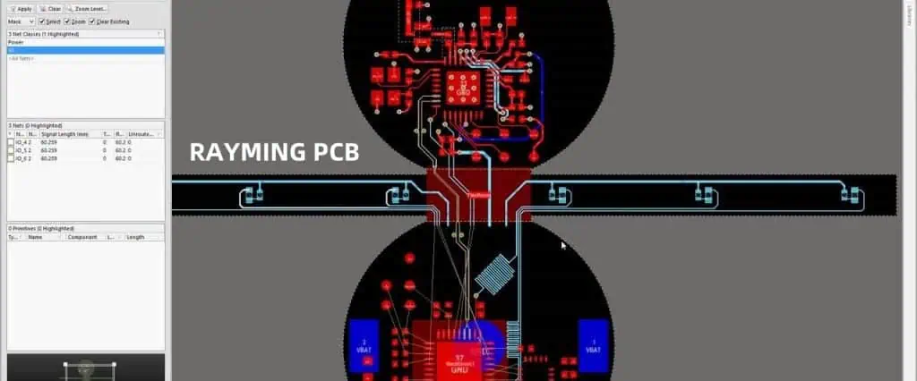
2. Differential Pair Routing

Differential signaling is highly effective in reducing EMI due to its inherent noise cancellation properties.

Best Practices for Differential Pair Routing

  1. Maintain consistent spacing between the pair
  2. Keep the pair tightly coupled throughout the route
  3. Avoid splits in the pair
  4. Match the length of each signal in the pair
  5. Use symmetrical via patterns for layer transitions

Differential Pair Spacing Guidelines

Differential ImpedanceTrace WidthTrace Spacing
85 Ohms5 mils5 mils
100 Ohms4 mils8 mils
120 Ohms3.5 mils12 mils

3. Controlled Impedance Routing

Maintaining consistent impedance along signal paths is crucial for minimizing reflections and EMI.

Techniques for Controlled Impedance Routing

  1. Use impedance calculators to determine trace geometries
  2. Maintain consistent trace widths and spacings
  3. Avoid abrupt changes in reference planes
  4. Use proper via design for impedance matching
  5. Implement proper termination strategies

Common Impedance Values and Corresponding Trace Widths

ImpedanceTrace Width (microstrip)Trace Width (stripline)
50 Ohms10 mils5 mils
75 Ohms5 mils3 mils
100 Ohms3 mils2 mils

4. Ground Plane Design and Via Stitching

Effective ground plane design is critical for EMI control in high-speed PCBs.

Ground Plane Best Practices

  1. Use solid ground planes whenever possible
  2. Avoid splitting ground planes under high-speed signals
  3. Implement ground plane stitching vias
  4. Ensure proper grounding of all components
  5. Use ground floods on signal layers judiciously

Via Stitching Guidelines

Signal FrequencyMaximum Via Spacing
< 100 MHz1/20 wavelength
100 MHz – 1 GHz1/40 wavelength
> 1 GHz1/60 wavelength

5. Power Distribution Network (PDN) Design

A well-designed PDN is essential for minimizing power-related EMI issues.

PDN Design Strategies

  1. Use dedicated power planes when possible
  2. Implement power plane stitching
  3. Use decoupling capacitors effectively
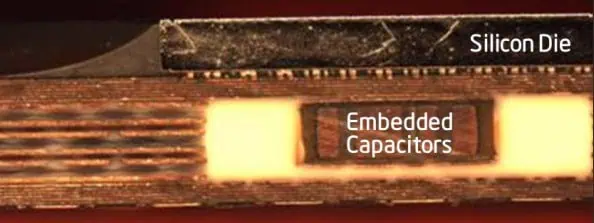
  4. Consider using embedded planar capacitance
  5. Optimize power trace routing for high-current paths

Decoupling Capacitor Selection Guide

Frequency RangeCapacitor Value
< 10 MHz10  ยตF – 100  ยตF
10 MHz – 100 MHz0.1  ยตF – 1  ยตF
100 MHz – 1 GHz1 nF – 10 nF
> 1 GHz100 pF – 1 nF

6. Signal Routing Techniques

Careful signal routing is crucial for minimizing EMI in high-speed designs.

Signal Routing Best Practices

  1. Keep high-speed traces short and direct
  2. Use 45-degree angles instead of 90-degree turns
  3. Route critical signals on inner layers
  4. Maintain proper clearances between signal groups
  5. Implement length matching for parallel buses

Recommended Trace Separation for Different Signal Types

GroupComponents
High-Speed DigitalMicroprocessors, FPGAs, High-speed memory
Low-Speed DigitalLow-frequency logic ICs, LEDs, Switches
AnalogOp-amps, ADCs, DACs, Sensors
PowerVoltage regulators, Power inductors, Bulk capacitors
I/OConnectors, Transceivers, Level shifters

7. Clock and Reset Signal Routing

Clock and reset signals require special attention due to their potential for generating EMI.

Clock Routing Techniques

  1. Use dedicated clock layers when possible
  2. Implement controlled impedance routing for clock signals
  3. Minimize the number of vias in clock paths
  4. Consider using differential clock distribution
  5. Implement proper termination for clock signals

Reset Signal Routing Guidelines

  1. Keep reset traces short and direct
  2. Avoid routing reset signals parallel to high-speed signals
  3. Use a star topology for reset distribution
  4. Consider using a dedicated reset controller IC

8. Shielding and Isolation Techniques

Implementing effective shielding and isolation can significantly reduce EMI in high-speed PCBs.

Board-Level Shielding Strategies

  1. Use guard traces around sensitive signals
  2. Implement moats and electromagnetic bandgaps
  3. Consider using buried stripline for critical signals
  4. Use shielding vias around board edges
  5. Implement faraday cages for sensitive circuits

Component-Level Isolation Techniques

  1. Use local ground islands for noisy components
  2. Implement split planes for analog and digital sections
  3. Use ferrite beads for power supply isolation
  4. Consider using optocouplers or digital isolators for crossing domain boundaries

9. EMI-Aware Component Placement

Strategic component placement can significantly impact EMI performance.

Component Placement Guidelines

  1. Group similar components together
  2. Keep noisy components away from sensitive circuits
  3. Place decoupling capacitors close to IC power pins
  4. Consider the direction of current flow in component placement
  5. Minimize the distance between differential pair components

Example Component Grouping Strategy

GroupComponentsHigh-Speed DigitalMicroprocessors, FPGAs, High-speed memoryLow-Speed DigitalLow-frequency logic ICs, LEDs, SwitchesAnalogOp-amps, ADCs, DACs, SensorsPowerVoltage regulators, Power inductors, Bulk capacitorsI/OConnectors, Transceivers, Level shifters

10. Post-Layout EMI Reduction Techniques

Even after careful layout, additional steps can be taken to further reduce EMI.

Post-Layout EMI Mitigation Strategies

  1. Perform EMI simulations and analysis
  2. Conduct pre-compliance testing
  3. Implement EMI filters on problematic signals
  4. Add ferrite beads or common-mode chokes on I/O lines
  5. Consider using spread spectrum clock generation

Common EMI Filter Configurations

Filter TypeConfigurationTypical Application
LC Low-PassSeries inductor, shunt capacitorPower supply lines
RC Low-PassSeries resistor, shunt capacitorDigital signal conditioning
Ferrite BeadSeries ferrite beadHigh-frequency noise suppression
Common-Mode ChokeCoupled inductorsDifferential pair EMI reduction

Conclusion

Mastering high-speed PCB routing techniques for EMI reduction is crucial in today’s electronic design landscape. By implementing the strategies outlined in this guide โ€“ from optimizing layer stack-ups and differential pair routing to careful power distribution and post-layout mitigation techniques โ€“ designers can significantly reduce the influence of EMI in their high-speed PCB designs.

Remember that EMI reduction is not a one-size-fits-all process. Each design may require a unique combination of techniques based on its specific requirements, constraints, and performance goals. Continuous learning, simulation, and testing are key to developing expertise in this critical area of PCB design.

By prioritizing EMI considerations throughout the design process, from initial component selection to final testing, engineers can create high-speed PCBs that not only meet performance requirements but also achieve electromagnetic compatibility, ensuring reliable operation in real-world environments.

Frequently Asked Questions (FAQ)

1. What is the most critical factor in reducing EMI in high-speed PCB designs?

While many factors contribute to EMI reduction, the most critical factor is often proper management of return currents. This involves:

  1. Using solid ground planes
  2. Maintaining signal-to-ground reference integrity
  3. Minimizing current loop areas
  4. Implementing effective via stitching

By ensuring well-defined, low-impedance return paths for all signals, designers can significantly reduce both conducted and radiated EMI.

2. How does differential signaling help in reducing EMI?

Differential signaling is highly effective in reducing EMI for several reasons:

  1. Common-mode noise rejection: Differential receivers respond to the difference between the two signals, naturally rejecting common-mode noise.
  2. Reduced loop area: The close proximity of differential pairs minimizes the loop area, reducing EMI emission and susceptibility.
  3. Cancellation of magnetic fields: The opposite currents in a differential pair create opposing magnetic fields that tend to cancel each other out.
  4. Lower amplitude: Differential signals typically use lower voltage swings, reducing the overall EMI potential.

These properties make differential signaling an excellent choice for high-speed, low-EMI designs.

3. What are some common mistakes in high-speed PCB routing that can lead to increased EMI?

Some common mistakes that can lead to increased EMI in high-speed PCB routing include:

  1. Neglecting proper layer stack-up design
  2. Routing high-speed signals over split planes
  3. Using 90-degree angles in trace routing
  4. Inadequate use of decoupling capacitors
  5. Improper termination of transmission lines
  6. Mixing analog and digital grounds improperly
  7. Neglecting proper shielding techniques
  8. Inconsistent impedance control
  9. Poor placement of components, especially clocks and oscillators
  10. Insufficient attention to power distribution network design

Avoiding these mistakes and adhering to best practices in high-speed PCB design can significantly reduce EMI issues.

4. How can I determine if my PCB design will pass EMC testing without expensive equipment?

While professional EMC testing is ultimately necessary for certification, there are several steps you can take to assess your design’s EMI performance without expensive equipment:

  1. Use EMI simulation software: Many PCB design tools offer EMI/EMC simulation capabilities.
  2. Perform near-field probing: Use low-cost near-field probes with an oscilloscope to identify EMI hotspots.
  3. Conduct functional testing in noisy environments: Test your product’s functionality in the presence of intentional electromagnetic disturbances.
  4. Use pre-compliance testing services: Some test labs offer lower-cost pre-compliance testing options.
  5. Implement design reviews: Have experienced designers review your layout for potential EMI issues.
  6. Follow established design guidelines: Adhering to industry best practices and guidelines can increase your chances of passing EMC testing.

Remember that while these methods can provide valuable insights, they are not substitutes for full EMC testing in a certified lab.

5. What are the key differences in EMI reduction techniques for digital versus analog circuits in a mixed-signal PCB?

While many EMI reduction techniques apply to both digital and analog circuits, there are some key differences in approach:

Digital Circuits:

  1. Focus on controlling edge rates and minimizing ringing
  2. Use of termination techniques to reduce reflections
  3. Emphasis on maintaining signal integrity through impedance control
  4. Clock distribution and synchronization are critical concerns
  5. Ground bounce and power supply noise are major issues

Analog Circuits:

  1. Greater emphasis on isolation and shielding
  2. Use of guard rings and ground planes for sensitive circuits
  3. Careful attention to grounding schemes (e.g., star grounding)
  4. Avoidance of high-frequency digital signals near analog circuits
  5. Use of differential signaling for noise-sensitive analog paths

In mixed-signal designs, the key is to effectively isolate the analog and digital sections while maintaining a cohesive grounding and power distribution strategy. This often involves techniques such as split planes, careful component placement, and strategic use of ferrite beads or other isolation components.

How to Evaluate A PCB Manufacturer or A PCB Assembler

In the rapidly evolving world of electronics, selecting the right Printed Circuit Board (PCB) manufacturer or assembler is crucial for the success of your project. Whether you’re a startup developing a new product or an established company looking to optimize your supply chain, the choice of PCB partner can significantly impact your product’s quality, cost, and time-to-market. This comprehensive guide will walk you through the essential factors to consider when evaluating PCB manufacturers and assemblers, helping you make an informed decision that aligns with your project requirements and business goals.

Understanding the Difference: PCB Manufacturer vs. PCB Assembler

Before diving into the evaluation process, it’s important to understand the distinction between a PCB manufacturer and a PCB assembler:

PCB Manufacturer

  • Focuses on producing bare PCBs
  • Handles processes like etching, drilling, and lamination
  • Typically does not deal with component placement or soldering

PCB Assembler

  • Specializes in populating PCBs with components
  • Manages processes such as surface-mount technology (SMT) and through-hole assembly
  • May offer additional services like functional testing and packaging

Some companies offer both manufacturing and prototype assembly services, while others specialize in one area. Your evaluation process may differ slightly depending on whether you’re looking for a manufacturer, an assembler, or a full-service provider.

Key Factors for Evaluation

multilayer pcb manufacturers

When assessing PCB manufacturers or assemblers, consider the following crucial factors:

1. Technical Capabilities

Manufacturing Capabilities (for PCB Manufacturers)

  • Board sizes and thicknesses
  • Layer count capabilities
  • Minimum trace width and spacing
  • Via types (through-hole, blind, buried)
  • Substrate materials offered
  • Special processes (e.g., flex PCB, rigid-flex)

Assembly Capabilities (for PCB Assemblers)

  • SMT capabilities (component sizes, pitch)
  • Through-hole assembly options
  • Mixed technology assembly
  • BGA and fine-pitch component handling
  • Specialized processes (e.g., conformal coating, potting)

2. Quality Management Systems

  • ISO 9001 certification
  • Industry-specific certifications (e.g., ISO 13485 for medical devices)
  • IPC standards compliance
  • In-house testing capabilities
  • Defect tracking and analysis processes

3. Production Capacity and Flexibility

  • Minimum and maximum order quantities
  • Turnaround times for prototypes and production runs
  • Ability to handle rush orders
  • Scalability for future production increases

4. Technology and Equipment

5. Experience and Expertise

  • Years in business
  • Industry focus and specializations
  • Experience with similar projects or technologies
  • Engineering support capabilities

6. Supply Chain Management

  • Component sourcing capabilities
  • Inventory management practices
  • Counterfeit prevention measures
  • Supply chain transparency

7. Communication and Customer Service

  • Responsiveness to inquiries
  • Technical support availability
  • Project management processes
  • Online ordering and tracking systems

8. Pricing and Cost Structure

  • Pricing for prototypes and production runs
  • Volume discounts
  • Payment terms
  • Hidden costs or fees

9. Location and Logistics

  • Geographic location
  • Shipping options and costs
  • Import/export considerations
  • Time zone compatibility for communication

10. Environmental and Social Responsibility

  • Environmental certifications (e.g., ISO 14001)
  • RoHS and REACH compliance
  • Sustainable practices
  • Labor practices and ethical standards

Evaluation Process

To effectively evaluate PCB manufacturers or assemblers, follow these steps:

1. Initial Research

  • Compile a list of potential partners
  • Review company websites and marketing materials
  • Check online reviews and testimonials
  • Seek recommendations from industry peers

2. Request for Information (RFI)

  • Prepare a detailed RFI document
  • Include project specifications and requirements
  • Ask for information on all relevant evaluation factors
  • Set a clear deadline for responses

3. Analysis of RFI Responses

  • Create a comparison matrix of responses
  • Identify strengths and weaknesses of each provider
  • Shortlist the most promising candidates

4. Site Visits and Audits

  • Arrange visits to shortlisted facilities
  • Observe manufacturing/assembly processes firsthand
  • Meet with key personnel
  • Conduct quality system audits if necessary

5. Request for Quotation (RFQ)

  • Provide detailed project specifications
  • Request quotes for prototypes and production runs
  • Ask for a breakdown of costs
  • Inquire about lead times and delivery options

6. Sample or Prototype Orders

  • Place small orders to test capabilities
  • Evaluate quality of delivered products
  • Assess communication and project management

7. Final Evaluation and Selection

  • Consider all factors holistically
  • Weigh the importance of each factor for your specific needs
  • Make a decision based on the best overall fit for your project

Comparison Table: Evaluating PCB Manufacturers vs. PCB Assemblers

To help visualize the differences in evaluation criteria between PCB manufacturers and assemblers, consider the following comparison table:

Evaluation Factor PCB Manufacturer PCB Assembler
Core Competency Bare PCB production Component placement and soldering
Key Technical Capabilities Layer count, trace width, via types Component sizes, SMT/THT processes
Quality Standards IPC-6010 series IPC-A-610
Equipment Focus Etching, drilling, pressing Pick-and-place machines, reflow ovens
Material Considerations PCB substrates, copper thickness Solder paste, flux
Design Support PCB layout optimization Component placement optimization
Testing Methods Electrical testing, impedance testing Functional testing, in-circuit testing
Supply Chain Involvement Limited to PCB materials Extensive component sourcing
Typical Lead Times Days to weeks Hours to days (for assembly only)
Cost Factors Material grade, layer count, finish Component costs, assembly complexity

Industry-Specific Considerations

Different industries may have unique requirements when evaluating PCB manufacturers or assemblers:

Automotive

  • IATF 16949 certification
  • Automotive-grade component sourcing
  • Stringent thermal and vibration testing

Aerospace and Defense

  • AS9100 certification
  • ITAR compliance (for U.S. companies)
  • Traceability and documentation requirements

Medical Devices

  • ISO 13485 certification
  • Clean room assembly capabilities
  • Biocompatibility considerations for materials

Consumer Electronics

  • High-volume production capabilities
  • Flexible scaling for seasonal demands
  • Rapid prototyping for fast time-to-market

Industrial and IoT Devices

  • Ruggedized design capabilities
  • Long-term availability of components
  • Experience with wireless technologies

Red Flags to Watch For

During your evaluation process, be alert for these potential warning signs:

  • Reluctance to provide references or facility tours
  • Outdated or poorly maintained equipment
  • Lack of proper certifications or quality systems
  • Inconsistent or evasive communication
  • Unusually low prices without justification
  • Inability to handle your specific technology requirements
  • Poor organization or cleanliness in production areas
  • High employee turnover or inexperienced staff

Building a Long-Term Partnership

Remember that selecting a PCB manufacturer or assembler is not just about finding a vendor for a single project. Ideally, you’re looking to establish a long-term partnership that can support your business as it grows and evolves. Consider these factors for building a lasting relationship:

  • Scalability of services
  • Willingness to invest in new technologies
  • Collaborative approach to problem-solving
  • Stability and financial health of the company
  • Alignment of business values and goals
  • Continuous improvement initiatives

Frequently Asked Questions (FAQ)

1. What’s the difference between a turnkey PCB assembly service and consigned assembly?

Turnkey PCB assembly is a comprehensive service where the assembler handles everything from PCB fabrication to component sourcing and final assembly. The customer provides only the design files and specifications. In consigned assembly, the customer provides both the PCBs and the components, and the assembler performs only the assembly process. Turnkey services offer more convenience but may be more expensive, while consigned assembly gives the customer more control over component selection and costs.

2. How important are certifications when evaluating a PCB manufacturer or assembler?

Certifications are crucial indicators of a company’s commitment to quality and industry standards. ISO 9001 is a baseline for quality management, while industry-specific certifications like ISO 13485 for medical devices or AS9100 for aerospace are essential for those sectors. However, certifications alone don’t guarantee performance โ€“ they should be considered alongside other factors like equipment, expertise, and track record.

3. What are the key differences in evaluating a domestic versus an overseas PCB partner?

When comparing domestic and overseas partners, consider factors such as:

  • Communication: Language barriers and time zone differences with overseas partners
  • Logistics: Shipping times and costs, import/export regulations
  • Intellectual property protection: Varying levels of IP law enforcement
  • Quality control: Potential need for more rigorous oversight with overseas partners
  • Cost: Generally lower labor costs overseas, but potentially higher shipping and management costs
  • Responsiveness: Potentially faster turnaround with local partners for prototypes or urgent needs

The best choice depends on your specific project requirements, budget, and risk tolerance.

4. How can I assess a PCB manufacturer’s or assembler’s technological capabilities without technical expertise?

If you lack in-house technical expertise, consider these approaches:

  • Request detailed capability statements and compare them to your project requirements
  • Ask for samples or case studies of similar projects they’ve completed
  • Engage a third-party consultant for an independent evaluation
  • Request references from current customers in your industry
  • Start with small prototype orders to assess capabilities firsthand

Remember, reputable manufacturers and assemblers should be willing to discuss their capabilities in terms you can understand and provide evidence of their expertise.

5. What are the most critical factors to consider for high-volume PCB production?

For high-volume PCB production, prioritize these factors:

  • Production capacity and scalability
  • Automated assembly capabilities
  • Quality control systems and defect rates
  • Supply chain robustness and component management
  • Cost-effectiveness and volume pricing
  • Consistency across large production runs
  • Ability to handle design revisions and product updates
  • Inventory management and just-in-time production capabilities

High-volume production requires a partner with not only the right equipment but also the processes and experience to maintain quality and efficiency at scale.

What is PCB Embedded Component Process?

The Printed Circuit Board (PCB) industry is constantly evolving, with new technologies and processes emerging to meet the demands of modern electronics. One such innovation is the PCB embedded component process, a technique that has gained significant attention in recent years. This article will delve into the intricacies of this process, exploring its benefits, challenges, and applications in various industries.

Understanding PCB Embedded Components

Definition and Concept

PCB embedded component process, also known as component embedding or embedded passive and active (EP&A) technology, refers to the practice of integrating electronic components directly into the layers of a printed circuit board during the manufacturing process. This technique differs from traditional surface-mount technology (SMT) or through-hole mounting, as components are literally embedded within the PCB structure itself.

Types of Embedded Components

Several types of components can be embedded in PCBs:

  1. Passive components
  2. Active components
  3. Other elements
    • Antennas
    • Sensors

The PCB Embedded Component Process

Step-by-Step Breakdown

The process of embedding components into PCBs involves several key steps:

  1. Design and planning
  2. Component preparation
  3. Cavity creation
  4. Component placement
  5. Lamination
  6. Via drilling and plating
  7. Outer layer circuitry
  8. Final testing and inspection

Let’s explore each of these steps in more detail.

1. Design and Planning

The embedded component process begins with careful design and planning. Engineers must consider factors such as:

  • Component selection
  • Optimal placement within PCB layers
  • Thermal management
  • Signal integrity
  • Manufacturing feasibility

Advanced PCB design software is typically used to create detailed layouts and simulations.

2. Component Preparation

Components intended for embedding often require special preparation:

  • Passive components may be supplied in sheet form
  • Active components might need thinning or special packaging
  • Some components may require additional protective coatings

3. Cavity Creation

Cavities are created in the PCB layers to accommodate the embedded components:

  • Laser ablation or mechanical milling techniques are commonly used
  • Precision is crucial to ensure proper fit and alignment

4. Component Placement

Components are carefully placed into the prepared cavities:

  • Automated pick-and-place machines or manual placement may be used
  • Alignment and orientation must be precise

5. Lamination

Once components are in place, additional PCB layers are laminated over them:

  • Heat and pressure are applied to bond the layers
  • Special care is taken to avoid damaging the embedded components

6. Via Drilling and Plating

Vias are drilled to create electrical connections:

  • Laser or mechanical drilling techniques are employed
  • Vias are plated to establish conductivity between layers

7. Outer Layer Circuitry

The outer layers of the PCB are processed:

  • Copper patterns are etched or plated
  • Additional surface-mount or through-hole components may be added

8. Final Testing and Inspection

Rigorous testing ensures the functionality and reliability of the embedded components:

Advantages of PCB Embedded Component Process

The embedded component process offers several significant advantages:

1. Miniaturization

By integrating components within the PCB layers, designers can achieve:

  • Reduced overall PCB size
  • Higher component density
  • More compact electronic devices

2. Improved Performance

Embedded components can lead to enhanced electrical performance:

  • Shorter signal paths
  • Reduced parasitic effects
  • Better signal integrity

3. Enhanced Reliability

The embedded nature of components provides protection:

  • Reduced exposure to environmental factors
  • Lower risk of mechanical stress
  • Improved thermal management

4. Cost Efficiency

While initial costs may be higher, embedded components can offer long-term savings:

  • Reduced assembly steps
  • Fewer external components needed
  • Potential for automation in manufacturing

5. Design Flexibility

Embedding components allows for greater design freedom:

  • Multi-functional PCB layers
  • Optimization of space utilization
  • Ability to create unique form factors

Challenges and Limitations

Despite its advantages, the PCB embedded component process faces several challenges:

1. Manufacturing Complexity

Embedding components requires specialized equipment and expertise:

  • Higher initial investment in manufacturing capabilities
  • More complex production processes
  • Increased potential for errors during manufacturing

2. Thermal Management

Heat dissipation can be more challenging with embedded components:

  • Limited access to components for cooling
  • Potential for hot spots within the PCB

3. Repairability and Rework

Embedded components are difficult or impossible to replace:

  • Limited options for repair
  • Entire PCB may need replacement in case of component failure

4. Testing and Quality Control

Inspecting and testing embedded components presents unique challenges:

  • Limited visual inspection possibilities
  • Need for advanced testing equipment (e.g., X-ray systems)

5. Cost Considerations

While there are potential long-term savings, initial costs can be higher:

  • Specialized manufacturing equipment required
  • Potentially lower yields, especially during initial implementation

Applications of PCB Embedded Component Process

The embedded component technology finds applications in various industries:

1. Consumer Electronics

  • Smartphones
  • Wearable devices
  • Tablets and laptops

2. Automotive Industry

  • Advanced driver assistance systems (ADAS)
  • Electric vehicle control units
  • Infotainment systems

3. Aerospace and Defense

  • Avionics systems
  • Satellite communications
  • Radar and electronic warfare equipment

4. Medical Devices

  • Implantable medical devices
  • Portable diagnostic equipment
  • Hearing aids

5. Industrial Applications

Future Trends and Developments

The PCB embedded component process continues to evolve:

1. Advanced Materials

Research into new materials for both PCBs and components:

  • High-frequency substrates
  • Thermally conductive materials
  • Flexible and stretchable substrates

2. 3D Printing Integration

Exploration of 3D printing technologies for PCB fabrication:

  • Potential for customized embedded components
  • Rapid prototyping capabilities

3. Artificial Intelligence and Machine Learning

AI and ML applications in design and manufacturing:

  • Optimized component placement
  • Predictive maintenance for manufacturing equipment
  • Enhanced quality control processes

4. Increased Automation

Further automation of the embedding process:

  • Improved precision and repeatability
  • Reduced manufacturing costs
  • Higher production volumes

5. Sustainability Efforts

Focus on environmentally friendly practices:

  • Development of recyclable PCB materials
  • Reduction of waste in the manufacturing process
  • Energy-efficient production methods

Comparison: Traditional PCB vs. Embedded Component PCB

To better understand the differences between traditional PCB assembly and the embedded component process, let’s compare key aspects:

AspectTraditional PCBEmbedded Component PCB
Component PlacementSurface-mount or through-holeWithin PCB layers
Board SizeLarger due to surface componentsCompact due to embedded components
Signal Path LengthLongerShorter
Electromagnetic InterferenceMore susceptibleReduced interference
Thermal ManagementEasier access for coolingMore challenging, requires careful design
Manufacturing ComplexityLowerHigher
Initial CostLowerHigher
Long-term CostPotentially higherPotentially lower
RepairabilityEasier to repair/replace componentsDifficult or impossible to repair
Design FlexibilityLimited by surface areaGreater 3D design possibilities

Frequently Asked Questions (FAQ)

1. What is the main difference between embedded components and surface-mount components?

Embedded components are integrated within the layers of the PCB during manufacturing, while surface-mount components are placed on the outer surfaces of the PCB after the board is fabricated. This key difference allows embedded components to create more compact designs with potentially better electrical performance.

2. Are all types of electronic components suitable for embedding in PCBs?

Not all components are suitable for embedding. Generally, passive components like resistors and capacitors are most commonly embedded. Some active components, such as certain ICs and semiconductors, can also be embedded if they meet specific size and packaging requirements. However, larger or more complex components may not be suitable for embedding due to size constraints or thermal management issues.

3. How does the PCB embedded component process affect the overall cost of manufacturing?

The embedded component process typically involves higher initial costs due to the need for specialized equipment and more complex manufacturing processes. However, it can lead to long-term cost savings through reduced assembly steps, fewer external components, and the potential for creating more compact devices. The cost-effectiveness often depends on the production volume and specific application requirements.

4. What are the main challenges in repairing or reworking PCBs with embedded components?

Repairing or reworking PCBs with embedded components is significantly more challenging than traditional PCBs. The main difficulties include:

  • Limited access to embedded components
  • Risk of damaging surrounding PCB layers during repair attempts
  • Inability to visually inspect embedded components
  • Lack of standardized repair procedures for embedded components

In many cases, if an embedded component fails, the entire PCB may need to be replaced rather than repaired.

5. How does the embedded component process impact the thermal management of a PCB?

Thermal management can be more complex with embedded components. While embedding can sometimes improve heat dissipation by allowing components to transfer heat directly to inner PCB layers, it can also create challenges:

  • Limited access to components for external cooling solutions
  • Potential for heat buildup within PCB layers
  • Need for careful thermal design and material selection

Designers must consider thermal management early in the design process, often using thermal simulation tools to optimize heat dissipation in embedded component PCBs.

How Decoupled Capacitance can be Obtained without Components

In the world of electronic design, decoupling capacitance plays a crucial role in maintaining signal integrity and power distribution. Traditionally, this has been achieved through the use of discrete capacitor components placed strategically on printed circuit boards (PCBs). However, as electronic devices continue to shrink in size and increase in complexity, engineers are seeking innovative ways to obtain decoupled capacitance without relying on additional components. This article explores the concept of achieving decoupled capacitance without components, focusing on techniques such as buried capacitance, integrated capacitance, and other emerging technologies.

Understanding Decoupled Capacitance

What is Decoupled Capacitance?

Decoupled capacitance refers to the practice of providing local charge storage near active devices on a PCB to mitigate the effects of rapid current demands and maintain stable voltage levels. This is typically achieved by placing capacitors close to the power pins of integrated circuits (ICs) to supply instantaneous current and reduce noise on power supply lines.

The Importance of Decoupling in Electronic Circuits

Decoupling is essential for several reasons:

  1. Noise reduction: It helps suppress high-frequency noise on power supply lines.
  2. Voltage stability: It maintains steady voltage levels during rapid current transitions.
  3. EMI reduction: It minimizes electromagnetic interference (EMI) emissions from the circuit.
  4. Improved performance: It enhances the overall performance and reliability of electronic systems.

Traditional Methods of Decoupling

Conventionally, decoupling has been achieved using discrete capacitor components. Here’s a brief overview of traditional decoupling methods:

MethodDescriptionAdvantagesLimitations
Surface-mount capacitorsSmall capacitors placed close to IC power pinsEasy to implement, wide range of values availableOccupies board space, parasitic inductance
Multi-layer ceramic capacitors (MLCCs)Compact capacitors with low ESR and ESLHigh capacitance density, good high-frequency performanceStill requires board real estate, potential for cracking
Capacitor arraysIntegrated packages containing multiple capacitorsSaves space compared to individual capacitorsLimited flexibility, potentially higher cost
Decoupling networksCombination of capacitors with different valuesProvides decouplin

While these methods have served the industry well, the push for miniaturization and higher performance has led to the exploration of component-less decoupling solutions.

Buried Capacitance Technology

Concept of Buried Capacitance

Buried capacitance is an innovative approach to achieving decoupled capacitance without the need for discrete components. It involves integrating capacitive structures directly into the PCB stack-up, creating a distributed capacitance throughout the board.

How Buried Capacitance Works

The principle behind buried capacitance is to create a thin dielectric layer between power and ground planes within the PCB. This forms a large, distributed capacitor that spans the entire board area. Here’s how it works:

  1. Thin dielectric layer: A very thin (typically less than 10 ฮผm) layer of high-permittivity material is used between power and ground planes.
  2. Large area: The entire overlap area of the power and ground planes contributes to the capacitance.
  3. Distributed nature: The capacitance is spread across the board, providing localized decoupling wherever needed.

Advantages of Buried Capacitance

Buried capacitance offers several benefits over traditional decoupling methods:

  1. Space-saving: Eliminates the need for numerous surface-mount capacitors, freeing up valuable board real estate.
  2. Improved performance: Lower inductance due to the distributed nature of the capacitance.
  3. Noise reduction: More effective at suppressing high-frequency noise.
  4. Simplified design: Reduces the complexity of component placement and routing.
  5. Cost-effective: Can potentially reduce overall manufacturing costs by eliminating components.

Implementation Challenges

While buried capacitance technology offers significant advantages, it also presents some challenges:

  1. Specialized materials: Requires high-permittivity, thin dielectric materials.
  2. Manufacturing process: Demands precise control of layer thicknesses and material properties.
  3. Design tools: Necessitates advanced PCB design tools that can model and simulate buried capacitance effects.
  4. Limited capacitance values: The achievable capacitance is constrained by board area and material properties.

Integrated Capacitance in Silicon

On-Chip Decoupling Capacitance

Another approach to obtaining decoupled capacitance without discrete components is to integrate it directly into the silicon of integrated circuits. This method, known as on-chip decoupling, involves creating capacitive structures within the IC itself.

Types of Integrated Capacitors

There are several types of integrated capacitors used for on-chip decoupling:

TypeDescriptionAdvantagesLimitations
MOS capacitorsUses the gate oxide of MOS transistorsHigh capacitance density, compatible with standard CMOS processesVoltage-dependent capacitance
Metal-insulator-metal (MIM) capacitorsUtilizes metal layers separated by a thin dielectricGood linearity, high Q-factorRequires additional process steps
Poly-insulator-poly (PIP) capacitorsUses polysilicon layers as electrodesCompatible with older process nodesLower capacitance density compared to MIM
Deep trench capacitorsVertical structures etched into the silicon substrateVery high capacitance densityComplex manufacturing process

Benefits of On-Chip Decoupling

Integrating decoupling capacitance on-chip offers several advantages:

  1. Proximity: Capacitance is located extremely close to the circuits that need it.
  2. Reduced parasitics: Minimizes inductance and resistance associated with external connections.
  3. Improved high-frequency performance: Better response to rapid current transients.
  4. Simplified PCB design: Reduces the need for external decoupling components.

Limitations and Considerations

While on-chip decoupling is beneficial, it has some limitations:

  1. Limited capacitance: The amount of on-chip capacitance is constrained by die area and process technology.
  2. Cost: Integrating large amounts of capacitance can increase die size and cost.
  3. Process complexity: Some integrated capacitor types require additional manufacturing steps.
  4. Design complexity: Requires careful consideration during IC design and layout.

Advanced PCB Materials and Structures for Component-less Decoupling

High-k Dielectric Materials

One of the key enablers of component-less decoupling is the development of high-k dielectric materials. These materials have a higher dielectric constant (k) than traditional PCB substrates, allowing for greater capacitance in a given area.

Properties of High-k Materials

Here’s a comparison of some common PCB dielectric materials and their properties:

MaterialDielectric Constant (k)Typical ThicknessCapacitance Density
FR-44.0-4.5100-200 ฮผmLow
High-k Laminates10.-3050-100 ฮผmMedium
Ceramic-filled Epoxy30-5025-75 ฮผmHigh
Thin-film Ceramics100-10001-10 ฮผmVery High

Advantages of High-k Materials for Decoupling

  1. Increased capacitance density
  2. Improved power integrity
  3. Reduced layer count in PCB stack-ups
  4. Enhanced high-frequency performance

Challenges in Implementation

  1. Higher material costs
  2. Potential for increased signal loss
  3. Manufacturing process adaptations
  4. Design tool limitations for accurate modeling

Embedded Planar Capacitance

Embedded planar capacitance takes the concept of buried capacitance further by incorporating specialized materials and structures within the PCB stack-up.

Structure of Embedded Planar Capacitance

  1. Ultra-thin dielectric layer (typically 2-20 ฮผm)
  2. Large area copper planes on both sides of the dielectric
  3. Integration into standard PCB manufacturing processes

Benefits of Embedded Planar Capacitance

  1. Very high capacitance density (up to 10 nF/cmยฒ)
  2. Excellent high-frequency decoupling performance
  3. Reduced PCB layer count
  4. Improved signal integrity and EMI suppression

Design Considerations

  1. Careful power plane segmentation
  2. Proper via placement for effective charge distribution
  3. Consideration of thermal management implications
  4. Integration with other PCB design elements (e.g., signal routing)

Interdigitated Capacitance Structures

Interdigitated capacitance structures offer another approach to achieving component-less decoupling by utilizing the PCB’s existing copper layers.

How Interdigitated Structures Work

  1. Alternating finger-like extensions of power and ground planes
  2. Increased edge coupling between adjacent fingers
  3. Utilization of fringing electric fields for capacitance

Advantages of Interdigitated Structures

  1. Can be implemented with standard PCB materials
  2. No need for specialized ultra-thin dielectrics
  3. Flexible design options for targeted decoupling
  4. Compatible with both rigid and flexible PCB technologies

Design Trade-offs

  1. Reduced plane area for current distribution
  2. Potential for increased crosstalk in nearby signal traces
  3. Complexity in optimizing finger dimensions and spacing
  4. Limited total capacitance compared to other methods

Hybrid Approaches

In practice, achieving optimal decoupling often involves a combination of techniques. Hybrid approaches leverage the strengths of multiple methods to create a comprehensive decoupling solution.

Combining Techniques

  1. Buried capacitance + strategic discrete components
  2. On-chip decoupling + embedded planar capacitance
  3. Interdigitated structures + high-k materials

Benefits of Hybrid Solutions

  1. Tailored decoupling for different frequency ranges
  2. Optimized performance-cost trade-off
  3. Flexibility in addressing specific design requirements
  4. Improved overall system performance

Design and Simulation Techniques

Implementing component-less decoupling requires advanced design and simulation techniques to ensure optimal performance.

Electromagnetic Field Simulation

Electromagnetic field simulation is crucial for accurately predicting the behavior of component-less decoupling structures.

Key Aspects of EM Simulation

  1. Full-wave analysis of PCB stack-up
  2. Modeling of complex material properties
  3. Extraction of distributed capacitance and inductance
  4. Prediction of resonances and anti-resonances

Tools and Methodologies

  1. Finite Element Method (FEM) solvers
  2. Method of Moments (MoM) tools
  3. Hybrid simulation techniques
  4. Multi-physics simulations for thermal considerations

Power Integrity Analysis

Power integrity analysis is essential for evaluating the effectiveness of component-less decoupling solutions.

Elements of Power Integrity Analysis

  1. DC IR drop analysis
  2. AC impedance profiling
  3. Time-domain transient simulations
  4. Frequency-domain resonance analysis

Performance Metrics

MetricDescriptionTarget Values
Target ImpedanceMaximum acceptable power distribution network impedanceTypically 1-10 mๆƒŸ
Voltage RipplePeak-to-peak voltage variation on power rails< 5% of nominal voltage
Resonant FrequenciesFrequencies at which the power delivery network resonatesShould be outside operating frequency range
Decoupling EffectivenessMeasure of how well the decoupling solution suppresses noise> 20 dB atten

Optimization Techniques

Optimizing component-less decoupling designs often requires sophisticated algorithms and methodologies.

Optimization Approaches

  1. Genetic algorithms for layout optimization
  2. Machine learning-based material selection
  3. Multi-objective optimization for balancing performance and cost
  4. Sensitivity analysis for identifying critical design parameters

Design for Manufacturability (DFM) Considerations

  1. Layer stack-up optimization
  2. Via placement and sizing strategies
  3. Copper balancing techniques
  4. Alignment with PCB fabrication capabilities

Practical Implementation and Case Studies

To illustrate the real-world application of component-less decoupling, let’s examine some case studies and practical implementation strategies.

Case Study 1: High-Speed Digital PCB

In this case study, a high-speed digital PCB for a telecommunications application utilized embedded planar capacitance to achieve superior decoupling performance.

Design Approach

  1. Utilization of 4 ฮผm thick high-k dielectric layer
  2. Strategic segmentation of power planes
  3. Optimized via placement for charge distribution
  4. Hybrid solution with minimal strategic discrete capacitors

Results

  1. 50% reduction in discrete decoupling capacitors
  2. 30% improvement in power supply noise rejection
  3. 20% reduction in overall PCB thickness
  4. Significant improvement in signal integrity margins

Case Study 2: Mixed-Signal Automotive PCB

This case study focuses on a mixed-signal automotive PCB that employed a combination of buried capacitance and interdigitated structures.

Implementation Strategy

  1. Buried capacitance for global power distribution
  2. Interdigitated structures for localized high-frequency decoupling
  3. Careful isolation of analog and digital power domains
  4. Use of EM simulation for optimizing interdigitated patterns

Outcomes

  1. Elimination of 80% of surface-mount decoupling capacitors
  2. Improved EMI performance, meeting stringent automotive standards
  3. Enhanced reliability due to reduced component count
  4. 15% reduction in overall PCB cost

Best Practices for Implementation

Based on these case studies and industry experience, here are some best practices for implementing component-less decoupling:

  1. Start with accurate EM and power integrity simulations
  2. Consider hybrid approaches for optimal performance
  3. Pay close attention to manufacturing tolerances and their impact
  4. Validate designs through prototyping and extensive testing
  5. Stay informed about emerging materials and technologies
  6. Collaborate closely with PCB manufacturers to ensure feasibility

Future Trends and Emerging Technologies

The field of component-less decoupling is continuously evolving. Here are some future trends and emerging technologies to watch:

  1. Advanced nanomaterials for ultra-high-k dielectrics
  2. 3D-printed embedded capacitance structures
  3. Integration of decoupling solutions with active power management systems
  4. Machine learning-driven optimization of decoupling designs
  5. Adoption of component-less decoupling in flexible and stretchable electronics

As these technologies mature, we can expect even more efficient and effective component-less decoupling solutions in the future.

Frequently Asked Questions (FAQ)

  1. Q: Can component-less decoupling completely eliminate the need for discrete capacitors? A: While component-less decoupling can significantly reduce the number of discrete capacitors, it may not completely eliminate them in all cases. Some designs may still require a few strategic discrete components for optimal performance, especially at very high frequencies or for bulk decoupling.
  2. Q: How does the cost of component-less decoupling compare to traditional methods? A: The cost comparison depends on various factors, including production volume, PCB complexity, and specific implementation. While component-less solutions may have higher initial material costs, they often lead to overall cost savings through reduced component count, improved reliability, and simplified assembly processes.
  3. Q: Are there any reliability concerns with component-less decoupling techniques? A: Generally, component-less decoupling can improve reliability by reducing the number of solder joints and potential points of failure. However, it’s crucial to consider factors such as thermal cycling, moisture sensitivity, and long-term stability of the specialized materials used.
  4. Q: How does component-less decoupling affect PCB manufacturability? A: Component-less decoupling may require adjustments to standard PCB manufacturing processes, particularly when using very thin dielectric layers or specialized materials. Close collaboration with PCB manufacturers is essential to ensure producibility and yield.
  5. Q: Can component-less decoupling techniques be applied to flexible PCBs? A: Yes, many component-less decoupling techniques can be adapted for flexible PCBs. Techniques like interdigitated structures and some forms of buried capacitance are particularly suitable for flexible circuits, offering decoupling solutions without compromising flexibility.

This concludes the article on how decoupled capacitance can be obtained without components. The content covers the concept, various techniques, implementation challenges, design considerations, and future trends in component-less decoupling for PCBs.

How to Maintain a Reflow Oven

Reflow ovens are critical components in the surface mount technology (SMT) assembly process, playing a crucial role in the production of printed circuit boards (PCBs). These sophisticated machines are responsible for soldering surface mount components to PCBs by precisely controlling temperature profiles. To ensure consistent, high-quality results and maximize the lifespan of the equipment, proper maintenance of reflow ovens is essential.

In this comprehensive guide, we will explore the best practices for maintaining a reflow oven, covering everything from routine cleaning procedures to advanced troubleshooting techniques. By following these guidelines, you can optimize your reflow oven’s performance, reduce downtime, and ultimately improve the quality of your PCB assemblies.

Understanding Reflow Oven Basics

Types of Reflow Ovens

Before delving into maintenance procedures, it’s important to understand the different types of reflow ovens commonly used in the industry:

  1. Convection Reflow Ovens: These use forced hot air to heat the PCBs and components.
  2. Infrared (IR) Reflow Ovens: These use infrared radiation for heating.
  3. Vapor Phase Reflow Ovens: These use the latent heat of vaporization of a special liquid to heat the assemblies.

Each type has its own specific maintenance requirements, but many general principles apply across all types.

Key Components of a Reflow Oven

To effectively maintain a reflow oven, it’s crucial to understand its main components:

ComponentFunction
Heating ElementsGenerate heat for the soldering process
Conveyor SystemMoves PCBs through the oven
Control SystemManages temperature profiles and oven operation
Cooling SystemCools PCBs after reflow
Exhaust SystemRemoves fumes and maintains internal atmosphere
SensorsMonitor temperature, conveyor speed, and other parameters

Routine Maintenance Procedures

Daily Maintenance Tasks

Performing daily maintenance tasks is crucial for keeping your reflow oven in optimal condition:

  1. Visual Inspection
    • Check for any visible damage or wear
    • Inspect conveyor belts for proper tension and alignment
    • Look for any debris or flux residue buildup
  2. Clean Conveyor System
    • Use a soft brush or vacuum to remove loose particles
    • Wipe down conveyor belts with an appropriate cleaning solution
  3. Check Temperature Sensors
    • Ensure all sensors are securely in place
    • Look for any signs of damage or corrosion
  4. Verify Exhaust System Operation
    • Check that exhaust fans are running smoothly
    • Listen for any unusual noises

Weekly Maintenance Tasks

In addition to daily tasks, perform these maintenance procedures on a weekly basis:

  1. Deep Clean Oven Interior
    • Remove and clean all removable parts (e.g., nozzles, filters)
    • Use manufacturer-approved cleaning agents to remove flux residue
    • Pay special attention to heating elements and corners where residue accumulates
  2. Inspect and Clean Cooling System
    • Check coolant levels if applicable
    • Clean cooling fans and heat exchangers
  3. Calibrate Temperature Sensors
    • Use a calibrated thermocouple to verify sensor accuracy
    • Adjust or replace sensors as necessary
  4. Check and Tighten Electrical Connections
    • Inspect all accessible electrical connections
    • Tighten any loose connections to prevent arcing or failure

Monthly Maintenance Tasks

Monthly maintenance involves more thorough checks and preventive measures:

  1. Lubricate Moving Parts
    • Apply lubricant to conveyor bearings and other moving components
    • Follow manufacturer guidelines for appropriate lubricants
  2. Check and Replace Filters
    • Inspect and clean or replace air filters
    • Check and replace exhaust filters if necessary
  3. Verify Profile Accuracy
    • Run test boards with thermocouples to ensure profile accuracy
    • Make adjustments to the control system if needed
  4. Inspect Heating Elements
    • Check for any signs of wear, discoloration, or damage
    • Replace elements if necessary to maintain even heating

Advanced Maintenance Procedures

Quarterly Maintenance Tasks

Perform these more intensive maintenance procedures every three months:

  1. Comprehensive Cleaning
    • Disassemble oven components for thorough cleaning
    • Use specialized cleaning agents to remove stubborn residues
    • Clean and inspect areas not easily accessible during routine maintenance
  2. Heating Element Inspection and Testing
    • Conduct resistance tests on heating elements
    • Check for any hot spots or uneven heating
    • Replace elements that show signs of degradation
  3. Control System Diagnostics
    • Run full system diagnostics to check for any errors or anomalies
    • Update software if newer versions are available
    • Verify all control parameters are within specification
  4. Exhaust System Overhaul
    • Clean exhaust ducts thoroughly
    • Inspect and replace gaskets and seals
    • Verify proper airflow and adjust if necessary

Annual Maintenance Tasks

Annually, conduct a complete overhaul of the reflow oven:

  1. Full System Inspection
    • Thoroughly inspect all components for wear and tear
    • Document any parts that may need replacement in the near future
  2. Calibration of All Systems
    • Recalibrate temperature sensors, conveyor speed, and other critical parameters
    • Verify calibration with certified test equipment
  3. Electrical System Check
    • Conduct a comprehensive check of all electrical systems
    • Test insulation resistance and ground continuity
    • Replace any worn wiring or components
  4. Mechanical System Overhaul
    • Inspect and replace worn bearings, belts, and other mechanical components
    • Realign conveyor system if necessary
  5. Safety System Verification
    • Test all safety interlocks and emergency stop functions
    • Verify proper operation of overtemperature protection systems

Maintenance Best Practices

To ensure the longevity and optimal performance of your reflow oven, consider the following best practices:

  1. Create a Maintenance Schedule
    • Develop a detailed maintenance calendar
    • Assign responsibilities to specific team members
    • Use maintenance management software for tracking and reminders
  2. Train Operators and Maintenance Staff
    • Provide comprehensive training on oven operation and maintenance procedures
    • Regularly update training to cover new techniques or equipment updates
  3. Keep Detailed Maintenance Records
    • Document all maintenance activities, including date, tasks performed, and parts replaced
    • Use these records to identify recurring issues and plan preventive maintenance
  4. Use High-Quality Replacement Parts
    • Always use manufacturer-recommended or equivalent quality parts
    • Avoid generic replacements that may compromise performance or safety
  5. Monitor Performance Metrics
    • Track key performance indicators such as temperature stability and profile accuracy
    • Use data to identify trends and potential issues before they become critical
  6. Implement Predictive Maintenance Techniques
    • Utilize advanced monitoring tools to predict potential failures
    • Analyze data patterns to optimize maintenance schedules

By following these maintenance procedures and best practices, you can significantly extend the life of your reflow oven, minimize downtime, and ensure consistent, high-quality PCB production.

Troubleshooting Common Reflow Oven Issues

Even with regular maintenance, reflow ovens may occasionally experience problems. Here are some common issues and their potential solutions:

Temperature Control Problems

Symptom: Inconsistent or Inaccurate Temperature Profiles

Possible causes and solutions:

  1. Faulty Temperature Sensors
    • Test sensors for accuracy
    • Replace if damaged or out of calibration
  2. Degraded Heating Elements
    • Check for uneven heating patterns
    • Replace elements showing signs of wear
  3. Control System Malfunction
    • Run system diagnostics
    • Update software or replace faulty control boards

Symptom: Overheating or Failure to Reach Target Temperature

Possible causes and solutions:

  1. Stuck Relays or Solid State Devices
    • Test and replace faulty components
  2. Airflow Issues
    • Check for blocked vents or faulty fans
    • Clean or replace as necessary
  3. Incorrect PID Settings
    • Review and adjust PID parameters
    • Consult manufacturer guidelines for optimal settings

Conveyor System Problems

Symptom: Uneven Board Movement or Conveyor Stoppages

Possible causes and solutions:

  1. Belt Tension Issues
    • Adjust belt tension according to specifications
    • Replace belts if worn or damaged
  2. Motor or Drive System Failure
    • Check motor and gearbox for signs of wear
    • Replace damaged components
  3. Misaligned Conveyor Rails
    • Realign rails to ensure smooth board movement
    • Check for and remove any obstructions

Exhaust System Issues

Symptom: Poor Fume Extraction or Unusual Odors

Possible causes and solutions:

  1. Clogged Filters
    • Clean or replace air and exhaust filters
  2. Faulty Exhaust Fan
    • Check fan operation and replace if necessary
  3. Leaks in Exhaust Ducting
    • Inspect ductwork for leaks or damage
    • Seal or replace as needed

Profile Accuracy Problems

Symptom: Inconsistent Solder Quality Across Boards

Possible causes and solutions:

  1. Uneven Heat Distribution
    • Check for blocked or dirty heating nozzles
    • Verify proper operation of all heating zones
  2. Incorrect Profile Settings
    • Review and adjust profile parameters
    • Use profiling equipment to verify and optimize settings
  3. Board Warpage Issues
    • Adjust conveyor speed or zone temperatures
    • Consider using board supports for large or thin PCBs

Maintenance Tools and Equipment

To effectively maintain a reflow oven, certain tools and equipment are essential:

Tool/EquipmentPurpose
Thermocouple ProfilerAccurately measure and record temperature profiles
Infrared ThermometerQuick spot-checking of surface temperatures
MultimeterTesting electrical components and connections
Cleaning SuppliesSpecialized solvents and tools for removing flux residue
Safety EquipmentGloves, eye protection, and respirators for handling chemicals
Calibration EquipmentDevices for calibrating temperature sensors and other instruments
Diagnostic SoftwareFor running system checks and analyzing performance data

Frequently Asked Questions (FAQ)

  1. Q: How often should I clean my reflow oven? A: Basic cleaning should be performed daily, with more thorough cleaning on a weekly basis. Deep cleaning and inspection should be done monthly or quarterly, depending on usage.
  2. Q: What are the signs that my reflow oven needs maintenance? A: Signs include inconsistent soldering results, temperature fluctuations, unusual noises from the conveyor or fans, and visible buildup of flux residue or debris inside the oven.
  3. Q: Can I use regular cleaning agents to clean my reflow oven? A: No, it’s important to use cleaning agents specifically designed for reflow ovens. Regular cleaning agents may leave residues that can affect soldering quality or damage oven components.
  4. Q: How long does a typical reflow oven last with proper maintenance? A: With proper maintenance, a reflow oven can last 10-15 years or more. However, technological advancements may make upgrading desirable before the end of the oven’s physical lifespan.
  5. Q: Is it necessary to keep detailed maintenance records? A: Yes, detailed records are crucial. They help in identifying recurring issues, planning preventive maintenance, and can be valuable for troubleshooting or when seeking technical support from the manufacturer.

Conclusion

Maintaining a reflow oven is a critical aspect of ensuring consistent, high-quality PCB production. By following a comprehensive maintenance schedule that includes daily, weekly, monthly, and annual tasks, you can significantly extend the life of your equipment and minimize costly downtime.

Remember that proper maintenance goes beyond just cleaning and replacing parts. It involves a holistic approach that includes operator training, performance monitoring, and proactive troubleshooting. By implementing the best practices outlined in this guide, you can optimize your reflow oven’s performance, improve production efficiency, and maintain the high standards required in modern electronics manufacturing.

Always consult your oven’s specific manufacturer guidelines for detailed maintenance procedures, and don’t hesitate to seek professional assistance for complex issues or major overhauls. With diligent care and attention, your reflow oven will continue to be a reliable workhorse in your SMT assembly line for years to come.

How Does 3D Automated Optical Inspection work in the PCB Assembly Process

In the ever-evolving world of electronics manufacturing, quality control plays a crucial role in ensuring the reliability and functionality of printed circuit boards (PCBs). As PCB designs become increasingly complex and miniaturized, traditional inspection methods are often insufficient to detect all potential defects. This is where 3D Automated Optical Inspection (AOI) comes into play, revolutionizing the PCB assembly process with its advanced capabilities and precision.

3D AOI technology has emerged as a game-changer in the electronics industry, offering a comprehensive and highly accurate method for inspecting PCBs at various stages of production. By combining cutting-edge optical systems, sophisticated algorithms, and three-dimensional imaging techniques, 3D AOI systems can detect a wide range of defects that might otherwise go unnoticed until final testing or, worse, after the product reaches the end-user.

In this article, we will delve deep into the workings of 3D Automated Optical Inspection in the PCB assembly process. We’ll explore its core principles, key components, and the step-by-step procedure it follows to ensure the highest quality standards in PCB manufacturing. Additionally, we’ll discuss the advantages of 3D AOI over traditional inspection methods and its impact on production efficiency and product reliability.

Understanding 3D Automated Optical Inspection

What is 3D AOI?

3D Automated Optical Inspection is an advanced quality control technique used in the PCB assembly process to detect and identify defects on printed circuit boards. Unlike traditional 2D AOI systems, which rely solely on top-down imaging, 3D AOI utilizes multiple cameras and advanced lighting techniques to create a three-dimensional representation of the PCB and its components.

This technology allows for a more comprehensive inspection, capable of detecting issues such as:

  1. Component placement errors
  2. Solder joint defects
  3. Missing or incorrect components
  4. Board warpage
  5. Component height variations
  6. Coplanarity issues

Key Components of a 3D AOI System

To understand how 3D AOI works, it’s essential to familiarize ourselves with its key components:

  1. Multiple High-Resolution Cameras: These capture images of the PCB from various angles.
  2. Structured Light Projectors: They project patterns onto the PCB surface to create 3D profiles.
  3. Advanced Lighting Systems: Including LED arrays and laser modules for optimal illumination.
  4. High-Speed Image Processing Unit: Analyzes the captured images in real-time.
  5. Sophisticated Software Algorithms: Interpret the data and identify defects based on predefined criteria.
  6. Conveyor System: Moves PCBs through the inspection area.
  7. User Interface: Allows operators to configure settings and review inspection results.

The Evolution from 2D to 3D AOI

To appreciate the capabilities of 3D AOI, it’s helpful to understand its evolution from 2D systems:

Aspect2D AOI3D AOI
ImagingSingle top-down viewMultiple angles and 3D profiling
Defect DetectionSurface-level defectsSurface and volumetric defects
Component InspectionLimited to visible surfacesComprehensive, including hidden solder joints
AccuracyGood for basic defectsExcellent, with reduced false calls
Solder Joint InspectionLimited capabilityHighly accurate and detailed
Coplanarity CheckingNot possibleFully capable
Data Output2D images and measurements3D models and precise volumetric data

This comparison highlights the significant advancements that 3D AOI brings to the PCB inspection process, enabling a more thorough and accurate quality control procedure.

The Working Principle of 3D AOI in PCB Assembly

SMT AOI
SMT AOI

Data Acquisition

The first step in the 3D AOI process is data acquisition. This phase involves capturing detailed images and creating a three-dimensional profile of the PCB under inspection. Here’s how it works:

  1. Multiple Camera Imaging: The PCB is photographed from various angles using high-resolution cameras. These images provide a comprehensive view of the board’s surface and components.
  2. Structured Light Projection: Patterns of light are projected onto the PCB surface. By analyzing how these patterns deform when projected onto three-dimensional objects, the system can create a detailed 3D map of the board.
  3. Laser Triangulation: In some systems, laser beams are used to measure the height and profile of components with high precision.
  4. Shadow Moirรฉ Technology: This technique uses the interference patterns created by a reference grating and its shadow on the PCB to measure surface topography accurately.

The combination of these techniques allows the 3D AOI system to gather a wealth of data about the PCB’s physical characteristics, far beyond what is possible with traditional 2D inspection methods.

Image Processing and Analysis

Once the raw data is acquired, the 3D AOI system processes and analyzes it to identify potential defects. This stage involves several sophisticated algorithms and techniques:

  1. Image Enhancement: Raw images are processed to improve contrast, reduce noise, and highlight features of interest.
  2. 3D Reconstruction: The system combines data from multiple sources to create a detailed 3D model of the PCB.
  3. Feature Extraction: Key features such as component edges, solder joints, and pad locations are identified and isolated for further analysis.
  4. Pattern Matching: The observed features are compared against a database of known good examples or CAD data to identify discrepancies.
  5. Defect Classification: Any anomalies detected are classified into specific types of defects based on predefined criteria.

Defect Detection and Classification

The 3D AOI system is capable of detecting and classifying a wide range of defects. Here’s a table outlining some common defect types and how 3D AOI detects them:

Defect TypeDetection Method
Component MisalignmentComparison of actual vs. expected position in 3D space
Solder Joint IssuesAnalysis of solder joint shape, volume, and surface characteristics
Missing ComponentsAbsence of expected 3D features in component locations
Incorrect ComponentsMismatch between observed and expected 3D profiles
Lifted LeadsDetection of abnormal height or angle of component leads
TombstoningIdentification of components standing on end instead of lying flat
Solder BridgingDetection of unexpected solder connections between pads
Insufficient SolderMeasurement of solder volume and coverage
Board WarpageAnalysis of overall PCB planarity
Foreign Object DebrisIdentification of unexpected 3D objects on the board surface

This comprehensive defect detection capability is one of the key advantages of 3D AOI over traditional inspection methods.

Result Reporting and Integration

After the inspection process, the 3D AOI system generates detailed reports of its findings. These reports typically include:

  1. High-resolution images of detected defects
  2. 3D renderings of problem areas
  3. Precise measurements and location data for each defect
  4. Statistical data on defect types and frequencies

Modern 3D AOI systems are often integrated into the broader manufacturing execution system (MES), allowing for real-time data sharing and process control. This integration enables:

  1. Immediate feedback to upstream processes for defect prevention
  2. Automatic routing of defective boards to repair stations
  3. Collection of long-term data for process improvement initiatives
  4. Traceability of individual boards throughout the manufacturing process

In the next section, we’ll explore the specific steps involved in setting up and operating a 3D AOI system in a PCB assembly line.

How to Export Gerber Files from AutoCAD

In the world of printed circuit board (PCB) design and manufacturing, Gerber files play a crucial role. These files contain all the necessary information for PCB fabrication, including layer stackup, copper traces, drill holes, and more. AutoCAD, a popular computer-aided design (CAD) software, is often used for PCB design. However, exporting Gerber files from AutoCAD requires specific steps and considerations. This comprehensive guide will walk you through the process of exporting Gerber files from AutoCAD, ensuring your PCB designs are ready for production.

Understanding Gerber Files

What are Gerber Files?

Gerber files are a set of standardized file formats used in the PCB industry to describe the layers of a printed circuit board. Named after Gerber Systems Corporation (now part of Ucamco), these files contain vector-based images that represent different aspects of a PCB design.

Types of Gerber Files

There are several types of Gerber files, each serving a specific purpose in PCB fabrication:

File TypeDescriptionCommon Extension
Top CopperRepresents the copper layer on the top of the PCB.GTL
Bottom CopperRepresents the copper layer on the bottom of the PCB.GBL
Top Solder MaskDefines areas where solder mask should not be applied on the top.GTS
Bottom Solder MaskDefines areas where solder mask should not be applied on the bottom.GBS
Top SilkscreenContains text and component outlines for the top of the PCB.GTO
Bottom SilkscreenContains text and component outlines for the bottom of the PCB.GBO
Drill FileSpecifies the location and size of drill holes.TXT or .XLN

Importance of Gerber Files in PCB Manufacturing

Gerber files are essential for several reasons:

  1. Standardization: They provide a universal format that PCB manufacturers worldwide can understand and use.
  2. Accuracy: Gerber files ensure that the PCB design is accurately translated from the CAD software to the manufacturing process.
  3. Layer separation: Each aspect of the PCB design is contained in a separate file, allowing for easy modification and error checking.
  4. Manufacturing flexibility: Gerber files can be used with various PCB manufacturing equipment, regardless of the original design software.

Preparing AutoCAD for Gerber Export

Before you can export Gerber files from AutoCAD, you need to ensure that your design is properly set up and that you have the necessary tools installed.

Required AutoCAD Version and Add-ons

To export Gerber files from AutoCAD, you’ll need:

  1. AutoCAD (preferably the latest version)
  2. A PCB design add-on or plugin (e.g., AutoCAD Electrical or a third-party plugin)

Setting Up Your PCB Design in AutoCAD

Follow these steps to prepare your PCB design for Gerber export:

  1. Create separate layers for each aspect of your PCB design (e.g., top copper, bottom copper, silkscreen).
  2. Use appropriate line types and colors to distinguish between different features.
  3. Ensure all components are properly placed and connected.
  4. Double-check your design for any errors or inconsistencies.

Configuring Units and Scale

Proper unit and scale configuration is crucial for accurate Gerber file export:

  1. Set the drawing units to millimeters or inches, depending on your preference and manufacturing requirements.
  2. Ensure that the scale of your design matches the intended physical size of the PCB.
  3. Verify that all components and traces are drawn to the correct scale.

Exporting Gerber Files from AutoCAD

Now that your design is prepared, let’s go through the process of exporting Gerber files from AutoCAD.

Step-by-Step Export Process

1. Open the PCB Design File

Open your PCB design file in AutoCAD. Ensure that all layers are visible and that the design is complete.

2. Access the Export Function

The exact method to access the Gerber export function may vary depending on your AutoCAD version and installed plugins. Generally, you’ll find it under:

  • File > Export > Gerber Files
  • Or through a dedicated PCB design toolbar or ribbon

3. Select Layers to Export

In the export dialog:

  1. Choose which layers you want to export as Gerber files.
  2. Specify the output folder where the Gerber files will be saved.
  3. Set the file naming convention for each layer (e.g., ProjectName_TopCopper.GTL).

4. Configure Export Settings

Adjust the following settings for optimal Gerber file export:

SettingRecommended ValueDescription
UnitsMM or InchesMatch your design units
Format2:4 or 4:4Coordinate format (integer:decimal)
Zero SuppressionLeading or TrailingHow to handle leading/trailing zeros
Aperture TypeGerber (RS-274X)Modern Gerber format
Output PolarityPositiveStandard for most designs

5. Generate Drill Files

In addition to the Gerber files, you’ll need to export drill files:

  1. Access the drill file export function (usually separate from Gerber export).
  2. Select the layers containing drill holes.
  3. Choose between Excellon or Sieb & Meyer formats (Excellon is more common).
  4. Specify units and precision for the drill file.

6. Review and Export

Before finalizing the export:

  1. Review all selected layers and settings.
  2. Click “Export” or “Generate” to create the Gerber and drill files.
  3. Wait for the export process to complete.

Common Export Settings and Their Meanings

Understanding export settings is crucial for generating correct Gerber files:

SettingDescriptionOptions
UnitsMeasurement system usedMillimeters (MM) or Inches
FormatCoordinate precision2:3, 2:4, 3:3, 4:4, etc.
Zero SuppressionHow to handle zerosLeading, Trailing, or None
Aperture DefinitionHow apertures are definedEmbedded (RS-274X) or Separate file
Arc InterpolationHow arcs are representedLinear or Circular
Polygon FillHow filled areas are definedOutlined or Solid

Verifying Exported Gerber Files

After exporting, it’s essential to verify the Gerber files:

  1. Use a Gerber viewer software (e.g., GerbView, CAM350) to open and inspect each file.
  2. Check that all layers are present and correctly represented.
  3. Verify that drill holes are in the correct locations and sizes.
  4. Ensure that text and component outlines are legible and properly positioned.

Advanced Techniques and Considerations

Handling Multi-Layer PCB Designs

For multi-layer PCB designs:

  1. Export each internal copper layer as a separate Gerber file.
  2. Use consistent naming conventions (e.g., Layer1.GTP, Layer2.GP1).
  3. Include a layer stackup diagram or notes for the PCB manufacturer.

Panelization in AutoCAD

Panelization involves creating multiple copies of a PCB design on a single panel:

  1. Create a new drawing with the desired panel size.
  2. Import or copy your PCB design multiple times within the panel.
  3. Add fiducial marks and breakaway tabs or V-score lines.
  4. Export the panelized design as Gerber files, ensuring all copies are included.

Incorporating Design for Manufacturing (DFM) Guidelines

To improve manufacturability:

  1. Adhere to minimum trace width and spacing requirements.
  2. Include proper clearances around board edges and between components.
  3. Use teardrop pads to strengthen connections between traces and pads.
  4. Add test points for easier board testing.

Gerber X2 Format

Consider using the newer Gerber X2 format for enhanced capabilities:

  1. Improved metadata support for better communication with manufacturers.
  2. Built-in layer stack definition.
  3. Component and net information included in the Gerber files.

To export in Gerber X2 format, ensure your AutoCAD PCB plugin supports it and select the appropriate option during export.

Troubleshooting Common Export Issues

Missing or Incomplete Layers

If layers are missing or incomplete in your exported Gerber files:

  1. Double-check that all layers are visible and selected during export.
  2. Verify that objects are on the correct layers in your AutoCAD design.
  3. Ensure that your AutoCAD PCB plugin is up to date.

Incorrect Scale or Units

To address scale or unit issues:

  1. Confirm that the units in your AutoCAD drawing match the export settings.
  2. Verify the scale of your design before exporting.
  3. Use a Gerber viewer to measure key dimensions and compare them to your original design.

Aperture and Drill Size Discrepancies

If apertures or drill sizes are incorrect:

  1. Check that your design uses standard drill sizes and pad dimensions.
  2. Verify aperture definitions in the exported files.
  3. Ensure that your AutoCAD PCB plugin is correctly translating custom shapes.

Gerber File Validation

Use Gerber validation tools to catch potential issues:

  1. Upload your Gerber files to online validation services (e.g., EasyEDA Gerber Viewer).
  2. Run DRC (Design Rule Check) in your Gerber viewer software.
  3. Address any warnings or errors reported by the validation tools.

Best Practices for AutoCAD PCB Design and Gerber Export

Organizing Your AutoCAD PCB Project

  1. Use a consistent layer naming convention.
  2. Group related objects using AutoCAD’s group function.
  3. Create a separate drawing file for each major revision of your PCB design.

Maintaining Design Accuracy

  1. Use snap and grid settings to ensure precise placement of components and traces.
  2. Regularly run design rule checks within AutoCAD.
  3. Create custom line types or blocks for specialized PCB features.

Documentation and Version Control

  1. Include a detailed Bill of Materials (BOM) with your Gerber files.
  2. Create a README file explaining any special manufacturing requirements.
  3. Use version control software to track changes in your PCB design.

Collaborating with Manufacturers

  1. Communicate clearly with your PCB manufacturer about any unique aspects of your design.
  2. Provide a layer stackup diagram for multi-layer boards.
  3. Be prepared to make adjustments based on manufacturer feedback.

Conclusion

Exporting Gerber files from AutoCAD is a critical step in the PCB design and manufacturing process. By following the steps and best practices outlined in this guide, you can ensure that your Gerber files accurately represent your PCB design and are ready for manufacturing. Remember to always verify your exported files and maintain open communication with your PCB manufacturer to achieve the best results.

FAQ

Q1: Can I export Gerber files from basic AutoCAD without any plugins?

A1: Basic AutoCAD does not have built-in functionality for exporting Gerber files. You’ll need to use AutoCAD Electrical or a third-party PCB design plugin to generate Gerber files directly from AutoCAD.

Q2: What’s the difference between RS-274D and RS-274X Gerber formats?

A2: RS-274D is an older Gerber format that requires separate aperture definition files, while RS-274X is a more modern format that includes aperture definitions within the Gerber file itself. RS-274X is generally preferred for its simplicity and reduced chance of errors.

Q3: How can I check if my Gerber files are correct before sending them to a manufacturer?

A3: You can use Gerber viewer software like GerbView or online tools like the EasyEDA Gerber Viewer to visually inspect your files. Additionally, many PCB manufacturers offer free DRC (Design Rule Check) services to validate your Gerber files before production.

Q4: Are there any specific considerations for exporting Gerber files for flexible PCBs?

A4: When exporting Gerber files for flexible PCBs, pay extra attention to the bend areas. Ensure that these areas are clearly defined in your design and that any special instructions for the flexible portions are included in your documentation. You may also need to export additional layers to specify areas with different flexibility requirements.

Q5: How do I handle non-standard board shapes when exporting Gerber files from AutoCAD?

A5: For non-standard board shapes, ensure that your design includes a clearly defined board outline layer. During export, include this layer as part of your Gerber file set. Some manufacturers may require additional information or files for complex shapes, so it’s best to communicate with them directly about any unusual board geometries.

Preliminary PCB Pricing If Your PCB Designs Are Unfinished

In the world of electronics manufacturing, printed circuit boards (PCBs) are the backbone of nearly every device. As a designer or project manager, you may often find yourself in a situation where you need to estimate the cost of PCB production before your design is complete. This early-stage pricing is crucial for budgeting, project planning, and making informed decisions about design trade-offs. This article will guide you through the process of obtaining preliminary PCB pricing when your designs are still in progress, helping you navigate the complexities of PCB costing and make more accurate projections for your projects.

Understanding PCB Pricing Factors

PCB assembly cost
PCB assembly cost

Before diving into the specifics of preliminary pricing, it’s essential to understand the key factors that influence PCB costs. These factors can be broadly categorized into design-related and production-related aspects.

Design-Related Factors

1. Board Size and Shape

The physical dimensions of your PCB significantly impact its cost. Larger boards require more materials and processing time, leading to higher prices.

2. Layer Count

Multi-layer PCBs are more complex and expensive to produce than single or double-layer boards.

3. Material Selection

The type of substrate material (e.g., FR-4, Rogers, polyimide) affects both performance and cost.

4. Copper Weight

Heavier copper weights increase material costs and may require special processing.

5. Minimum Trace Width and Spacing

Finer traces and tighter spacing require more advanced manufacturing processes, increasing costs.

Production-Related Factors

1. Order Quantity

Larger orders typically benefit from economies of scale, reducing per-unit costs.

2. Lead Time

Faster turnaround times often come at a premium price.

3. Surface Finish

Different surface finishes (e.g., HASL, ENIG, immersion gold) vary in cost and performance.

4. Testing Requirements

More rigorous testing, such as flying probe or bed-of-nails testing, adds to the overall cost.

5. Special Requirements

Any non-standard processes or materials can significantly impact pricing.

Approaches to Preliminary PCB Pricing

pcb assembly price

When your PCB design is incomplete, you can use several approaches to estimate costs:

1. Similar Project Comparison

If you have previously completed similar projects, use their costs as a baseline for estimation.

2. Parametric Estimation

Use known parameters of your incomplete design to create a rough estimate based on industry averages.

3. PCB Calculator Tools

Many PCB manufacturers offer online calculators that can provide quick estimates based on basic parameters.

4. Consultation with Manufacturers

Engage with PCB manufacturers early in the design process to get expert input on potential costs.

Estimating Costs for Incomplete Designs

When your PCB design is unfinished, focus on the key parameters that you can reasonably estimate:

1. Board Size

Even if the exact dimensions aren’t finalized, you can often estimate the approximate size range.

2. Layer Count

Determine the minimum and maximum number of layers your design might require.

3. Material Type

Choose the most likely substrate material based on your application requirements.

4. Copper Weight

Estimate the copper weight based on your power and current requirements.

5. Minimum Trace Width and Spacing

Consider the smallest feature sizes you’re likely to use in your design.

6. Estimated Quantity

Provide a range for the number of boards you expect to produce.

PCB Cost Estimation Table

Use the following table as a starting point for estimating PCB costs based on common parameters:

ParameterLow CostMedium CostHigh Cost
Board Size< 50  cmยฒ50-150 cmยฒ> 150  cmยฒ
Layer Count1-2 layers4-6 layers8+ layers
MaterialFR-4High Tg FR-4Specialty (Rogers, Polyimide)
Copper Weight1 oz2 oz3 oz+
Min Trace/Space> 8 mil5-8 mil< 5 mil
Quantity1000+100-9991-99
Lead TimeStandard (10-15 days)Expedited (5-9 days)Rush (1-4 days)
Surface FinishHASLENIGImmersion Gold

Note: This table provides a general guide. Actual costs can vary significantly based on specific requirements and manufacturers.

Strategies for Accurate Preliminary Pricing

To improve the accuracy of your preliminary PCB pricing estimates, consider the following strategies:

1. Develop a Pricing Matrix

Create a comprehensive pricing matrix based on historical data and manufacturer input. This matrix should cover various combinations of board sizes, layer counts, and other key parameters.

2. Use Tiered Estimations

Instead of a single price estimate, use a tiered approach:

  • Best-case scenario (lowest likely cost)
  • Most likely scenario
  • Worst-case scenario (highest likely cost)

This approach provides a range that accounts for uncertainties in the design.

3. Factor in Design Complexity

Even with incomplete designs, you can often gauge the overall complexity. Use complexity factors to adjust your base estimates:

Complexity LevelDescriptionCost Multiplier
LowSimple layout, standard components1.0x
MediumModerate density, some fine-pitch components1.2x – 1.5x
HighHigh density, many fine-pitch or BGA components1.5x – 2.0x
Very HighExtreme density, advanced technologies (HDI, flex-rigid)2.0x – 3.0x

4. Consider Non-Recurring Engineering (NRE) Costs

For prototype or low-volume production, factor in potential NRE costs:

NRE ItemTypical Cost Range
Tooling$100 – $500
Test Fixture Development$500 – $2000
Custom Stencil$100 – $300

5. Account for Potential Design Changes

Build in a buffer for design changes that may occur as the project progresses:

  • Add 10-20% to your initial estimate for minor changes
  • For projects with high uncertainty, consider a 30-50% buffer

6. Leverage Manufacturer Relationships

Develop relationships with multiple PCB manufacturers:

  • Obtain quotes from at least 3 different suppliers
  • Discuss your project’s uncertainties and get their input on potential cost impacts
  • Ask about volume discounts and price breaks

7. Use Historical Data Wisely

If you have data from previous projects:

  • Analyze cost trends over time
  • Adjust for inflation and market changes
  • Consider technological advancements that may have reduced costs for certain processes

PCB Cost Breakdown

Understanding the typical cost breakdown of PCB production can help you identify areas where your incomplete design might impact pricing:

Cost ComponentPercentage of Total Cost
Raw Materials30-40%
Labor20-30%
Overhead15-25%
Testing5-10%
Profit Margin10-20%

Focus on the aspects of your design that might significantly affect the higher-percentage cost components.

Communicating with PCB Manufacturers

When seeking preliminary pricing with an incomplete design, effective communication with manufacturers is crucial:

1. Provide Clear Specifications

Even if your design is incomplete, provide as much detail as possible about known specifications and requirements.

2. Highlight Uncertainties

Be upfront about aspects of the design that are still undecided or may change.

3. Ask About Cost-Saving Opportunities

Inquire about potential modifications that could reduce costs without compromising performance.

4. Request Scalable Quotes

Ask for pricing at different quantity levels to understand how scaling might affect costs.

5. Discuss Timeline Flexibility

Explore how different lead times might impact pricing.

Balancing Cost and Performance

When working with preliminary pricing for incomplete designs, you’ll often need to make trade-offs between cost and performance. Consider the following approaches:

1. Identify Critical vs. Non-Critical Requirements

Determine which aspects of your design are essential for functionality and which can be compromised for cost savings.

2. Explore Alternative Materials

Investigate whether less expensive materials could meet your performance needs.

3. Optimize Layer Count

Assess whether you can achieve your design goals with fewer layers, potentially reducing costs.

4. Consider Design for Manufacturability (DFM)

Even in early stages, think about how design choices might impact manufacturing costs.

Conclusion

Obtaining preliminary PCB pricing for unfinished designs is a critical skill in electronics development. By understanding the key cost factors, using estimation strategies, and effectively communicating with manufacturers, you can develop more accurate budgets and make informed design decisions. Remember that preliminary pricing is an iterative process โ€“ as your design evolves, continually refine your estimates to ensure your project stays on budget while meeting performance requirements.

Frequently Asked Questions (FAQ)

Q1: How accurate can preliminary PCB pricing be for an unfinished design?

A1: The accuracy of preliminary PCB pricing for unfinished designs can vary significantly, typically ranging from ยฑ20% to ยฑ50% of the final cost. Factors affecting accuracy include:

  • The level of design completion
  • The complexity of the project
  • The quality of historical data available
  • The expertise of the estimator and manufacturer

To improve accuracy, provide as much detail as possible about known specifications, use tiered estimations, and factor in potential design changes.

Q2: What are the most critical factors to consider when estimating PCB costs for an incomplete design?

A2: While all factors can impact costs, the most critical factors for estimating PCB costs with an incomplete design are:

  1. Board size (approximate dimensions)
  2. Layer count (estimated range)
  3. Material type
  4. Estimated production quantity
  5. Anticipated design complexity

These factors typically have the most significant impact on overall costs and can often be reasonably estimated even in early design stages.

Q3: How can I account for potential design changes in my preliminary PCB pricing?

A3: To account for potential design changes in preliminary PCB pricing:

  1. Add a contingency buffer (typically 10-50%, depending on project uncertainty)
  2. Use a tiered estimation approach (best-case, most likely, and worst-case scenarios)
  3. Identify areas of the design most likely to change and estimate their potential cost impact
  4. Regularly update your estimates as the design progresses
  5. Maintain open communication with your PCB manufacturer about potential changes

Q4: Are online PCB calculators reliable for pricing unfinished designs?

A4: Online PCB calculators can be useful tools for quick estimates, but their reliability for pricing unfinished designs is limited:

Pros:

  • Provide instant, rough estimates
  • Good for comparing relative costs of different options
  • Often based on real manufacturing data

Cons:

  • May not account for all design complexities
  • Usually don’t factor in potential design changes
  • Can’t consider unique or specialized requirements

For best results, use online calculators as a starting point, but combine their estimates with other methods like manufacturer consultations and historical data analysis.

Q5: How often should I update my PCB price estimates as the design progresses?

A5: The frequency of updating PCB price estimates depends on your project’s complexity and timeline, but general guidelines include:

  • After completing major design milestones (e.g., schematic capture, initial layout)
  • When making significant changes to board size, layer count, or component selection
  • At regular intervals (e.g., weekly for short projects, monthly for longer ones)
  • Before key decision points or budget reviews
  • Any time you receive new information that could significantly impact costs

Regular updates help maintain accurate budgets and allow for timely adjustments to design or project plans if needed.

Which Soldering Defects are Related to the Incorrect Setup of the Reflow Profile?

In the world of electronics manufacturing, the reflow soldering process is a critical step in producing high-quality printed circuit board assemblies (PCBAs). The reflow profile, which defines the time-temperature relationship during the soldering process, plays a crucial role in determining the quality of solder joints and the overall reliability of the final product. An incorrectly set up reflow profile can lead to various soldering defects, compromising the integrity and functionality of the PCBA.

This article will explore the various soldering defects that can occur due to an improperly configured reflow profile, their causes, and potential solutions. By understanding these defects and their relationship to the reflow profile, manufacturers can optimize their processes and improve the quality of their PCBAs.

Understanding the Reflow Profile

Before delving into specific defects, it’s essential to understand the components of a typical reflow profile and their significance.

Stages of a Reflow Profile

A standard reflow profile consists of four main stages:

  1. Preheat
  2. Soak
  3. Reflow
  4. Cooling

Each stage serves a specific purpose and contributes to the formation of reliable solder joints.

Key Parameters of a Reflow Profile

The following parameters are critical in defining an appropriate reflow profile:

ParameterDescriptionTypical Range
Ramp-up RateThe rate of temperature increase during preheat1-3ยฐC/second
Soak TemperatureThe temperature maintained during the soak stage150-200ยฐC
Soak TimeDuration of the soak stage60-120 seconds
Peak TemperatureMaximum temperature reached during reflow230-250ยฐC
Time Above Liquidus (TAL)Time spent above the solder’s melting point30-90 seconds
Cooling RateRate of temperature decrease after reflow2-4ยฐC/second

Soldering Defects Related to Incorrect Reflow Profiles

Profiles for Reflow Process

Let’s examine the various soldering defects that can occur due to improper reflow profile setup, categorized by the stages of the reflow process.

1. Preheat Stage Defects

1.1 Component Cracking

Cause: Excessively rapid ramp-up rate

Symptoms:

  • Visible cracks in component bodies
  • Intermittent or complete electrical failure

Solution: Reduce the ramp-up rate to allow for gradual heating of components and PCB

1.2 Tombstoning

Cause: Uneven heating during preheat stage

Symptoms:

  • Components standing on one end
  • Open circuits

Solution: Ensure uniform heating across the PCB by optimizing oven settings and component placement

2. Soak Stage Defects

2.1 Flux Depletion

Cause: Excessive soak time or temperature

Symptoms:

  • Poor wetting
  • Dull or grainy solder joints

Solution: Adjust soak time and temperature to allow for proper flux activation without depletion

2.2 Popcorning

Cause: Insufficient soak time for moisture removal

Symptoms:

  • Swelling or cracking of plastic components
  • Internal delamination

Solution: Increase soak time to allow for gradual moisture removal from components

3. Reflow Stage Defects

3.1 Cold Solder Joints

Cause: Insufficient peak temperature or time above liquidus (TAL)

Symptoms:

  • Dull, grainy appearance of solder joints
  • Poor electrical connection

Solution: Increase peak temperature and/or extend TAL to ensure complete melting and proper wetting

3.2 Overheating and Component Damage

reflow soldering

Cause: Excessive peak temperature or prolonged TAL

Symptoms:

  • Discoloration of components
  • Charring of PCB
  • Component failure

Solution: Reduce peak temperature and/or shorten TAL while ensuring proper solder joint formation

3.3 Solder Balling

Cause: Rapid temperature rise during reflow

Symptoms:

  • Small solder balls around solder joints
  • Potential short circuits

Solution: Optimize the temperature ramp-up rate during the transition from soak to reflow

3.4 Voiding

Cause: Insufficient time for outgassing during reflow

Symptoms:

Solution: Adjust the reflow profile to allow more time for outgassing, potentially including a short plateau just below peak temperature

4. Cooling Stage Defects

4.1 Brittle Solder Joints

Cause: Excessively rapid cooling rate

Symptoms:

  • Cracks in solder joints
  • Reduced mechanical strength

Solution: Decrease the cooling rate to allow for proper grain structure formation in the solder

4.2 Excessive Intermetallic Growth

Cause: Slow cooling rate or extended time at high temperature

Symptoms:

  • Brittle solder joints
  • Reduced long-term reliability

Solution: Optimize cooling rate to balance between avoiding thermal shock and minimizing intermetallic growth

Comprehensive Table of Reflow Profile Defects

The following table summarizes the soldering defects related to incorrect reflow profiles, their causes, and solutions:

ParameterDescriptionTypical Range
Ramp-up RateThe rate of temperature increase during preheat1-3ยฐC/second
Soak TemperatureThe temperature maintained during the soak stage150-200ยฐC
Soak TimeDuration of the soak stage60-120 seconds
Peak TemperatureMaximum temperature reached during reflow230-250ยฐC
Time Above Liquidus (TAL)Time spent above the solder’s melting point30-90 seconds
Cooling RateRate of temperature decrease after reflow2-4ยฐC/second

Strategies for Optimizing Reflow Profiles

To minimize soldering defects related to reflow profiles, consider the following strategies:

1. Profiling and Monitoring

  • Use thermal profiling equipment to measure actual temperatures on the PCB
  • Monitor multiple points on the board to ensure uniform heating
  • Regularly verify and adjust profiles based on collected data

2. Component-Specific Considerations

  • Adjust profiles based on the most sensitive components on the PCB
  • Consider using multiple zones or split conveyor ovens for boards with diverse component types

3. Flux and Solder Paste Selection

  • Choose solder pastes and fluxes compatible with the intended reflow profile
  • Consider low-temperature solders for temperature-sensitive components

4. Oven Maintenance and Calibration

  • Regularly calibrate reflow ovens to ensure accuracy
  • Perform preventive maintenance to maintain consistent performance

5. Design for Manufacturing (DFM)

  • Optimize PCB design and component placement for more uniform heating
  • Consider thermal relief patterns for large copper areas

6. Process Control and Documentation

  • Implement strict process control measures
  • Document and version control reflow profiles for traceability

Impact of Reflow Profile Defects on PCBA Quality

The following table illustrates the potential impact of reflow profile-related defects on overall PCBA quality:

Quality AspectPotential Impact
ReliabilityReduced lifespan, increased field failures
FunctionalityIntermittent or complete circuit failure
YieldIncreased defect rates, higher production costs
AppearanceVisible defects, customer dissatisfaction
Thermal PerformancePoor heat dissipation, component overheating
Mechanical StrengthWeak solder joints, susceptibility to mechanical stress

Conclusion

The reflow profile is a critical factor in achieving high-quality solder joints and reliable PCBAs. By understanding the relationship between reflow profile parameters and potential soldering defects, manufacturers can optimize their processes to minimize defects and improve overall product quality. Regular monitoring, profiling, and adjustment of reflow profiles, combined with attention to component-specific requirements and overall process control, are essential for consistently producing high-quality electronics assemblies.

Frequently Asked Questions (FAQ)

Q1: How often should reflow profiles be checked and adjusted?

A1: Reflow profiles should be checked and potentially adjusted in the following situations:

  • When introducing new products or components
  • After major maintenance or changes to the reflow oven
  • Periodically (e.g., monthly) as part of regular process control
  • When experiencing an increase in soldering defects
  • When changing solder paste or flux types

Regular monitoring and proactive adjustments help maintain consistent quality and prevent defects.

Q2: Can a single reflow profile work for all types of PCB assemblies?

A2: While it’s possible to use a generalized profile for similar PCB assemblies, it’s not ideal for all types. Factors that may necessitate different profiles include:

  • Component mix (e.g., large thermal mass components vs. small surface mount devices)
  • PCB thickness and layer count
  • Solder paste composition
  • Presence of temperature-sensitive components

It’s best to develop and optimize profiles for specific product families or PCB types to ensure optimal results.

Q3: How do lead-free solders affect reflow profile requirements?

A3: Lead-free solders typically require different reflow profiles compared to traditional lead-based solders:

  • Higher peak temperatures (typically 230-250ยฐC vs. 210-230ยฐC for lead-based)
  • Narrower process windows
  • Potentially longer time above liquidus
  • More critical cooling rate control

These differences necessitate careful profile optimization to achieve good wetting and minimize defects while avoiding component damage.

Q4: What are the signs that a reflow profile needs adjustment?

A4: Several indicators suggest that a reflow profile may need adjustment:

  • Increase in specific defects (e.g., cold joints, tombstoning)
  • Changes in solder joint appearance
  • Failing quality control tests (e.g., X-ray, ICT, functional testing)
  • Component damage or discoloration
  • Inconsistent results across different production runs

Regular inspection and testing can help identify these issues early, allowing for timely profile adjustments.

Q5: How does PCB density affect reflow profile requirements?

A5: PCB density can significantly impact reflow profile requirements:

  • High-density boards may require slower ramp rates and longer soak times to ensure uniform heating
  • Areas with different component densities may heat at different rates, requiring profile compromises or zone-specific adjustments
  • Dense boards may benefit from extended TAL to ensure proper wetting of all joints
  • Cooling rates may need adjustment to prevent warpage in dense, multi-layer boards

Thermal profiling of actual assemblies is crucial for optimizing profiles for boards with varying densities.

Complete Turn-Key Printed Circuit Board Assembly Solutions in China

In today’s rapidly evolving electronics industry, efficient and cost-effective prototype printed circuit board (PCB) assembly solutions are crucial for businesses to maintain their competitive edge. China has emerged as a global leader in providing comprehensive turn-key PCB assembly services, offering a perfect blend of advanced technology, skilled workforce, and competitive pricing. This article explores the complete turn-key PCB assembly solutions available in China, their benefits, challenges, and how they’re shaping the future of electronics manufacturing.

Understanding Turn-Key PCB Assembly

What is Turn-Key PCB Assembly?

Turn-key PCB assembly refers to a comprehensive service where a single manufacturer handles all aspects of PCB production, from design to final assembly and testing. This end-to-end solution includes:

  1. PCB design and engineering
  2. Component sourcing and procurement
  3. PCB fabrication
  4. PCB assembly (PCBA)
  5. Testing and quality control
  6. Packaging and shipping

Benefits of Turn-Key PCB Assembly

Turn-key PCB assembly offers numerous advantages:

  • Streamlined production process
  • Reduced time-to-market
  • Cost savings through economies of scale
  • Consistent quality control
  • Simplified project management
  • Access to specialized expertise and equipment

China’s PCB Assembly Industry Overview

Market Size and Growth

China has established itself as the world’s largest PCB producer and assembler. Let’s look at some key statistics:

Year Market Size (USD Billions) Growth Rate (%)
2018 32.8 7.5
2019 35.1 7
2020 37.2 6
2021 40.5 8.9
2022 43.7 7.9

Factors Driving Growth

Several factors contribute to China’s dominance in PCB assembly:

  1. Advanced manufacturing infrastructure
  2. Large pool of skilled labor
  3. Government support and incentives
  4. Strong supply chain ecosystem
  5. Continuous technological advancements

Components of Turn-Key PCB Assembly Solutions in China

1. Design and Engineering Services

PCB Design

Chinese PCB assembly providers offer comprehensive design services, including:

Prototype Development

Rapid prototyping services enable quick iteration and validation of designs before mass production.

2. Component Sourcing and Procurement

Global Supply Chain Management

Chinese manufacturers leverage their extensive networks to source components globally, ensuring:

  • Competitive pricing
  • Authentic parts
  • On-time delivery

Inventory Management

Efficient inventory management systems help optimize stock levels and reduce carrying costs.

3. PCB Fabrication

Advanced Manufacturing Capabilities

Chinese PCB fabrication facilities offer:

  • Multi-layer PCB production
  • Flex and rigid-flex PCB manufacturing
  • High-density interconnect (HDI) PCBs
  • Advanced materials (e.g., high-frequency, high-temperature)

Quality Control Measures

Stringent quality control processes ensure high-quality PCB production:

4. PCB Assembly (PCBA)

Surface Mount Technology (SMT)

State-of-the-art SMT lines in Chinese factories provide:

  • High-speed component placement
  • Fine-pitch and ultra-fine-pitch assembly
  • 3D solder paste inspection

Through-Hole Technology (THT)

For components not suitable for SMT, Chinese manufacturers offer:

5. Testing and Quality Assurance

Comprehensive Testing Procedures

Chinese turn-key PCB assembly providers implement rigorous testing:

  • In-Circuit Testing (ICT)
  • Functional testing
  • Burn-in testing
  • Environmental stress screening

Quality Management Systems

Adherence to international quality standards:

  • ISO 9001
  • ISO 13485 (for medical devices)
  • AS9100 (for aerospace)

6. Packaging and Shipping

Custom Packaging Solutions

Tailored packaging options to protect PCBAs during shipping:

  • Anti-static packaging
  • Moisture-barrier bags
  • Custom foam inserts

Global Logistics Services

Efficient shipping and customs clearance services for worldwide delivery.

Advanced Technologies in Chinese PCB Assembly

Automation and Industry 4.0

Chinese manufacturers are at the forefront of adopting Industry 4.0 technologies:

  • Robotic assembly lines
  • Automated material handling systems
  • Real-time production monitoring
  • Predictive maintenance

Miniaturization Capabilities

As electronics continue to shrink, Chinese assemblers offer advanced miniaturization services:

  • 01005 and 008004 component placement
  • Micro BGAs and CSPs assembly
  • 3D package-on-package (PoP) assembly

Emerging Technologies

Chinese PCB assembly providers are investing in cutting-edge technologies:

  • 3D printed electronics
  • Flexible and stretchable electronics
  • Embedded components

Challenges and Solutions in Turn-Key PCB Assembly

Intellectual Property Protection

Concern: Protection of proprietary designs and technologies.

Solution:

  • Non-disclosure agreements (NDAs)
  • Segmented production processes
  • Strict access controls

Quality Control

Concern: Maintaining consistent quality across large production runs.

Solution:

  • Automated inspection systems
  • Statistical process control (SPC)
  • Regular audits and certifications

Communication and Cultural Differences

Concern: Language barriers and different business practices.

Solution:

  • Bilingual project managers
  • Cultural training for staff
  • Use of collaboration tools and platforms

Supply Chain Disruptions

Concern: Potential delays due to global events or material shortages.

Solution:

  • Diversified supplier base
  • Buffer inventory management
  • Proactive risk assessment and mitigation strategies

Selecting the Right Turn-Key PCB Assembly Partner in China

When choosing a turn-key PCB assembly provider in China, consider the following factors:

Factor Importance Considerations
Technical Capabilities High – Manufacturing processes offered<br>- Equipment and technology<br>- Design capabilities
Quality Management High – Quality certifications<br>- Inspection and testing procedures<br>- Defect rates and yield
Capacity and Scalability Medium – Production capacity<br>- Ability to handle volume fluctuations<br>- Lead times
Experience and Expertise Medium – Years in business<br>- Industry-specific experience<br>- Technical support
Cost Medium – Pricing structure<br>- Value-added services<br>- Total cost of ownership
Communication Medium – English proficiency<br>- Responsiveness<br>- Project management tools
Location and Logistics Low – Proximity to ports<br>- Shipping options<br>- Import/export exp

Future Trends in Chinese Turn-Key PCB Assembly

Green Manufacturing

Increasing focus on environmentally friendly practices:

  • Lead-free soldering
  • Energy-efficient equipment
  • Waste reduction and recycling programs

AI and Machine Learning Integration

Adoption of AI for improved efficiency and quality:

  • Defect prediction models
  • Optimized component placement algorithms
  • Automated visual inspection

Internet of Things (IoT) and 5G

Specialization in assembling IoT devices and 5G equipment:

  • High-frequency PCB assembly
  • Integration of sensors and wireless modules
  • Edge computing device assembly

Conclusion

China’s turn-key PCB assembly solutions offer a compelling combination of advanced technology, comprehensive services, and cost-effectiveness. By leveraging these solutions, businesses can accelerate their product development cycles, reduce operational complexities, and stay competitive in the fast-paced electronics industry. As the industry continues to evolve, Chinese manufacturers are well-positioned to lead innovation and meet the growing demands of the global market.

Frequently Asked Questions (FAQ)

Q1: How do Chinese turn-key PCB assembly providers ensure the quality of sourced components?

A1: Chinese providers implement multi-layered quality assurance processes for component sourcing:

  • Strict supplier qualification and auditing
  • Component authentication and testing
  • Use of authorized distributors
  • Implementation of traceability systems
  • Regular quality checks and inspections during production

Q2: What are the typical lead times for turn-key PCB assembly in China?

A2: Lead times can vary depending on project complexity and volume, but general guidelines are:

  • Prototypes: 5-10 business days
  • Small to medium production runs: 2-4 weeks
  • Large volume production: 4-8 weeks These times include PCB fabrication, assembly, and testing. Expedited services are often available for an additional fee.

Q3: How do Chinese manufacturers handle design revisions during the turn-key PCB assembly process?

A3: Chinese manufacturers typically offer flexible processes for handling design revisions:

  • Clear change request procedures
  • Quick turnaround on design review and feedback
  • Ability to implement changes at various stages of production
  • Version control systems to manage multiple design iterations
  • Impact assessment on cost and lead time for each revision

Q4: What certifications should I look for when selecting a turn-key PCB assembly partner in China?

A4: Key certifications to consider include:

  • ISO 9001 (Quality Management)
  • ISO 13485 (Medical Devices)
  • AS9100 (Aerospace)
  • IPC-A-610 (Acceptability of Electronic Assemblies)
  • IATF 16949 (Automotive Quality Management)
  • UL Certification
  • RoHS and REACH compliance

Additionally, industry-specific certifications may be relevant depending on your product requirements.

Q5: How do Chinese turn-key PCB assembly providers handle confidentiality and intellectual property protection?

A5: Chinese providers employ various measures to protect client intellectual property:

  • Signing comprehensive Non-Disclosure Agreements (NDAs)
  • Implementing strict access controls to design files and production areas
  • Using secure file transfer and storage systems
  • Training employees on IP protection protocols
  • Offering options for partial assembly to protect critical design elements
  • Compliance with international IP protection standards and regulations

It’s important to discuss specific IP concerns with potential partners and ensure that appropriate safeguards are in place before commencing the project.