Flexible PCB LED strips have revolutionized the lighting industry, offering versatile and customizable lighting solutions for various applications. These innovative products combine the flexibility of thin, bendable circuit boards with the efficiency and brightness of LED technology. This article will explore the process of turning a flexible PCB LED strip design into reality, covering everything from initial concept to final production.
Understanding Flexible PCB LED Strips
What are Flexible PCB LED Strips?
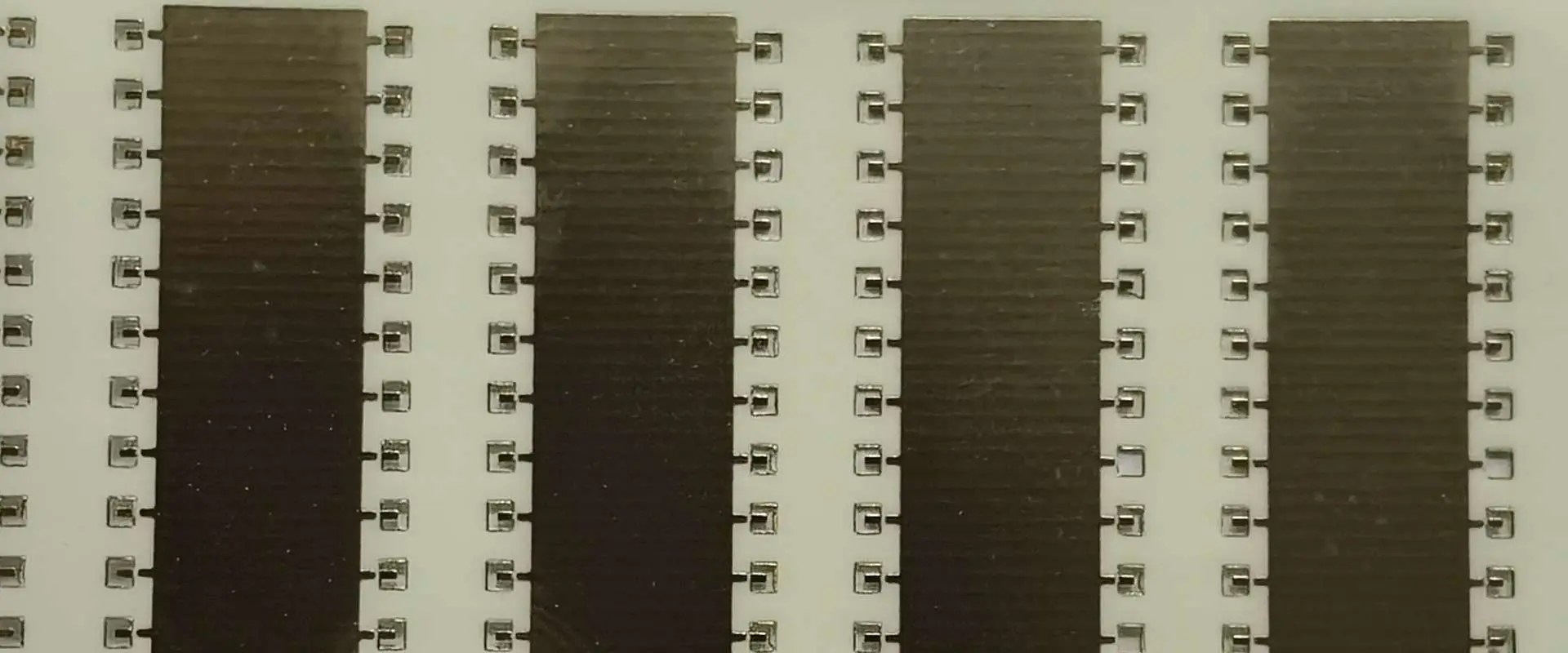
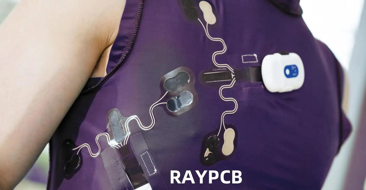
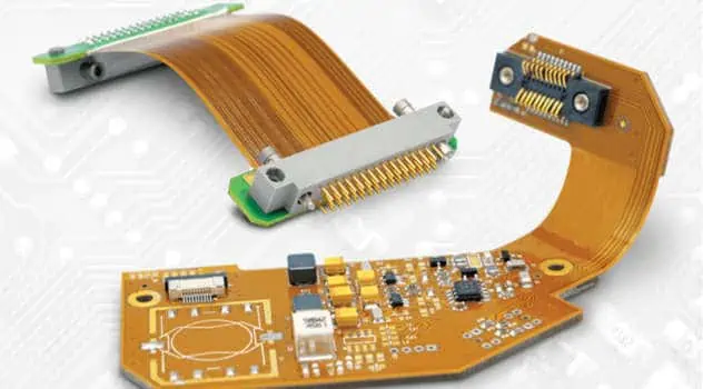
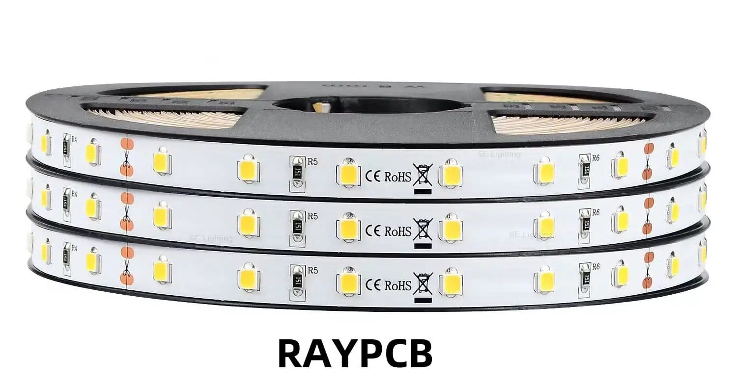
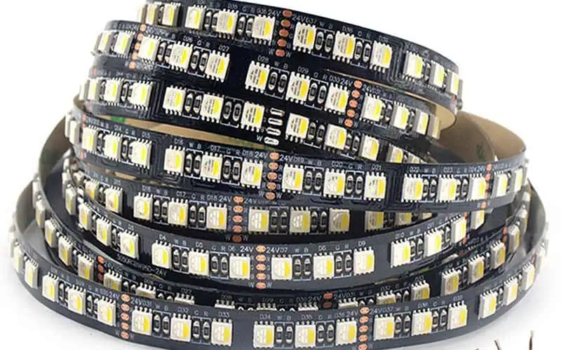
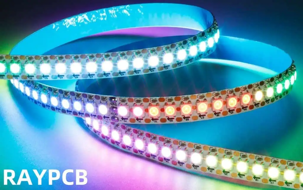
Flexible PCB LED strips are lighting products that consist of a series of LEDs mounted on a flexible printed circuit board. These strips can be bent, twisted, and conform to various shapes, making them ideal for applications where traditional rigid PCBs would be impractical.
Key Components of Flexible PCB LED Strips
- Flexible PCB: The base material that provides electrical connections and mechanical support.
- LEDs: Light-emitting diodes that produce the actual illumination.
- Resistors: Components that control current flow to the LEDs.
- Connectors: Allow for easy connection to power sources and other strips.
- Adhesive Backing: Enables easy mounting on various surfaces.
- Protective Coating: Provides water resistance and durability.
Design Considerations for Flexible PCB LED Strips
Electrical Design
- LED Selection: Choose appropriate LEDs based on desired color, brightness, and power consumption.
- Circuit Layout: Design the circuit to ensure even current distribution and minimize voltage drop.
- Power Management: Calculate power requirements and incorporate necessary components for efficient operation.
Mechanical Design
- Flexibility: Determine the required bending radius and design accordingly.
- Thickness: Balance flexibility with durability when choosing PCB thickness.
- Length and Width: Consider standard sizes and customization options.
- Mounting Options: Design for various installation methods (adhesive backing, mounting clips, etc.).
Thermal Management
- Heat Dissipation: Incorporate thermal management solutions to prolong LED lifespan.
- Material Selection: Choose PCB materials with good thermal conductivity.
Environmental Considerations
- IP Rating: Design for appropriate ingress protection based on intended use.
- UV Resistance: Select materials that can withstand exposure to sunlight if used outdoors.
- Chemical Resistance: Consider potential exposure to cleaning agents or other chemicals.
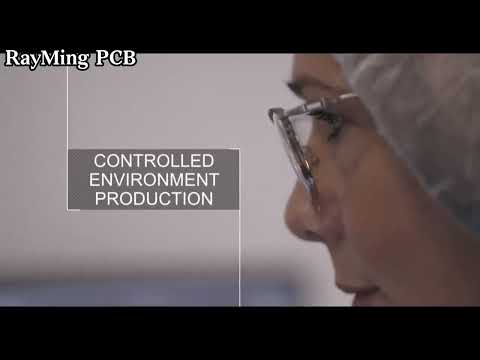
Manufacturing Process
Step 1: PCB Fabrication
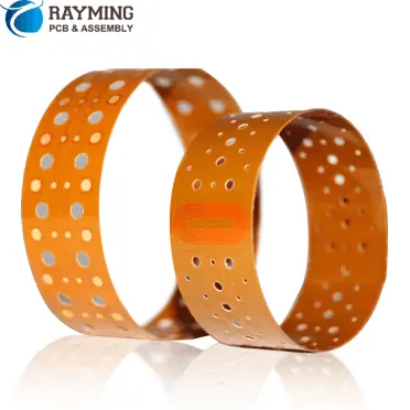
- Material Selection: Choose appropriate flexible PCB materials (e.g., polyimide, PET).
- Copper Layering: Apply copper foil to the flexible substrate.
- Photolithography: Create the circuit pattern using photoresist and etching processes.
- Surface Finish: Apply surface treatments (e.g., ENIG, HASL) to protect copper traces.
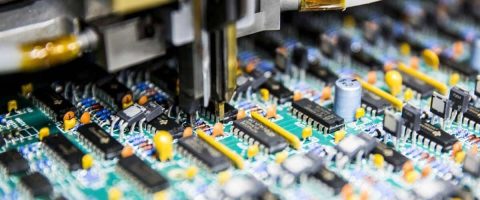
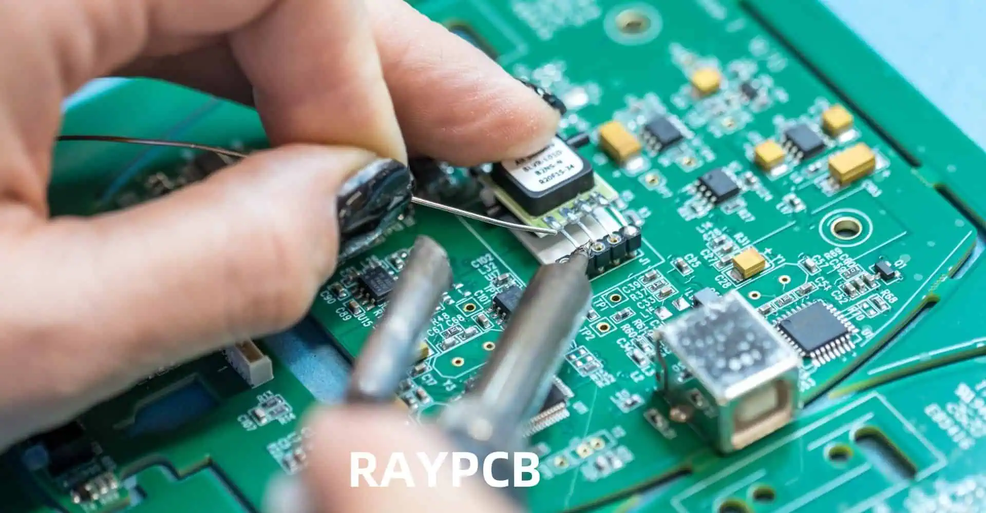
Step 2: Component Assembly
- Solder Paste Application: Apply solder paste to the PCB using a stencil.
- Component Placement: Use pick-and-place machines to position LEDs and other components.
- Reflow Soldering: Heat the PCB to melt the solder and secure components.
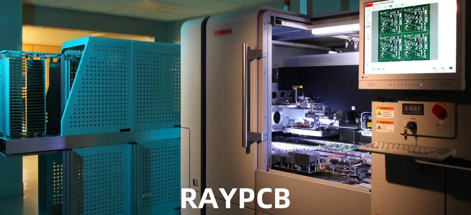
- Inspection: Perform automated optical inspection (AOI) to ensure proper assembly.
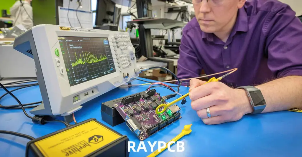
Step 3: Testing and Quality Control
- Electrical Testing: Verify continuity and proper functionality of the LED strips.
- Brightness and Color Testing: Ensure consistent light output and color accuracy.
- Flexibility Testing: Confirm that the strips can bend to the specified radius without damage.
- Environmental Testing: Subject samples to temperature, humidity, and other relevant tests.
Step 4: Finishing and Packaging
- Conformal Coating: Apply a protective layer to enhance durability and water resistance.
- Cutting and Termination: Cut strips to desired lengths and add end connectors.
- Adhesive Application: Apply double-sided adhesive tape to the back of the strips.
- Packaging: Package the LED strips in protective materials for shipping.
Overcoming Common Challenges

1. Maintaining Flexibility
Challenge: Ensuring the PCB remains flexible while accommodating necessary components and traces.
Solution:
- Use ultra-thin PCB materials (e.g., 0.1mm polyimide)
- Implement careful trace routing to avoid areas of high stress
- Utilize flexible solder masks and coverlays
2. Thermal Management
Challenge: Dissipating heat from densely packed LEDs on a flexible substrate.
Solution:
- Incorporate thermal vias to improve heat transfer
- Use thermally conductive adhesives for better heat dissipation
- Design with adequate spacing between high-power LEDs
3. Voltage Drop
Challenge: Maintaining consistent brightness along long LED strips due to voltage drop.
Solution:
- Implement parallel circuit designs to reduce voltage drop
- Use higher voltage power supplies (e.g., 24V instead of 12V)
- Incorporate voltage regulators or constant current drivers
4. Water and Dust Resistance
Challenge: Protecting the LED strips from environmental factors without compromising flexibility.
Solution:
- Apply conformal coatings that remain flexible when cured
- Design custom silicone or polyurethane encapsulations
- Use IP-rated connectors and sealing techniques at termination points
Comparison of Flexible PCB Materials for LED Strips
| Material | Flexibility | Temperature Resistance | Cost | Durability |
|---|---|---|---|---|
| Polyimide | Excellent | High (up to 200°C) | High | Excellent |
| PET | Good | Moderate (up to 105°C) | Low | Good |
| PEN | Very Good | Good (up to 150°C) | Moderate | Very Good |
| PTFE | Excellent | Very High (up to 260°C) | Very High | Excellent |
| FPC | Good | Moderate (up to 105°C) | Moderate | Good |
Design Optimization Techniques
1. Simulation and Modeling
Utilize advanced simulation software to model:
- Electrical performance
- Thermal behavior
- Mechanical stress
This helps identify potential issues before physical prototyping.
2. Modular Design
Implement a modular approach to:
- Facilitate easier customization
- Simplify manufacturing and inventory management
- Enable quick repairs and replacements
3. Smart Integration
Incorporate intelligent features such as:
- Built-in controllers for dynamic lighting effects
- Sensors for automatic brightness adjustment
- Wireless connectivity for remote control
4. Material Innovation
Explore cutting-edge materials:
- Stretchable conductive inks
- Novel flexible substrates with enhanced properties
- Advanced conformal coatings for improved protection
Future Trends in Flexible PCB LED Strip Design
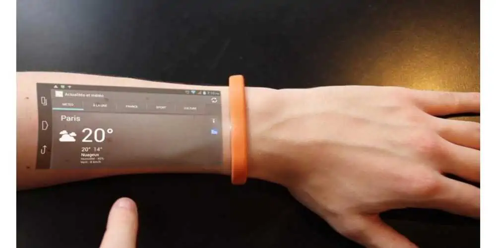
- Increased Integration: Combining LED strips with other flexible electronics (e.g., sensors, batteries).
- Enhanced Durability: Development of ultra-durable flexible PCBs for extreme environments.
- Improved Efficiency: Adoption of micro-LED technology for higher luminous efficacy.
- Sustainable Materials: Increased use of eco-friendly and recyclable materials in production.
- Customization: Advanced manufacturing techniques allowing for more complex and customized designs.
Conclusion
Turning a flexible PCB LED strip design into reality requires careful consideration of various factors, from electrical and mechanical design to manufacturing processes and quality control. By understanding these elements and implementing innovative solutions, designers and manufacturers can create high-quality, versatile lighting products that meet the diverse needs of modern applications. As technology continues to advance, we can expect even more exciting developments in the field of flexible PCB LED strips, pushing the boundaries of what’s possible in lighting design and functionality.
Frequently Asked Questions (FAQ)
1. What is the typical lifespan of a flexible PCB LED strip?
The lifespan of a flexible PCB LED strip can vary depending on several factors, including the quality of components, operating conditions, and usage patterns. On average, a well-designed and properly maintained LED strip can last between 30,000 to 50,000 hours of operation. This translates to approximately 3 to 6 years of continuous use. However, it’s important to note that factors such as heat management, voltage stability, and environmental protection can significantly impact the actual lifespan.
2. Can flexible PCB LED strips be cut to custom lengths?
Yes, most flexible PCB LED strips are designed to be cut to custom lengths. They typically have designated cutting points marked along the strip, usually every few LEDs. These cutting points are designed to ensure that the circuit remains intact after cutting. However, it’s crucial to cut only at these designated points to avoid damaging the strip or creating short circuits. After cutting, you may need to apply a sealant or use end caps to protect the exposed end of the strip, especially for outdoor or moisture-prone applications.
3. How do I choose the right power supply for my flexible PCB LED strip?
Selecting the right power supply is crucial for the proper operation and longevity of your LED strip. Consider the following factors:
- Voltage: Ensure the power supply matches the LED strip’s required voltage (typically 12V or 24V).
- Wattage: Calculate the total power consumption of your LED strip and choose a power supply with at least 20% higher capacity to account for power loss and future expansion.
- Quality: Opt for a high-quality, stable power supply to prevent flickering and ensure consistent performance.
- Safety Certifications: Look for power supplies with relevant safety certifications (e.g., UL, CE) for your region.
As a general rule, it’s better to slightly oversize your power supply to ensure stable operation and allow for potential expansion of your lighting setup.
4. Are there any special considerations for outdoor use of flexible PCB LED strips?
When using flexible PCB LED strips outdoors, consider the following:
- IP Rating: Choose strips with an appropriate Ingress Protection (IP) rating for water and dust resistance. IP65 or higher is typically recommended for outdoor use.
- UV Resistance: Ensure the strip and its components are designed to withstand prolonged exposure to sunlight.
- Temperature Range: Verify that the strip can operate within the expected temperature range of your outdoor environment.
- Proper Installation: Use weatherproof housings or channels to provide additional protection.
- Sealed Connections: Employ waterproof connectors and sealants at all connection points.
- Ventilation: Despite being outdoors, ensure proper ventilation to prevent overheating, especially in enclosed fixtures.
5. How can I ensure color consistency across multiple flexible PCB LED strips?
Maintaining color consistency across multiple LED strips can be challenging but is crucial for many applications. Here are some strategies:
- Binning: Purchase LED strips from the same production batch or “bin” to ensure similar color characteristics.
- Color Temperature Control: Use strips with precise color temperature specifications and consider incorporating tunable white technology for adjustability.
- Quality Control: Implement strict quality control measures during manufacturing and perform color testing before installation.
- Calibration: Use RGB or RGBW strips with built-in or external controllers that allow for individual color channel adjustments.
- Consistent Power Supply: Ensure all strips receive stable and consistent power to prevent voltage-related color shifts.
- Regular Maintenance: Periodically check and adjust color settings, as LEDs may change slightly over time.
By addressing these factors, you can significantly improve color consistency across your flexible PCB LED strip installation.