What is Image Transfer in PCB Manufacturing?

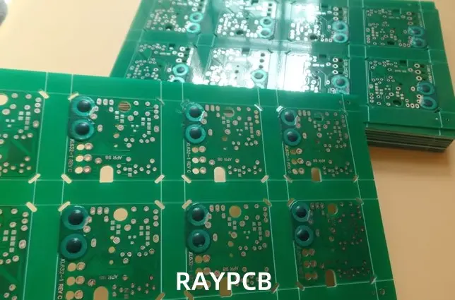
Image transfer in PCB (Printed Circuit Board) manufacturing is a crucial step that determines the quality and accuracy of the final circuit board. This process involves transferring the circuit design pattern onto the copper-clad board, which serves as the foundation for subsequent manufacturing steps. Understanding this process is essential for anyone involved in PCB production, design, or quality control.

The Fundamentals of PCB Image Transfer

Basic Principles

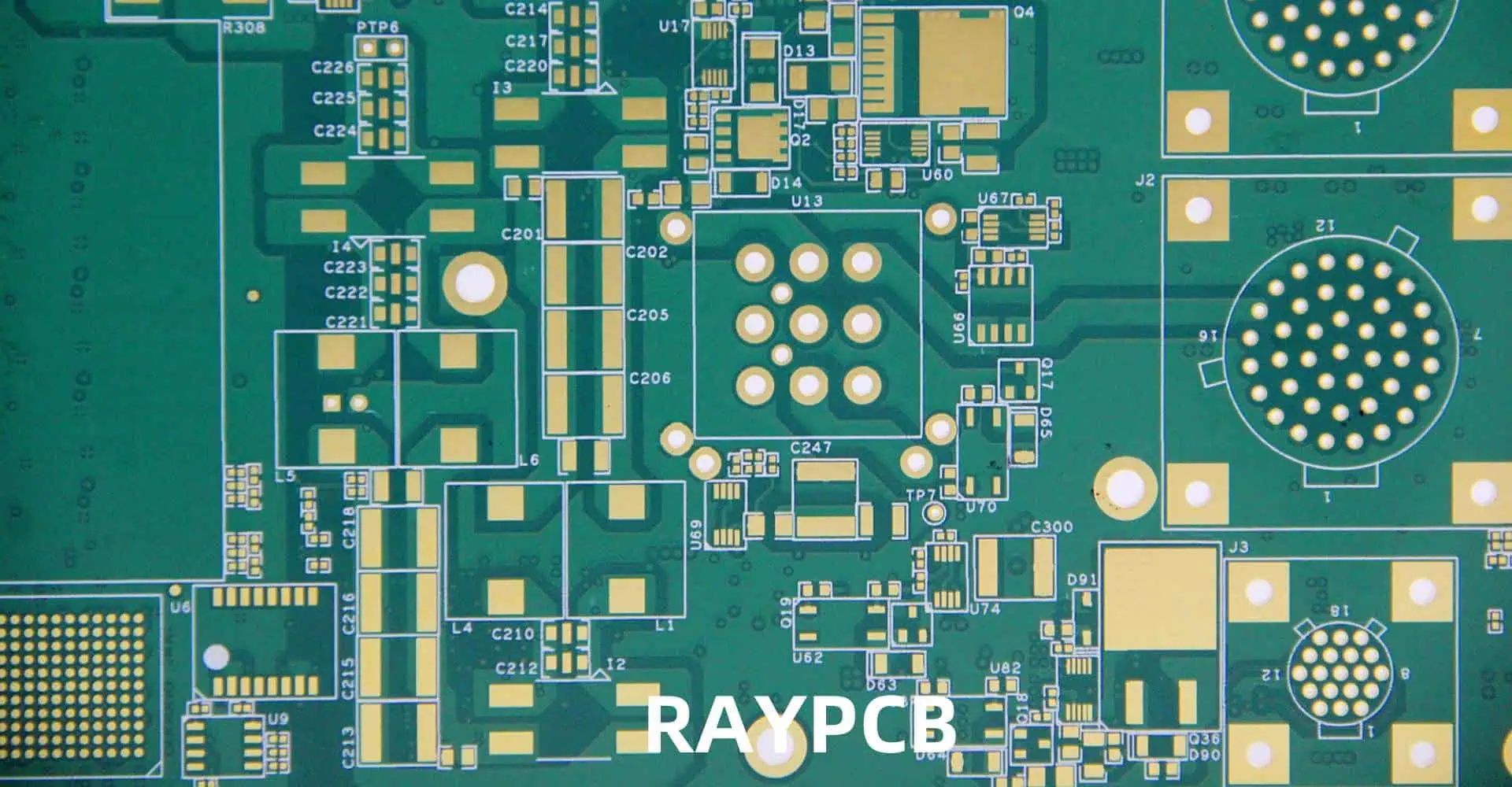
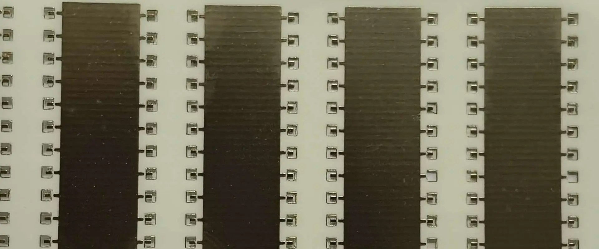
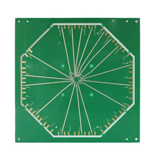
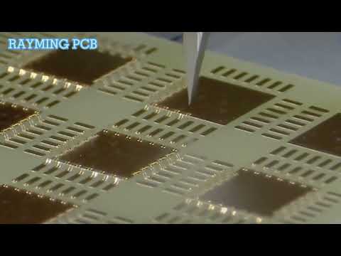
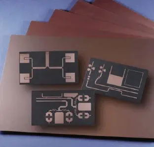
Image transfer in PCB manufacturing refers to the process of accurately reproducing the circuit design onto the copper surface of the board. This process is fundamental to creating the conductive pathways that will eventually form the functional circuit. The transfer must be precise, as even minor imperfections can lead to circuit failures or reliability issues.

Types of Image Transfer Methods

1. Photolithography

Toner Transfer
Toner Transfer

Photolithography remains the most widely used method in professional PCB manufacturing. This process involves:

  • Application of photoresist
  • Exposure to UV light
  • Development of the image
  • Etching of exposed copper
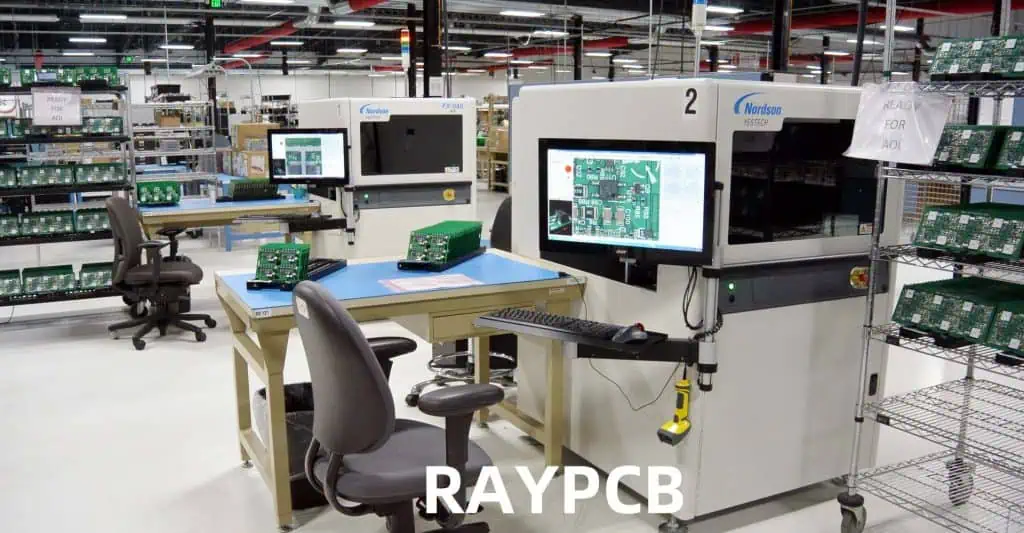
2. Direct Imaging

Direct imaging is a modern approach that eliminates the need for phototools. Benefits include:

  • Higher accuracy
  • Reduced environmental impact
  • Faster turnaround time
  • Better fine-line capability

3. Screen Printing

Screen printing is often used for:

  • Prototype development
  • Small-scale production
  • Specific applications requiring thick conductor deposits

Materials and Equipment

Essential Materials

Material Purpose Key Characteristics
Photoresist Image formation UV-sensitive, chemical resistant
Developer solution Pattern development Specific to resist type
Cleaning solutions Surface preparation Non-residue forming
Protective films Layer protection Clear, uniform thickness

Required Equipment

Equipment Type Function Precision Level
UV exposure unit Pattern exposure ยฑ10 microns
Direct imaging system Digital pattern transfer ยฑ5 microns
Screen printer Manual pattern transfer ยฑ25 microns
Clean room facilities Environmental control Class 100-1000

The Image Transfer Process

Step 1: Surface Preparation

Before image transfer can begin, the copper surface must be properly prepared:

  1. Cleaning and degreasing
  2. Mechanical or chemical roughening
  3. Anti-oxidation treatment
  4. Quality inspection

Step 2: Resist Application

The application of photoresist is critical and can be done through:

Method Advantages Disadvantages
Liquid resist coating Cost-effective, flexible Thickness variation
Dry film lamination Uniform thickness, clean Higher material cost
Electrophoretic coating Excellent coverage Complex process

Step 3: Exposure

Exposure Methods

Method Resolution Cost Production Speed
Contact printing Good Low Medium
Projection printing Better Medium High
Direct imaging Best High Very high

Step 4: Development

The development process reveals the circuit pattern:

  1. Chemical development
  2. Mechanical development
  3. Quality control inspection
  4. Pattern verification

Quality Control in Image Transfer

Critical Parameters

Parameter Acceptable Range Impact on Quality
Line width ยฑ10% of nominal Circuit performance
Registration ยฑ0.075mm Layer alignment
Edge definition 90ยฐ ยฑ5ยฐ Signal integrity
Surface roughness Ra โ‰ค 0.5ฮผm Adhesion quality

Common Defects

Visual Defects

  1. Under-exposure
  2. Over-exposure
  3. Poor adhesion
  4. Incomplete development

Electrical Defects

  1. Short circuits
  2. Open circuits
  3. Incorrect impedance
  4. Poor conductivity

Advanced Technologies

Latest Developments

  1. LED-based direct imaging
  2. Laser direct imaging (LDI)
  3. Inkjet printing technology
  4. Digital light processing (DLP)

Future Trends

Technology Expected Impact Timeline
AI-powered imaging Enhanced accuracy 2024-2025
Nano-resolution Finer features 2025-2026
Green processes Reduced waste 2023-2024
Smart automation Higher efficiency 2024-2025

Environmental Considerations

Waste Management

  1. Chemical disposal
  2. Water treatment
  3. Air filtration
  4. Material recycling

Sustainable Practices

Practice Environmental Benefit Implementation Cost
Water recycling 40% reduction in usage Medium
Energy efficiency 30% power savings High
Green chemistry 50% less toxic waste Medium
Material recovery 25% material savings Low

Cost Analysis

Cost Factors

Factor Percentage of Total Cost Control Methods
Materials 35-40% Bulk purchasing
Equipment 25-30% Preventive maintenance
Labor 20-25% Training and automation
Utilities 10-15% Energy efficiency

Frequently Asked Questions (FAQ)

Q1: What is the minimum line width achievable with modern image transfer methods?

A: Modern direct imaging systems can achieve line widths as small as 25 microns (0.001 inches) with high reliability. However, standard production typically works with 75-100 micron lines for better yield and cost-effectiveness.

Q2: How long does the image transfer process typically take?

A: The complete image transfer process, including preparation and quality control, typically takes 30-60 minutes per board. However, this can vary significantly based on:

  • Board complexity
  • Production volume
  • Equipment capability
  • Quality requirements

Q3: What are the main factors affecting image transfer quality?

A: The main factors include:

  • Material cleanliness
  • Environmental conditions
  • Equipment calibration
  • Operator skill
  • Process parameters

Q4: How often should image transfer equipment be calibrated?

A: Professional equipment should be calibrated:

  • Daily for basic parameters
  • Weekly for comprehensive checks
  • Monthly for full system calibration
  • Annually for certified calibration

Q5: What are the advantages of direct imaging over traditional photolithography?

A: Direct imaging offers several advantages:

  • Higher accuracy and resolution
  • Faster turnaround time
  • No need for phototools
  • Better environmental profile
  • Reduced material waste

Conclusion

Image transfer in PCB manufacturing is a complex process that requires careful attention to detail, proper equipment, and skilled operators. As technology advances, new methods and improvements continue to emerge, making the process more efficient and environmentally friendly. Understanding and optimizing this crucial step in PCB manufacturing is essential for producing high-quality prototype circuit boards assembly that meet modern electronic requirements.


Quick Turn and Fast PCB Prototype for Engineers and Makers

In today’s fast-paced electronics development environment, quick-turn PCB prototyping has become essential for engineers and makers. This comprehensive guide explores the various aspects of rapid PCB prototyping, from design considerations to manufacturing processes and quality control.

Understanding Quick-Turn PCB Services

Standard Turnaround Times

Service Level Production Time Transit Time Total Time Price Premium
Standard 4-5 days 2-3 days 6-8 days Base Price
Expedited 2-3 days 1-2 days 3-5 days 50%
Super Rush 24 hours 1 day 2 days 100%
Same Day 8-12 hours Same day 1 day 200%

Layer Count Options

Layer Count Typical Turn Time Complexity Level Common Applications
1-2 layers 24-48 hours Basic Simple prototypes
4 layers 2-3 days Moderate General electronics
6 layers 3-4 days Intermediate Complex circuits
8+ layers 4-5 days Advanced High-density designs

Design Considerations for Fast Turnaround

PCB Specifications

Parameter Standard Range Express Range Impact on Time
Min Trace Width 4-6 mil 6-8 mil Significant
Min Spacing 4-6 mil 6-8 mil Significant
Min Hole Size 0.2-0.3mm 0.3-0.4mm Moderate
Aspect Ratio Up to 10:1 Up to 8:1 Moderate

Material Selection Guide

Material Type Processing Time Cost Impact Applications
FR-4 Fastest Base cost General use
High Tg FR-4 +1 day 20% Industrial
Rogers +2-3 days 200% RF/Microwave
Flex +2-3 days 150% Flexible circuits

Manufacturing Process Optimization

File Preparation Requirements

File Type Format Critical Elements Time Saving
Gerber RS-274X Layer alignment Essential
Drill Excellon Tool definitions Essential
BOM Excel/CSV Component specs Optional
Assembly PDF/ODB++ Position data Optional

Quality Control Levels

QC Level Time Added Cost Added Recommended Use
Basic None Included Simple boards
Standard +2 hours 10% General projects
Advanced +4 hours 25% Critical projects
Full +8 hours 40% High-reliability

Special Features and Time Impact

Surface Finish Options

Finish Type Processing Time Durability Cost Impact
HASL Base time Standard Base cost
ENIG +1 day High 40%
Immersion Tin +1 day Moderate 30%
Hard Gold +2 days Very High 100%

Special Requirements

Feature Time Impact Cost Impact Application
Controlled Impedance +1 day 30% RF designs
Blind/Buried Vias +2 days 50% HDI designs
Heavy Copper +1 day 40% Power circuits
Via-in-pad +1 day 35% BGA designs

Cost Optimization Strategies

Volume vs. Time Trade-offs

Quantity Time Impact Cost per Board Notes
1-5 pcs Base time 100% Fastest option
6-20 pcs +1 day -30% Good balance
21-50 pcs +2 days -50% Economic choice
50+ pcs +3-4 days -65% Best value

Panel Optimization

Panel Size Board Quantity Cost Efficiency
50x50mm 1-4 boards Base cost
100x100mm 4-16 boards -20%
150x150mm 9-36 boards -35%
200x200mm 16-64 boards -50%

Project Management Tips

Documentation Checklist

Document Type Purpose Time Saving
Design Files Manufacturing Essential
Assembly Notes Build guidance Important
Test Specifications Quality control Optional
Component List Procurement Important

Common Time-Saving Practices

Practice Time Saved Implementation Effort
Design Templates 2-4 hours One-time setup
Library Management 1-2 hours Ongoing
DFM Guidelines 2-3 hours Per project
Pre-flight Checks 1 hour Per submission

Testing and Validation

Test Methods

Method Time Required Coverage Cost
Flying Probe 1-2 hours 98% Moderate
AOI 30 minutes 95% Low
Manual Check 1 hour 90% Low
X-ray 2 hours 100% High

Quality Metrics

Metric Target Range Impact on Time
First Pass Yield >95% Critical
Registration ยฑ3 mil Moderate
Soldermask ยฑ2 mil Low
Hole Tolerance ยฑ3 mil Moderate

Frequently Asked Questions

Q1: What is the fastest possible turnaround time for a standard 2-layer PCB prototype?

A1: For a standard 2-layer PCB, the fastest turnaround time is typically 24 hours for manufacturing plus shipping time. This assumes standard FR-4 material, HASL finish, and no special requirements. However, this comes with a significant price premium, usually 2-3 times the standard price.

Q2: How do special requirements affect the quick-turn timeline?

A2: Special requirements like controlled impedance, blind/buried vias, or special materials can add 1-3 days to the manufacturing time. It’s important to consider these requirements early in the design phase and communicate them clearly to the manufacturer.

Q3: What are the key factors that can help reduce prototype turnaround time?

A3: Key factors include: providing complete and accurate design files, choosing standard materials and processes, avoiding special requirements when possible, and using the manufacturer’s preferred file formats. Pre-validation of design files can also significantly reduce potential delays.

Q4: How does board complexity affect quick-turn pricing and timeline?

A4: Board complexity, including layer count, feature size, and special requirements, directly impacts both price and timeline. Higher complexity generally means longer production time and higher costs. A 4-layer board typically takes 1-2 days longer than a 2-layer board.

Q5: What are the trade-offs between speed and cost in PCB prototyping?

A5: Faster turnaround times typically come with significant price premiums. Super rush services (24-48 hours) can cost 2-3 times more than standard services (5-7 days). Balancing speed against budget requires careful consideration of project requirements and deadlines.

Conclusion

Quick-turn PCB prototyping services provide essential support for rapid product development and innovation. Success in fast-turn PCB prototyping requires careful planning, clear communication, and understanding of the trade-offs between speed, cost, and quality. By following the guidelines and best practices outlined in this article, engineers and makers can optimize their prototype development process and achieve better results in shorter timeframes.

Difference between Chemical and Plasma Etch Processes

Etching processes play a crucial role in semiconductor manufacturing and PCB production. Understanding the differences between chemical and plasma etching is essential for choosing the right process for specific applications. This comprehensive guide explores both methods, their characteristics, applications, and comparative advantages.

Basic Principles

Chemical Etching Fundamentals

ParameterDescriptionImpact
Process TypeWet chemical reactionMaterial selective removal
Main MechanismChemical dissolutionIsotropic etching pattern
Temperature Range20-50ยฐC typicallyAffects etch rate
EnvironmentLiquid phaseRequires chemical handling
Reaction TypeSpontaneousLess energy intensive

Plasma Etching Fundamentals

ParameterDescriptionImpact
Process TypeIon bombardment + chemicalDirectional material removal
Main MechanismPhysical-chemical reactionAnisotropic etching pattern
Temperature Range50-300ยฐC typicallyAffects selectivity
EnvironmentGas phaseVacuum required
Reaction TypeEnergy-activatedMore energy intensive

Process Characteristics

Chemical Etching Parameters

Control Factors

FactorControl RangeEffect on Process
Temperature20-50ยฐCEtch rate ยฑ20%
Concentration5-30%Etch rate ยฑ50%
Agitation0-500 rpmUniformity ยฑ15%
TimeMinutes to hoursLinear progression

Material Compatibility

MaterialEtchant TypeTypical Etch Rate
CopperFeCl31-3 ฮผm/min
AluminumNaOH0.5-2 ฮผmm/min
SiliconKOH0.5-1 ฮผm/min
GlassHF0.1-0.5 ฮผm/min

Plasma Etching Parameters

Process Variables

VariableControl RangeEffect on Process
Power100-2000WEtch rate ๅค30%
Pressure1-1000 mTorrDirectionality ๅค40%
Gas Flow10-200 sccmChemistry control
Bias Voltage0-1000VIon energy control

Gas Chemistry Options

Gas TypeTarget MaterialSelectivity
CF4SiliconHigh
O2OrganicsVery High
Cl2MetalsModerate
SF6SiliconModerate

Comparative Analysis

Performance Metrics

MetricChemical EtchingPlasma Etching
Resolution50-100 ๆธญm0.1-1 ๆธญm
Aspect Ratio1:1 to 3:1Up to 20:1
Uniformityยฑ10-15%ยฑ5-10%
ThroughputHighModerate
CostLowerHigher

Environmental Impact

FactorChemical EtchingPlasma Etching
Waste GenerationHigh liquid wasteLow gas waste
Chemical UsageHigh volumeLow volume
Energy ConsumptionLowerHigher
Environmental RiskHigherLower

Applications and Use Cases

Chemical Etching Applications

ApplicationAdvantagesLimitations
PCB ManufacturingCost-effectiveLimited resolution
Metal DecorationLarge area capableChemical handling
MEMS FabricationHigh throughputIsotropic only
Photo Chemical MachiningComplex patternsMaterial constraints

Plasma Etching Applications

ApplicationAdvantagesLimitations
SemiconductorHigh precisionHigher cost
Advanced MEMSHigh aspect ratioLower throughput
Optical DevicesClean processComplex control
NanofabricationPrecise controlSize limitations

Process Selection Guidelines

Decision Matrix

RequirementRecommended ProcessReason
High Volume, Lower PrecisionChemicalCost-effective
High Precision, Small FeaturesPlasmaBetter control
Large Area ProcessingChemicalBetter throughput
Complex 3D StructuresPlasmaDirectional control

Cost Considerations

Cost FactorChemical EtchingPlasma Etching
Equipment$10K-100K$100K-1M
Operating Cost$50-200/hour$200-1000/hour
MaintenanceMonthlyQuarterly
TrainingBasicAdvanced

Process Optimization

Chemical Etch Optimization

Control Strategies

ParameterOptimization MethodExpected Impact
TemperaturePID controlยฑ2ยฐC stability
ConcentrationRegular monitoringยฑ5% variation
AgitationSpeed controlUniform exposure
Bath LifeChemical analysisConsistent results

Plasma Etch Optimization

Process Control

ParameterOptimization MethodExpected Impact
PowerRF matchingStable plasma
PressureAutomated controlConsistent process
Gas FlowMass flow controlRepeatable results
Chamber CleanRegular maintenanceProcess stability

Safety Considerations

Chemical Etching Safety

AspectRequirementImplementation
Ventilation6-12 air changes/hourFume hoods
PPEChemical resistantGloves, goggles, apron
Waste HandlingNeutralizationTreatment system
Emergency ResponseSpill controlSafety showers

Plasma Etching Safety

AspectRequirementImplementation
High VoltageInterlocksSafety systems
VacuumPressure monitoringAutomated control
Gas SafetyGas detectionMonitoring systems
RF RadiationShieldingEnclosed systems

Future Trends

Technology Development

AreaChemical EtchingPlasma Etching
AutomationBath monitoringFull process control
ResolutionImproved chemistryAdvanced power control
EnvironmentalRecycling systemsEnergy efficiency
IntegrationInline processingCluster tools

Frequently Asked Questions

Q1: What are the main factors determining the choice between chemical and plasma etching?

A1: The main factors include feature size requirements, aspect ratio needs, material type, production volume, and cost constraints. Chemical etching is typically chosen for larger features and higher volumes, while plasma etching is preferred for precise, small features and complex structures.

Q2: How do the operational costs compare between chemical and plasma etching?

A2: Chemical etching generally has lower operational costs due to simpler equipment and processes, but higher chemical disposal costs. Plasma etching has higher equipment and energy costs but lower material and waste management costs.

Q3: What are the environmental implications of both processes?

A3: Chemical etching generates more liquid waste requiring treatment and disposal, while plasma etching has higher energy consumption but produces less waste. Plasma etching is generally considered more environmentally friendly despite higher energy usage.

Q4: Can these processes be combined for better results?

A4: Yes, some applications use a combination of both processes, where chemical etching is used for bulk material removal followed by plasma etching for fine feature definition and surface finishing.

Q5: What are the typical maintenance requirements for each process?

A5: Chemical etching requires frequent bath monitoring and replacement, typically monthly maintenance. Plasma etching systems need less frequent but more specialized maintenance, usually quarterly, including chamber cleaning and RF system checks.

Conclusion

The choice between chemical and plasma etching depends on specific application requirements, including precision, throughput, cost, and environmental considerations. While chemical etching offers cost-effective solutions for larger features and higher volumes, plasma etching provides superior control and precision for advanced applications. Understanding these differences enables proper process selection and optimization for specific manufacturing needs.

Prototyping Your PCBs: Europe vs China – A Comprehensive Guide

40 Layer PCB

When developing electronic products, one of the most critical decisions engineers and product developers face is where to manufacture their printed circuit board (PCB) prototypes. The choice between European and Chinese manufacturers can significantly impact project timelines, costs, quality, and overall development experience. This comprehensive analysis explores the key factors to consider when deciding between these two major manufacturing regions.

Cost Considerations: The Bottom Line Impact

The most apparent difference between European and Chinese PCB prototyping lies in pricing. Chinese manufacturers typically offer significantly lower costs, often 30-70% less expensive than their European counterparts. This cost advantage stems from several factors including lower labor costs, economies of scale, and government subsidies supporting the electronics manufacturing sector.

Chinese PCB houses have invested heavily in automation and high-volume production capabilities, allowing them to spread fixed costs across larger production runs. Even for prototypes, this infrastructure advantage translates to competitive pricing. A typical 4-layer prototype PCB that might cost โ‚ฌ50-80 from a European supplier could be produced in China for โ‚ฌ15-30, including shipping.

However, European manufacturers often provide better value propositions when considering total project costs. Their proximity reduces shipping expenses and eliminates import duties, while faster turnaround times can accelerate development cycles, potentially saving weeks of engineering time worth thousands of euros. For time-sensitive projects or when multiple prototype iterations are required, the higher upfront cost of European manufacturing may prove more economical overall.

Quality and Manufacturing Standards

Both regions are capable of producing high-quality PCBs, but their approaches and certifications differ significantly. European manufacturers typically adhere to stricter environmental and quality standards from the outset. They commonly maintain certifications such as ISO 9001, ISO 14001, and IPC standards as baseline requirements rather than premium offerings.

Chinese manufacturers have made remarkable improvements in quality over the past decade. Leading Chinese PCB houses now rival their Western counterparts in technical capabilities and quality control. However, quality can vary significantly between manufacturers, making vendor selection more critical. Top-tier Chinese facilities often exceed European quality standards, while lower-tier suppliers may struggle with consistency.

European manufacturers generally provide more comprehensive quality documentation and traceability. Their quality management systems are often more transparent, with detailed process documentation and easier access to quality managers for discussions about specific requirements. This transparency can be crucial for projects requiring extensive documentation or compliance with strict regulatory requirements.

The manufacturing processes also differ in their approach to quality control. European facilities typically implement more conservative design rules and manufacturing parameters, resulting in higher yields but potentially limiting the ability to push technological boundaries. Chinese manufacturers are often more willing to attempt aggressive design specifications, though this may come with higher risk of manufacturing defects.

Turnaround Times and Logistics

Turnaround time represents one of the most significant differences between regional choices. European PCB manufacturers typically offer 3-10 business days for standard prototypes, with some specializing in same-day or next-day service for premium pricing. This rapid turnaround enables faster design iteration cycles and can significantly accelerate product development timelines.

Chinese manufacturers usually require 7-15 business days for production, plus 3-7 days for international shipping. However, some Chinese suppliers now offer expedited services with 3-5 day production times, though at premium pricing that may approach European cost levels. The total time from order to receipt typically ranges from 10-22 business days when using Chinese suppliers.

Shipping logistics add another layer of complexity when working with Chinese manufacturers. International shipping costs have fluctuated significantly in recent years, and customs delays can add unpredictable time to delivery schedules. European suppliers benefit from streamlined intra-EU shipping, with predictable delivery times and no customs complications for EU-based customers.

The reliability of delivery commitments also varies between regions. European manufacturers typically provide more accurate delivery estimates and have fewer external factors affecting their ability to meet promised dates. Chinese suppliers may face delays due to national holidays, shipping disruptions, or regulatory changes that can impact project timelines unexpectedly.

Technical Capabilities and Specialization

Both European and Chinese manufacturers offer sophisticated technical capabilities, but their specializations often differ. Chinese manufacturers excel in high-volume production techniques and have invested heavily in advanced equipment for cutting-edge technologies. Many Chinese facilities operate the latest generation of manufacturing equipment and can handle extremely complex designs with fine pitch components and advanced materials.

European manufacturers often specialize in niche applications and custom solutions. They typically provide superior engineering support and are more willing to work on unusual or challenging designs that require extensive collaboration. European suppliers often maintain closer relationships with their customers, offering design advice and optimization suggestions that can improve product performance or manufacturability.

The range of materials and substrate options varies between regions. Chinese manufacturers typically stock a broader range of standard materials and can often accommodate special material requests more quickly due to their larger supplier networks. European manufacturers may have limited material options but often provide superior material traceability and certification documentation.

Advanced technologies such as embedded components, flex-rigid designs, and high-frequency applications are available from both regions, though the approach differs. Chinese manufacturers often focus on cost-effective implementation of advanced technologies, while European suppliers emphasize reliability and performance optimization.

Communication and Support

Language barriers and time zone differences significantly impact the working relationship with Chinese suppliers. While many Chinese manufacturers employ English-speaking staff, technical discussions about complex requirements can still present challenges. Miscommunications about specifications or requirements can lead to incorrect prototypes and project delays.

European manufacturers offer the advantage of shared languages, similar business cultures, and overlapping working hours. This facilitates real-time communication during the design and manufacturing process, enabling quick resolution of questions or issues that arise during production.

The level of engineering support also differs between regions. European suppliers typically provide more comprehensive pre-production support, including design rule checking, manufacturability analysis, and optimization suggestions. Chinese manufacturers are improving in this area but may offer more limited engineering consultation, particularly for complex or unusual designs.

Customer service approaches reflect different business cultures. European suppliers often emphasize relationship building and long-term partnerships, providing personalized service and dedicated account management. Chinese manufacturers may focus more on efficient order processing and standardized service levels, though leading suppliers are increasingly investing in improved customer service capabilities.

Making the Decision: Key Factors to Consider

The choice between European and Chinese PCB prototyping should consider several project-specific factors. For early-stage prototypes where cost is the primary concern and timeline flexibility exists, Chinese manufacturers often provide the best value. Their ability to produce complex designs at low costs makes them attractive for projects with tight budget constraints.

Time-sensitive projects or those requiring multiple design iterations benefit from European suppliers’ faster turnaround times and easier communication. The ability to quickly discuss design changes or manufacturing questions can significantly accelerate development cycles, particularly for complex or innovative designs.

Regulatory requirements and documentation needs may favor European suppliers, particularly for medical devices, automotive applications, or other highly regulated industries. European manufacturers’ familiarity with EU regulations and quality documentation practices can simplify compliance processes.

Project volume and future production plans should also influence the decision. If prototypes will eventually transition to high-volume production, establishing relationships with Chinese manufacturers during the prototype phase may provide advantages for future manufacturing partnerships.

Conclusion

The decision between European and Chinese PCB prototyping involves balancing multiple factors including cost, quality, timeline, and project requirements. Chinese manufacturers excel in cost-effectiveness and technical capabilities, making them ideal for cost-sensitive projects with flexible timelines. European suppliers offer advantages in speed, communication, regulatory compliance, and engineering support, making them preferable for time-critical or highly regulated applications.

Rather than viewing this as an either-or decision, many successful companies develop relationships with suppliers in both regions, selecting the most appropriate option based on specific project needs. This hybrid approach provides flexibility while maximizing the advantages each region offers. Ultimately, the best choice depends on your specific project requirements, budget constraints, and development timeline priorities.

Have You Found Perfect China PCB Manufacturing House Service?

Rogers RT duroid 6006 PCB

Finding the ideal PCB manufacturing partner in China can be a game-changer for your electronics projects. With hundreds of manufacturers offering varying levels of service, quality, and pricing, making the right choice requires careful consideration of multiple factors. This comprehensive guide will help you navigate the Chinese PCB manufacturing landscape.

Understanding Chinese PCB Manufacturing Industry

Market Overview

CategoryNumber of ManufacturersMarket ShareQuality Level
Tier 120-3045%High-End
Tier 2100-15035%Mid-Range
Tier 3500+20%Entry-Level

Regional Distribution

RegionManufacturing ConcentrationSpecialization
ShenzhenVery HighConsumer Electronics
ShanghaiHighIndustrial PCBs
GuangzhouMediumAutomotive PCBs
SuzhouMediumMedical Electronics
DongguanHighPrototype Services

Key Criteria for Evaluation

Manufacturing Capabilities

Production Specifications

SpecificationStandard RangeAdvanced Range
Layer Count1.-1618-40+
Min Line Width4mil2mil
Min Spacing4mil2mil
Board Thickness0.4-3.2mm0.2-7.0mm
Aspect Ratio8:0120:01

Quality Certifications

CertificationImportanceIndustry Focus
ISO 9001EssentialGeneral Quality
ISO 14001ImportantEnvironmental
ULCriticalSafety Standards
IPC ClassNecessaryManufacturing
IATF 16949SpecificAutomotive

Top Chinese PCB Manufacturers Analysis

Comprehensive Comparison

CriteriaManufacturer AManufacturer BManufacturer CManufacturer D
Min Order5 pcs1 pc10 pcs3 pcs
Lead Time24h-5 days48h-7 days3-10 days24h-3 days
Price Level$$$$$$$$
QualityHighVery HighMediumHigh
CommunicationExcellentGoodFairVery Good

Service Package Comparison

Standard Services

Service ElementTier 1Tier 2Tier 3
DFM CheckComprehensiveBasicLimited
Technical Support7.-24Business HoursEmail Only
File Format SupportAll MajorCommonLimited
Quality Testing100%SamplingBasic
DocumentationCompleteStandardMinimal

Production Capabilities

Technology Parameters

ParameterBasic ServiceAdvanced ServiceHigh-End Service
Min Hole Size0.3mm0.2mm0.1mm
Copper Weight0.5-2oz0.5-3oz0.5-12oz
Surface FinishHASL, ENIGENIG, IAgAll Available
SoldermaskGreenMultiple ColorsAny Color
SilkscreenWhiteMultiple ColorsAny Color

Material Options

Material TypeCost FactorApplication
FR41xStandard
High Tg FR41.3xIndustrial
Rogers5-10xRF/Microwave
Aluminum2-3xLED/Power
Flex3-4xFlexible Circuits

Quality Control Processes

pattern plating line 2
Pattern plating line 2

Inspection Methods

StageBasic LevelAdvanced LevelPremium Level
IncomingVisualAutomatedFull Testing
In-ProcessSamplingRegularContinuous
FinalStandardEnhanced100% Testing
PackagingBasicProtectedCustom

Testing Capabilities

Test TypeStandard ServicePremium Service
AOIYesYes
Flying ProbeSample100%
X-rayNoYes
ImpedanceOptionalYes
MicrosectionOn RequestRegular

Communication and Support

Service Hours and Response Time

Service TypeResponse TimeAvailable HoursLanguage Support
Email2-4 hours7.-24English/Chinese
Online ChatImmediateBusiness HoursEnglish/Chinese
PhoneImmediateBusiness HoursChinese Primary
Technical Support4-8 hoursBusiness HoursEnglish/Chinese

Cost Structure

Price Components

ComponentPercentageVariable Factors
Materials30-40%Type, Quality
Labor20-25%Complexity
Overhead15-20%Location
Testing10-15%Level Required
Profit10-20%Market Position

Volume Pricing Example

QuantityUnit PriceSetup FeeTotal Cost
5.-10$20 $50 $150-250
11-50$15 $50 $215-800
51-100$10 $50 $560-1050
101-500$8 $50 $858-4050

Shipping and Logistics

Delivery Options

MethodCost/kgDurationTracking
Air Express$30-403-5 daysFull
Air Freight$15-255-7 daysPartial
Sea Freight$5-1030-40 daysBasic
Express Small$40-502-3 daysFull

Tips for Success

Key Success Factors

  1. Clear Specifications
  2. Proper Communication
  3. Quality Verification
  4. Sample Testing
  5. Documentation Review

Common Pitfalls to Avoid

IssuePrevention MethodImpact Level
Language BarrierUse Technical TermsHigh
Quality IssuesClear SpecsVery High
Delivery DelaysBuffer TimeMedium
Cost OverrunsDetailed QuoteHigh
Communication GapsRegular UpdatesMedium

Future Developments

Industry Trends

TrendImplementationImpact
AutomationIncreasingLower Costs
Smart FactoryDevelopingBetter Quality
Green ProductionGrowingHigher Standards
AI IntegrationEarly StagesImproved Accuracy

Frequently Asked Questions (FAQ)

Q1: How do I verify the reliability of a Chinese PCB manufacturer?

A1: Look for established manufacturers with proper certifications (ISO 9001, UL, etc.), check their customer reviews, request samples, and verify their communication capabilities. It’s also important to assess their technical support and quality control processes.

Q2: What are the typical lead times for PCB manufacturing in China?

A2: Lead times vary by manufacturer and service level. Standard production typically takes 3-5 days, while express services can deliver in 24-48 hours. Complex boards or special requirements may require 7-15 days.

Q3: How can I ensure quality when working with Chinese manufacturers?

A3: Provide clear specifications, request detailed DFM reports, order prototype pcb assembly samples before mass production, specify quality requirements in your order, and choose manufacturers with comprehensive testing capabilities and quality certifications.

Q4: What’s the best way to handle communication with Chinese manufacturers?

A4: Work with manufacturers who have English-speaking technical support, use clear technical terms, provide detailed documentation, and maintain regular communication through established channels (email, online platforms, etc.).

Q5: How do I protect my intellectual property when working with Chinese manufacturers?

A5: Sign NDAs, work with reputable manufacturers who have clear IP protection policies, limit access to sensitive information, and consider splitting production across different manufacturers for critical components.

Where Can You Purchase Cheap PCB of Low Volume?

40 Layer PCB

The world of electronics prototyping and small-scale production has been revolutionized by the availability of affordable, low-volume printed circuit board (PCB) manufacturing services. Whether you’re a hobbyist working on a personal project, a startup developing your first product, or an engineer creating prototypes for testing, finding cost-effective PCB suppliers for small quantities is crucial for keeping your project budget under control.

Understanding Low-Volume PCB Manufacturing

Low-volume PCB manufacturing typically refers to orders ranging from single prototypes to a few hundred boards. This market segment has experienced tremendous growth due to the maker movement, increased accessibility of design tools, and the proliferation of IoT devices requiring custom circuit boards. Unlike high-volume manufacturing where economies of scale drive down per-unit costs, low-volume production focuses on flexibility, quick turnaround times, and reasonable pricing for small quantities.

The key challenges in low-volume PCB procurement include balancing cost with quality, managing longer lead times compared to off-the-shelf components, and finding suppliers who can accommodate small orders without prohibitive setup fees. Fortunately, numerous manufacturers now specialize in this market segment, offering competitive pricing and services tailored to small-scale needs.

Online PCB Manufacturing Services

The most accessible option for purchasing cheap, low-volume PCBs is through online manufacturing services. These platforms have streamlined the ordering process, often providing instant quotes and automated design rule checks.

JLCPCB stands out as one of the most popular choices for budget-conscious buyers. Based in China, they offer extremely competitive pricing, with basic two-layer boards starting as low as $2 for five pieces. Their online platform is user-friendly, supporting major CAD file formats, and they provide additional services like SMT assembly for complete board population. The main trade-offs are longer shipping times for international orders and limited customer service hours due to time zone differences.

PCBWay is another Chinese manufacturer offering competitive pricing and good quality control. They provide detailed manufacturing specifications, real-time order tracking, and support for complex board designs including flexible and rigid-flex PCBs. Their pricing is slightly higher than JLCPCB but often includes better packaging and quality assurance.

Seeed Studio Fusion combines PCB manufacturing with their broader ecosystem of development tools and components. They offer reasonable pricing for prototypes and small batches, with the added benefit of being able to source components and provide assembly services in one location. This integration can simplify the supply chain for complete project development.

For those preferring domestic suppliers, OSH Park in the United States offers high-quality PCBs with their distinctive purple solder mask. While more expensive than overseas options, they provide faster shipping, excellent customer service, and support for the maker community. Their pricing model is straightforward, charging per square inch of board area.

Traditional PCB Manufacturers

Many established PCB manufacturers have adapted their business models to accommodate low-volume orders. These companies often provide superior quality control and customer service compared to online-only services, though typically at higher prices.

Advanced Circuits is a US-based manufacturer offering their “33 each” service, providing 33 copies of a simple two-layer board for a fixed price. This can be extremely cost-effective for designs that fit their standard parameters. They also offer express services for rush orders and provide excellent technical support for design optimization.

Sunstone Circuits specializes in quick-turn prototypes and low-volume production. Their PCB123 software integrates design and ordering, streamlining the process from concept to finished board. While more expensive than overseas options, they offer rapid turnaround times and US-based manufacturing for projects requiring quick iterations.

Regional manufacturers often provide competitive pricing for local customers due to reduced shipping costs and faster communication. Researching local PCB shops can uncover hidden gems that offer personalized service and competitive pricing for small orders.

Factors Affecting PCB Cost

Understanding the factors that influence PCB pricing helps in making informed decisions and potentially reducing costs through design optimization. Board size is the most significant factor, as manufacturers typically charge based on panel utilization. Designing boards to fit standard panel sizes or using panelization for multiple small boards can reduce per-unit costs.

Layer count dramatically affects pricing, with four-layer boards typically costing 2-3 times more than two-layer boards. Unless high-speed signals or complex routing require additional layers, keeping designs to two layers significantly reduces costs. Via types also impact pricing, with buried and blind vias adding substantial cost compared to through-hole vias.

Surface finish selection affects both cost and performance. HASL (Hot Air Solder Leveling) is typically the cheapest option, while ENIG (Electroless Nickel Immersion Gold) costs more but provides better solderability and shelf life. For prototypes and low-cost applications, HASL usually provides adequate performance.

Solder mask and silkscreen colors can affect pricing, with green solder mask and white silkscreen being the most economical choices. Exotic colors or multiple silkscreen colors may incur additional charges.

Design Considerations for Cost Optimization

Optimizing PCB designs for manufacturing can significantly reduce costs without compromising functionality. Using standard trace widths and spacing helps avoid manufacturing surcharges for fine-pitch features. Most low-cost manufacturers have standard capabilities that accommodate typical design requirements without additional fees.

Minimizing drill sizes and types reduces manufacturing complexity and cost. Using standard via sizes and avoiding micro-vias keeps boards within standard manufacturing parameters. Similarly, maintaining adequate spacing between features ensures high yield rates and reduces the likelihood of manufacturing defects.

Component placement optimization can reduce board size, the primary cost driver. Efficient routing and component placement not only reduces material costs but can also improve electrical performance and reduce assembly complexity.

Quantity Considerations and Break Points

Understanding quantity break points helps optimize order sizes for best value. Many manufacturers offer significant price reductions at specific quantity thresholds, typically at 10, 25, 50, and 100 pieces. Sometimes ordering slightly more boards to reach the next price break results in lower per-unit costs.

For ongoing projects, consider future needs when placing orders. PCB shelf life is typically several years when properly stored, so ordering larger quantities during initial prototyping phases can reduce long-term costs if the design is stable.

Quality vs. Cost Trade-offs

While cost is important, quality cannot be ignored entirely. Cheap PCBs that fail during testing or have poor solderability can ultimately cost more than initially paying for higher-quality boards. Reading reviews, requesting samples, and starting with small orders helps evaluate manufacturer quality before committing to larger quantities.

Most reputable low-cost manufacturers provide adequate quality for prototyping and low-volume production. However, for critical applications or products requiring certifications, investing in higher-quality manufacturers may be necessary.

Conclusion

The landscape for purchasing cheap, low-volume PCBs has never been more favorable for small-scale developers and hobbyists. Online manufacturing services from companies like JLCPCB and PCBWay provide excellent value for basic designs, while traditional manufacturers offer premium services for applications requiring higher quality or faster turnaround times.

Success in low-volume PCB procurement requires balancing cost, quality, and delivery requirements while optimizing designs for manufacturing efficiency. By understanding the factors affecting PCB costs and leveraging the competitive landscape of modern PCB manufacturing, developers can obtain high-quality boards at reasonable prices for their projects.

The key is matching your specific requirements with the right supplier, whether that’s the rock-bottom pricing of overseas online services or the premium quality and service of domestic manufacturers. With careful planning and design optimization, obtaining affordable PCBs for low-volume applications is entirely achievable in today’s market.

Board Plating and Hole Plating: What’s the Difference

In the intricate world of printed circuit board (PCB) manufacturing, plating processes play a crucial role in ensuring electrical connectivity, mechanical stability, and overall board reliability. Two fundamental plating techniques that often cause confusion among engineers and manufacturers are board plating and hole plating. While both involve the electrochemical deposition of metal onto PCB surfaces, they serve distinct purposes and employ different methodologies. Understanding these differences is essential for anyone involved in PCB design, manufacturing, or quality control.

Understanding Board Plating

Board plating, also known as panel plating or surface plating, refers to the process of depositing a thin layer of metal across the entire surface of a PCB panel or individual board. This comprehensive coating covers both the copper traces and the substrate material, creating a uniform metallic layer that serves multiple functions in the manufacturing process.

The primary purpose of board plating is to provide a temporary conductive layer that enables subsequent electroplating processes. During PCB fabrication, various stages require electrical connectivity across the entire board surface, and board plating facilitates this requirement. The most common metals used in board plating include copper, nickel, and tin, with copper being the predominant choice due to its excellent electrical conductivity and compatibility with standard PCB materials.

The board plating process typically begins after the initial copper foil has been laminated to the substrate and the basic circuit patterns have been defined through photolithography and etching. The entire panel is immersed in an electroplating bath where a uniform layer of metal is deposited across all exposed surfaces. This creates a continuous conductive path that will later be selectively removed during the final etching process, leaving only the desired circuit traces and pads.

One of the key characteristics of board plating is its temporary nature. Unlike other plating processes that remain as part of the final product, board plating is often removed during subsequent manufacturing steps. This removal is carefully controlled to ensure that the underlying circuit patterns remain intact while eliminating unwanted conductive paths that could cause short circuits or other electrical issues.

Understanding Hole Plating

Hole plating, conversely, focuses specifically on the metallization of drilled holes, vias, and other through-hole features in PCBs. This process is critical for establishing electrical connections between different layers of multi-layer boards and providing reliable mounting points for through-hole components. Unlike board plating, hole plating is a permanent feature that remains in the finished product and directly impacts the board’s functionality and reliability.

The hole plating process begins after drilling operations have created the necessary holes and vias in the PCB. These holes initially have non-conductive walls made of the substrate material, typically fiberglass or other dielectric materials. To create electrical continuity between layers, these hole walls must be made conductive through the plating process.

The most common approach to hole plating involves electroless copper deposition followed by electrolytic copper plating. The electroless process creates an initial thin layer of copper on the hole walls without requiring external electrical current. This is achieved through a chemical reaction that deposits copper atoms directly onto the substrate surface. Once this initial conductive layer is established, electrolytic plating can be employed to build up the copper thickness to the required specifications.

Hole plating thickness is a critical parameter that affects both electrical performance and mechanical reliability. Typical specifications call for copper thickness ranging from 20 to 35 micrometers, though specific applications may require different values. Insufficient plating thickness can lead to electrical discontinuities or mechanical failures under thermal stress, while excessive thickness may cause problems with component insertion or create unwanted capacitive effects.

Key Differences in Application and Purpose

The fundamental difference between board plating and hole plating lies in their intended applications and permanence within the final product. Board plating serves as a manufacturing aid that facilitates subsequent processes, while hole plating provides essential electrical and mechanical functions in the completed PCB.

From a design perspective, board plating considerations primarily affect manufacturing feasibility and cost, whereas hole plating directly impacts circuit performance and reliability. Engineers must carefully specify hole plating requirements based on current-carrying capacity, thermal cycling requirements, and mechanical stress considerations. Board plating specifications, on the other hand, are typically standardized based on the manufacturing process requirements rather than final product performance.

The timing of these processes within the overall manufacturing sequence also differs significantly. Board plating typically occurs early in the fabrication process, often before final circuit patterning is complete. Hole plating, however, usually takes place after drilling operations and may be integrated with other surface finishing processes that occur near the end of fabrication.

Process Control and Quality Considerations

Both board plating and hole plating require careful process control to ensure consistent results and product quality. However, the specific parameters and measurement techniques differ between the two processes.

For board plating, uniformity across the entire panel surface is the primary concern. Variations in plating thickness or coverage can affect subsequent processing steps and may lead to defects in the final product. Process control typically focuses on bath chemistry, current density distribution, and plating time to achieve the desired uniformity.

Hole plating quality control is more complex due to the three-dimensional nature of the plated features. Thickness measurements must account for variations along the length of the hole, and special attention must be paid to areas where geometric factors may affect plating distribution. Throw power, the ability of the plating process to deposit metal uniformly in recessed areas, becomes a critical factor in hole plating that is less relevant for board plating.

Economic and Environmental Considerations

The economic implications of board plating and hole plating also differ substantially. Board plating often involves larger quantities of plating solution and longer processing times due to the extensive surface area being treated. However, since much of this plating is later removed, there are considerations about material waste and chemical disposal that may not apply to hole plating.

Hole plating, while typically involving smaller quantities of material, requires more precise control and often more expensive chemistry, particularly for the electroless copper initiation step. The permanent nature of hole plating also means that any defects discovered after plating may result in scrapped boards, making process reliability especially important from an economic standpoint.

Environmental considerations include the management of plating waste, chemical disposal, and energy consumption. Both processes generate liquid waste that must be properly treated, but the composition and treatment requirements may differ based on the specific chemistries involved.

Future Trends and Technological Developments

As PCB technology continues to evolve toward higher density and finer features, both board plating and hole plating processes are adapting to meet new requirements. Advanced materials, improved process control, and alternative plating chemistries are being developed to address the challenges of modern PCB manufacturing.

For hole plating, developments in direct metallization processes that eliminate the need for electroless copper are gaining attention due to their potential for improved reliability and reduced environmental impact. Meanwhile, board plating processes are being optimized for compatibility with new substrate materials and advanced circuit geometries.

The distinction between board plating and hole plating remains fundamental to PCB manufacturing, with each process serving specific and essential functions in creating reliable electronic circuits. Understanding these differences enables better design decisions, more effective process control, and ultimately, higher quality electronic products.

In conclusion, while board plating and hole plating may appear similar as metal deposition processes, their roles, applications, and impacts on PCB manufacturing and performance are distinctly different. Board plating serves as a manufacturing enabler, providing temporary conductivity for subsequent processes, while hole plating creates permanent electrical and mechanical connections essential to circuit function. Both processes require careful consideration and control, but their optimization strategies and quality metrics reflect their different purposes within the overall PCB fabrication workflow.

How to Choose a Professional PCB Prototype Assembler

PCB prototype assembly suppliers

Selecting the right PCB prototype assembler is a critical decision that can significantly impact your product development timeline, quality, and overall project success. With numerous options available in the market, from local shops to international manufacturers, making an informed choice requires careful consideration of multiple factors. This comprehensive guide will walk you through the essential criteria and considerations for choosing a professional PCB prototype assembler that best fits your specific needs.

Understanding Your Project Requirements

Before evaluating potential assemblers, clearly define your project specifications and requirements. Consider the complexity of your PCB design, including the number of layers, component density, and types of components you’ll be using. Surface-mount technology (SMT) components, through-hole components, and mixed assemblies each present different challenges and require specific equipment and expertise. Document your expected quantities, turnaround time requirements, and quality standards. Understanding whether you need a one-time prototype or ongoing small-batch production will help narrow down suitable candidates.

Technical Capabilities and Equipment

A professional PCB prototype assembler should possess modern, well-maintained equipment capable of handling your specific requirements. Look for facilities equipped with advanced pick-and-place machines, reflow ovens, wave soldering equipment, and inspection systems. The assembler should have experience with your component types, particularly if you’re using specialized parts like BGAs (Ball Grid Arrays), QFNs (Quad Flat No-leads), or high-frequency components. Inquire about their minimum component sizes they can handle, as modern designs often incorporate 0201 or even smaller components.

Ask about their PCB handling capabilities, including minimum and maximum board sizes, thickness ranges, and any special substrate materials they can work with. If your design includes rigid-flex PCBs or requires specific environmental considerations, ensure the assembler has relevant experience and equipment. The facility should also have proper anti-static controls, clean room environments where necessary, and appropriate storage conditions for moisture-sensitive components.

Quality Control and Certifications

Quality assurance is paramount when selecting a PCB prototype assembler. Look for facilities with relevant certifications such as ISO 9001, IPC-A-610 (Acceptability of Electronic Assemblies), and IPC-J-STD-001 (Requirements for Soldered Electrical and Electronic Assemblies). These certifications indicate adherence to industry standards and commitment to quality processes.

Inquire about their inspection procedures, which should include automated optical inspection (AOI), in-circuit testing (ICT), and functional testing capabilities. The assembler should provide detailed inspection reports and be willing to discuss their defect rates and quality metrics. A professional assembler will have documented procedures for handling non-conforming products and implementing corrective actions.

Experience and Expertise

Experience in your specific industry or application area can be invaluable. An assembler familiar with automotive electronics will understand different requirements than one specializing in consumer electronics or medical devices. Review their portfolio and ask for case studies or references from similar projects. Experienced assemblers can often provide valuable design feedback and suggest improvements that can enhance manufacturability and reduce costs.

Consider their engineering support capabilities. A good prototype assembler should offer design for manufacturing (DFM) reviews, helping identify potential assembly issues before production begins. They should be able to provide feedback on component selection, footprint optimization, and assembly processes that could improve your design’s reliability and manufacturability.

Communication and Customer Service

Effective communication is crucial throughout the prototype assembly process. Evaluate how responsive and clear the assembler’s communication is during initial inquiries. They should be willing to discuss your project in detail, provide accurate quotes, and explain their processes clearly. Look for assemblers who assign dedicated project managers or engineers to your account, ensuring consistent communication and accountability.

The assembler should provide regular updates on project progress and be accessible for questions or concerns. They should also be proactive in communicating any issues or potential delays, allowing you to make informed decisions about project adjustments.

Turnaround Time and Flexibility

Prototype development often operates under tight schedules, making turnaround time a critical factor. Evaluate each assembler’s standard lead times and their ability to accommodate rush orders when necessary. However, be cautious of assemblers who promise unrealistically fast turnaround times, as this may come at the expense of quality.

Consider their flexibility in handling design changes or component substitutions that might arise during the prototype phase. A good assembler should be able to accommodate reasonable modifications without significant delays or excessive charges. They should also have established relationships with component suppliers to help source hard-to-find parts or provide suitable alternatives.

Cost Considerations and Pricing Structure

While cost shouldn’t be the only deciding factor, it’s certainly important for most projects. Request detailed quotes from multiple assemblers, ensuring they include all relevant costs such as setup fees, component procurement, assembly labor, testing, and shipping. Be wary of quotes that seem significantly lower than others, as they may not include all necessary services or may compromise on quality.

Consider the total cost of ownership, including potential rework costs, shipping expenses, and the value of time saved through efficient processes. Some assemblers offer package deals for prototypes that include multiple iterations or small production runs, which can provide better overall value for ongoing projects.

Component Procurement and Supply Chain Management

Many prototype assemblers offer component procurement services, which can simplify your project management and potentially reduce costs through their supplier relationships. Evaluate their component sourcing capabilities, including their supplier network, inventory management systems, and ability to source obsolete or hard-to-find components.

Inquire about their policies regarding excess components and how they handle component returns or credits. Some assemblers maintain consignment inventory for frequently used components, which can reduce lead times for future orders. They should also have processes for verifying component authenticity and quality, particularly important in today’s market with counterfeit components.

Location and Logistics

Consider the geographic location of the assembler relative to your operations. Local or regional assemblers may offer advantages in communication, site visits, and shipping costs, while offshore options might provide cost savings for larger quantities. Evaluate their shipping options, packaging methods, and ability to meet any specific delivery requirements you might have.

For international assemblers, consider factors such as time zone differences, language barriers, customs procedures, and potential supply chain disruptions. Some projects may benefit from the cost advantages of offshore assembly, while others requiring close collaboration or quick iterations may be better served by local providers.

Making the Final Decision

After evaluating potential assemblers against these criteria, create a decision matrix weighing the factors most important to your specific project. Consider requesting samples or starting with a small trial project to evaluate their actual performance before committing to larger orders. The lowest-cost option isn’t always the best choice when considering the total impact on your project timeline and success.

Remember that building a long-term relationship with a reliable PCB prototype assembler can provide significant benefits for future projects, including improved understanding of your requirements, streamlined processes, and potentially better pricing for ongoing work.

Choosing the right PCB prototype assembler requires careful evaluation of multiple factors beyond just price and delivery time. By thoroughly assessing technical capabilities, quality systems, experience, and service levels, you can select a partner who will contribute to your project’s success and support your ongoing development needs. Take the time to properly evaluate your options, as this decision will significantly impact your prototype development experience and outcomes.

Factors Affecting the Cost of Manufacturing Printed Circuit Boards at RayMing PCB

multilayer pcb manufacturers

The cost of manufacturing printed circuit boards (PCBs) is influenced by numerous interconnected factors that directly impact both production efficiency and final pricing. At RayMing PCB, understanding these cost drivers is essential for optimizing manufacturing processes, maintaining competitive pricing, and delivering value to customers. This comprehensive analysis examines the primary factors that affect PCB manufacturing costs and their implications for the production workflow.

Design Complexity and Specifications

The complexity of PCB design serves as one of the most significant cost determinants in manufacturing. Simple single-layer boards with basic routing require minimal processing time and fewer manufacturing steps, resulting in lower costs. However, as designs become more sophisticated with multiple layers, dense component placement, and intricate routing patterns, manufacturing complexity increases exponentially.

Multi-layer PCBs require additional lamination processes, precise layer alignment, and specialized drilling techniques for via connections. Each additional layer increases material costs and processing time, while also demanding higher precision in manufacturing equipment. Complex designs with fine-pitch components, such as ball grid arrays (BGAs) or chip-scale packages (CSPs), require advanced manufacturing capabilities and stricter quality control measures, which translate directly into higher production costs.

The trace width and spacing specifications also significantly impact manufacturing costs. Boards requiring fine-line technology with trace widths below 0.1mm demand specialized etching equipment and more precise process control. These requirements necessitate slower production speeds and higher reject rates, both of which increase overall manufacturing costs.

Material Selection and Quality

Material costs represent a substantial portion of total PCB manufacturing expenses. The choice of substrate material dramatically affects both performance characteristics and production costs. Standard FR-4 materials offer cost-effective solutions for general applications, while specialized materials like Rogers, Taconic, or ceramic substrates command premium prices due to their enhanced electrical properties and manufacturing requirements.

High-frequency applications often require low-loss dielectric materials that maintain signal integrity across broad frequency ranges. These specialized materials not only cost more to procure but also require modified processing parameters and handling procedures during manufacturing. Similarly, flexible PCB materials and rigid-flex constructions involve different lamination processes and specialized tooling, contributing to increased manufacturing costs.

The copper weight specification directly influences material costs, as heavier copper requires thicker plating processes and affects the overall board thickness. Heavy copper PCBs (2oz and above) require modified etching parameters and longer processing times, while also demanding more robust handling equipment throughout the manufacturing process.

Production Volume and Economy of Scale

Manufacturing volume plays a crucial role in determining per-unit costs through economy of scale principles. Large production runs enable manufacturers to amortize setup costs, tooling expenses, and process optimization efforts across numerous units, significantly reducing individual board costs. Small prototype runs or low-volume production carries higher per-unit costs due to the fixed setup expenses being distributed across fewer pieces.

Batch processing efficiency also impacts costs, as manufacturers can optimize equipment utilization and reduce changeover times when producing larger quantities of identical boards. The ability to maintain consistent production parameters across extended runs improves yield rates and reduces waste, contributing to overall cost reduction.

Manufacturing Process Requirements

The specific manufacturing processes required for each PCB design significantly influence production costs. Standard through-hole drilling operations are relatively inexpensive compared to micro-via drilling, which requires laser drilling equipment and specialized processing techniques. Blind and buried vias add complexity to the manufacturing process, requiring sequential lamination and multiple drilling operations.

Surface finish requirements also affect manufacturing costs. Standard HASL (Hot Air Solder Leveling) finishes are cost-effective for most applications, while premium finishes like ENIG (Electroless Nickel Immersion Gold), OSP (Organic Solderability Preservative), or immersion silver require additional processing steps and specialized chemistry, increasing overall costs.

Controlled impedance requirements necessitate precise material selection, stack-up design, and process control throughout manufacturing. Achieving consistent impedance values requires careful monitoring of dielectric thickness, copper weight, and trace geometry, all of which add to manufacturing complexity and cost.

Quality Standards and Testing Requirements

Different quality standards and testing requirements significantly impact manufacturing costs. Consumer electronics applications may require basic electrical testing and visual inspection, while aerospace, medical, or military applications demand extensive testing protocols including microsectioning, thermal cycling, and comprehensive electrical characterization.

IPC class standards directly influence manufacturing costs, with Class 3 requirements (high-reliability applications) demanding stricter process controls, enhanced inspection procedures, and lower acceptable defect rates compared to Class 1 or Class 2 standards. Higher quality standards typically result in lower yields and increased inspection time, both contributing to higher manufacturing costs.

Equipment and Facility Considerations

The sophistication of manufacturing equipment required for specific PCB designs affects production costs through equipment depreciation, maintenance, and operational expenses. Advanced features like HDI (High Density Interconnect) technology require state-of-the-art drilling and imaging equipment, while standard PCB manufacturing can utilize more conventional machinery.

Clean room requirements for certain applications add facility costs through environmental control systems, specialized air filtration, and contamination prevention measures. These facility upgrades represent significant capital investments that must be recovered through manufacturing pricing.

Labor and Operational Costs

Skilled labor requirements vary significantly based on PCB complexity and quality standards. Complex assemblies requiring manual inspection, rework, or specialized handling demand experienced technicians, while automated processes can utilize less specialized labor. Geographic location also influences labor costs, with facilities in different regions experiencing varying wage rates and benefit costs.

Training requirements for new processes or technologies represent additional operational expenses that influence overall manufacturing costs. Maintaining certifications for quality standards like ISO 9001, AS9100, or IPC requirements involves ongoing training and documentation efforts.

Supply Chain and Logistics Factors

Raw material availability and supplier relationships significantly impact manufacturing costs through pricing stability and supply chain efficiency. Long-term supplier partnerships often provide cost advantages through volume discounts and preferential pricing arrangements, while spot market purchases typically carry premium pricing.

Inventory management strategies affect carrying costs and cash flow requirements. Just-in-time inventory approaches can reduce carrying costs but may increase material prices due to smaller purchase quantities and reduced negotiating power with suppliers.

Market Conditions and Competition

Industry-wide demand fluctuations influence material costs and manufacturing capacity utilization. During high-demand periods, material costs typically increase while manufacturing lead times extend, potentially affecting pricing strategies. Conversely, periods of reduced demand may provide opportunities for cost reduction through supplier negotiations and improved capacity utilization.

Competitive pressure within the PCB manufacturing industry drives continuous improvement in manufacturing efficiency and cost reduction initiatives. Companies must balance competitive pricing with investment in advanced manufacturing capabilities to maintain market position.

Technology Advancement and Innovation

Emerging technologies and manufacturing process improvements offer opportunities for cost reduction while enabling new capabilities. Investment in advanced equipment and process optimization can reduce long-term manufacturing costs while improving quality and capability.

However, technology adoption requires significant capital investment and workforce training, representing substantial upfront costs that must be amortized over future production volumes. The timing of technology adoption decisions significantly impacts both short-term costs and long-term competitive positioning.

Conclusion

The cost of manufacturing printed circuit boards at RayMing PCB results from the complex interaction of multiple factors ranging from design specifications and material selection to production volume and quality requirements. Understanding these cost drivers enables informed decision-making throughout the design and manufacturing process, ultimately leading to optimized solutions that balance performance requirements with cost considerations.

Successful PCB manufacturing requires careful consideration of all these factors during the design phase, as early decisions significantly impact final manufacturing costs. By working closely with customers to understand application requirements and constraints, RayMing PCB can optimize manufacturing approaches to deliver high-quality products at competitive prices while maintaining the flexibility to adapt to changing market conditions and technological advances.

Factors Affecting the Longevity of Copper Bond

Introduction

Copper bonding represents a critical technology in modern electronics manufacturing, particularly in semiconductor packaging, printed circuit boards (PCBs), and advanced interconnect systems. The longevity of copper bonds directly impacts the reliability, performance, and lifespan of electronic devices. Understanding the multifaceted factors that influence copper bond durability is essential for engineers, manufacturers, and quality control professionals working in electronics, automotive, aerospace, and telecommunications industries.

The integrity of copper bonds determines whether electronic systems will function reliably over their intended operational lifetime, making this topic crucial for applications ranging from consumer electronics to mission-critical aerospace systems. This comprehensive analysis examines the various factors that affect copper bond longevity, providing insights into failure mechanisms and strategies for optimization.

YouTube video

Environmental Factors

Temperature Effects

Temperature stands as one of the most significant factors affecting copper bond longevity. Copper’s thermal expansion coefficient differs from many substrate materials, creating thermal stress during temperature cycling. High temperatures accelerate various degradation mechanisms, including diffusion processes, oxidation reactions, and intermetallic compound formation.

Thermal cycling, particularly in automotive and aerospace applications, subjects copper bonds to repeated expansion and contraction cycles. These mechanical stresses can lead to fatigue cracking, delamination, and eventual bond failure. The severity of thermal stress depends on the temperature range, cycling frequency, and the thermal expansion mismatch between copper and adjacent materials.

Low-temperature environments can also impact copper bond longevity by altering material properties and potentially causing brittle fracture modes. The temperature coefficient of resistance changes in copper can affect electrical performance and contribute to localized heating effects that further stress the bond interface.

Humidity and Moisture

Moisture presents a significant threat to copper bond integrity through several mechanisms. Water vapor can penetrate packaging materials and reach bond interfaces, where it facilitates corrosion processes and degrades adhesion. High humidity environments accelerate electrochemical corrosion, particularly in the presence of ionic contaminants.

Moisture can also cause swelling in organic substrates and encapsulants, creating mechanical stress on copper bonds. The hygroscopic nature of many packaging materials means that humidity absorption is often irreversible, leading to permanent dimensional changes that stress bond interfaces over time.

Chemical Environment

The chemical environment surrounding copper bonds significantly influences their longevity. Exposure to corrosive gases, acids, bases, or organic solvents can directly attack copper surfaces or interfacial materials. Sulfur-containing compounds are particularly problematic, as they can form copper sulfides that compromise electrical conductivity and mechanical integrity.

Industrial environments often contain airborne contaminants that can deposit on copper surfaces and initiate corrosion processes. Salt spray in marine environments represents an extreme case where chloride ions can rapidly degrade copper bonds through pitting corrosion and crevice corrosion mechanisms.

Material Properties and Composition

Copper Purity and Grain Structure

The purity of copper used in bonding applications directly affects longevity. High-purity copper generally exhibits superior corrosion resistance and mechanical properties. However, the presence of specific alloying elements can sometimes improve performance characteristics such as strength and thermal stability.

Grain structure in copper affects mechanical properties, with finer grain structures typically providing higher strength but potentially altered diffusion characteristics. The grain boundary density and orientation can influence how stress concentrates within the copper and affects crack propagation behavior.

Surface Preparation and Cleanliness

Surface preparation quality critically determines initial bond strength and long-term reliability. Contamination from oils, oxides, or process residues can create weak interfaces that fail prematurely. Surface roughness affects the actual contact area and can influence stress concentration patterns.

Proper surface cleaning and activation processes ensure optimal adhesion between copper and mating surfaces. The use of appropriate flux materials, plasma cleaning, or chemical etching can significantly improve bond quality and longevity.

Substrate Compatibility

The choice of substrate material profoundly affects copper bond longevity through thermal expansion matching, chemical compatibility, and interfacial adhesion characteristics. Ceramic substrates offer excellent thermal stability but may have thermal expansion mismatches with copper. Organic substrates provide better thermal expansion matching but may be more susceptible to environmental degradation.

The surface energy and chemical composition of substrates determine how well copper bonds will adhere initially and maintain adhesion over time. Surface treatments and primers can improve compatibility but add complexity to the manufacturing process.

Processing Parameters

Bonding Temperature and Pressure

The temperature and pressure used during the bonding process establish the initial bond quality and microstructure. Insufficient temperature may result in incomplete diffusion and weak bonds, while excessive temperature can cause grain growth, intermetallic formation, or substrate degradation.

Bonding pressure affects the intimate contact between surfaces and can influence the elimination of voids and contaminants. However, excessive pressure may cause deformation that creates residual stresses or damages fragile substrates.

Process Atmosphere Control

The atmosphere during bonding significantly affects oxidation behavior and surface cleanliness. Inert atmospheres prevent oxidation but require careful control to maintain effectiveness. Reducing atmospheres can help clean surfaces but may affect other materials in the assembly.

Vacuum processing eliminates atmospheric contaminants but requires specialized equipment and may affect outgassing from organic materials. The choice of process atmosphere must balance copper bond quality with other manufacturing requirements.

Cooling Rate and Thermal History

The cooling rate after bonding affects the final microstructure and residual stress state in copper bonds. Rapid cooling can create high thermal stresses due to thermal expansion mismatches, while slow cooling may allow stress relaxation but could promote unwanted phase transformations.

The complete thermal history during processing, including any subsequent thermal treatments, influences the evolution of microstructure and stress states that determine long-term reliability.

Mechanical Stress Factors

Residual Stresses

Residual stresses develop during processing due to thermal expansion mismatches, phase transformations, and mechanical constraints. These stresses remain in the copper bond structure and can accelerate failure mechanisms under service conditions.

Compressive residual stresses in copper can be beneficial by opposing tensile service loads, while tensile residual stresses are generally detrimental as they add to service loads and can promote crack initiation and propagation.

External Loading Conditions

Service loads including vibration, shock, bending, and thermal cycling create additional stresses in copper bonds. The frequency and amplitude of these loads determine their impact on bond longevity through fatigue mechanisms.

Static loads can cause stress relaxation and creep in copper bonds, particularly at elevated temperatures. The time-dependent nature of these phenomena means that bonds may gradually weaken even under constant load conditions.

Design Considerations

The geometric design of copper bonds significantly affects stress distribution and concentration. Sharp corners, abrupt thickness changes, and high aspect ratios can create stress concentrations that reduce bond longevity.

Proper design practices including filleting, gradual transitions, and stress relief features can significantly improve copper bond reliability. The overall structural design must consider load paths and how forces are transmitted through the copper bond interface.

Electrical Factors

Current Density and Joule Heating

High current densities in copper bonds generate Joule heating that can create thermal gradients and temperature excursions beyond design limits. This localized heating can accelerate diffusion processes, promote intermetallic growth, and create thermal stresses.

Electromigration effects at high current densities can cause mass transport in copper conductors, leading to void formation and conductor thinning that compromises both electrical and mechanical integrity.

Voltage Stress and Electrochemical Effects

High voltage gradients across copper bonds can promote electrochemical corrosion processes, particularly in the presence of moisture and ionic contaminants. These electrochemical effects can cause preferential dissolution of copper at certain locations.

Galvanic coupling between copper and dissimilar metals in the presence of electrolytes can create corrosion cells that selectively attack copper bonds. Proper material selection and isolation can minimize these effects.

Quality Control and Testing

Initial Bond Quality Assessment

Non-destructive testing methods including ultrasonic inspection, X-ray imaging, and electrical testing can identify initial defects that may compromise long-term reliability. Pull testing and shear testing provide quantitative measures of initial bond strength.

Statistical process control during manufacturing helps ensure consistent bond quality and can identify process variations that affect longevity. Regular monitoring of key process parameters prevents drift that could degrade bond reliability.

Accelerated Life Testing

Accelerated aging tests using elevated temperature, humidity, thermal cycling, and mechanical stress can predict long-term reliability in reasonable test times. Proper acceleration factors must be established to ensure that test results correlate with actual service performance.

Failure analysis of tested samples provides insights into failure mechanisms and helps validate predictive models for copper bond longevity under various service conditions.

Conclusion

The longevity of copper bonds depends on a complex interplay of environmental, material, processing, mechanical, and electrical factors. Understanding these relationships enables engineers to design more reliable systems and optimize manufacturing processes for enhanced durability.

Successful copper bond implementation requires careful attention to material selection, process control, design optimization, and quality assurance. As electronic systems continue to demand higher performance and reliability, the importance of copper bond longevity will only continue to grow across all application sectors.

Future developments in copper bonding technology will likely focus on advanced materials, improved process control, and better predictive models for long-term reliability assessment. The continued evolution of this technology will enable more robust and durable electronic systems for increasingly demanding applications.