Printed Circuit Boards (PCBs) serve as the backbone of modern electronic devices, providing the essential pathways for electrical signals to travel between components. The interconnect system within a PCB—comprising traces, vias, pads, and other conductive elements—is critical to the board’s functionality. However, various defects can occur during manufacturing, assembly, or operation that compromise these interconnections, leading to performance degradation or complete system failure.

Understanding PCB Interconnect Systems
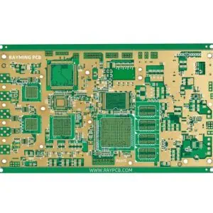
The interconnect system in a PCB consists of multiple layers of conductive material, typically copper, that form the electrical pathways. These pathways include surface traces that route signals across individual layers, through-hole vias that connect different layers vertically, and pads that provide connection points for components. The complexity of modern PCBs, with their multiple layers and high-density interconnections, makes them susceptible to various types of defects that can affect signal integrity, power distribution, and overall system reliability.
Modern PCBs often feature intricate designs with trace widths measured in micrometers, blind and buried vias, and complex layer stackups. This miniaturization and increased complexity have made interconnect defects more challenging to detect and prevent, requiring sophisticated manufacturing processes and quality control measures.
Categories of Interconnect Defects
Interconnect defects in PCBs can be broadly categorized into manufacturing defects, assembly-related defects, and operational defects that develop over time. Manufacturing defects occur during the PCB fabrication process and include issues such as incomplete etching, poor plating quality, or misaligned layers. Assembly-related defects arise during component mounting and soldering processes, while operational defects develop during the PCB’s service life due to environmental factors, thermal cycling, or mechanical stress.
Manufacturing-Related Interconnect Defects
Open circuits represent one of the most common manufacturing defects, occurring when a conductive path is incomplete or broken. This can result from over-etching during the chemical etching process, where excessive removal of copper creates gaps in traces. Under-etching can cause the opposite problem, where insufficient copper removal leaves unwanted connections between adjacent traces, creating short circuits. These defects are particularly problematic in high-density designs where trace spacing is minimal.
Via defects constitute another significant category of manufacturing issues. Incomplete via plating can create high-resistance connections or complete opens between layers. This occurs when the plating process fails to adequately deposit copper within the via barrel, often due to inadequate cleaning, poor plating solution quality, or insufficient plating time. Void formation within vias can also create reliability issues, as these voids can expand under thermal stress and eventually cause connection failure.
Delamination between layers represents a serious structural defect that can affect interconnect integrity. This occurs when the adhesion between the substrate material and copper layers fails, often due to contamination during manufacturing or inadequate surface preparation. Delamination can lead to intermittent connections and eventual complete failure of the affected interconnects.
Assembly-Related Defects
Solder joint defects significantly impact interconnect reliability, even though they technically occur at the interface between the PCB and mounted components. Cold solder joints, characterized by insufficient heat during soldering, create high-resistance connections that can fail under thermal or mechanical stress. Solder bridges between adjacent pads can create unintended short circuits, while insufficient solder can lead to weak mechanical connections and potential opens.
Pad lifting during assembly represents another critical defect where the copper pad separates from the substrate during soldering or rework processes. This typically occurs due to excessive heat application, multiple rework cycles, or poor pad adhesion. Lifted pads can create complete opens in the interconnect system and are often difficult to repair effectively.
Operational and Environmental Defects
Thermal cycling creates significant stress on PCB interconnects due to the different coefficients of thermal expansion between copper conductors and substrate materials. Repeated expansion and contraction can lead to fatigue cracking in traces and vias, particularly at stress concentration points such as corners or areas where traces change width. This thermal fatigue can progress slowly over time, initially causing intermittent failures before eventually creating complete opens.
Corrosion of copper interconnects can occur in environments with high humidity, salt spray, or chemical exposure. Galvanic corrosion can be particularly problematic when dissimilar metals are present, creating electrochemical cells that accelerate copper dissolution. This corrosion can manifest as surface oxidation, pitting, or complete dissolution of thin traces.
Mechanical stress from vibration, shock, or flexing can cause crack propagation in interconnects. This is especially problematic in applications where PCBs are subject to repeated mechanical loading, such as automotive or aerospace applications. Stress concentrations at via locations or trace corners can accelerate crack initiation and propagation.
Detection and Analysis Methods
Visual inspection remains the first line of defense against interconnect defects, utilizing optical microscopy and automated optical inspection (AOI) systems to detect surface-level defects such as opens, shorts, and dimensional variations. However, many interconnect defects are not visible on the surface and require more sophisticated detection methods.
Electrical testing methods include in-circuit testing (ICT) and flying probe testing to verify connectivity and measure resistance values. These methods can detect opens, shorts, and high-resistance connections but may not identify intermittent defects or those that only manifest under specific conditions.
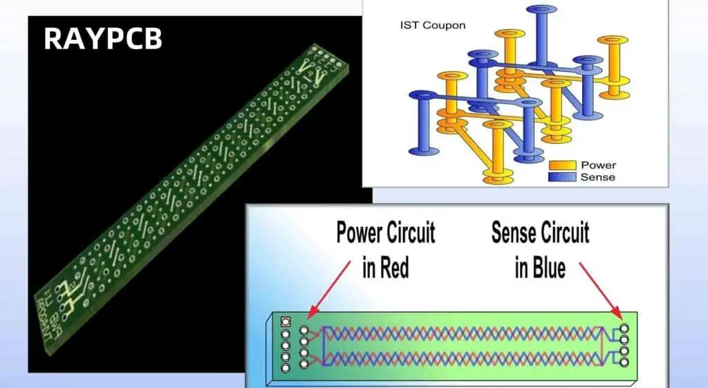
Cross-sectional analysis involves cutting through the PCB to examine the internal structure of vias and layer interfaces. This destructive testing method provides detailed information about plating quality, void formation, and delamination but can only be performed on sample boards.
Time-domain reflectometry (TDR) and frequency-domain analysis can identify impedance discontinuities and signal integrity issues caused by interconnect defects. These methods are particularly useful for high-speed digital applications where signal integrity is critical.
Prevention and Mitigation Strategies
Design for manufacturability (DFM) principles play a crucial role in preventing interconnect defects. This includes appropriate trace spacing, via sizing, and placement to accommodate manufacturing tolerances. Avoiding sharp corners and providing adequate copper area for thermal dissipation can reduce stress concentrations and improve reliability.
Process control during manufacturing is essential for minimizing defects. This includes maintaining proper etching parameters, ensuring adequate surface preparation for plating, and controlling environmental conditions during assembly. Statistical process control (SPC) methods can help identify process variations before they result in defective products.
Material selection significantly impacts interconnect reliability. Using high-quality substrate materials with appropriate glass transition temperatures and coefficients of thermal expansion can reduce thermal stress. Surface finishes such as immersion gold or organic solderability preservatives (OSP) can protect copper surfaces from oxidation and improve solderability.
Impact on System Performance
Interconnect defects can have varying impacts on system performance depending on their location and severity. Complete opens obviously result in non-functional circuits, while high-resistance connections can cause voltage drops, increased power consumption, and potential timing issues in digital circuits. Intermittent connections can create particularly challenging problems, as they may only manifest under specific operating conditions or environmental stresses.
In high-frequency applications, even minor interconnect defects can significantly impact signal integrity. Impedance discontinuities caused by via defects or trace irregularities can create reflections, crosstalk, and electromagnetic interference. These effects can degrade signal quality and reduce system performance even when the basic connectivity remains intact.
Quality Assurance and Testing
Comprehensive quality assurance programs for PCB interconnects must address both manufacturing and operational aspects. This includes incoming material inspection, in-process monitoring during fabrication, and final testing before shipment. Accelerated life testing under elevated temperature, humidity, and mechanical stress conditions can help identify potential reliability issues before they occur in field applications.
Statistical sampling and failure analysis of returned products provide valuable feedback for improving manufacturing processes and design guidelines. This data can be used to refine quality control procedures and identify emerging failure modes that may require process modifications.
Future Challenges and Considerations
As electronic systems continue to evolve toward higher densities, faster speeds, and smaller form factors, interconnect defects will become increasingly challenging to prevent and detect. Advanced packaging technologies such as embedded components and flexible-rigid constructions introduce new potential failure modes that require updated quality control approaches.
The development of new materials and manufacturing processes offers opportunities to improve interconnect reliability, but also introduces new variables that must be carefully controlled. Continued research into defect mechanisms and prevention strategies will be essential for maintaining the reliability standards expected in modern electronic systems.
Understanding and controlling interconnect defects in PCBs requires a systematic approach that addresses design, manufacturing, and operational factors. Through careful attention to these various aspects, manufacturers can produce reliable PCBs that meet the demanding requirements of modern electronic applications while minimizing the risk of interconnect-related failures.