What is PCB Meaning ?

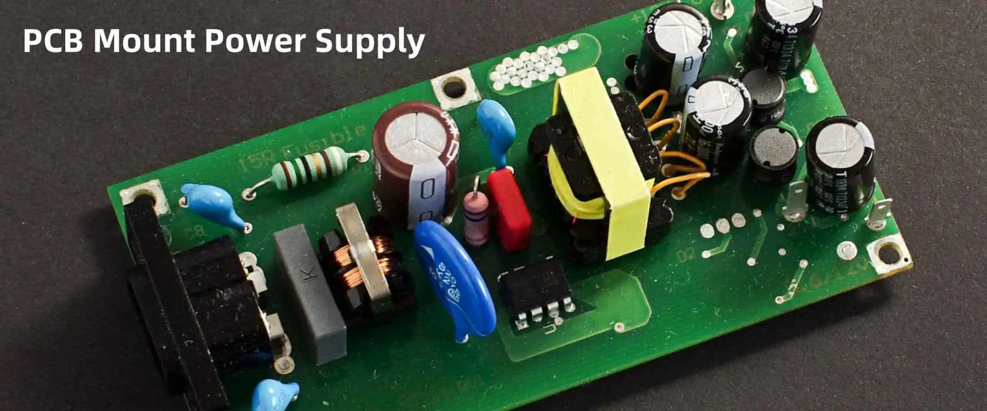
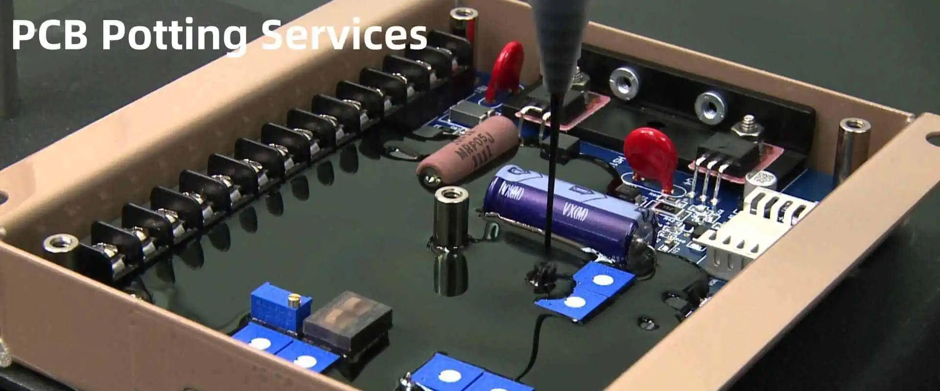
PCB stands for Printed Circuit Board. A PCB is a board used to mechanically support and electrically connect electronic components using conductive pathways or traces etched from copper sheets laminated onto a non-conductive substrate. PCBs are the foundation of almost every electronic device, allowing different components like integrated circuits, resistors, capacitors, and others to be interconnected and work together. Understanding what PCB means helps appreciate the important role PCBs play in electronics and how their design directly impacts the functionality, performance, and reliability of electronic devices.

What Does PCB Stand For?

PCB stands for Printed Circuit Board. Other names for PCBs include printed wiring boards (PWBs) and etched wiring boards. Some key points on what PCB means:

  • PCB refers to the circuit board substrate made from an insulating material like FR-4 fiberglass, on which copper tracks are printed or etched to form the electrical connections between components.
  • The “printed” part of PCB refers to the pattern of copper tracks or circuitry etched on the board which replaces individual wires. This pattern is created through methods like screen printing or photolithography.
  • The use of the word “printed” does not mean PCBs are created by mechanically printing or stamping the wires onto the board. The patterns are painstakingly etched or removed from the copper layer bonded to the substrate.
  • PCB allows the mounting of electronic components like ICs, resistors, capacitors, CPUs etc. which are soldered onto the copper tracks to complete an electronic circuit.
  • Without a PCB, hundreds or thousands of individual wire connections would need to be made between components. The printed board provides organized, optimized, reliable connectivity.

In summary, PCB refers to the copper-laminated non-conductive board that provides the structural base and electrically conductive pathways to connect and power electronic components in a circuit. The board is etched with an intricate “printed” pattern of wiring traces substituted for individual wires. This technique revolutionized circuit assembly, enabling automated, reliable, miniaturized electronics.

A Brief History of PCBs

Customized rigid flex PCB

The earliest predecessor of printed circuit boards dates back to the early 20th century. Here are some key milestones in the history and evolution of PCBs:

  • Early 1900s – Electricians soldered conductors like copper rods or strips directly to panel boards to assemble circuits and terminal equipment. This was labor-intensive, requiring individual wires to interconnect components.
  • 1925 – Techniques emerged to assemble multiple terminal connections by machining grooves into a Bakelite wood-flour composite panel board, into which metal strips were inserted and then soldered.
  • 1936 – The first actual printed wiring board using a precursor of today’s PCB was designed by Paul Eisler. He etched circuits onto Bakelite plates using conductive materials and photomechanical etching.
  • 1940s – The US military began using printed wiring boards for bomb detonators and anti-aircraft proximity fuses during World War II.
  • 1950s – PCBs were produced commercially and became the foundation of circuit assembly for electronic devices. FR-4 glass-reinforced epoxy laminate became the most common PCB substrate.
  • 1970s – Advances in electronics manufacturing allowed greater circuit densities, trace sizes, and automation in PCB fabrication and component assembly.
  • 1980s – Surface-mount technology enabled miniaturized surface-mount components to be soldered directly onto PCBs rather than using wire leads.
  • Today – High-density multi-layer PCBs with elaborate cooling, shielding, and signal integrity enhancements are the backbone of cutting-edge electronics. New materials like ceramics and flexible substrates also expand PCB capabilities.

PCBs have evolved enormously, but still serve the same vital purpose – providing a structurally sound foundation to electromechanically support and connect electronic components using etched conductive copper pathways.

What is a PCB Made of?

A PCB consists of an insulating substrate reinforced with epoxy resin, onto which a layer of copper is laminated on one or both sides to create the conductive pathways between components. Here are the main constituent materials of a typical rigid PCB:

  • Substrate – Usually a glass reinforced epoxy laminate sheet called FR-4. Other options include composites like FR-1 paper-phenolic and flexible substrates like polyimide.
  • Conductors – Typically a thin sheet of copper foil (1 oz/ft2 or 35 ฮผm) laminated to one or both sides of the substrate. Other conductor options include aluminum and silver.
  • Dielectric Layer – The epoxy resin prepreg layer that bonds the conductive foils to the core substrate and insulates copper layers in a multilayer PCB. Common prepregs include FR-4 and polyimide.
  • Finish – Coatings applied on top of conductors to protect and facilitate soldering. Common finishes include organic solderability preservatives (OSP), immersion tin, immersion silver, gold plating.
  • Silkscreen – Epoxy ink printed on the PCB to label components and polarities, usually white or yellow.
  • Solder Mask – Epoxy layer that coats the PCB covering copper traces, exposing only the solder pads. Usually green color.
  • Drilled Holes – Holes drilled through the PCB substrate to allow leads or wires to pass through and connect layers. Plated with copper.

While FR-4 fiberglass is the most common, a wide range of substrate materials like Rogers, polyimide, Teflon, and others can be used. Different materials provide various benefits in performance, temperature tolerance, flexibility, volume manufacture, and cost.

How is a PCB Fabricated?

PCBs are fabricated using the following general sequence of steps:

  1. Design – The PCB layout is designed in software like Eagle, Altium or KiCad. The schematic and board outlines are drawn.
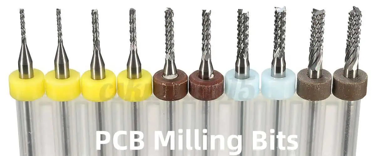
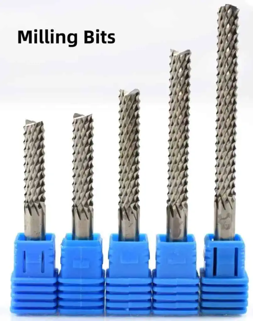
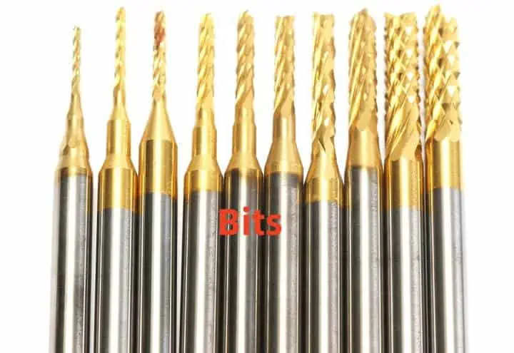
  2. Prototyping – For simple circuits or testing, DIY methods like milling or toner transfer can create single PCBs.
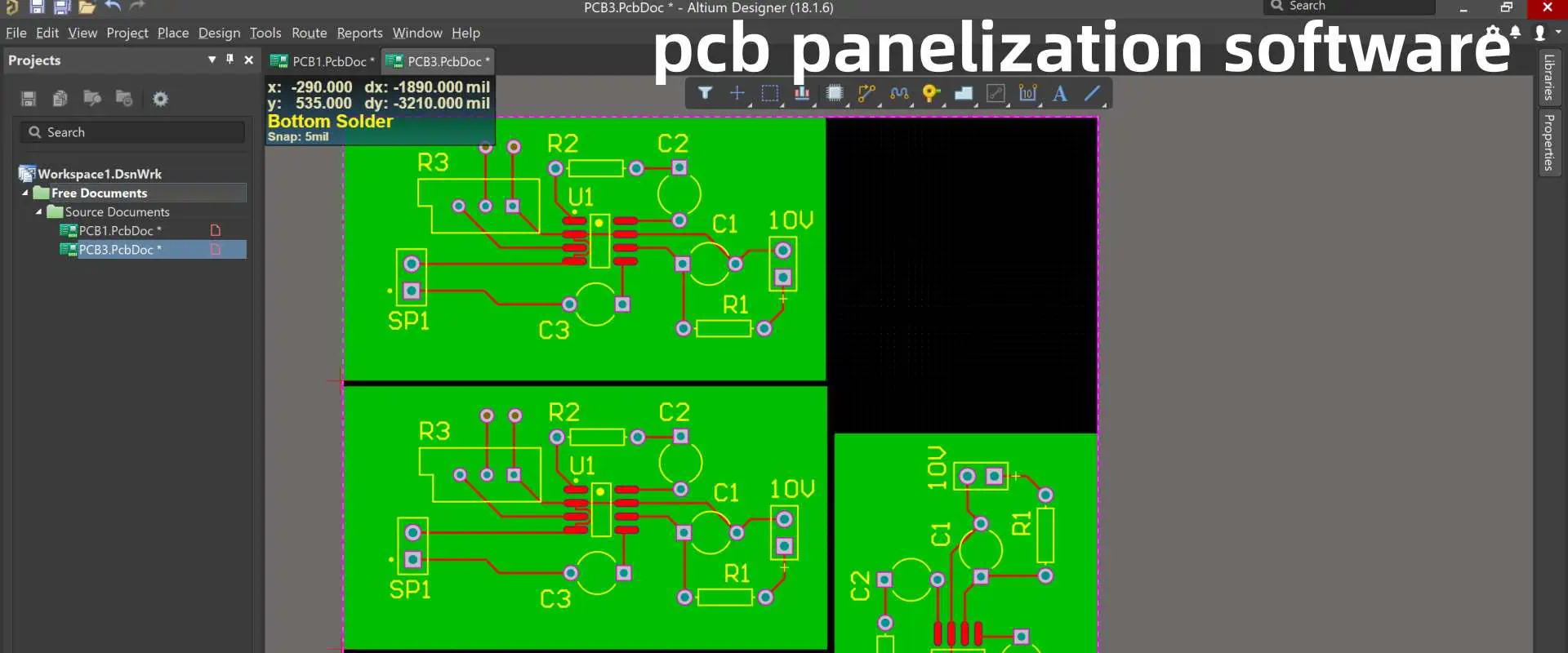
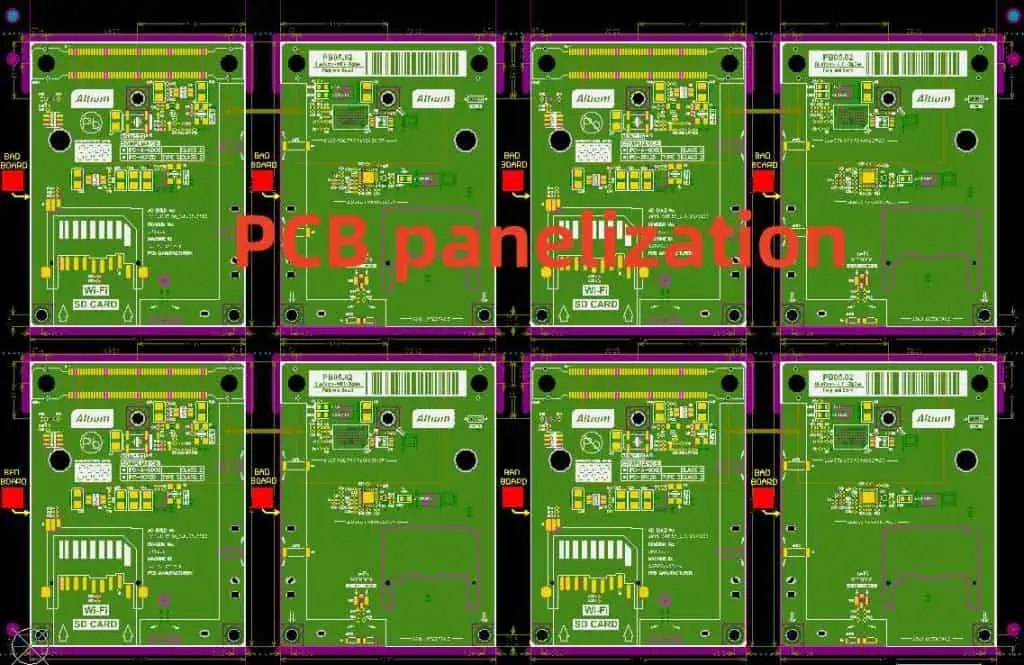
  3. Panelization – For volume production, the PCB design is replicated in a panel for mass lamination.
  4. Lamination – Sheets of copper-clad substrate are stacked with prepreg dielectric layers and laminated under heat and pressure.
  5. Drilling – Holes are precision-drilled for component leads using small drill bits, often controlled by a CNC drill machine.
  6. Plating – Walls of drilled holes are plated with copper to electrically connect layers of the PCB.
  7. Etching – Unwanted copper is selectively removed by chemical etching to leave only the desired conductive copper traces on the substrate.
  8. Solder mask – UV-curable epoxy layer is applied by spraying, screen printing or photo-imageable process.
  9. Silkscreen – Component outlines and identifiers are screen printed on the solder mask ink.
  10. Routing – Individual PCBs are routed or cut from the larger panelized boards.
  11. Testing – Quality checks are performed, including electrical testing, visual inspection, and x-ray.
  12. Assembly – Electronic components are soldered onto the fabricated PCB.

The specific fabrication steps and sequence may vary across different PCB manufacturers and for specialized PCB technologies. But this gives a general idea of the PCB fabrication process.

PCB Classifications

PCB IPC standards

PCBs can be classified based on the number of conductive copper layers or “sides” as follows:

Single-sided

  • One copper layer, usually on top side of substrate. Components mounted on same side.

Double-sided

  • Two copper layers, one on each side of substrate. Allows increased component density.

Multilayer

  • Has three or more copper layers laminated with insulating dielectric, interconnected by plated through-holes. Allows greater complexity.
  • Most common are 4-layer and 6-layer, but can go up to 32 layers or more.
  • Outer two conductive layers are for component mounting. Inner layers are for power distribution and signal traces.

In addition to layer count, PCBs can also be classified by conductive pattern fabrication technique:

  • Printed Circuit Boards (PCB) – Circuits etched from copper laminated on substrate.
  • Printed Wiring Boards (PWB) – Wiring traces are printed by plating into a blank pattern.

As well as types of substrate materials:

  • FR-4 Boards – Most common. Made from glass reinforced epoxy resin.
  • Flexible Circuits – Made from polyimide, flex PCBs can bend and twist. Used for wearables or space-constrained devices.
  • Metal Core PCBs (MCPCB) – Aluminum or copper substrate removes heat from power components.
  • High-frequency Boards – Use low-loss dielectric substrates for RF/microwave circuits.
  • Ceramic Boards – Used for robust high-temperature automotive or aerospace electronics.

And there are many other classifications as PCB technology continues advancing. But layer count, fabrication process, and base substrate are the main categories for differentiating PCB types.

PCB Design and Layout

Creating the physical layout and wiring plan for a PCB is a skilled task mixing engineering design with software CAD tools. Here is a simplified overview of the PCB design and layout process:

Schematic Capture

  • The electronic circuit is mapped out in schematic diagram form using CAD software like Eagle, OrCAD, Altium, KiCAD etc.
  • Symbols represent each component and lines between them represent conductive connections.
  • The schematic captures the logical electronic functionality without indicating physical position.

Floorplanning

  • The physical board dimensions and component placement is determined based on parameters like desired device size, shape, component sizes, and required clearances.
  • Critical traces may be mapped out beforehand between points where key components must connect.

Layout

  • Components are arranged and routed on the board canvas. CAD tools allow the layout to be flipped and rotated while visualizing trace clearance.
  • Traces are neatly laid out connecting nodes between components following established routing conventions like 45-degree angles and minimizing crossovers.
  • Simulation checks can identify issues like electrical noise, signal reflections, power delivery problems, or electromagnetic interference that may impact performance.
  • The designer ensures specifications are met and design rules adhered to. Numerous adjustments are made iteratively to optimize the layout.

Final Output

  • Manufacturing files like Gerber files, drill files, and IPC-356 testpoint report are generated. Many output file types are needed by PCB fabricators.
  • Final design validation is done before releasing to fabrication.

While simplified, this captures the progression from functional schematic to physical PCB layout while balancing electrical performance, manufacturability, and cost constraints.

Applications and Advantages of Using a PCB

military-grade-pcb-manufacturing

Here are some of the key applications and benefits that make PCBs an indispensable technology across nearly all modern electronics:

  • Circuit Miniaturization – PCBs allow extremely small and complex circuits to be reliably mass-produced – a feat impossible with individually assembled wires.
  • Organized Layout – PCBs allow optimized component placement and routing to minimize electrical noise and enhance performance.
  • Cost Efficiency – Automated PCB production is extremely cost-effective compared to manual wiring and soldering.
  • Reliability – PCB assembly eliminates wiring errors and loose connections prone with point-to-point wiring.
  • Serviceability – Individual failed components can be desoldered and replaced quickly.
  • Multi-layer Circuits – Multilayer PCBs allow complex, high-density interconnections between components.
  • Component Mounting – PCBs provide firm mechanical support and electrical terminals for mounting components like ICs, resistors, connectors etc.
  • Ease of Assembly – Automated PCB assembly, soldering and test processes can be implemented with proper design.
  • Heat Sinking – Some PCB substrates like MCPCBs and ceramics excel at conducting heat from high-power components.
  • System Integration – PCBs allow integration of circuits, microprocessors, memory, sensors and other technologies into a unified system.

From the integrated circuits powering supercomputers to LED throwie art projects, PCBs enable nearly all modern electronic devices. Correct PCB design ensures the device performs properly, reliably, and safely.

Common PCB Terminology

There are many industry terms associated with PCBs that are good to know:

  • Traces – The copper lines that form the electrical connections between points on a PCB. Also called tracks.
  • Pads – Metallic areas on the PCB where component leads or wires are soldered to traces.
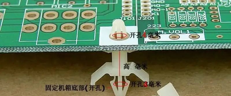
  • Plated-through Hole (PTH) – Holes drilled in a multilayer PCB with metal plating to interconnect layers. Also called vias.
  • Annular Ring – Ring of clear space around a drilled hole, important to ensure reliable plating.
  • Jumper – Short trace “jumping” over a trace or component to connect two points without intersecting.
  • Plane – Large copper area used for power distribution or heat dissipation.
  • Breakout Board – Small board that connects headers to various individual pinouts or ports as a transition to cable connectors.
  • Keepout – Area of bare board that must be kept clear of copper and components, usually for clearance. Denoted on silkscreen.
  • Tenting Vias – Covering the top and bottom of a via with solder mask to prevent solder from plugging via barrel during reflow.
  • Castellated Holes – Half-drilled plated holes along the board edge allows surface mount soldering to external connectors or daughterboards.

And many additional terms for via types, hole shapes, trace widths, junctions, lands, thermal relief, testpoints and other PCB features. The expansive terminology reflects the extensive engineering considerations made in PCB design.

Key Factors in PCB Design

Modular PCB Design
Modular PCB Design

Designing a functional, reliable printed circuit board requires careful consideration of electrical, thermal, and mechanical factors:

  • Circuit Function – Does the PCB schematic and layout accurately produce the intended behaviors of the target electronic circuit or system? Verification requires testing and simulation.
  • Trace Current – Track widths must be sized appropriately for the expected current flows to avoid overheating and maintain signal integrity.
  • Impedance Control – Matching trace impedances to terminal impedances prevents signal reflections and unintended inductances.
  • Noise Reduction – Careful routing and ground planes suppress electrical noise and crosstalk, especially at high frequencies.
  • Power Distribution – Power and return paths must be adequate for all component power needs. Planes help here.
  • Thermal Loads – Copper planes or thermal vias help conduct heat out of high power components.
  • Mechanical Strength – Materials and stackup must provide sufficient strength, especially where connectors attach.
  • Manufacturability – Design must adhere to fabricator capabilities and domain-specific guidelines like IPC standards.
  • Testability – Incorporating testpoints and vias for probing aids defect analysis and troubleshooting.

The PCB designer has responsibility for considering all these aspects and more to create a functional board that can be economically manufactured and works reliabily.

PCB Design Software

There are many PCB design software options at a range of prices, features, and complexity:

SoftwareDescription
EaglePopular entry-level tool owned by Autodesk. Available as free version with limited board size.
KiCadFull open-source suite with schematic capture, routing, and 3D viewing. Steep learning curve but very powerful.
Altium DesignerIndustry-leading tool with unified design environment. High cost but advanced features.
OrCADFull PCB design solution from Cadence with tight integrations between schematic, layout, and analysis tools.
DipTraceAffordable tool especially good for multi-layer boards. Downsides are performance issues at larger board sizes.
EasyEDAPopular online entry-level tool with free version. Limited feature set compared to downloads.
FritzingOpen-source tool focused on artists, students, and hobbyists. Breadboard sketching and hardware interaction are strengths.
MultisimCircuit simulation tool useful during schematic design to verify electronic behaviors before layout.

And there are many other options. Key considerations when selecting PCB design software include cost, features, usability, output file generation, simulation/analysis capabilities, manufacturer integrations, and whether online or desktop install.

Recent Advances in PCB Technology

Some leading-edge developments in PCB tech:

  • High-Density Interconnects (HDI) – Very dense trace routing and microvias, reducing layer count. Used in advanced consumer electronics.
  • Embedded Components – Capacitors, resistors and other discrete passives buried inside the PCB layers. Saves space and cost.
  • Flex and Rigid-Flex – Allows integrating rigid and flexible polyimide boards. Useful for wearables and compact folding.
  • Stretchable Circuits – Novel materials and manufacturing methods now allow stretchable, flexible PCBs.
  • Panel Plating – Plating internal layers and drilling vias while the PCBs are still in panel form for efficiency.
  • Additive Processes – Additive deposition methods like inkjet and aerosol printing can directly “print” conductive traces, avoiding etching.
  • RF/Microwave – Improved modeling and materials enable higher frequency boards above 3GHz. Key for communications.
  • Automated Assembly – Emerging “lights out” production lines with AI-driven machines to enable highly automated PCB production.

And many other recent improvements allow PCBs to drive performance and integration in cutting-edge tech like IoT, EVs, 5G, and mobile devices.

Top 15 PCB Requirements in medical devices (Recommend)

medical grade pcb

Printed circuit boards (PCBs) are critical components enabling the functionality of medical devices like patient monitors, imaging systems, diagnostics equipment, and therapeutic devices.

The PCBs in medical equipment have stringent design, performance, quality, and regulatory requirements to ensure patient safety and reliability. This article outlines the key considerations for medical PCBs across electrical, mechanical, manufacturing, and regulatory factors.

Electrical Design Requirements

Medical devices impose demanding electrical requirements on PCB design.

1. Low Leakage, Low Noise

Medical signals require amplification and processing of very low voltages down to microvolt levels. This mandates:

  • Minimizing leakage currents in bias circuits
  • Preventing digital switching noise in analog areas
  • Careful stackup and layout for signal integrity
  • Proper grounding, filtering, and shielding

Even small amounts of noise or interference can corrupt tiny physiological signals or sensor outputs.

2. Isolation and Safety

Patient contact circuits need high levels of isolation from line voltages to prevent any electrical hazard shock risks. Key measures include:

  • Reinforced isolation barriers and creepage distances
  • Opto-isolators for signals crossing isolation zones
  • Split power supplies to maintain isolation
  • Proper dielectric spacing in PCB stackup
  • UL, IEC safety certifications for components and materials

3. EMI and ESD Control

The EMI emissions and immunity levels are tightly regulated for medical equipment, requiring:

  • Low-noise components like crystal oscillators
  • Board-level shielding of circuits
  • Careful component placement and routing
  • Liberally used filtering and protection

Robust ESD protection also prevents damage to sensitive inputs.

4. Component Derating

Components must be operated well below rated voltages and temperatures to improve long-term reliability. Key practices:

  • Derating voltages by 20% or more
  • Limiting power dissipation to 50% or less of max ratings
  • Using larger package sizes than electrical need
  • Providing design margin in clock speeds and duty cycles
  • Sufficient cooling for heat-generating components

Mechanical Design Requirements

Medical Devices pcb
Medical Devices pcb

Medical PCBs must withstand constant use in demanding mechanical environments.

5. Vibration and Shock Resistance

Equipment vibration from fans, pumps, and transportation along with occasional shocks require:

  • Interposers, frame mounts, and fasteners to strengthen solder joints
  • Conformal coating to prevent surface mount cracks
  • Avoiding heavy connectors and components in shock-prone locations
  • Careful use of stiffeners, brackets, or backplanes
  • Analysis of resonance frequencies and modes

6. Durability and MTBF

Medical products demand high mean time between failures (MTBF) exceeding 20000 hours. Durability requires:

  • Component derating as mentioned
  • FEA analysis to avoid mechanical weaknesses
  • HAST, temp cycling, drop testing to verify robustness
  • Avoiding BGAs and other fragile packages
  • Conformal coating, potting, or encapsulation
  • Statistical analysis of failure rates

7. Thermal Management

Sustained reliable operation requires preventing overheating through:

  • Generous ground planes and thermal vias
  • High thermal conductivity substrates
  • Heat sinks, fans, and airflow pathways
  • Thermal modeling to identify hot spots
  • Temperature monitoring circuitry
  • Screening components for desired temperature grade

Manufacturing Requirements

Medical PCBs demand tightly controlled manufacturing and inspection.

8. Biocompatibility

All materials must be biocompatible for any patient contact, including:

  • Substrate laminates
  • Solder masks, finishes, and adhesives
  • Component lead materials

Common biocompatible options are FR4, immersion silver coating, and nickle-free solder.

9. Cleanliness

Stringent cleanliness prevents contamination that can impact performance. Requirements:

  • Assembly in ISO Class 7 or better cleanrooms
  • Solvent cleaning of boards and components
  • Laminar airflow assembly stations
  • Package singulation outside cleanrooms
  • Prevention of human contact with assembly materials

10. Traceability

Full traceability for the life of the product enables tracking all materials, components, manufacturing details, inspection results and repairs, supported by:

  • Serialization marking on boards
  • Raw material and component lot/batch tracking
  • Comprehensive data collection and ERP systems
  • Labeling and scanning procedures
  • Detailed equipment maintenance logs

Traceability facilitates root cause analysis and containment in the field.

11. Testing and Inspection

Extensive testing to specifications and standards ensures reliability:

  • Repeated electrical testing under temperature cycling
  • X-ray inspection of internal features like vias
  • Automated optical inspection (AOI) for assembly flaws
  • Solder joint inspection – 2D and 3D scanning
  • In-circuit testing (ICT) for shorts, opens, values
  • Functional testing under use-case scenarios

12. Change Management and Control

Engineering change control processes manage revisions to:

  • Confirm continued compliance with requirements
  • Full regression testing for affected parameters
  • Prototyping to validate changes
  • Gaining regulatory re-approval as needed

Regulatory Requirements

medical-pcb

Medical devices sold worldwide must satisfy different country regulations.

13. UL and IEC 60601 Certification

These overlapping standards establish safety criteria like:

  • Leakage current limits
  • Dielectric voltage withstand
  • Fault tolerance
  • Component spacing/creepage
  • Protective earth/grounding
  • Enclosure ingress protection ratings
  • Marking and labeling

Certification demonstrates compliance to reduce risk.

14. FDA and CE Approval

Regulatory approval is required to market and sell devices. Key steps are:

FDA

  • Device classification
  • Premarket notification 510(k)
  • Submission of testing and design data

CE Marking

  • Conformity assessment
  • Technical file and risk management documentation
  • Review by Notified Body
  • Declaration of Conformity

Re-approval is needed for significant changes.

15. ISO 13485 Quality Management

Implementing ISO 13485 ensures continuous quality:

  • Infrastructure – cleanrooms, ESD control, utilities
  • Process controls – SOPs, ECOs, supplier management
  • Training records
  • Traceability and document control
  • Risk management procedures
  • Quality auditing

Robust certified quality systems satisfy regulators and improve outcomes.

In summary, designing and manufacturing PCBs for medical applications demands rigorous attention across electrical, mechanical, thermal, cleanliness, reliability, traceability, testing, and regulatory factors to achieve safe and effective performance.

Best Practices for Medical PCB Development

medical pcb assembly

Follow these best practices when developing PCBs for medical devices:

  • Maintain superb EMI/EMC and signal integrity through careful stackup design, routing, filtering, and shielding.
  • Incorporate extensive safety measures for electrical isolation and biocompatibility of materials.
  • Perform thorough thermal analysis and heat sinking to dissipate heat from components.
  • Utilize advanced modeling, simulation, and analysis techniques to validate the design.
  • Subject prototypes to aggressive testing under voltage, temperature, vibration, and longevity scenarios.
  • Employ stringent manufacturing and inspection controls for cleanliness, process variability, soldering, etc.
  • Maintain excellent traceability and change control throughout the product lifecycle.
  • Rigorously satisfy all pertinent regulatory, safety, and compliance standards.
  • Utilize certified quality systems and proven program management methodology.
  • Partner with experienced, proven suppliers and engineering teams knowledgeable in medical requirements.

Conclusion

Medical PCBs call for a diligent design approach covering electrical, mechanical, manufacturing, and regulatory factors critical for product efficacy and safety in sensitive life-critical applications.

Careful management of noise, isolation, materials, reliability, inspection, traceability, and compliance ultimately provides peace of mind that patients are protected from harm.

With sound engineering discipline, regulation, and quality systems implementation, PCBs can be successfully developed to enable breakthrough medical advancements.

Frequently Asked Questions

Q: What are some good substrate choices for medical PCBs?

Some commonly used substrates include:

  • FR4 – Cost-effective, can achieve UL94 V-0 flammability rating
  • PTFE/ceramic filled – Increased thermal performance
  • Hydrocarbon ceramic – Superior high frequency properties
  • Polyimide – Excellent thermal shock resistance
  • Rogers laminates – Tight dielectric constant and loss control

Isola, Arlon, and Park/Nelco are leading medical material suppliers.

Q: How can medical equipment achieve immunity to ESD?

Typical ESD protection measures:

  • TVS diodes across I/O signals
  • High pass filtering to attenuate ESD transients
  • Series resistors to limit energy entering board
  • Shielding of exposed connectors and cables
  • ESD coatings like zinc whiskers
  • Antistatic materials and grounding

Q: What are important considerations for PCBs going in portable medical devices?

For portable designs:

  • Withstand shock from drops and impacts
  • Minimize electromagnetic emissions for compliance
  • Handle widely varying thermal conditions
  • Optimize power consumption for battery life
  • Prevent external contaminants like dust and moisture
  • Accommodate battery interfaces and charging circuitry

Q: What are some key standards applicable to medical PCBs?

Relevant standards bodies:

  • UL – UL60601-1, flammability ratings
  • IEC – IEC60601-1, general safety
  • ISO – ISO13485, quality management
  • FCC – EMI emissions limits
  • AAMI – Association for the Advancement of Medical Instrumentation

Q: How can change management help with medical PCB updates?

Effective change management:

  • Reduces inadvertent introduction of faults
  • Maintains traceability between revisions
  • Forces proper failure analysis before changes
  • Ensures extensive re-verification after changes
  • Provides documentation for regulators on changes
  • Prevents unwanted cost and timeline impacts

How to Choose PCB Milling Bits for Routing ?

PCB milling uses a rotating endmill tool to cut away unwanted copper from a board to fabricate traces and isolation. Selecting the right milling bit is crucial for achieving good routing quality and productivity.

Key bit parameters like diameter, tip shape, coating, and material significantly impact performance. This article provides guidance on choosing optimal PCB milling bits based on board requirements and machine capabilities.

PCB Milling Process Overview

PCB milling employs a multi-axis mechanical platform to position a spinning endmill over a copper-clad board. The milling bit cuts away copper to fabricate isolation gaps and circuit conductors based on programmed toolpaths.

Key stages in the milling process:

  • Clamping material blank onto machine bed
  • Aligning board origin reference
  • Loading milling bit into spindle
  • Setting spindle speed and feed rates
  • Importing isolation and routing toolpaths
  • Executing toolpaths to cut board features
  • Unloading finished board

Milling provides a flexible digital fabrication approach for rapid PCB prototyping without chemicals. The right bit helps balance quality and speed.

Key Factors in PCB Milling Bit Selection

Consider the following parameters when selecting a bit for PCB milling:

Bit Diameter:

  • Smaller diameters allow finer details and cuts
  • Larger diameters remove material faster with less tool stress

Tip Shape:

  • Ball end vs flat end have different cutting characteristics
  • End cutting vs center cutting impact edge finishes

Flute Geometry:

  • Number of flutes affects removal rate and tool strength
  • Flute length impacts composite cutting and chip clearance

Coating:

  • Uncoated, TiN, TiCN etc. influence tool wear, friction, heat
  • Insulating coatings prevent copper buildup and shorting

Material:

  • Carbide, Cobalt, tool steel have different hardness and wear resistance
  • Material must withstand high RPM without fracturing

Matching bit properties to the board material, layer stackup, line widths, tolerances and target milling time ensures optimized PCB routing.

Bit Diameter

Bit diameter is the most basic factor influencing the milling process. Diameter ranges from around 100 microns up to 6.35 mm (1/4″) or larger are commonly used for PCB milling.

Considerations for bit diameter:

  • Finer lines/spaces โ€“ Smaller bits allow thinner traces and finer pitch. 100um sufficient for 0.5mm lines.
  • Component areas โ€“ Small bits can cutout small chip packages and connectors.
  • Drilling holes โ€“ Bit must be smaller than desired hole size.
  • Large board areas โ€“ Larger bits mill board outlines faster. 3-6mm range useful.
  • Layer material โ€“ Bits sized for substrate rather than just copper thickness.
  • Machine limits โ€“ Spindle power determines max bit size possible.
  • Tool deflection โ€“ Larger bits resist deflection with tool length.
  • Tool life โ€“ Smaller bits wear faster with smaller cross-section.

Selecting bit diameter requires balancing these considerations for the particular board layout. 2mm, 1mm and 0.5mm are commonly used sizes.

Bit Tip Shape

Milling bits come in ball nose and flat/square end shapes. The tip shape impacts cutting performance and edge finish:

Ball Nose Bits

  • Radius tip with round cutting edges
  • Mainly cuts with tip surface not sides
  • Leaves curved path with rounded corners
  • Less prone to chipping edges
  • Cuts smoother ramped sidewalls
  • Ideal for 3D surfacing and contour milling

Flat/Square End Bits

  • Cutting occurs both at tip and along sides
  • Leaves flat bottoms with sharp corners
  • Machines vertical walls with minimal taper
  • Requires more rigid machine since side-cutting is harder
  • Produces fine finish on flat surface areas
  • Must avoid plunging into material

Ball nose tools are commonly used for isolation routing while flat endmills are suitable for trace fabrication. The toolpaths must suit the bit tip style.

Bit Coatings

Applying specialized coatings onto milling bits enhances certain properties:

Uncoated Bits

  • Least expensive option
  • No added performance benefits
  • Prone to galling and adhesion of material

Titanium Nitride (TiN) Coated

  • Thin gold-colored ceramic coating
  • Reduces friction and heat generation
  • Improves tool life 2X over uncoated carbide
  • Resists buildup of material on cutting edges

Titanium Carbonitride (TiCN) Coated

  • Gray ceramic coating
  • Excels in high speed machining situations
  • Tool life 3-5X over uncoated carbide
  • Withstands higher cutting temperatures

Insulating Coatings

  • Prevent conductive tool material shorting signals
  • Required for milling multilayer boards
  • Diamond or silicon nitride coatings commonly used

Coatings improve milling performance for longer tool life, higher feeds/speeds, and multilevel boards. The benefits merit the extra cost over uncoated tools.

Flute Geometry

The flutes of an endmill are the spiral cutting grooves running along the tool body to the tip. Flute characteristics impact milling behavior:

Number of Flutes

  • 2 to 6 flutes common for PCB tools
  • More flutes allow higher feed rates but require more rigid setup
  • Fewer flutes provide easier swarf/debris clearance

Flute Length

  • Longer flutes allow cutting with tool sidewall
  • Helps dissipate heat over larger contact area
  • Requires rigid machine and clamping to prevent deflection

Flute Pitch/Helix Angle

  • Affects direction of chip flow and evacuation
  • Variable helix improves shearing and chip clearance

Flute Profile

  • Square end flutes suitable for slotting
  • Radiused flutes for high feed contouring

Selecting suitable flute characteristics improves milling productivity and workpiece finish.

Bit Composition and Hardness

Carbide endmills are predominantly used for PCB milling due to the required hardness and wear resistance when machining copper.

Some important material properties:

  • Hardness – Harder grade carbides better sustain cutting forces without excessive wear.
  • Fracture Toughness – Carbide must resist chipping at high RPM speeds.
  • Heat Tolerance – High heat is generated, requiring thermal shock resistance.
  • Chemical Compatibility – Some carbide grades may react with copper.
  • Insulating Properties – Tool material should not short circuit conductors when wet.

Cobalt-enriched micrograin tungsten carbide grades offer a good balance of hardness, toughness and conductivity. The carbide grade should match the application and parameters.

Tool Length

Longer endmills inherently deflect more than short mills due to the extended flutes. Deflection reduces routing dimensional accuracy.

Guidelines for tool length:

  • Use shortest tool that fully cuts board thickness
  • For thin boards, bits longer than material can be helpful
  • Limit length to around 2-4X bit diameter
  • Ensure stiff machine, fixtures, collets and toolholding
  • Reduce ramping into material to limit tool loads
  • Run slower feeds/speeds for long thin tools
  • Perform test cuts to verify rigidity and precision

Keeping tool length to the minimum required reduces deflection for better milling precision.

Summary of Bit Selection Considerations

ParameterKey Factors
DiameterFeature size, tool loads, machine power
Tip ShapeContouring vs vertical walls, plunge requirements
CoatingTool life, friction/heat reduction, insulation
Flute GeometryMaterial removal, chip clearance, tool strength
CompositionHardness, toughness, heat resistance, conductivity
LengthDeflection/rigidity, tool extension, precision

Balance these interdependent factors to select tooling providing the optimum combination of capability, productivity and accuracy for the target board.

Milling Bit Suppliers

Many companies offer endmills suitable for PCB routing and isolation. Some notable carbide PCB tooling suppliers include:

  • Harvey Tool – Wide range of tool diameters/geometries for PCB
  • Lakeshore Carbide – Specializes in miniature endmills
  • Datron – Tools designed for their own PCB milling machines
  • Kyocera – Recognized for micro-tooling expertise
  • Mitsubishi – Leading producer of carbide endmills
  • OSG – Diverse micro-machining tool line
  • Performance Micro Tool – Ultra small diameter tools

The range of bit parameters offered by these manufacturers facilitates dialing in a tooling solution tailored to the application requirements.

PCB Routing Toolpath Considerations

The toolpath strategy used for milling must suit the bit characteristics selected. Key factors:

Direction:

  • Along trace axes vs diagonal gives different finish and edge quality.

Stepover:

  • Lateral spacing between toolpath passes impacts material removal rate and surface finish.

Contouring:

  • Manage transitions between straight and curved toolpaths to limit gouging.

Entry/Exit Moves:

  • Control bit ramping into material for clean entry starts and exits.

Climb vs Conventional Milling:

  • Climb milling loads bit less. Conventional clears debris better.

Tolerance:

  • Tighter path tolerance for smaller tools and features.

Feeds/Speeds:

  • Optimize for tool size, materials, coatings etc. Start conservative.

The toolpath strategy complements bit characteristics for optimal routing effectiveness.

Summary

Key takeaways on selecting PCB milling bits:

  • Match bit diameter, tip shape, coating and material properties to board requirements.
  • Smaller bits enable high resolution details but limit material removal rate.
  • Ball nose bits excel at 3D contouring while flat endmills machine vertical walls cleanly.
  • Coatings like TiCN boost tool life and performance significantly over uncoated tools.
  • Optimal flute geometry improves swarf evacuation, tool strength and cutting capability.
  • Rigid, precision fixturing is critical for thinner, longer tools prone to deflection.
  • Toolpath strategy must suit bit geometry and parameters.
  • Obtain endmills from reputable carbide tooling specialists.

Choosing the best PCB milling bit for the application results in reduced tool wear, improved surface finish, faster milling time, and greater dimensional accuracy.

Frequently Asked Questions

Q: What drill bits can be used for making holes in circuit boards?

For hole drilling, small diameter twist drills made from cobalt steel work well for clean results. Carbide drill bits are also an option but more costly. Uncoated 1/64″ to 1/32″ drills at high RPMs drill holes neatly in typical 0.062″ PCB thickness.

Q: What are the downsides of using a bit that is too small?

Using an overly small bit has some disadvantages:

  • Requires slower feed rates to avoid tool failure
  • Prone to rapid tool wear and breakage
  • Deflection effects more significant
  • Much longer milling time for bulk material removal
  • Higher chatter and poorer surface finish

Avoid bits well under 50% of minimum feature sizes.

Q: What are some signs of a worn out milling bit?

Indications of tool wear:

  • Visible rounding, chipping, fraying of cutting edges
  • Increased cutting forces and torque
  • Higher noise levels and vibration
  • Decline in dimensional accuracy
  • Deteriorating surface finish
  • Uncut copper, burring, rough edges
  • Smoke from higher friction

Replace or resharpen tool promptly when wear is detected.

Q: How should milling bits be stored between uses?

Recommended storage practices:

  • Use bit holders or organized rack systems
  • Avoid loose storage where bits can contact each other
  • Prevent exposure to moisture and chemicals
  • Protect cutting edges from damage
  • Ensure stable temperature conditions
  • Clean bits after use and apply anti-corrosion oil
  • Check for any signs of corrosion periodically

Proper care preserves tool life.

Q: How can deflection from long thin bits be reduced during milling?

Strategies to minimize deflection:

  • Shorten flute length where possible
  • Increase tool diameter relative to stickout
  • Reduce depth of ramping into material
  • Use most rigid holding method – hydraulic, heat shrink
  • Lower feedrates and spindle RPM
  • Ensure setup, fixture, stock are completely secure
  • Verify tool runout is minimal
  • Upgrade to stiffer machine if needed

Eliminating all sources of play and flex dramatically improves results.

How to Mount Power Supply to PCB

Power supplies are vital components that provide the operating voltages and currents required by electronic circuits and systems. Selecting the appropriate power supply and mounting technique is an important part of the overall PCB design process.

Power supplies come in different forms like AC-DC wall adapters, DC-DC converter modules, and open frame power supplies. Most board-level DC-DC converters and open frame supplies are designed for direct mounting onto the PCB itself.

This article provides guidance on PCB design considerations, mounting approaches, thermal management, and best practices for integrating different types of power supplies onto printed circuit boards.

Power Supply Mounting Options

Power supplies meant for PCB mounting typically offer some combination of through-hole pins, surface mount pads, and mechanical mounting features. The best mounting method depends on parameters like:

Some common power supply mounting schemes are:

Through-Hole Pin Mounting

The power supply connector/pinout matches a thru-hole pattern on the PCB for insertion and soldering. Typically requires wave soldering process. Provides strong mechanical coupling. Good for high vibration environments.

Surface Mount Pad Mounting

Surface mount footprints allow reflow soldering of the power supply. Requires less PCB area but heat transfer may be worse. Not ideal for heavy power supplies.

Screw/Standoff Mounting

The power supply fastens onto standoffs or spacers on the PCB using corner screws. Provides very robust mechanical attachment. Requires some manual assembly.

Panel Mounting

Power supply is mounted into a cutout on a metal bracket or chassis panel. Wiring then connects panel interface to the PCB. Useful when board space is unavailable.

DIN Rail Mounting

DIN rail clips allow mounting to standard DIN rails in industrial enclosures. Requires separate DIN rail allocation.

Adhesive Mounting

Suitable for lightweight supplies. Can accommodate uneven surfaces. Generally less robust and permanent.

Key Selection Considerations

Some important aspects when selecting a power supply for PCB mounting:

1. Board Area: Dimensional footprint – height, length, width. Avoid overlaps with adjacent components.

2. Mounting Holes: Spacing, diameter, pad type. Match PCB capability and assembly process.

3. Pinout: Layout of power, signal, control pins. Compatible with PCB layers and routing?

4. Connector Options: Terminal blocks, pin headers, wire leads. Easy integration?

5. Heat Dissipation: Will PCB area provide sufficient cooling surface?

6. Structural Strength: Weight, center of gravity. PCB can support without flexing?

7. Reliability: Vibration, shock resistance rating. Thermal stress on solder joints?

8. EMI/EMC: Noise emissions, susceptibility issues? Filtering or shielding needed?

9. Safety Standards: Applicable certifications – UL, CSA, CE, etc.

Analyzing requirements in each area ensures an optimal power supply selection for the design.

PCB Layout Considerations

Design the PCB layout to properly accommodate the power supply placement and pin interfaces. Key aspects to address:

1. Area: Reserve adequate board space for power supply footprint. Include keepouts.

2. Layers: Ensure sufficient layers to route power pins. Minimize crossovers.

3. Pin Mapping: Match board layers to power supply pin functions.

4. Pin Pads: Use large pad sizes for mechanical stability.

5. Routing: Provide sufficient trace widths for load currents.

6. Noise Coupling: Prevent coupling of noise into sensitive circuits. Assign ground planes carefully.

7. Constraints: Add height constraints for 3D modeling. Include keepouts for access space.

8. Thermal Pads: Connect to inner ground layers for heat sinking.

9. Test Points: Provide test points to validate voltage rails.

10. Legends: Identify power supply name and connections in silkscreen.

11. Safety: Follow spacing rules between hazardous potentials.

Advance planning of interface and layout details streamlines integration of the power supply.

Through-Hole Pin Mounting

Through-hole mounting with long solid pins inserted into plated PCB holes provides a very robust mechanical and electrical connection.

Benefits

  • Strong solder anchor to PCB
  • Withstands vibration and mechanical shock
  • Easy hand assembly and servicing
  • Good grounding via pin interface

Drawbacks

  • Requires wave solder process
  • Occupies more board space
  • Limited routing under supply
  • Not suitable for reflow process

Layout Guidelines

  • Match hole locations to power supply pin spacing
  • Use annular ring pads suited to hole size
  • Allow sufficient pad clearance for wave soldering
  • Connect thermal pad to ground plane
  • Include silkscreen outline for alignment

Through-hole mounting is recommended for bulky, high power supplies or extreme vibration environments.

Surface Mount Pad Mounting

power pcb

Soldering the power supply to surface mount pads on the PCB allows minimal footprint but requires attention to solder joint reliability.

Benefits

  • Small footprint occupies less board space
  • Permits easier routing of traces
  • Enables reflow solder process
  • Allows placement on both sides

Drawbacks

  • Vulnerable to vibration and shock loads
  • Requires careful soldering process control
  • Heat transfer may be less effective
  • Can’t easily be replaced or serviced

Layout Guidelines

  • Specify pad dimensions to match power supply
  • Allow sufficient pad spacing for solder mask web
  • Assign pad shapes to facilitate inspection
  • Connect thermal pads to inner ground layers
  • Use generous fillets and thermal reliefs
  • Apply no-fill zones under supply area

Surface mounting suits space-constrained designs using SMT assembly processes.

Screw/Standoff Mounting

Screwing the power supply onto threaded standoffs or spacers on the PCB provides a sturdy mechanical mounting option.

Benefits

  • Robust against shock, vibration, acceleration
  • Permits easy replacement or servicing
  • Allows vertical stacking of boards
  • Good electrical grounding via standoffs

Drawbacks

  • Extra assembly step to install hardware
  • Standoffs consume board space
  • Cannot use reflow process
  • Need to access both PCB sides

Layout Guidelines

  • Position standoff footprints at screw holes
  • Allow access space surrounding supply
  • Use oversized pads for standoffs
  • Standoff diameter should match screw size
  • Include keepout under supply
  • Allow margin for assembly clearances

Screw mounting is advantageous where mechanical stability is critical, at the cost of extra assembly work.

Thermal Management

Carefully managing power supply heat dissipation prevents shutdowns or damage from overheating.

Heat Sinking Approach

Via PCB

  • Connect thermal pad to ground plane
  • Ensure enough copper area for transfer
  • Add thermal vias to inner layers

External Sink

  • Attach sink plate/extrusion
  • Electrically isolate if no grounding
  • Use thermally conductive paste

Convection

  • Orient for natural air flow
  • Maintain clearance for airflow
  • Add forced air cooling if needed

Conduction

  • Use chassis or enclosure as sink
  • Insert thermal gap pads
  • Attach heatsink to outside

Layout Considerations

  • Thermal pad size to match power supply
  • Maximize copper fill around supply
  • Minimize thermal obstacles
  • Model heat dissipation to avoid overheating
  • Monitor temperature using board sensors

Proper heat sinking design prevents power supply over-temperature failures.

Best Practice Design Tips

Follow these guidelines for reliable, optimized power supply integration:

  • Select power supply early to guide layout
  • Coordinate mechanical spacing and clearances
  • Define interface requirements upfront – layers, pins etc.
  • Reserve area on PCB prior to placement
  • Minimize trace lengths for load connections
  • Review layout before finalizing power supply
  • Prototype board assembly to validate fit
  • Assess vibration, shock datasheet ratings
  • Verify electrical performance under load
  • Test temperature using thermal probes
  • Consider adding monitoring and protection
  • Inspect solder quality and joints thoroughly

Careful planning of requirements, constraints, analysis, and testing ensures a robust power supply PCB implementation.

Conclusion

  • Mounting power supplies directly onto a PCB saves space and cost compared to external modules.
  • Through-hole pins allow robust mechanical attachment but occupy more area.
  • Surface mounting is suitable for tight space but risks reliability.
  • Screw mounting provides very strong connection with added hardware.
  • Thermal design must dissipate heat adequately to avoid overload shutdown.
  • PCB layout requires careful pin assignment, routing, and keepouts.
  • Advance coordination of electrical, thermal, and mechanical factors helps avoid issues.
  • Testing assembled boards under operating ranges validates the implementation.

In summary, mount power supplies securely onto the PCB with proper layout considerations to maximize performance and reliability of the overall system.

Frequently Asked Questions

Q: What are some typical voltage and current levels used for PCB power supplies?

Typical voltage and current levels:

  • Voltage: 5V, 9V, 12V, 15V, 24V
  • Current: 0.5A, 1A, 2A, 5A common; up to 15-20A

Higher voltages may require external power supplies for safety. Lower voltages can use on-board LDO regulators.

Q: How are through-hole pin power supplies secured mechanically before soldering?

Securing options before soldering:

  • Press-fit insertion into plated holes
  • Adhesive paste or tape on corners
  • Mounting brackets around supply
  • Fastening to spacers or standoffs
  • Soldering critical pins only

This avoids stress on pins before the solder connects mechanically.

Q: What checks should be performed on the PCB after installing the power supply?

Recommended validation checks:

  • Visual inspection of alignment, pin insertion
  • Confirm supply is electrically powered on
  • Verify output voltage rails with DMM
  • Check for any short circuits or faults
  • Measure ripple, noise on outputs
  • Perform “wiggle” test for loose connections
  • Assess heating of supply under load

This helps catch any integration issues before full system assembly.

Q: What is the typical height clearance needed above a PCB power supply?

General height clearance guidelines:

  • At least 25-50% of supply height for air flow
  • Greater for convection or forced air cooling
  • 20-40mm typical; more for high power density
  • Check height tolerances in 3D model
  • Ensure excludes nearby tall components
  • Heatsinks may require extra height

Leaving adequate vertical space prevents overheating issues.

Q: How can the reliability of soldered power supply joints be improved?

For enhanced solder joint reliability:

  • Specify larger pad sizes to reduce strain
  • Maintain solder mask web between pads
  • Follow manufacturer recommended footprints
  • Use thicker 2oz+ copper layers
  • Implement annular ring breakout patterns
  • Avoid tombstoning with unbalanced paste
  • Assess thermal cycling performance in reliability tests

Robust solder joints prevent cracking over product lifetime.

10 Rules for Better Data โ€“ Avoid PCB Design Issues

Switches are essential components in a wide variety of electronic devices and equipment. They allow the user to control and interact with the system. The two main ways switches are mounted and integrated on printed circuit boards are:

  • PCB Mount
  • Plate Mount

Each method has its own set of advantages and disadvantages. Selecting between PCB or plate mounted switches depends on factors like cost, ease of assembly, durability, and customization needs.

This article provides a detailed comparison between PCB and plate mounted switches to help design engineers choose the optimal switch mounting scheme for their application.

Overview of Switches

Switches are electro-mechanical devices that interrupt or redirect the flow of current in a circuit to control electrical signals and power. Some common types of switches include:

  • Push button switches
  • Rocker switches
  • Toggle switches
  • Rotary switches
  • Slide switches
  • Tactile switches
  • Membrane switches

Switches may have multiple poles with one or more throws/positions. Poles refer to the number of separate circuits the switch can control. Throws indicate the different switching states or routes enabled by the switch.

Some key parameters that characterize switches:

  • Number of poles and throws
  • Actuation force and travel
  • Electrical rating – voltage, current
  • Mounting style – PCB or panel
  • Termination – leads or connectors
  • Size and dimensions
  • Enclosure sealing for protection

Understanding application needs and specifications guides selection of the appropriate switch type and mounting method.

PCB Mounted Switches

PCB Mounted Switches vs Plate Mounted.

PCB mount switches, as the name suggests, are mounted directly onto a printed circuit board. The switch terminals are soldered to pads on the PCB to integrate them into the circuit.

Some common types of PCB mount switches:

Tactile Switches

  • Compact tactile feedback buttons
  • Commonly SPST (single pole, single throw)
  • Used in consumer electronics, instruments

DIP Switches

  • Groups of small sliding switches
  • Allows preset configurations
  • Used for setting hardware options

Right Angle Switches

  • Larger pushbuttons mounted vertically
  • Common in industrial controls and machinery

Benefits of PCB Mounting

  • Simpler assembly โ€“ Switches solder directly to PCB without additional mounting hardware.
  • Compact design โ€“ No need for added plates or spacers; ideal for small form factors.
  • Cost effective โ€“ Leverages existing PCB with no other components required.
  • Customizable โ€“ Switch height, solder pads, and silkscreen legends can be customized.

Drawbacks of PCB Mounting

  • PCB area consumed โ€“ Switch footprints take up room on the PCB.
  • Limited options โ€“ PCB mount switches tend to be smaller types with lower electrical ratings.
  • Accessibility constraints โ€“ PCB location may make switch difficult to access after assembly.
  • No labeling โ€“ Difficult to add port or function labeling for the switches.
  • Vulnerable to board stresses โ€“ PCB flexing can damage or crack solder joints.

Applications of PCB Mounted Switches

Some common applications using PCB mounted switches include:

  • Small consumer electronics โ€“ phones, media players, game controllers
  • IoT and wearable devices
  • Computer motherboards and peripherals
  • Instrument and test equipment front panels
  • Industrial control boards

PCB mounting is advantageous where compact form factor is critical or simplicity of manufacturing assembly is preferred.

Plate Mounted Switches

Plate mounted switches are secured to a mounting plate which provides mechanical support and allows integration into an enclosure and panel design. The plate also enables labeling and provides alignment guides for assembly.

The plate is mounted separately from the PCB and provides the structure to hold the switches. Wires or connectors route signals between the switches and PCB.

Some typical types of plate mount switches:

Control Switches

  • Illuminated pushbuttons
  • Emergency stop switches
  • Selector switches
  • Toggle switches

Metal / Plastic Body Switches

  • Industrial pushbuttons
  • Heavy duty switches rated for high voltage/current
  • Harsh environment sealed switches

Benefits of Plate Mounting

  • Robustness โ€“ The plate provides mechanical support against vibration, shock, and continuous use.
  • Switch access โ€“ Panel integration allows operator accessibility without constraints from PCB location.
  • Large switch sizes โ€“ More robust switches can be used compared to only smaller PCB mount types.
  • Custom labeling โ€“ The plate allows easy application of port designations, functions, warnings etc.
  • Separate assembly โ€“ Switches and plate can be assembled independently from the PCB assembly.
  • Easier replacement โ€“ Faulty switches can be changed without desoldering from PCB.

Drawbacks of Plate Mounting

  • Increased cost โ€“ Additional plate and assembly operations required.
  • Larger assembly โ€“ Greater overall volume required to accommodate plate.
  • Wiring โ€“ Cables or connectors needed between plate and PCB.
  • Design complexity โ€“ Plate integration must fit overall enclosure design.
  • Difficult customization โ€“ Limited ability to modify switch position or size.

Applications of Plate Mounted Switches

Plate mounted switches are preferred for:

  • Industrial machinery and control panels
  • Instrumentation and test equipment
  • Medical and scientific equipment
  • Automotive dashboards and controls
  • Aviation and marine controls
  • Commercial equipment like vending machines

The external accessibility and custom labeling enabled by plate mounting suit these use cases.

Detailed Comparison of Mounting Methods

The following sections provide a more in-depth comparison between PCB mounted and plate mounted switches across various factors relevant to design and manufacturing.

Board Area Efficiency

  • PCB Mount โ€“ Switch footprints consume space on the PCB that could be used for other components or routing. High density PCB mount switches are available with smaller footprint.
  • Plate Mount โ€“ No PCB area is taken up since switches stand off from the board. However, the plate itself requires allocation of space.

Customization Options

  • PCB Mount โ€“ Limited customization of switch position or appearance. However, PCB pads and silkscreen legends can be tailored.
  • Plate Mount โ€“ Highly customizable including switch types, sizes, positions, labeling, colors, and board-to-plate standoffs.

Ease of Assembly

  • PCB Mount โ€“ Switches placed and soldered during regular SMT and thru-hole assembly process along with other components. Minimal additional steps.
  • Plate Mount โ€“ Requires additional assembly steps to populate the plate with switches and fasten the plate to the enclosure. More complex overall.

Manufacturing Cost

  • PCB Mount โ€“ Lower cost since leverages existing PCB. May allow elimination of separate plates.
  • Plate Mount โ€“ Additional cost for custom plate fabrication and assembly. However, may reduce PCB layers needed.

Reliability and Durability

  • PCB Mount โ€“ Vulnerable to PCB flexing which can crack solder joints or pads after prolonged use.
  • Plate Mount โ€“ Withstands high-stress applications with vibration or shock. Protects PCB from flex damage.

Ease of Switch Replacement

  • PCB Mount โ€“ Requires de-soldering faulty switches and soldering new ones. Risk of pad damage.
  • Plate Mount โ€“ Quick replacement by unfastening switch from plate. Much simpler with no soldering.

Available Switch Types and Sizes

  • PCB Mount โ€“ Typically limited to smaller tactile, toggle, slide, snap-action, and DIP switches sized for PCB.
  • Plate Mount โ€“ Supports wide range including sealed, 22mm, 30mm, 40mm, 60mm, and larger operator sizes.

Integration with Enclosures

  • PCB Mount โ€“ Constrained by fixed PCB location; may make switch access difficult in enclosure.
  • Plate Mount โ€“ Simplifies cutouts and access ports since plate location is adjustable.

Aesthetics

  • PCB Mount โ€“ Harder to customize appearance beyond switch itself.
  • Plate Mount โ€“ Allows additional labeling, colors, illumination, finishes for greater styling.

EMC and Grounding

  • PCB Mount โ€“ Good continuity to PCB ground plane.
  • Plate Mount โ€“ Requires attention to short grounding wires or clips.

Plate Mounting Switch Design Considerations

Designing successfully with plate mounted switches requires consideration of several factors:

  • Plate material โ€“ Stainless steel, aluminum and plastics like polycarbonate are common. Material must have adequate structural strength.
  • Plate thickness โ€“ Thicker plates sustain rugged use but increase weight. 3mm is typical for metal plates.
  • Mounting and positioning โ€“ Clear access for operators is key. Mounting points to enclosure must be robust.
  • Switch spacing โ€“ Adequate spacing for gripping and operating the switch actuators. ~20mm typical minimum.
  • Actuator sealing โ€“ Sealing boots may be needed in dusty/humid environments to block contamination. Potting can protect internally.
  • Legends and labeling โ€“ Laser etching, engraving, screen printing are options. Urethane or acrylic overlays also used.
  • Light pipes for indicators โ€“ Required to visually guide operators and annunciate switch states.
  • Grounding โ€“ Important for ESD, EMI protection. Ground plate via mounting screws/eyelets.
  • Wire strain relief โ€“ Clamps and ties necessary to secure wires/cables between plate and PCB.

Paying attention to these aspects ensures reliable, long-term operation of plate mounted switch assemblies in demanding conditions.

PCB Layout Guidelines for Switches

hot swappable mechanical keyboard

Some PCB design guidelines to follow for either PCB mounted switches or plate mount with PCB interfaces:

  • Place switches near edge connectors for accessibility. Avoid burial under tall components.
  • Group associated switches together in functional blocks for usability.
  • Follow manufacturer recommended layout patterns for switch terminals and grounding pads.
  • Use generous pad sizes for switch contacts to account for vibration.
  • Include locator features like corner chamfers to aid placement.
  • Provide clearance zones around switches for product assembly access.
  • Enable sufficient routing keepout area around switches for traces, vias and shapes.
  • Include test points to verify switch contact operation after assembly.
  • Follow recommended ESD/EMI practices like grounding and filtering.

PCB design accommodations like these facilitate easy switch integration and reliable performance.

Comparison Summary

FactorPCB MountPlate Mount
Board area efficiencyLow – consumes PCB spaceHigh – separate from PCB
Customization abilityLow – limited to pads/legendsHigh – switch types, labeling, colors
Assembly complexitySimple – added to normal PCB assemblyComplex – additional plate population and mounting
Manufacturing costLower – leverages existing PCBHigher – extra plate and hardware
Reliability and durabilityLower – vulnerable to PCB flexingHigher – plate provides robustness
Ease of switch replacementHard – requires de-solderingEasy – just unfasten from plate
Available switch size and varietyLimited by PCB sizesWide selection possible
Enclosure integrationConstrained by PCB locationFlexible positioning
AestheticsLimitedExtensive labeling and styling options
GroundingDirect via PCB planeNeeds wire clips or lugs

In summary, plate mounted switches offer more flexibility and customization, while PCB mounts provide simpler assembly with lower costs. Consider tradeoffs like these when selecting between the two approaches for a given product.

Conclusion

custom keyboard pcb
  • PCB mount switches solder directly to the PCB, minimizing assembly steps but consuming board space.
  • Plate mount switches attach to a separate plate for mechanical support and panel integration.
  • PCB mount suits low-cost consumer devices with space constraints.
  • Plate mount accommodates heavy-duty switches in industrial equipment and machinery.
  • Plate mounting aids switch accessibility and labeling in enclosure design.
  • PCB switching layout requires attention to accessibility, grouping, and grounding.
  • There are key tradeoffs between simplicity vs customization that guide mounting choice.

In summary, understand the differences in design, assembly, and capabilities between PCB and plate mounted switches. Analyze the requirements of the target application and weigh the pros and cons to select the best approach. Employ recommended design practices to successfully incorporate switches using either method.

Frequently Asked Questions

Q: What are some alternatives to PCB and plate mounting of switches?

Some other mounting approaches include:

  • Panel mounted – Switches fasten directly to enclosure cutouts independent of PCB.
  • Chassis mounted – Switches secured to metal chassis frame or structure of the product.
  • Rack mounted – Switches designed for mounting onto standard 19″ equipment racks.
  • DIN rail mounted – Switches clip onto standard DIN rails widely used in industrial settings.

Each method has advantages in certain applications similar to PCB vs plate mounting.

Q: How are plate mount switches interfaced to the PCB?

Common ways to connect plate mount switches to the PCB:

  • Discrete wires soldered directly to PCB pads
  • Insulated quick-disconnect terminals
  • Ribbon cables with IDC headers
  • Circular connector with screw terminals

The interface approach depends on switch type, ruggedness needed, and assembly process.

Q: What design factors affect switch reliability?

Reliability is impacted by:

  • Switch contact material and rating – gold vs silver, AC/DC specs
  • Enclosure seals against dust/moisture
  • Impact of mechanical vibration/shocks
  • Avoiding stress on solder joints or terminations
  • Preventing switch contamination from environmental factors

Q: How are human factors considered in switch mounting designs?

Aspects like these need attention:

  • Placing switches within easy reach envelopes
  • Spacing for unimpeded grip and actuation
  • Clear sightlines free of obstruction
  • Intuitive grouping of related functions
  • Distinctive labeling and visual indication
  • Providing mechanical resistance and tactile feedback

Q: What safety precautions apply for exposed high voltage switches?

For hazardous voltages:

  • Enclose switch fully with interlock shields
  • Allow servicing only after voltage discharge
  • Warning labels and color coding
  • Special high voltage training
  • Regulatory standards compliance (UL, IEC etc.)

What Is PCB Mounting Clips ?

Printed circuit boards (PCBs) form the foundation of electronics hardware, providing the platform to mount and interconnect components. But bare PCBs themselves need to be securely mounted inside enclosures and chassis to survive in end-use environments. A variety of techniques exist for fixing PCBs, one of which involves small metal spring clips.

These PCB mounting clips offer a quick, reusable method of securing circuit boards. In this comprehensive guide, weโ€™ll explore what PCB clips are, the different types and materials available, their installation and usage best practices, and the advantages over other PCB mounting methods.

Choosing suitable PCB mounting clips helps streamline manufacturing while allowing serviceability, vibration resistance, and reliable board retention over time and environmental stresses. Read on to learn more about this indispensable PCB mounting hardware.

What Are PCB Mounting Clips?

PCB mounting clips are small spring-loaded metal fasteners that secure a printed circuit board to a device enclosure or chassis panel. They eliminates the need for separate board retention hardware like screws or standoffs.

The basic design uses spring properties to clamp onto the edge of the inserted PCB and provide downward holding force. The clipโ€™s frame or base is simultaneously fixed to the enclosure interior surface. This effectively sandwiches the board securely between the clip and chassis wall.

Clips are typically made from stainless steel or beryllium copper alloy for good spring properties. They represent a reusable, zero-hardware approach to PCB mounting. Just pop in the board and the clips hold it firmly in place; no tools required.

PCB mounting clips hold boards by clamping onto their edges

Functions of PCB Mounting Clips

What core functions do PCB mounting clips serve?

Secures the PCB

The spring force of the bent metal clip grasps the edge of the inserted PCB to hold it stationary and prevent detachment.

Allows Quick Installation & Removal

No screws or standoffs needed to install or remove the board – just press it into the clips. This enables easy assembly and servicing.

Absorbs Vibration & Shock

The springiness of the clips dampens vibrations that would otherwise transmit to solder joints and cause failure. This cushions the PCB from shocks and impacts.

Compensates for Tolerances

The clips’ flexibility and range of motion accommodates variance in PCB size as well as thermal expansion.

Requires No Board Modification

Clips mount only to the board edge, avoiding modifications like drilling holes that could weaken the PCB.

Provides Electrical Isolation

Most clips have an insulating plastic lining to prevent shorting between PCB and chassis.

PCB clips simplify mounting while offering considerable functionality in an compact package.

Types of PCB Mounting Clips

Several variety of mounting clip designs exist, differing in aspects like retention method, position of the clip on the PCB, and specificity to board thickness.

Rail Mount Clips

  • Clips fasten horizontally along a chassis mounting rail
  • Allow sliding PCB insertion into the channel
  • Most accommodate range of PCB thicknesses

Wall Mount Clips

  • Affix vertically to enclosure walls or panels
  • PCB presses straight down into clips
  • Can be open frame or closed bodied

Open Top Clips

  • Clip grabs top edge of PCB
  • Allows vertical top-down insertion
  • Provides access to PCB bottom

Closed Top Clips

  • Clips over top side of PCB
  • Grasps both top and bottom edge
  • Restricts component height on bottom

Single Board Thickness

  • Tight fidelity for specific PCB thickness
  • Maximum holding strength
  • Requires closely matching clip to board

Multiple Board Thickness

  • Flexible spring accommodates a range of PCBs
  • Looser grip but avoids mismatch issues

Consider the enclosure design, board dimensions, accessibility needed, and desired versatility when selecting clip configuration.

PCB Clip Materials

Material choice determines clip properties like springiness, durability, corrosion resistance, and cost:

Stainless Steel

  • Most common – combines good strength and corrosion resistance
  • Types 303, 304, 316 used for clips
  • Can fatigue or fracture from excessive flexing

Beryllium Copper Alloy

  • Copper alloy with 2-3% beryllium
  • Excellent elasticity and fatigue lifetime
  • Much costlier than steel

Phosphor Bronze

  • Copper alloy with around 5% tin and 0.5% phosphorus
  • Very robust elasticity
  • Comparable cost to steel

Plastic

  • Engineering plastics like acetal resin or PTFE
  • Avoid metal corrosion and conductance
  • Limitations in temperature and strength

Matching material performance to design needs and environment allows optimizing clip longevity and reliability.

Key Properties of PCB Clips

To select suitable mounting clips, consider these key mechanical properties:

  • Youngโ€™s Modulus – The elasticity as measured by stiffness. Affects spring characteristics.
  • Yield Strength – Stress point at which material transitions from elastic to plastic behavior, causing permanent deformation.
  • Fatigue Strength – Resistance to failure under cyclical stresses from vibration. Important for resilience.
  • Corrosion Resistance – Material durability when exposed to humidity, contaminants, cleaning agents. Stainless steel excels here.
  • Electrical Conductivity – Performance tradeoff between conductance and isolation. Metals conduct while plastics insulate.
  • Operating Temperature – Clips must maintain integrity across electronicsโ€™ temperature range.
  • Flammability Rating – Materials should meet minimum flammability standards for safety compliance.

Consider target levels for each factor based on the application and environment.

Size Considerations for PCB Clips

Clips must be sized appropriately for the PCB dimensions:

Clip Opening

The initial unsprung gap should be slightly larger than the PCB thickness to allow easy insertion.

Clip Length

Sufficient to grasp adequate PCB edge length for security. Typically 0.4 to 1 inch long.

Clip Height

Should match distance between installed PCB and case surface. Around 0.1 to 0.4 inches.

Clip Spring Force

Selected based on PCB weight to provide suitable retention without excessive force.

Clip Placement

Spaced evenly around board periphery, avoiding interference with components especially on bottom side.

Careful sizing during design prevents issues like inadequate grip, obstructed components, or excessive PCB bowing.

Installation Best Practices

Follow these guidelines for proper PCB clip implementation:

1. Match Clip to Board Thickness

Select clip with unsprung opening slightly larger than PCB thickness.

2. Position Clips Properly

Space clips evenly around board edges, avoiding component interference.

3. Clean Contact Surfaces

Remove any grease or debris for best clip adhesion and isolation.

4. Install Mounting Hardware

Securely anchor clips to chassis according to manufacturer instructions.

5. Insert PCB Smoothly

Press board into clips evenly without tilting or misaligning.

6. Inspect Mounting

Verify all clips have properly grasped board and anchored it securely.

Proper clip selection, positioning and installation prevents loose PCBs or altered circuit performance from shorting.

Benefits of Using PCB Clips

PCB clips offer notable advantages over traditional fastener methods:

Quick, Simple Installation – Just press fit the board without tools for fast assembly.

Easy Removal and Servicing – No unscrewing required to remove board from clips.

Reusable – Clips retain spring properties after repeated PCB insertions and removals.

Compensates for Tolerances – Flexibility accommodates variance in PCB dimensions.

No Board Modification – Avoid drilling mounting holes that risk damaging PCB laminate and traces.

Absorbs Vibration and Shock – Cushions PCB from environmental stresses that could break solder joints.

Lightweight – Important for weight-sensitive mobile and aerospace applications.

Low Cost – Simple bent metal design makes clips an affordable mounting option.

For applications requiring occasional PCB access or serviceability, clips eliminate the need to unfasten screws and provide tool-less convenience.

PCB Clip Design Considerations

Several factors go into engineering clips for optimal functionality:

  • Avoid Plastic Deformation – Clip stresses should remain in elastic region to prevent permanent bends.
  • Minimize Fatigue – Dynamic stress cycling can work-harden and prematurely fracture metals. Build in high fatigue resistance.
  • Control Corrosion – Many options exist for corrosion-inhibiting platings and coatings on clips.
  • Prevent Conductive Contact – Insulate clip contact regions with plastic sleeves, edge tape or conformal coatings on PCB.
  • Accommodate Tolerances – Design spring geometry for flexibility to account for size variations in PCBs and enclosures.
  • Ease Lead-In – Shape clip opening to guide PCB insertion without snagging.
  • Supply Sufficient Force – Balance clip grip strength with avoiding excessive PCB bowing or deformation.

Detailed engineering of clip materials, mechanical design and installation practices is key to reliability.

PCB Clips – FQA

Here are answers to some frequently asked questions about PCB clips:

How many PCB mounting clips should be used?

As a general rule, use one clip adjacent each corner of the board, for a total of four clips. Very small boards may only need two clips while larger boards over 12 inches may require six clips or more. Space clips evenly around the PCB periphery for stability. Too few clips risks the board dislodging while too many impedes natural PCB expansion/contraction.

Can PCB clips be used in high vibration environments?

While clips can withstand mild vibration, their grip may loosen under sustained heavy vibration like in automotive or industrial equipment. Supplemental corner screw-downs or adhesives help strengthen retention in high vibration. Solid fastener mounts like standoffs provide maximum vibration resistance.

Do PCB clips allow stacking boards vertically?

Yes, elongated versions of PCB clips are available that can secure a vertical stack of multiple PCBs in alignment. The extended height clips span the entire stack while allowing insertion/removal of each board. Light pressure is maintained between boards to prevent rattling while avoiding bowing.

What prevents PCB clips from shorting the board to the chassis?

Clips either have an insulating plastic lining or are used with insulating washers and spacers to prevent the metal clip from electrically contacting the PCB or chassis surfaces. Insulating tape along the PCB edge provides additional protection.

Can PCB clips withstand high temperatures like SMT reflow?

While some specialty high-temp PCB clips exist, most standard clips are designed for hand assembly and lower temperature operation. Metal clip Solders would melt and plastics degrade at reflow temperatures. Fixturing or masking may be required during reflow to avoid damaging clips.

Conclusion

PCB mounting clips offer a quick, secure and reusable method of attaching printed circuit boards to enclosures and chassis. Their metal spring design provides sufficient retention while absorbing shock and vibration that could otherwise damage fragile solder joints. With careful attention to material selection, mechanical engineering and installation best practices, clips can simplify PCB mounting compared to screw fasteners. The availability of various clip configurations and custom designs ensures a mounting solution tailored for your specific application needs.

What Is PCB Mounting Feet ?

Printed circuit boards (PCBs) are the backbone of electronics, providing the foundation for mounting and interconnecting electronic components. However, a bare PCB is rarely usable by itself. Some type of mounting scheme is required to securely install the PCB in a product chassis or enclosure.

One popular PCB mounting technique involves the use of small plastic or rubber feet attached to the underside of the board. These feet, aptly named PCB mounting feet, serve multiple important functions. In this comprehensive guide, weโ€™ll explore what PCB mounting feet are, their different types and materials, installation best practices, and how they benefit electronic assemblies.

With the right choice of mounting feet, you can achieve secure PCB fixing that absorbs shock/vibration, allows for board expansion, simplifies assembly, and improves product reliability. Read on to learn more about this indispensable PCB mounting hardware.

What Are PCB Mounting Feet?

PCB mounting feet are small plastic or rubber supports that attach to the underside of a printed circuit board via self-adhesive, press-fit or screw-on methods. Usually square or circular in shape, these feet sit protruded from the rest of the PCB surface.

When the board is placed inside a device case or chassis, the feet bear the weight of the PCB and maintain a small clearance gap between the board and enclosure interior. This gap prevents the PCB from banging against other components or the enclosure walls.

The feet provide both secure fixing and mechanical isolation for the board. They take the brunt of any vibrations, shocks or stresses on the product that could otherwise damage the fragile PCB or its soldered joints. Mounting feet make up a simple but highly effective PCB mounting scheme.

PCB mounting feet provide secure fixing and shock absorption

Functions of PCB Mounting Feet

Why are PCB mounting feet so prevalent across consumer and industrial electronics? What core functions do they serve?

Securing the PCB

The primary job of mounting feet is fixing the PCB in place. The feet adhere to the board on one side while the other side presses against the chassis surface. This sandwiches the PCB securely between the feet and case interior.

Absorbing Mechanical Stress

The feet act as shock absorbers, flexing to dampen vibrations and stresses. This protects solder joints from fatigue failure.

Allowing Board Expansion

Their flexibility accommodates thermal expansion/contraction of the PCB without distortion or component fracture.

Providing Clearance

The foot height creates a small gap between board and case. This prevents short circuits and collisions.

Electrically Isolating

Most feet are non-conductive, avoiding any electrical contact between PCB and chassis.

Simplifying Assembly

Feet speed up PCB mounting compared to fasteners or other means.

Improving Reliability

All these benefits combine to help the PCB withstand rugged conditions, extending product lifetime.

For such a small component, mounting feet deliver considerable functionality!

Types of PCB Mounting Feet

Several varieties of mounting feet are available depending on factors like PCB size, weight, required adhesion strength, operating temperature range and cost considerations:

self-adhesive Mounting Pads

  • One-piece, flat rubber pad with permanent adhesive backing
  • Available in different thickness and adhesion strengths
  • Quick installation by peel and stick method
  • Limited vibration resistance due to hard rubber

Press-Fit Spacers

  • Rigid plastic legs press-fit into plated PCB holes
  • Tight fit secures spacer mechanically without adhesive
  • Provides excellent holding strength
  • Some designs allow screw-down capability

Screw-on Standoffs

  • Threaded metal or nylon standoff screws into a mounting hole
  • Strong adhesion and can be adjusted or removed
  • Allows stackability of multiple PCBs if needed
  • Most costly option

Dual Adhesive Grommets

  • Outer adhesive ring bonds to PCB
  • Inner adhesive post attaches to chassis surface
  • Cushions shocks and isolates board
  • Often used for LCD module mounting

Push-In Mounting Feet

  • Press straight into plated PCB holes for simple installation
  • Molded ridges provide retention
  • No adhesives involved
  • Limited holding strength

In summary, self-adhesive feet prioritize ease of use while press-fits and screw-ons offer higher strength at increased cost. Select the variety that best matches your requirements.

PCB Mounting Feet Materials

Mounting feet composition affects their performance and suitability for certain applications:

Rubber Feet

Made from molded silicone rubber, gum rubber or natural rubber blended with fillers. Properties include:

  • Excellent shock absorption and vibration damping
  • Stays flexible across wide temperature range
  • High chemical resistance
  • Low cost
  • Limited adhesive bond strength

Thermoplastic Polyurethane (TPU) Feet

Blends polyurethane with rubber elasticity. Offers:

  • Abrasion/tear resistant
  • Transparency options
  • Resilient but lower damping than rubber
  • Withstands exposure to grease, oils

Sorbothane Feet

A proprietary viscoelastic polyurethane polymer. Provides:

  • Superb vibration isolation over 10-2000 Hz range
  • High load capacity and durability
  • Retains properties from -65ยฐF to 200ยฐF
  • Expensive

Silicone Feet

Made from silicone rubber elastomer. Ideal for:

  • Wide operating temperature range (-100ยฐF to 500ยฐF)
  • Extreme environments
  • High purity applications
  • Good chemical resistance

Consider shock damping needs, cost, temperature resistance, and chemical compatibility when selecting foot material.

Key Properties of Mounting Feet

Several performance metrics characterize PCB mounting feet and help determine which type is optimal:

  • Hardness – Resistance to indentation. Measured in Shore A, harder feet limit vibration isolation.
  • Coefficient of Friction – Grippiness between feet and contact surfaces. Affects anti-slip qualities.
  • Compression Force Deflection (CFD) – Force required to compress a material to a defined deformation. Related to shock cushioning capability.
  • Adhesion Strength – Bonding force between adhesive feet and PCB surface, quantified in psi.
  • Operating Temperature – Feet material should maintain integrity across electronics’ temperature range.
  • Flame Resistance – Important for safety compliance. Measured by UL 94 flammability standard.
  • Outgassing & Water Absorption – Outgassed vapors and moisture absorption can impair electronic components if excessive.

Consider the target levels for each property based on your PCB application’s requirements and operating conditions.

PCB Mounting Feet Size

Mounting feet come in a range of sizes to match different PCB dimensions and weights. Common sizes include:

  • 3 to 6 mm height – For small, lightweight boards
  • 6 to 10 mm height – General purpose size range
  • 10 to 15 mm height – For larger or dense boards
  • Over 15 mm – Maximum heights for heavy boards in high vibration environments

The feet area or diameter can range from:

  • 4 to 8 mm – For minimal PCB intrusion
  • 10 to 18 mm – Standard footprint size
  • 20 to 25 mm – Used singly or in pairs for extra large boards

Aim for three or four evenly spaced feet around the PCB perimeter. Too many feet can cause board bowing while too few can allow excess flexing.

Installation Best Practices

Follow these guidelines when attaching PCB mounting feet:

1. Determine Foot Positions

Place feet near board edges and symmetrical across the center point. Avoid component interference.

2. Clean PCB Surface

Remove any grease, solder flux or debris from PCB footprint area to maximize adhesion.

3. Follow Foot Specifications

Adhere to instructions for attachment pressure, temperature and cure times.

4. Apply Even Pressure

Use a roller tool or press to apply consistent pressure and flatten adhesive feet.

5. Allow Proper Cure Time

Let adhesive fully cure before stressing feet. Insufficient cure weakens bond.

6. Apply Thread Locking Compound

For screw-on standoff feet, use thread lockers to prevent loosening from vibration.

Following the manufacturer’s specifications for foot installation ensures optimal bonding strength, positioning and reliability.

Benefits of Using PCB Mounting Feet

Why choose mounting feet over other PCB retention methods like clips, screws or rails? Here are the main advantages:

Simple Installation – Just peel and stick adhesive feet for fast assembly compared to fasteners.

Lower Cost – Feet are an affordable mounting solution, saving on machined brackets or specialty hardware.

Reduce Stress – Absorbs mechanical shocks/vibrations instead of transferring those forces to solder joints.

Tolerate Thermal Expansion – Cushion feet accommodate expansion/contraction of PCB without distorting or fracturing the board.

Avoid Short Circuits – Feet establish safe clearance between conductive PCB surfaces and case walls.

Reusable – Removable press-fit and screw-on feet allow easy PCB removal without damage.

Lightweight – Minimal added weight, important for mobile and aerospace applications.

For most electronic devices, mounting feet provide a simple yet effective method of securing PCBs.

PCB Mounting Feet – FQA

Here are answers to some frequently asked questions about PCB mounting feet:

How thick should mounting feet be for a given PCB?

As a general guideline, foot thickness should be 1-2% of the longest PCB dimension. For example, a 6 inch long board would use 0.06-0.12 inch thick feet. Smaller PCBs need a higher foot thickness to board length ratio for stability. Larger boards can use slimmer feet proportional to their size.

Are adhesive mounting feet removable?

Most adhesive feet forms a permanent bond with the PCB surface and are not designed to be removed once applied. However, some acrylic-based adhesive feet can be detached with sufficient force, although this may damage the PCB footprint area in the process. For removable mounting, opt for press-fit or screw-on feet instead.

Can I use just two mounting feet instead of four?

You can get away with using just two mounting feet on smaller, lighter PCBs. However, four feet spaced symmetrically around the board perimeter provides the most secure, stable installation. With only two feet, the board is more prone to pivoting, flexing or detaching from impacts. Four points of contact prevent teetering and reliably fix the PCB position.

How are mounting feet different from rubber bumpers?

While rubber bumpers can also be attached to PCBs, their function differs from that of mounting feet. Bumpers serve mainly as protectors that protrude past the edge of the board to absorb side impacts in handling. They do not provide the same downward pressure retention of feet that adhere to both PCB and chassis. The two can be used in conjunction for maximum impact protection.

Can I mount stacked PCBs using longer mounting feet?

Yes, elongated mounting feet allow securing a vertical stack of two or more stacked PCBs in proper alignment. Use screw-on standoffs with enough height to span the PCBA stack, applying light pressure between boards to maintain proper spacing without overly bowing or deforming the assembly.

Conclusion

PCB mounting feet play a deceptively important role in securing board installation while mitigating stresses that could impede reliable functionality. The variety of foot shapes, sizes and material properties allows matching feet characteristics to the specific needs of the electronics application. Proper usage of mounting feet improves quality and longevity of PCB assemblies. With knowledge of available options, you can select and implement the optimal mounting feet for your project.

What You Need for PCB Packaging and Shipping

Printed circuit boards (PCBs) are essential components in most electronic devices today. However, they are also very delicate and can be easily damaged during shipping if not packaged properly. Choosing the right packaging materials and methods is crucial to ensuring your PCBs arrive at their destination safely.

In this comprehensive guide, we will look at everything you need to know about PCB packaging and shipping, including:

  • Benefits of proper PCB packaging
  • Common PCB packaging materials
  • PCB packaging methods
  • PCB shipping considerations
  • Packaging for domestic vs international shipping
  • Packing and labeling requirements
  • Best practices for preventing shipping damage

Properly packaging your PCBs takes time and effort but is well worth it to avoid costly damages during transit. By following the recommendations in this guide, you can have peace of mind knowing your PCB shipment will make it to its destination intact and ready for use.

Benefits of Proper PCB Packaging

Packaging may seem like an afterthought, but it is one of the most critical steps in ensuring your PCBs arrive safely. Investing in proper packaging materials and techniques can provide the following benefits:

Prevents Damage: Good packaging protects your PCBs from the inevitable shocks and vibrations of shipping. Without adequate cushioning and immobilization inside the package, PCBs can be cracked, bent, or scratched.

Reduces Repairs/Replacements: When PCBs arrive damaged, you face expensive rework, repairs, or complete replacements. Proper packaging greatly reduces damage rates.

Saves Money: Damaged PCBs and subsequent troubleshooting/repairs cost money. The upfront investment in quality packaging pays for itself by preventing these expensive issues.

Maintains Quality: Any damage to a PCB risks quality defects or performance issues in the final product. Good packaging maintains the pristine condition of your boards.

Improves Customer Satisfaction: Your customers expect boards to arrive intact and ready for their own manufacturing processes. Packaging helps ensure you meet their expectations.

Complies with Regulations: Certain industries have packaging regulations you must comply with. Aerospace and defense, for example, have strict requirements.

The bottom line is that effective PCB packaging is not just about materials, but about protecting product quality, reducing costs, and improving customer satisfaction.

Common PCB Packaging Materials

PCBs are packed with great care because even the smallest crack or chip can render a board non-functional. There are a variety of packaging materials designed to keep PCBs safe in transport:

Cushioning Materials

Cushioning materials protect PCBs from physical impact and vibration. Recommended options include:

  • Bubble wrap –ย The air bubbles provide excellent cushioning against shocks. Bubble plastic comes in different bubble sizes. Use small bubbles for delicate PCBs.
  • Foam sheets – Foam is available in anti-static varieties for protecting sensitive electronics. Closed-cell foams provide the best shock absorption.
  • Air pillows – These air-filled cushions mold around PCBs and prevent movement inside boxes. They come in anti-static materials.
  • Paper cushioning – Recycled paper formed into accordion sheets or crumpled paper makes an eco-friendly cushioning option.

Immobilization Materials

Immobilizing materials prevent PCBs from shifting inside the packaging. Suitable solutions include:

  • Cardboard partitions – Die-cut cardboard pieces physically separate PCBs and hold them in place.
  • Plastic trays – PCBs can be inserted into plastic tray molds to keep them immobilized.
  • Foam inserts – CNC-cut foam fits around PCBs like a glove, keeping them snugly in place.
  • Tape – Specialty tapes can be used to adhere PCBs to interior packaging surfaces.

Static Protection Materials

Static-sensitive PCBs need antistatic packaging materials, including:

  • Antistatic bags – Metallized shielding dissipates static charge away from the PCB inside.
  • Antistatic foam – Dissipative or conductive foam prevents static buildup.
  • Metalized bubble wrap – Metallized top layer renders bubble wrap antistatic.
  • ** Carbon-loaded plastic** – Plastic discharge sheets prevent static accumulation during transport.

Cushioning Materials Comparison

MaterialShock ProtectionVibration DampingStatic ProtectionCostEnvironmental Impact
Bubble WrapExcellentFairOnly if metallized filmLowRecyclable
FoamGoodExcellentIf anti-static foam usedMediumRecyclable
Air PillowsVery GoodGoodIf anti-static material usedLowNot biodegradable
Paper CushioningGoodFairNoVery LowBiodegradable

PCB Packaging Methods

Packaging best practices involve using multiple protective materials strategically to create a secure package:

1. Cushion Base

Start by lining the bottom of your box/container with cushioning material – bubble wrap, foam, or paper. The cushion base will absorb impacts from the bottom during shipping.

2. Static Shielding

For static-sensitive PCBs, line cushioning with a static dissipating material like metallized bubble wrap or antistatic foam. This shields PCBs from static inside the package.

3. Immobilization

Next, place PCBs inside die-cut cardboard, plastic trays, or foam cutouts. This immobilizes the boards and prevents shifting/collisions.

4. Cushion Top

Finish with another cushion layer on top to protect PCBs from crushing or dropping impacts.

5. Secure Container

Place the protected PCBs inside a rigid outer box, tube or other container. Tape securely to prevent accidental opening.

6. Labeling

The outer container should be clearly labeled as fragile and contain shipping/handling instructions. Apply all necessary shipping labels.

This layered approach minimizes motion and isolates PCBs from vibration, shock, and abrasion during shipping. Adjust packaging for PCB size, quantity and shipment mode.

PCB Shipping Considerations

To choose the optimal PCB delivery method, consider these factors:

Delivery Timeframe

How quickly do the PCBs need to arrive at their destination? Timeframes range from next day air to ocean freight that takes weeks.

Quantity to be Shipped

The quantity of PCBs being shipped impacts the packaging and shipping mode choices. A few boards can go by air but high volumes require ocean/ground.

Shipping Distances

The distance PCBs need to travel affects transit time and cost considerations. Overseas shipments adds complexity.

Risk Tolerance

Some applications can accept a higher risk of damage (i.e. prototypes) vs others with zero damage tolerance (medical devices).

Security Requirements

Some PCBs contain sensitive IP/data necessitating security measures during transit.

Cost Sensitivity

Faster, lower-risk shipping methods cost more than slower cargo transport. Budget determines acceptable shipping costs.

Sustainability Goals

Companies increasingly prioritize environmental footprint. Greener transport options are slower but reduce emissions.

Consider all these factors when selecting PCB delivery methods, carriers and service levels.

Domestic Shipping Methods

For domestic PCB transport within your country, common shipping options include:

Ground Transport

  • Truck – Reliable option for cost-effectively reaching domestic destinations within days. Higher risk of shocks/vibrations.
  • Rail – Cargo trains offer secure transport for large PCB quantities with minimal handling. Slower transit times.

Air Transport

  • Air Freight – Quick way to ship small, high-value PCBs domestically. Costlier but lower damage risk.
  • Next Day/Overnight Air – Guaranteed next day delivery for urgent shipments. Most expensive option.

Postal Systems

  • Express Mail – Fast public postal networks like USPS Express or Royal Mail Special Delivery. Low cost for small packages.
  • Couriers – Private carriers like FedEx, UPS, DHL. Offer express options and package tracking.

Ground and air methods both have pros and cons. Assess speed needs, cost and risk tolerance for each shipment.

International Shipping Methods

For overseas PCB transport, main options are:

Air Freight

  • Passenger Planes – Available space in passenger aircraft cargo holds. Fast transit but high cost.
  • Cargo Planes – Only freight pallets/containers aboard these planes. Moderate speed and expense.
  • Charter Planes – Renting an entire cargo plane. Very fast but extremely costly.

Air cargo is the quickest way to move PCBs overseas although costs accrue rapidly for large volumes.

Ocean Freight

  • LCL – Less than container load. PCBs consolidated with other cargo in a shared container. Slow but more affordable.
  • FCL – Full container load. A dedicated container for your PCB shipment. Cost-effective for large quantities.
  • Courier – International couriers use both air and sea methods. Offer door-to-door services.

Sea freight takes weeks but offers low costs for heavy PCB loads. Air and sea can be combined to balance speed and affordability.

Packing and Labeling Requirements

Follow standard packing protocols to facilitate safe PCB transport:

Use Strong Outer Boxes

Sturdy corrugated cardboard boxes properly sized for contents. No more than 75% full.

Cushion Box Interior

Layers of shock/vibration absorbing materials immobilizing and protecting PCBs.

Seal Securely

Reinforced tape on opening seams and closure prevents accidental opening.

Fragile Labels

“Fragile” labeling alerts handlers to gently transport the PCB package.

Arrow Direction Indicators

Indicates correct upright box orientation during shipping and storage.

Full Address Labels

Clear origin/destination address labels for accurate delivery. Include contact info.

Customs Paperwork (international)

Required commercial paperwork like commercial invoices, packing lists etc.

Compliance Markings

Any required government/regulatory compliance labeling like for hazardous goods.

Center of Gravity/Lift Indicators

Marks center of gravity and where to safely lift heavy loads.

Proper labeling maximizes safe handling and ensures the correct delivery of PCB shipments.

Preventing Shipping Damage

Despite best packaging efforts, PCBs still risk damage during shipping if proper precautions aren’t taken:

Packing Method

  • Use only ESD-safe packaging materials and eliminate static hazards.
  • Immobilize PCBs fully to prevent shifting/banging in transit.
  • Don’t overpack boxes as it can lead to crushing of contents.
  • Test package with shock/vibration simulations before shipping.

Handling & Storage

  • Label packages clearly as fragile – include any orientation needs.
  • Ensure carriers understand any special handling requirements.
  • Stipulate covered, temperature-controlled storage if needed.
  • Discourage unnecessary handling like transloading goods multiple times.

Shipping Mode

  • Match your chosen mode/carrier to the PCB shipment characteristics and risk profile.
  • Be aware of environmental hazards like moisture and avoid freight staging delays.
  • Where possible, use direct routings to minimize handling exposure.

Security

  • Use tamper-evident seals to prevent undetected access to packages.
  • Ship high-value or sensitive PCBs using secure logistic methods.
  • Require signature confirmations at delivery to assure custody.

Quality Reviews

  • Inspect PCBs upon unpacking to quickly identify any shipping damage.
  • Provide feedback to carriers regarding mishandled packages.
  • Continuously evaluate and identify ways to improve your packaging.

Attention during packing, shipment planning, and quality oversight helps mitigate damage risks and ensures effective PCB delivery.

PCB Packaging FQA

Here are answers to some frequently asked questions about PCB packaging:

Are antistatic bags essential for shipping PCBs?

Antistatic shielding is strongly recommended whenever shipping electronics like PCBs to prevent static discharge damage. The conductive shielding of antistatic bags dissipates any accumulated static charge away from sensitive components. Without proper static mitigation, even low levels of charge built up through routine handling and transport can destroy or degrade microelectronics. Antistatic bags are an inexpensive way to add this important protection layer.

How should I package a large panel PCB for shipping?

For oversized PCB panels, the goal is securing the board flat to avoid bending while providing adequate padding from physical impacts. One method is to place the panel between two rigid sheets – acrylic, polycarbonate or stiffness-enhancing cardboard. Use several spacers or standoff screws between the sheets to prevent direct contact/abrasion against the PCB surfaces. Then wrap this assembly in shock-absorbing foam inside a rigid outer case. The case keeps the PCB immobilized and protected.

What labeling identification should be on a PCB package?

PCB packages should have clear exterior labeling that informs handlers how to properly transport and deliver the product. This includes “Fragile” markings, any required orientation arrows, shipping address, and contact info. For mixed PCB shipments, individual boxes should have unique package IDs and contents details so the recipient can confirm what’s inside. Useful identifiers include PCB part numbers, version numbers, manufacturing dates and tracking codes.

Does ESD packaging prevent all static damage during shipping?

While ESD packaging like antistatic bags and foam help safeguard electronics from electrostatic discharge events, they cannot guarantee 100% protection from static damage, especially for highly sensitive components. Such packaging provides shielding under typical transport conditions but does not fully isolate contents from any and all possible ESD risks like a Faraday cage. Additional diligence around packing/unpacking, avoiding contact with highly insulative materials, humidity control and grounding is still needed when handling especially vulnerable PCBs and ICs.

What are some eco-friendly solutions for packing PCBs?

Green packaging options for PCB transport include paper cushioning instead of plastic foams, biodegradable corn starch-based packing peanuts, recycled cardboard boxes, and avoiding single-use plastics. However, effectiveness should not be sacrificed – eco-friendly materials that fail to adequately protect PCBs help no one. A balanced approach considers environmental impact alongside product protection. Some examples are combining recycled paper padding with reusable plastic trays for immobilization, or 100% compostable PLA air pillows used with recyclable cardboard partitions.

Conclusion

The safe delivery of PCBs from manufacturer to end-user relies heavily on robust, well-engineered packaging solutions. Attention must be given to cushioning, immobilizing and shielding PCBs from the unavoidable stresses of shipping. Matching packaging methods to the unique characteristics of each PCB shipment requires an understanding of available materials, regulations, transport modes and potential risks. With proper planning, preparation and quality control, companies can have confidence their PCB investment will arrive intact and functioning, ready for installation and use. Effective packaging is an integral part of the overall PCB supply chain.

PCB Panelization Software Recommendations and Guidelines

Panelization is the process of arranging multiple PCB designs onto larger panels for efficient board fabrication, assembly and testing. Panelizing maximizes board quantity per panel and minimizes material waste. Panelization is typically performed with specialized software tools that automate placement and routing of boards based on panel design rules.

This article provides recommendations on selecting suitable PCB panelization software and best practice guidelines for panel layouts to achieve optimal results.

YouTube video

Benefits of Panelization

The key benefits of panelizing PCB designs include:

  • Reduced fabrication and assembly costs per board
  • Improved material utilization with less waste
  • Simultaneous processing of multiple boards
  • Enabled automation with handling fixtures
  • Simplified testing and calibration
  • Faster assembly process flow
  • Protection of finished boards in panels
  • Support for materials like flex or rigid-flex

By panelizing properly with software, average costs can be decreased by up to 40% versus single board processing.

Panelization Software Evaluation Criteria

Consider the following when selecting PCB panelization software:

Input Format Support – Accepts major PCB design formats like ODB++, IPC-2581, DXF, Gerber.

Output File Generation – Produces panel drawings, drill and fabrication files, assembly data.

Design Rule Checks – Automatically validates panel clearances, tool access, placement.

Panel Optimization – Efficiently fits boards based on spacing rules and material sizes.

Board Rotation – Ability to rotate boards for optimal fit.

Step Panels – Allows creating stepped panels with overlap for panel breakpoints.

Fiducials and Tooling – Handles adding fiducials, rails, adhesives, labels.

Routed Tabs and Breakouts – Provides options for tab designs and tab routing between boards.

Multi-Vendor Support – Generates data in formats used by various fabricators, assemblers, testers.

Integration – Imports designs from CAD tools and integrates with CAM systems.

Automation – Scriptable to enable batch panelization across multiple designs.

Selecting software with robust panel design features ensures efficient panelization.

Panel Design Guidelines

Well-designed PCB panels optimize fabrication, assembly, testing and depaneling. Guidelines include:

Panel Size

  • Select standard fabrication sizes like 18โ€x24โ€, 21โ€x24โ€, etc.
  • Larger sizes enable more boards but impact handling.
  • Consider final rigid panel thickness.
  • Match panel size to processing equipment.

Board Population

  • Pack boards tightly but allow minimum spacing rules.
  • Typical spacing is 0.2โ€ to 0.3โ€ between boards.
  • Ensure accessibility for probers, pick and place heads.
  • Reduce placement scrap fall zones.

Board Orientation

  • Orient boards optimally to maximize quantity.
  • Rotate boards to align with panel edges.
  • Consider number of unique orientations for simplicity.

Route Channels

  • Add routing tabs/rails in channels between boards.
  • Observe minimum tab width for rigidity during routing.
  • Corner chamfer helps reduce tab remnants after routing.

Breakouts

  • Use V-Score or mouse bites to form sections for breakout.
  • Alternate tab locations between sections.
  • Determine if breakouts are manual or routed.

Fiducials

  • Add fiducials for assembly and test systems alignment.
  • Use generous capture pads.
  • Prevent fiducial shadowing by components.

Tooling Holes

  • Add tooling holes for alignment pins on assembly/test systems.
  • Tooling holes may require greater accuracy than fiducials.

Other Panel Features

  • Include panel frame for handling.
  • Add adhesives near center and edges to reinforce panels.
  • Incorporate debug access points.
  • Consider depaneling access holes for boards surrounded by others.

Panel Fabrication

  • Specify tight registration between layers and processes.
  • Require excellent drill location accuracy.
  • Expect intensive incoming inspection procedures.

Following these guidelines yields reliable, high yielding panels.

Panelization Software Tools

PCB panelization

Here are some recommended panelization software tools:

Altium Panelizer โ€“ Allows panel planning with automated optimal placements. Includes design rule checking and output generation.

Mentor Valor Panelization โ€“ Supports panel design, documentation, fabrication and assembly data. Integrates with Xpedition PCB tools.

Zuken CR-8000 Panelization โ€“ Performs multi-board panel layout with extensive rule checks. Links to CAD and CAM tools.

DownStream BluePrint Panelizer โ€“ Drag-and-drop panel creation. Links to CAM for phototools and NC drill generation.

Ucamco Integr8tor โ€“ Combines incoming netlists then auto-panels design with automation capabilities.

PADS Panelizer โ€“ Places boards interactively with defined spacing constraints to generate panels.

InPanel โ€“ Auto-populates panels using defined rules. Checking routines validate panel designs.

There are also panelization capabilities offered by major PCB vendors to prepare customer designs for volume fabrication.

Panel Waste Optimization

Careful panel planning minimizes material waste. Some optimization guidelines:

  • Assess typical board area versus target panel sizes.
  • Determine typical quantities needing production.
  • Select panel sizes to minimize unused areas.
  • Analyze blank areas to quantify waste costs.
  • Group similar sized boards on common panels when possible.
  • Prioritize high volume boards on optimized panels.
  • Compare alternate orientations and rotations to find most efficient layout.
  • Adjust spacing rules to fit more boards per panel if reworkable.
  • Request panel fabrication quotes with expected utilization percentages.
  • Determine cost tradeoffs increasing panel sizes for more boards vs. material costs.
  • Review panel designs regularly as boards change to maximize usage.

Spending time optimizing panel efficiency delivers significant cost reductions.

Handling Small Boards

Rotation Panelization

Panelizing can also support easier handling of small boards:

  • Group multiple small boards together on panels for stability.
  • Surround each small board with generous routing channels.
  • Provide open access points in the panel for probing.
  • Define panel sections for breaking out board groupings.
  • Add adhesives between boards to keep together before depaneling.
  • Design panels so boards can depanel individually without disturbing neighbors.
  • Include alignment fiducials near each localized board region.

With care, panelization allows cost-effective volume production of small boards.

Panel Design Rule Checks

Panelization software should perform design rule checks including:

  • Minimum clearance between boards.
  • Minimum tab width for rigidity.
  • Tab positioning on alternating sides.
  • Sufficient fiducial landing area.
  • Access spacing for assembly nozzles/probes.
  • Allowed panel overhang for board outlines.
  • Annular ring clearance around tooling holes.
  • Elimination of vacant pad or trace exposure whenever possible.
  • Validation of minimum web thickness for scoring residuals.

Automated checking prevents defects and ensures a panel is fabricatable.

Panel Fabrication and Assembly Notes

Critical notes to detail on panel drawings:

  • Layer registration tolerance.
  • Etch compensation requirements.
  • Pad geometry and soldermask tolerances.
  • Allowable stretch or shrink during lamination.
  • Permitted handling grabs/flange regions.
  • Drilling entrance/exit constraints for burrs.
  • Surface finish control on live tooling hole areas.
  • Pad geometry protection near tabs and rails.
  • Expectations for untouched fiducial and tooling hole accuracy.
  • Breakout force limitations to prevent damage.
  • Storage and handling requirements before assembly.

Clear specifications are vital for panel integrity during large volume fabrication.

Summary

  • Panelization software maximizes material utilization, lowers average costs, and enables automation.
  • Select software with excellent optimization, design rules checks, and output generation capabilities.
  • Carefully design panels following spacing, tooling, breakout, and waste minimization guidelines.
  • Validation checks performed by software prevent defects and ensure panel integrity.
  • Panel-level engineering documentation highlights fabrication and assembly requirements at scale.

Panelizing with capable software combined with robust panel design guidelines ensures reliable volume PCB production with minimal waste.

Frequently Asked Questions

Combination Panelization

What are some key panel design rules manufacturers should follow?

Critical rules are minimum spacing between boards, tab routing widths, alternating tab locations, tooling hole annular rings, placement of fiducials, and clearance for assembly machine access. Setting and following these rules results in reliable panels.

How can PCB panelization reduce manufacturing costs?

By maximizing board quantity per panel, processing costs are amortized across more boards. Handling automation is enabled. Material waste is also reduced lowering raw material costs. Testing time per board decreases. Total savings average around 40% versus non-paneled boards.

What considerations are important for panel depaneling?

For depaneling, allow open access regions between boards, use generous router channels with chamfers, allow individual board removal without disturbing others, incorporate breakout subpanels, and indicate deburring requirements.

What panel thickness should be used?

Final panel thickness depends on board thickness and material. Aluminum entry and exit material can increase rigid panel thickness another 0.062โ€. Panels above 0.1โ€ thickness may require handling adjustments.

How many different board orientations on one panel is optimal?

It is best to limit panel designs to no more than two unique board orientations when possible. More orientations increases assembly programming complexity and likelihood of misloaded boards. Well-designed panels can achieve high utilization with just one or two orientations.

What is PCB Potting Services?

Potting is the process of filling electronics assemblies with a protective compound or resin to guard against environmental hazards like moisture, vibration, contaminants and impact. PCB potting encapsulates the board and components within a solid block that provides mechanical and environmental protection.

Specialized PCB assembly houses offer potting services to encapsulate finished circuit boards using different potting compounds and processes tailored to the required protection specifications. This article provides a detailed overview of professional PCB potting services.

Overview of Potting Process

Potting involves completely surrounding the PCB assembly in a liquid resin or polymer compound that then cures to a hardened protective block.

Some key steps in the professional PCB potting process:

  • Designing potting fixtures to mask areas and hold PCBs
  • Selecting the potting resin chemistry suited for needs
  • Mixing, degassing and preparing potting materials
  • Loading boards into fixtures and applying potting strategies
  • Dispensing or injection molding the liquid potting material
  • Curing the material using heat, UV exposure or chemical reaction
  • Inspecting for complete fill and curing
  • Removing cured potted boards from fixtures
  • Testing potted assemblies for function and durability
  • Applying protective labels and packaging

Potting transforms a bare PCB into a solid protected module that can withstand harsh conditions.

Benefits of Potting PCB Assemblies

pcb potting
pcb potting

Key benefits that professional PCB potting provides:

Environmental Protection – Potting seals the electronics from water, humidity, dust, chemicals and corrosive contaminants.

Mechanical Protection – The hardened potting material buffers against vibration, shock and impact damage during use.

Insulation – Potting electrically insulates the components and prevents short circuits. High voltage boards benefit.

Bonding – Potting bonds components and strengthens solder joint fatigue resistance.

Improved Thermal Performance – Potting facilitates heat transfer away from components, aiding cooling.

EMI/RFI Shielding – Some potting materials block electromagnetic and radio interference.

Dielectric Isolation – Potted modules isolate high-speed circuits and prevent signal coupling.

Added Rigidity – Potting reinforces PCBs and components to prevent flexing damage.

Aesthetic Appeal – Potting provides a uniform appearance hiding underlying PCB complexity.

For applications facing harsh environments, potting is a robust protection solution.

Industries Using PCB Potting

Many industries leverage PCB potting to protect electronics in challenging operating environments:

  • Automotive – Under-hood controllers and power modules exposed to vibration, temperature cycles and moisture.
  • Aerospace – Avionics control systems facing mechanical stresses, wide temperature swings and altitude pressure.
  • Marine Electronics – Corrosion resistance needed on boards used in humid, salty marine environments.
  • Military/Defense – Mission-critical systems requiring hardening against shock, water, EMI and contaminants.
  • Medical – Protecting implanted devices from body environment and preventing electrical hazard.
  • Industrial – Process control electronics seeing dust, chemicals and mechanical abuse during factory operation.
  • Consumer Electronics – Devices like cameras, power tools, etc. requiring improved robustness and liquid sealing.

Any application facing contamination, condensation, vibration or impact can benefit from professional PCB potting.

Materials Used for Potting

Various potting compounds are used to encapsulate PCBs based on requirements:

Epoxy – Best overall material in terms of versatility, performance and cost. Available in many formulations. Excellent adhesion, environmental resistance and durability.

Polyurethane – Very tough protection with high impact and abrasion resistance. Typically opaque.

Silicone – Provides excellent high temperature stability up to 200ยฐC. Maintains flexibility but can allow more moisture permeation.

Urethane – Similar protection as polyurethane but with higher clarity.

Parylene – Provides a very conformal pinhole-free thin coating applied via vapor deposition. Excels at moisture and chemical resistance.

RBCs (Rigid Black Compounds) – Opaque compounds containing epoxy and silicone providing very rigid, strong protection. High EMI/RFI shielding.

Specialized potting resins are also used for medical implantable devices, optical clarity, etc.

Potting Process Techniques

There are several process techniques used for applying potting compounds:

Dispensing โ€“ This manually applies potting material in a bead, fillet or blob using a pneumatic or electric fluid dispenser on the localized areas or zones requiring protection. Allows selective application.

Encapsulation โ€“ The entire PCB is placed in a mold cavity and liquid potting material is injected to surround the board completely.

Glob Top โ€“ A glob of potting material is dispensed over chip packages and wire bonds to protect IC components.

Underfill โ€“ Potting material is dispensed under large BGAs/components for mechanical strengthening before curing.

Brush Application โ€“ Using a brush to manually apply specialized potting compounds.

Casting โ€“ Pouring a two-part potting mixture around assembly similar to encapsulation.

Vapor Deposition โ€“ Parylene coatings are applied using a vaporization chamber to deposit polymer uniformly.

The process is dictated by the area needing protection, access needs, and production volume.

Design Factors for Potted PCBs

expoxy potting & Encapsulation

Potting a PCB assembly requires design adaptations:

  • Avoid pockets of air being trapped during filling using vent holes
  • Include generous fillets and radii in potting keepout zones
  • Design potting dams and containment walls to limit fill area
  • Ensure components are mechanically secured before potting
  • Position tall components to avoid tilting or shifting when potted
  • Specify toughened solder mask materials to resist cracking
  • Mark heat sinks and connectors needing to remain exposed
  • Define locations needing selective dispensing or glob top application
  • Allow sufficient space for potting fill ports and air evacuation
  • Specify thermal vias under hot components so heat can transfer through potting material
  • Define appropriate keepout regions, openings and masking

Early planning for potting improves results.

Benefits of Using a Professional Potting Service

Leveraging an experienced potting service provider offers many benefits:

-Availability of specialized potting fixtures, molds and equipment

-Expertise in selecting compatible potting materials and processes

-Precision dispensing, injection molding or encapsulation process knowledge

-Familiarity with cleaning, curing and baking procedures

-Established quality inspection practices

-Capabilities for mass production or small batch prototyping

-Testing expertise to validate potted assemblies still function as intended

-Skills performing selective potting techniques like glob tops

-Assistance designing boards for optimal potting results

-Troubleshooting issues like voids, cracks, filler errors

By outsourcing to a professional potting service provider, manufacturers can leverage established know-how and specialized equipment to receive fully tested, potted boards ready for use.

Common Potting Issues

Some common issues encountered when potting PCBs:

Voids โ€“ Air trapped during filling or insufficient filling results in voids within the potting compound where circuits are unprotected.

Cracks โ€“ Cracking occurs during curing when using inflexible potting materials with fragile components or PCBs. Thermal expansion differences also cause cracks.

Shifted components โ€“ Gravity causes tall, heavy components to tilt or fall over during filling before the compound hardens.

Wicking โ€“ Potting material adheres up component bodies away from the PCB surface leaving areas unprotected.

Outgassing โ€“ Some potting compounds release gas bubbles during curing, creating pockets.

Contamination โ€“ Particles become embedded in the potting or components react adversely with fillers.

Overheating โ€“ Excess heat during curing can damage temperature sensitive components.

Experienced potting service providers take measures to avoid these common faults.

Testing Potted Assemblies

pcb potting compound

Validating potted PCBs is critical to ensure no functional or reliability degradation:

  • Visual inspection checks for complete filling, air gaps, wicking issues and cosmetic defects.
  • Dimensional inspection verifies height, length, width and component placement tolerances are maintained.
  • Electrical testing like ICT fixtures or flying probes perform in-circuit testing to validate all functions operate. Burn-in may also be used.
  • Mechanical testing like vibration, shock and torque determine if any cracks or delamination occur indicating a potting defect.
  • Hermeticity testing per IPC standards confirms a complete moisture seal.
  • Thermal cycling with electrical test during temperature ramps checks for intermittencies from material stresses.
  • Measurement of dielectric strength, insulation resistance and capacitance verifies electrical integrity.

Thorough testing provides confidence the potting completely protects the assembly without degrading performance.

Summary

  • PCB potting encapsulates assemblies in a protective compound by dispensing, injection molding or other application techniques.
  • Potting improves environmental, contamination and impact resistance for challenging operating conditions.
  • Various potting compounds like epoxies, polyurethane, silicone and others provide specific benefits.
  • Potting services apply specialized expertise and equipment to encapsulate PCBs using proven techniques.
  • Potted assemblies require rigorous inspection and testing to validate reliable performance.

By leveraging professional potting services, manufacturers can quickly implement robust potting solutions to transform boards into durable, sealed products.

Frequently Asked Questions

What potting materials provide the best moisture and water protection?

Epoxies offer very low moisture permeability and excellent adhesion to prevent water ingress. Flexible polyurethanes and rigid black potting compounds also provide strong water resistance.

How is outgassing prevented when potting PCBs?

Outgassing can be minimized by proper mixing, filling slowly, allowing adequate venting, and ramping the cure temperature to allow gases to escape gradually from the resin. Choosing potting compounds with low volatility also helps.

What inspection techniques detect voids in potted assemblies?

X-ray imaging is ideal for detecting air gaps and voids within encapsulated assemblies. Ultrasound non-destructive testing also helps identify sub-surface voids by sensing differences in acoustic impedance.

Does potting a PCB increase or decrease thermal resistance?

Potting generally improves heat transfer away from components by providing a continuous thermal conduction path when in contact with heat sinks and metal chassis. But pockets of air trapped during filling can increase thermal resistance.

How thick should potting over components and PCBs be?

As a rule of thumb, a minimum of 3 mm potting thickness is recommended over components to provide sufficient mechanical strength. For PCBs, 2 mm thickness is typical but can vary based on environmental needs.