Table: Connector types and descriptions | Connector | Description | |-----------|-------------| | SATA | Serial ATA, common in modern drives | | PATA | Parallel ATA, older standard | | SAS | Serial Attached SCSI, for servers |
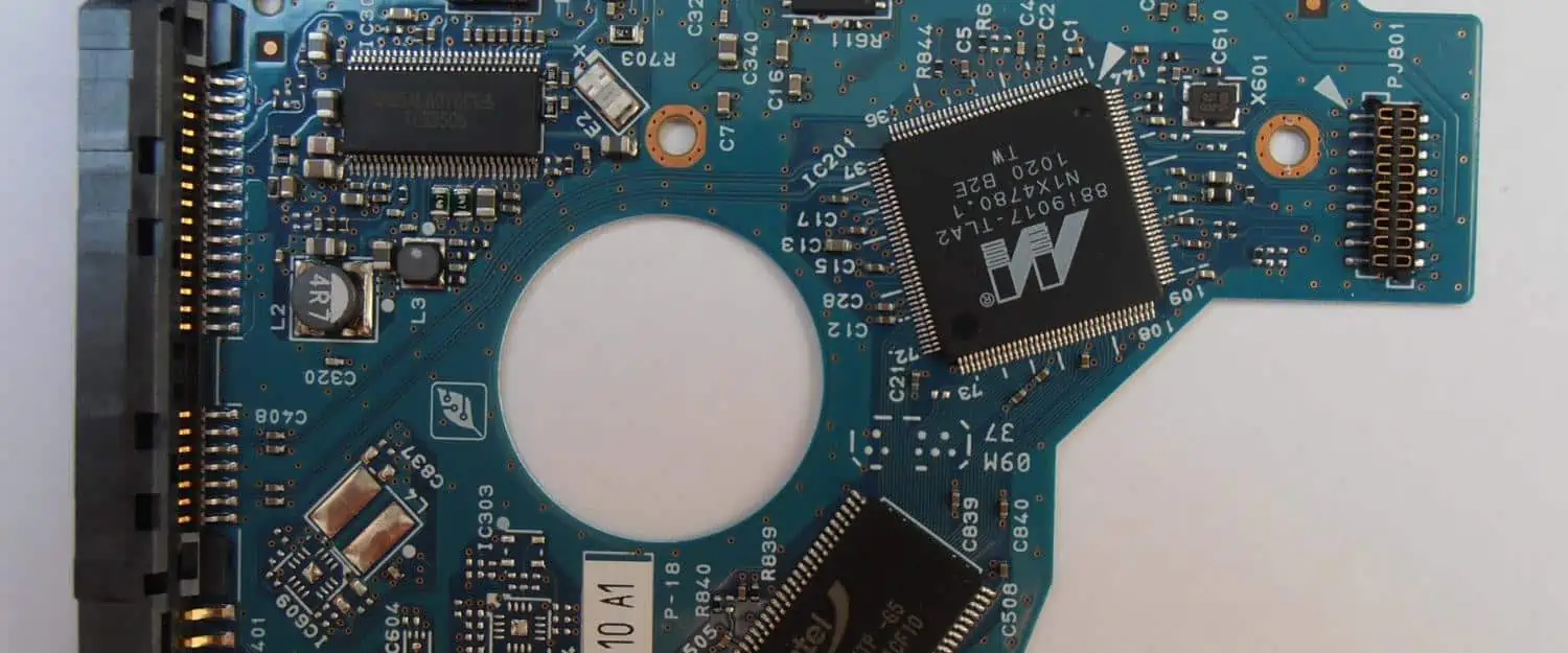
The main purpose is to control and coordinate all the components and operations within a hard drive. This includes powering drive motors, transferring data to/from the platters, communicating with the host computer, and monitoring drive health.
What happens if the PCB fails?
If the PCB suffers electrical damage or component failures, the drive can exhibit crashes, failed spin-ups, clicking noises, missing data, and other serious issues. The drive will be unusable until the board is replaced or repaired.
Can a damaged PCB be fixed?
It is sometimes possible to repair minor PCB failures by replacing individual chips or soldering damaged traces. But replacement boards may be needed for extensive damage. Proper equipment like a certified clean room is mandatory during PCB replacement to avoid platter damage.
What diagnostic tools are useful when troubleshooting PCBs?
Multimeters, current probes, and oscilloscopes help trace electrical issues on PCBs. Software tools like PC3000 can test component functionality. Thermal imaging can detect hot spots or failing elements. And data recovery software is useful if drive crashes or data loss occur.
How can hard drive PCB failures be prevented?
To maximize longevity, hard drives should be kept in proper operating temperatures without excessive vibration, shocks, moisture, or contaminants. Quality surge protectors prevent electrical damage. Maintaining current firmware and performing regular SMART drive self-tests also helps avoid issues.
Let me know if you would like me to elaborate on any part of this outline or change the structure in any way. I aimed for an organized, keyword-rich outline covering the key points, but can add more detail on any section needed. Just say the word!
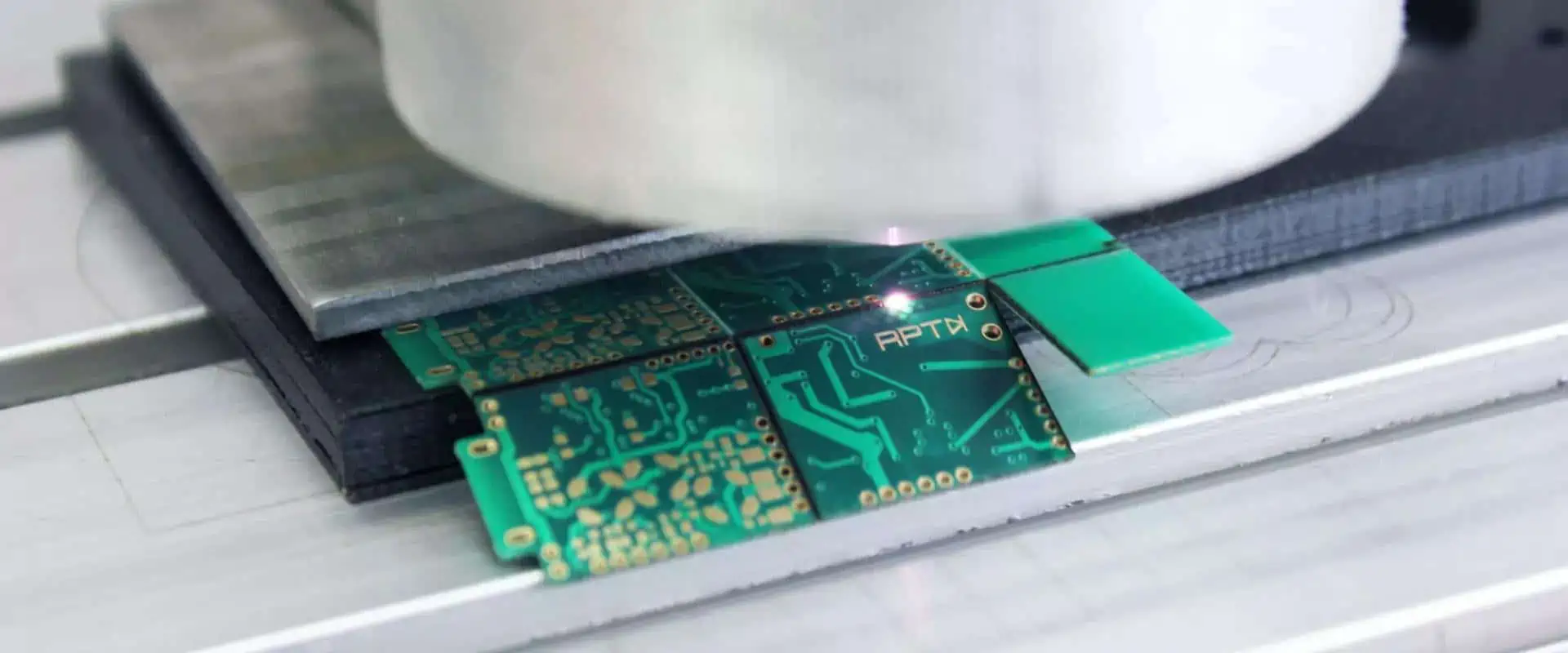
Printed circuit boards (PCBs) form the foundational backbone of electronics, but often need trimming to size before deployment in products. Cutting PCBs properly ensures precision standalone boards or panels ready for population.
This comprehensive guide covers PCB cutting methods, tools, materials, techniques and best practices in detail, including:
Cutting goals and challenges
Manual and automated cutting options
Blade selection, speeds and feeds
Fixturing, alignment and clamping
Quality and safety considerations
Hands-on step-by-step process
Follow along to learn essential PCB cutting skills for fabrication workflows or one-off prototyping!
Q: Can I use a handheld jigsaw or bandsaw to cut PCBs?
A: Yes, but the rapid coarse blades will likely fray laminate edges. Use fine finish blades and low feed rates instead for cleaner results.
Q: What are some signs of cutting issues or inadequate performance?
A: Watch for discoloration from overheating, jagged edges from dull tools, wandering paths, incomplete cuts, debris buildup on tools, and fraying on top or bottom surfaces.
Q: How do I cut complex board outlines or internal features?
A:CNC routers offer the best solution with customizable tool paths. For simple shapes, repeated straight cuts or nibbling can work but take more effort.
Q: Is it possible to hand cut PCB substrates over 2mm thickness?
A: Yes, but use extreme sharp carbide blades, scoring, tangential approaches to avoid cracking, and tiny increments to limit force required. Clamp boards tightly and mind hand safety.
Q: Can inadequate cutting damage PCB functionality?
A: Yes, fractured layers can disconnect traces, debris can short traces, heat can melt solder masks, and bending can crack components or joints leading to failure.
Conclusion
With the right manual or automated tools, techniques and quality checks, PCB boards can be cut to specification quickly while avoiding damage even on delicate high density boards. Carefully follow fundamental precision fixturing, controlled cutting and inspection methods to guarantee perfectly trimmed boards ready for installation and deployment.
Confidently master essential PCB board cutting skills using this reference to smoothly handle any custom modifications needed in your electronics workflow. Your expertise at cleanly shearing boards guarantees quality soldering, assembly and integration down the line!
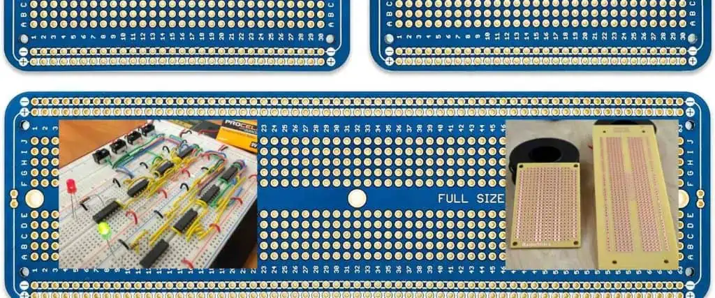
Prototype boards, also known as breadboards or solderless boards, are reusable circuit building tools used to prototype and test electronic designs during development. They allow creators to quickly connect and alter component configurations without any soldering.
This comprehensive guide will explain what prototype boards are, why they are useful, the different types available, and provide step-by-step instructions on how to effectively utilize them for electronics prototyping, including:
A prototype board or breadboard provides a convenient grid of interconnected spring clips and contact holes into which you can insert electronic components to construct a circuit, without any soldering involved.
Benefits
Here are the key advantages of using a prototype board:
Reusable – Allows repeated connecting and disconnecting of parts
Solderless – No soldering required for setting up circuits
Adjustable – Easy to alter component placements
Testable – Facilitates testing of circuit operation
Inexpensive – Affordable even for hobbyists
By letting you easily swap arrangements of integrated circuits, resistors, capacitors, inductors and more to form a circuit, prototype boards enable iterative electronic testing and troubleshooting.
Types of Prototype Boards
There are a few varieties of solderless breadboards or prototype boards:
1. Classic Breadboard
This is the most common type, providing connected horizontal rows of clip holes into which component leads or jumper wires can be inserted. The rows are divided in the center, with a positive and negative distribution bus line running vertically to supply power.
2. Mini Breadboard A smaller version of the classic breadboard with limited rows, portable for tiny projects.
3. Perfboard Instead of clips, perfboard offers an array of machined holes into which component leads can be hand-soldered. Allows more permanent assemblies.
4. Modular Breadboards For complex projects, modular breadboards can snap together to expand the prototyping area.
Inside a Breadboard
Looking inside a classic full-sized breadboard reveals how the spring-loaded clips provide electrical connectivity:
The black clips and holes are encased in clear plastic shells to provide insulation from neighboring rows. Metal nickel alloy leaves inside each clip provide electrical spring contact when component leads are inserted.
Rows marked with a – or + indicate connection leads out to the negative and positive bus lines on each side. This lets you easily distribute power supply voltages across the board.
Understanding these internal electrical connections is essential for planning your breadboard layouts!
Mounting Components on Breadboards
Components can be easily secured into a prototype board by plugging their lead wires or pins into the spring clip holes:
Insert Wires & Leads
1. Identify polarity indicators like +/- signs, long/short wire leads or pin positions. Align the positive and negative sides correctly.
2. Push leads/pins in firmly so they make contact with the metal leaves inside. But don’t over tighten or you may damage the contacts.
3. Ensure aligned rows to complete a connected circuit across adjacent clips. Misaligned rows will break connectivity.
4. Use jumper wires to bridge non-adjacent rows and route connections around as needed.
Mount ICs & Sockets
1. Outline the IC footprint by anchoring both ends in the same row.
2. Align Pin 1 markers correctly relative to internal rows.
3. Splay lateral pins outwards across adjacent contact clips for stability.
4. For sockets, mount them first, before plugging ICs into socket. Pressure fit for retention.
Here is a diagram showing insertion of common parts:
Correct positioning ensures reliable connectivity throughout your prototyped circuits!
Understanding basic prototype board connectivity allows you to transform schematics into physical layouts:
Tips
Start simple before increasing complexity
Verify alignments to schematics
Distribute power rails across rows
Bridge connections cleanly
Recheck contacts intermittently
Follow these prototyping best practices as you advance your circuits towards completion!
Complex Breadboard Projects
For intricate projects with higher component counts, utilize larger breadboards or modular linking for expanded capacity:
Considerations
Section functions into sub-units
Designate isolated power zones
Label rows and connections
Allow room for tweaking parts
Verify builds incrementally
Careful planning is key for keeping complex prototypes understandable and debuggable!
Breadboard Circuit Troubleshooting
Despite best efforts, prototypes may occasionally run into issues. Here is how to troubleshoot:
No Power
Check battery clips or power plugs
Test supply voltage presence on rails
Measure continuity out to rows
Short Circuits
Validate only intended connections
Eliminate solder fragments shorting clips
Prevent lead wires contacting closely
Erratic Operation
Redo all component insertions
Rule out cold joints or faulty parts
Reflow suspect solder points
Examine clips/ Sockets for wear debris
Methodically isolating the source from power input to individual sections will help identify any breadboard problems for correction.
Prototype Board Tips
Follow these handy guidelines for smoother prototyping sessions:
Part Insertion
Push wires and leads fully in without over bending them
Angle wider leads into offset holes for a snug fit
Use pliers to trim excess lead lengths
Stable Layouts
Heavier sections first, then build outward
Place adhesive foam under boards
Avoid lifting boards by protruding wires
Repeated Revisions
Preserve plugged layouts with photos
Label wire free ends by function
Clean clip debris before major changes
Once comfortable, prototype boards will accelerate your DIY electronics builds and learning!
Frequently Asked Questions
Q: How do I get a reliable connection to clips?
A: Check for shiny metal contact at lead insertion points. If inserts are loose, squeeze the surrounding plastic gently to increase grip, or change holes. Avoid wiggling inserted leads.
Q: My board has a manufacturing defect. Should I tear off the damaged section?
A: No, remove damaged portion with precision tools to avoid cracking cases open. Even small inner separations can impact electrical connectivity. Test for shorts after any invasive modification.
Q: Can prototype boards handle high voltages or power levels?
A: Most consumer boards are rated for under 25V and 500-1000mA max current only. For driving higher loads, research specialty breadboards or simply solder up finalized prototypes on perfboards/PCBs.
Q: Is it possible to burnout internal clips or connections through misuse?
A: Yes, repeated short circuits or extreme overheating can melt internal alloy contacts, cracking cases when expanding gas builds up. Avoid exceeding rating and rectify shorts quickly.
Q: Do breadboards ever need cleaning or maintenance?
A: Over time clip grip may loosen after frequent lead inserts/removals or environmental grime can accumulate. Use isopropyl alcohol with cotton buds to clean contact posts when necessary.
Prototype boards offer wonderful platforms for conveniently constructing, testing and modifying temporary electronic circuits with no soldering necessitated. Their spring contact holes allow you to securely host components in customized arrangements simply by plugging leads in to form desired connections.
Leverage breadboards to boost your hands-on learning when prototyping fresh designs from concept through maturation. The ability to rapidly alter layouts by just popping parts in and out of reusable boards accelerates iterative development, debugging, and functionality enhancement.
With practice, prototype boards become indispensable tools for giving creative outlet to electronic ideas as you advance from simple hookups towards ever more intricate projects! Just follow fundamental mounting guidelines, plan effective layouts for clean routing, and regularly validate contact integrity at insertion points.
So jump straight into prototyping your next electronic innovations on versatile breadboards before migrating successful verified builds onto permanent soldered PCBs or stripboards towards final deployment!
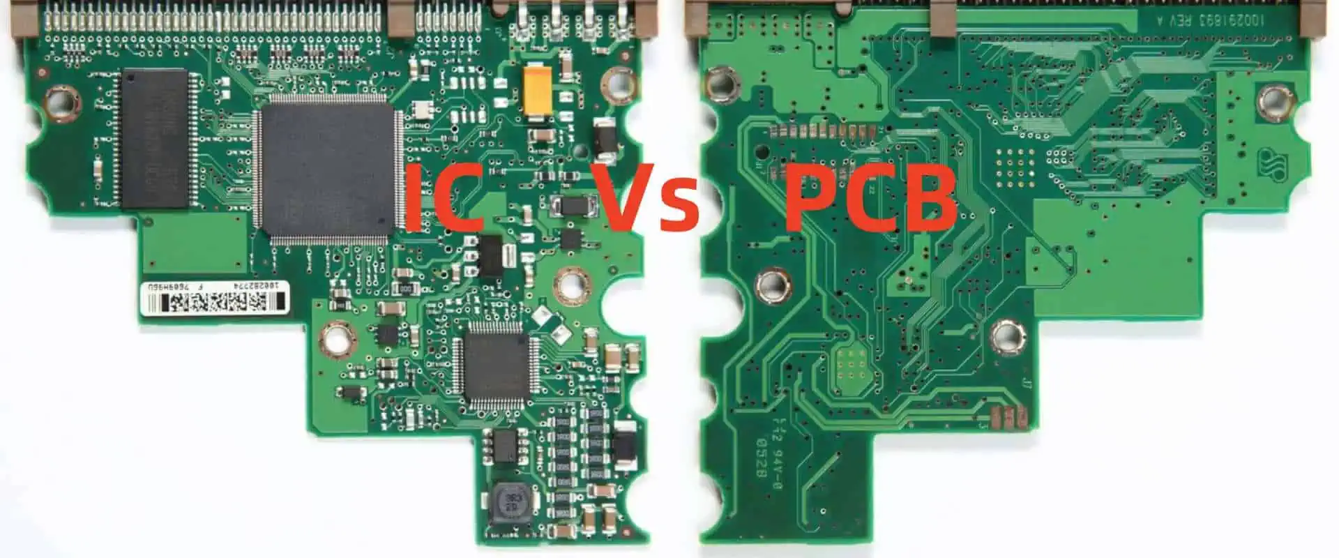
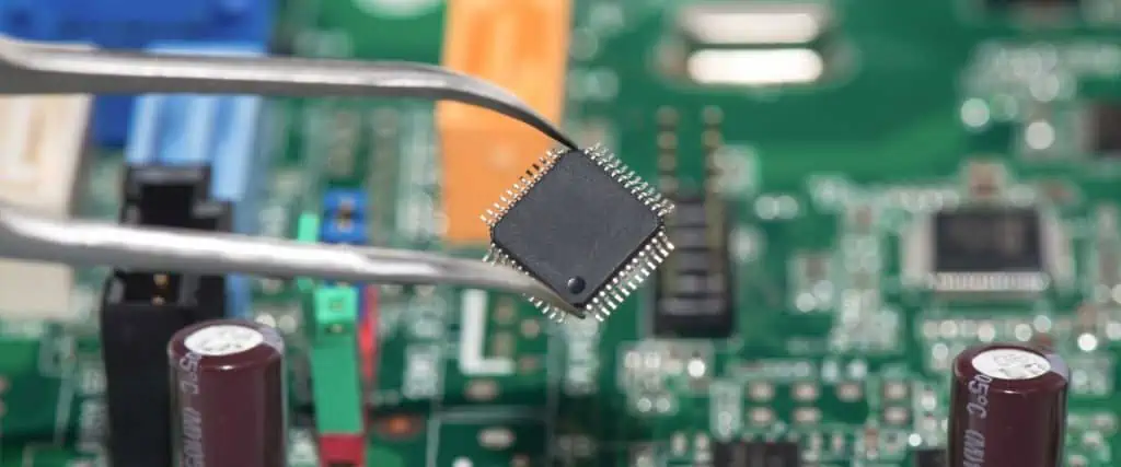
Integrated circuits (ICs) and printed circuit boards (PCBs) are both key components in modern electronics, but they serve different purposes. This article will explain what each one is, what they are made of, their role in an electronic system, and the key differences between the two.
What is an Integrated Circuit?
An integrated circuit, or IC, is a tiny silicon chip that can hold millions of microscopic electronic components like transistors, resistors, capacitors, and diodes. These components are etched onto the silicon through a fabrication process called photolithography.
ICs are essentially very complex electrical circuits with specific functions engraved on a single chip of semiconductor material. This “integrates” many components into one package instead of using separate, discrete components wired together on a circuit board.
Common types of ICs include:
Microprocessors – The central processing units (CPUs) that serve as the “brains” of a system, performing calculations and executing program instructions
Memory chips – Data storage chips like ROM, RAM, flash memory
Microcontrollers – Mini self-contained computers with processor cores, memory, and programmable input/output
Analog circuits – Chips that process continuous analog signals vs discrete digital data
ICs go by many names, including chip, microchip, silicon chip, semiconductor device, or just chip. Their small size packs tremendous functionality and computing power into integrated, miniaturized circuitry.
What is a Printed Circuit Board?
A printed circuit board (PCB) is a flat board made of insulating materials like FR-4 fiberglass onto which a “printed” conducting copper circuit is layered and affixed. The circuit wiring patterns are etched from copper sheets and provide electrical connections between mounted electronic components in an organized manner.
PCBs provide the mechanical framework to mount, connect, and integrate electronic components like ICs, resistors, capacitors, switches, connectors, batteries and more. They contain tiny copper tracks (wiring) leading to contact pads where component leads or connectors are soldered. Internal conductive layers and plated through holes connect tracks across layers.
In short, PCBs form the structural skeleton “platform” to assemble electronics hardware, while ICs power the functionality.
Semiconductors – Doped silicon with specific electric properties
Dielectrics – Insulating silicon dioxide layers
Conductors – Embedded polysilicon or aluminum metal interconnects
Passivation Glass – Protective top glass layer
This table summarizes the key material differences:
Materials
Printed Circuit Boards
Integrated Circuits
Base Board
Plastic composite like FR-4 fiberglass
Silicon wafer
Conductors
Copper metal traces
Polysilicon interconnects
Insulators
Non-conductive epoxy resin
Silicon dioxide
Coatings
ENIG over copper pads
Glassivation passivation layer
The base substrate, wiring, and insulation materials differ significantly between PCBs and ICs due to differences in their manufacturing processes and functionality.
Manufacturing Process Comparison
PCBs and ICs are produced in very different factories using unrelated fabrication processes:
PCB Manufacturing Steps
Design – PCB schematics and layouts are designed on EDA software
Cleaning – The substrate starts with an oil removal clean
Layer Stacking – Copper foil sheets are stacked up with substrate and prepreg
Alignment & Lamination – Sheets are aligned and glued with heat and pressure
Etching – Unwanted copper is chemically etched away
Photolithography – Photoresist patterns and etches further define traces
Plating & Coating – Exposed tracks are plated/coated with metals
This “backbone” architecture ties everything together into an integrated hardware system.
Key Differences Summary
Parameter
Integrated Circuits
Printed Circuit Boards
Definition
Miniaturized electronic computing components etched onto semiconductor material
Composite fiberglass boards providing structural base for circuit assembly
Composition
Silicon wafer substrate with embedded polysilicon interconnect circuitry
Fiberglass laminate with top and bottom layered copper foil conductors
Role
Provide core electronic functionality through precision integrated microcircuitry
Form mechanical framework to mount, connect, and support electronic components
Fabrication
Layer-by-layer deposition of doped silicon, dielectrics and conductors
Industrial processes of etching, coating, and lithography to shape substrate layers
End Use
Installed onto PCBs for functional deployment
Host ICs and other electronics parts integrated through copper wiring traces
In summary, ICs bring the complex electronic functionality that drives computation, while PCBs structurally support integration of these parts into complete working systems.
Here are answers to some common questions about ICs versus PCBs:
Q: Can an IC work without being mounted on a PCB?
A: No, ICs by themselves have no way to interconnect or physically mount inside a system. They must be appropriately placed and soldered onto PCBs to connect their input/output pins to copper wiring traces.
Q: Does a PCB have any function if no ICs are installed?
A: A plain PCB with only connectors brings little functionality. The ICs drive core digital processing, computation, memory, logic, and control capabilities to create an intelligent system.
Q: Which came first historically – PCBs or ICs?
A: PCBs originated from 1950s military electronics, while the first ICs emerged in 1961. So PCBs initially carried more discrete components until higher density ICs slowly got integrated over the 1960s and 70s.
Q: Can you implement an electronic product with just ICs or just a PCB?
A: No. All modern electronics require both complementary components. ICs provide function while PCBs enable integration, similar to organs and bones in the body.
Q: How are PCBs and ICs interconnected?
A: ICs packaging has metallic leads that get soldered onto matching copper contact pads on a PCB. This electrically and mechanically bonds them together through conductive solder alloy, enabling circuit connections.
Conclusion
Integrated circuits and printed circuit boards work hand-in-hand to enable all modern electronics. ICs integrate complex digital processing circuitry onto tiny silicon chips, which get structurally mounted onto the interconnect copper wiring traces of PCBs.
Understanding their distinct compositions, manufacturing processes, and functional roles is key to designing and assembling any electronic hardware product. Their synergistic partnership merges electronic functionality with an integration backbone into one powerful package.
So next time you look at an electronic device, recognize the critical symbiosis between precision integrated circuits energizing high-function silicon chips at the core, seamlessly enabling system integration through their attachment to flexible printed circuit boards!
Industrial monitoring instrumentation (IMI) sensors play a crucial role in measuring and controlling processes across various industries. This article provides an overview of key IMI sensor types, applications, selection considerations, and frequently asked questions.
Temperature Sensors
Temperature measurement and control is critical for product quality, system performance, and safety. Common temperature sensor types include:
Thermocouples
Thermocouples contain two conductors made of different metals fused at one end. This junction produces a small voltage relative to temperature:
Inexpensive compared to other sensors
Wide temperature ranges up to 2300°C
Low-cost options for fairly accurate temperature measurement
Available in different types—K, J, T, E, R, S, B, N
Resistance Temperature Detectors (RTDs)
RTDs contain a wire coil or film made of metals like platinum, copper or nickel. As temperature increases, electrical resistance increases linearly:
High accuracy with tight tolerance capability
Better repeatability and stability than thermocouples
Range capabilities from -200 °C to 850 °C
Common RTD types—Pt100, Pt1000, Ni120, Cu10
Thermistors
Thermistors contain semiconductor ceramics that alter resistance according to temperature fluctuation:
Inexpensive
Fast response times
Common as inrush current limiters and self-regulating heating elements
Can have high non-linearity requiring linearization
Table comparing different temperature sensor attributes:
Gas monitoring is vital for safety, emissions control, and process optimization. Instruments include:
Infrared Gas Sensors
Leverage infrared light absorption characteristics of target gases:
Available for most common toxic gases
Typically very sensitive and stable
Can have interference issues in dirty environments
Electrochemical Gas Sensors
Use electrode reactions to quantitatively indicate target gases:
Offer ppm sensitivity levels
Simple and inexpensive
Prone to poisoning/contamination failure
Metal Oxide Semiconductor (MOS) Sensors
Alter conductive states based on reactions with oxidizing/reducing gases:
Respond to wide variety of reactive gases
Operate well at high temperatures
Lack specificity between gas types
Lifespans limited by operational duty cycles
Photoionization Detectors (PID)
Ionize chemical gases using ultraviolet light for detection:
Respond to diverse VOCs
Sub-ppm sensitivity
Unable to differentiate specific compounds
Require periodic UV lamp replacement
Catalytic Bead Sensors
Detect combustible gases via combustion on electrically heated pellistors:
Wide rangeability can reach 100% LEL
Low purchase and operating costs
Lack specificity between gas types
Table summarizing instrumentation for gas detection:
Sensor
Range
Accuracy
Price
Selectivity
Infrared
0-100% LEL
Very High
$$
Excellent
Electrochemical
ppm levels
High
$
Good
Metal Oxide
ppm levels
Medium
$
Poor
Photoionization
ppb-ppm
High
$$
Medium
Catalytic Bead
0-100% LEL
Medium
$
Poor
Process Analytical Instruments
Process analyzers provide real-time quantification of liquid/gas chemistries:
PH Instrumentation
PH measurement is critical for monitoring water quality, reactor processes, and biological processes. Options include:
Electrochemical electrodes – common for inline industrial measurement
Litmus paper – inexpensive spot sampling
Digital benchtop/handheld meters – laboratory analysis
PH control instrumentation includes chemical metering pumps, solenoid valves, and databases of automated dosing control algorithms.
Conductivity Measurement
Conductivity cells quantify ion concentrations within process liquids. This can identify:
Impurities in water feeds
Chemical reaction progression
Alkalinity and other water chemistry
Typical instrumentation incorporates contactless toroidal sensors or diagnostic tables for identifying specific chemical components based on conductivity.
Gas Chromatographs
Gas chromatographs utilize separation columns and compositional analysis to identify gas mixtures. Applications involve:
Natural gas, fuel, and feedstock purity
Quantifying levels of contaminants
Monitoring chemical reaction progress
Chromatographs offer excellent analytical precision but require skilled personnel for calibration and data interpretation.
Spectrophotometers
Spectrophotometric analyzers pass specific wavelengths of light through samples to quantify absorption characteristics. This identifies:
What are the different kinds of transmitters for IMI sensors?
Common transmitter outputs include 4-20 mA analog, HART digital communication, WirelessHART, Foundation Fieldbus, Profibus PA, and modular plug-in universal designs. This provides connectivity to control systems like PLCs and DCS platforms.
How do you install RTD temperature sensors?
RTD sensors require precise immersion depth control and thermal grease/compound to ensure proper heat transfer contact. 3 or 4-wire configurations compensate for lead resistance. Match sheath materials to environmental media compatibility.
How do I prevent corrosion failure in pressure sensors?
Choose compatible wetted parts materials for process fluids. Use chemical seals/diaphragms. Control fluid velocity/turbulence at sensor connections. Avoid fluid ingress through proper mounting orientation. Consider corrosion resistant coatings and surface treatments.
What flow sensors work with dirty liquids?
Differential pressure instruments tolerate considerable solids contamination when properly designed. Magnetic flow meters lack flow obstructions enabling particulate passage. Coriolis meters dynamically flex flow tubes to prevent accumulation when measuring slurries.
How often should gas detectors be calibrated?
Electrochemical and infrared sensor performance drifts over 6-12 month intervals depending on environmental factors and pollutant exposure. Recommended gas detector calibration frequency ranges from monthly to annually. Always adhere to manufacturer guidance for recalibration and replacement intervals.
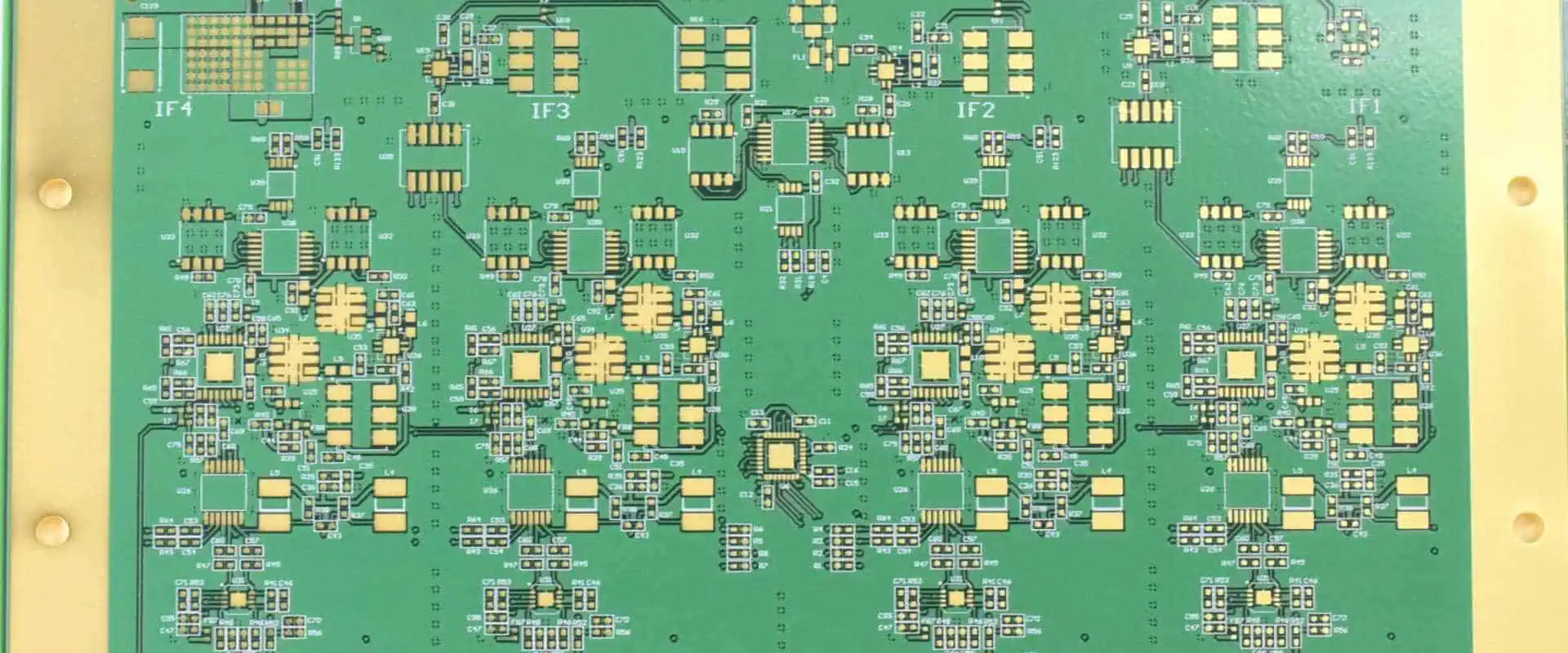
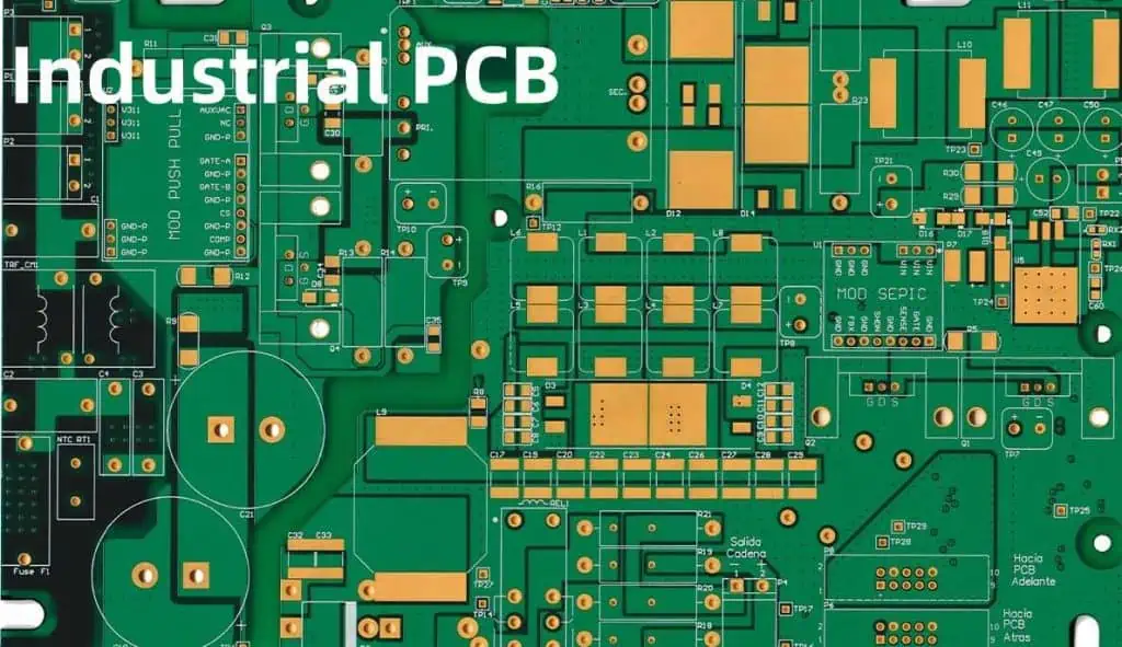
Industrial printed circuit boards (PCBs) refer to boards designed to operate reliably in demanding environmental conditions for extended time periods, usually 5-10+ years. They enable core functions for products used in sectors like transportation, energy, automation, aerospace and defense.
Unlike commercial grade boards, industrial PCBs face punishing temperature swings, shock, vibration, humidity and other challenges. They require rigorous design, component selection and testing well beyond typical electronics. In this guide, we explain what defines industrial PCBs and overview key design and manufacturing standards driving longer lasting, rugged boards.
Defining Industrial PCBs
Industrial PCBs differentiate on:
Operating Environments – Made for extreme industrial settings with wider temperature (-40°C to 105+°C), shock/vibration, humidity and other environmental demands.
Lifespan – Designed for high reliability over long product field life, often 10-15+ years of near continuous operations.
Criticality – High availability, functionality and safety criticality if the PCB fails. Whole industrial systems may rely on them.
Some examples of electronics using specially designed industrial class PCBs include:
Ruggedness, extended lifespan and high reliability distinguish industrial PCBs even though they may resemble commercial boards upon visual inspection. Their unique constraints lead to various design and manufacturing rules.
Engineers designing industrial printed circuit boards face various international standards prescribing construction methods, documentation models, risk analysis techniques, testing procedures and key metrics to achieve longer field life over temperature extremes, vibrations and fast transients.
Some of the major standards include:
IPC Class 3
Issued under IPC-2221 standards, it covers generic performance requirements for industrial electronics printed boards especially related to:
Temperature cycling (-65°C to 150°C)
Vibration (10-500Hz at 10G+)
Mechanical shock of 100-1500G
Moisture resistance
Other environmental stresses
Additionally covers recommended test methods, quality conformance criteria and inspection details useful for qualifying Class 3 boards. It represents a minimum level for most industrial applications.
IPC-6012 Automotive Electronics
Includes performance standards tailored for automotive/transportation use cases covering details like:
Temperature ranges (-40°C to +125°C )
Rapid humidity transitions
Vibration profiles
Test schedules
Inspection criteria
Qualification maintenance
Contains Class 1, 2, 3 acceptance levels (Class 3 most demanding)
IPC-A-610 Acceptability Standard
Visual defect criteria focused on workmanship, component orientation, soldering, part types and surface finishes. Used globally across PCB types to determine quality through manufacturing and acceptance inspection. All boards should pass IPC-A-610 for ship readiness.
Of note for industrial boards are temperature/humidity cycling, mixed flowing gas corrosion testing and chemical resistance outlined.
UL 796 Standard for Printed-Wiring Boards
Underwriters Laboratory standard including various flame resistance, temperature indexing tests, electrical testing and constructions methods for boards.
Special UL 796 File Number recognition requires passing a range of safety focused design evaluations applicable to boards used in the UL safety certification ecosystem. Useful for boards used in end-products seeking UL listing especially for power electronics.
Industrial PCB Materials and Constructions
To withstand higher stress, industrial PCBs utilize additional materials and stackup methods:
Design is crucial for reliable functionality under demanding conditions:
Simulation Early – Extensive electrical, thermal, vibration modeling using tools like Ansys or Comsol to predict response and resonances. Spot problems ahead of building prototypes pcb.
Derating Rules – Component derating guidelines lowering actual operating values below datasheet absolute maximums for voltage, current and power. Provides margin against parameter drift and lifespan reduction.
Redundancy – Extra backup pathways, traces, connections with automated failover capability. Prevents single points of failure.
Layout Methods – Thermal management techniques, stitching vias, edge control structures and wide, thick conductors to handle vibration, currents.
DFMx Analysis – Rigorous design analysis checks for manufacturability issues around thermal relief connections, trace widths, annular rings and more.
Standards Validation – Testing conformity with defense standards like MIL-PRF-31032 or those above helps qualify designs.
Getting board layout right from the start avoids costly re-spins later so taking the time to simulate, analyze and standard-proof industrial PCB designs is well worth it.
Producing industrial PCBs uses tighter process controls, auditing and qualification procedures than commercial boards:
Software – MES, ERP, MRP help coordinate workflow, Machine interfaces aid automated optical inspection and test
Fab – Cleanrooms, 6 sigma process controls on 35+ fabrication steps including pattern plating.
Test – ICT finds shorts and opens. Flying probe checks nodes. AOI inspects defects. X-ray confirms inner layer detail.
QA – Full traceability on materials and processes. Conflict minerals reporting required. Factory audited to AS9100, ISO 9001
Qualification – IPC Class 3 certification, UL E-file safety approval after verification testing during new product introduction and then sustained through periodic re-qualification
Personnel – Operators undergo certified training on accepting boards to IPC-A-610 visual standards reliably
Data Packs – Full archive packs for each board with photomicrographs, electrical test results,Corrective action reports from any issues detected during manufacturing or test
This combination of precision digital manufacturing technology paired with quality framework helps yield the reliable, long lasting circuit boards needed in industrial situations.
Choosing an Industrial PCB Partner
Given the unique demands of industrial PCBs, partner selection matters greatly:
Look for
Years of experience specifically with industrial customers
Wide material expertise like ceramic, IMS, flex-rigid and metal core PCBs
Design for Excellence services aiding product development
Staff engineers that can validate layouts to standards
Global quality certifications – ISO, AS9100
Ask About
Handling of proprietary customer data and red team reviews
DFM optimization methods and GERBER analysis
Standard testing and inspection processes
Qualification reports provided
Inventory and obsolescence management programs
Counterfeit part avoidance controls
This best equips product teams to accelerate robust, compliant printed circuit board designs optimized to survive longterm in the real world conditions faced.
Conclusion
Industrial electronics have special PCB reliability requirements well beyond commercial boards to perform properly for years across extreme environments and safety critical applications.
By designing to rigorous standards upfront through simulation, analysis, derating and redundancy while choosing a tightly controlled, certified PCB factory, companies can meet their customers’ expectations in the harshest use cases. The specialized materials, testing and qualification processes for industrial PCBs delivers confidence for successful field deployment.
Frequently Asked Questions
What are some example applications using industrial class PCBs?
Typical applications leveraging industrial printed circuit boards include transportation power systems, factory automation controllers, energy management products, remote telemetry units, military vehicle computing, aerospace avionics, downhole drilling tools, naval systems and similar electronics where high reliability over 5-15+ years is necessary.
How are industrial PCBs different than commercial PCBs?
Industrial PCBs differentiate by:
Supporting wider operating temperatures (-65°C to +150°C)
Longer field deployment lifetimes (10-20 years)
Required survival through harsh vibration, shock, moisture conditions
High availability and uptime (>99%)
Rigorous product testing and qualification
Precision manufacturing process controls
Traceability documentation Which exceeds commercial PCB environmental and lifespan demands.
What are some ways engineers design industrial PCB layouts differently?
Design techniques used for industrial printed circuit boards include:
Component derating below absolute maximum levels
Thermal simulation using finite element models
Redundant connections and pathways
Vibration damping edge mount connectors
Conformal coating for moisture protection
Thicker power and ground traces
Double sided boards to withstand shock
Extensive DFM analysis before release
Why is FR-4 still commonly used if industrial PCBs face extreme temperatures?
While special substrates like polyimides and ceramics handle wider temperature swings, FR-4 laminates have evolved “high Tg” versions usable to 150°C+ along with lower cost and better fabricator familiarity. So FR-4 remains an option for many industrial applications not hitting extreme temps.
What certifications should we look for in an industrial PCB manufacturer?
Key quality certifications to require from a factory producing printed circuit boards destined for industrial products include:
ISO-9001-2015 – Quality management systems
AS-9100D/EN9100 – Aerospace standard with strict guidelines
ANSI/ESD S20.20 – Control of electronics ESD hazards
ISO 14001:2015 Environmental Management
IATF 16949 – Automotive quality management
ITAR registration – Required for defense/aerospace PCBs
Designing a printed circuit board (PCB) goes beyond simply connecting components—it’s about engineering a product that is reliable, manufacturable, and compliant with industry best practices. This is where IPC standards play a crucial role.
As the most widely recognized guidelines in electronics manufacturing, IPC standards define the design, fabrication, and assembly requirements that ensure PCBs perform consistently across industries—from consumer electronics to aerospace and defense. These standards influence everything from trace width and spacing to thermal management and material selection, helping designers avoid costly errors and production delays.
The primary objective of IPC standards is to guarantee safety, reliability, and manufacturability in electronic products. Whether you’re developing medical devices, automotive systems, or industrial equipment, adhering to IPC guidelines helps meet regulatory requirements, reduce defects, and improve overall product quality.
Understanding IPC Standards for PCB Design
IPC, formerly known as the Institute for Printed Circuits and now as the Association Connecting Electronics Industries, is a global trade association that sets the standards for the electronic interconnect industry. IPC Standards for PCB Design are a set of guidelines and requirements that ensure consistency, quality, and reliability in PCB production across the industry.
Why IPC Standards Matter in PCB Design
IPC Standards play a crucial role in the PCB industry for several reasons:
Quality Assurance: They provide a benchmark for quality, ensuring that PCBs meet specific performance and reliability criteria.
Consistency: Standards enable consistency across different manufacturers and suppliers, facilitating easier collaboration and interoperability.
Cost Reduction: By following standardized practices, manufacturers can reduce errors, rework, and waste, ultimately lowering production costs.
Innovation: Standards provide a foundation upon which new technologies and design techniques can be built and integrated.
Global Communication: IPC Standards serve as a common language for the industry, improving communication between designers, manufacturers, and customers worldwide.
Powered By EmbedPress
Key IPC Standards for PCB Design
Let’s explore some of the most important IPC Standards that directly impact PCB design:
IPC-2220 Series: Design Standards
The IPC-2220 series is fundamental to PCB design, covering various aspects of the design process.
IPC-2221: Generic Standard on Printed Board Design
This standard provides general requirements for the design of printed boards and forms the foundation for other design standards in the series.
Key aspects covered:
Material selection
Electrical and mechanical considerations
Thermal management
Design for manufacturability (DFM)
Documentation requirements
IPC-2222: Sectional Design Standard for Rigid Organic Printed Boards
This standard focuses specifically on the design of rigid organic printed boards, building upon the general requirements outlined in IPC-2221.
Areas of focus:
Layer stackup considerations
Conductor spacing and width requirements
Via and hole design rules
Soldermask and silkscreen guidelines
IPC-2223: Sectional Design Standard for Flexible Printed Boards
For designers working with flexible PCBs, this standard provides specific guidelines and requirements.
Key topics:
Flexible material selection and properties
Bend radius considerations
Dynamic flexing requirements
Adhesive selection and application
IPC-2226: Sectional Design Standard for High Density Interconnect (HDI) Printed Boards
As PCB designs become increasingly complex and miniaturized, HDI technology has become crucial. This standard addresses the specific requirements for HDI PCB design.
Important aspects:
Microvia design and fabrication
Fine line and space requirements
Stacked and staggered via structures
Laser drilling considerations
IPC-6010 Series: Performance Specifications
While the IPC-2220 series focuses on design, the IPC-6010 series sets the performance specifications for finished PCBs.
IPC-6011: Generic Performance Specification for Printed Boards
This standard establishes the general performance requirements for PCBs, regardless of their specific type or application.
Key areas covered:
Electrical performance criteria
Mechanical integrity requirements
Environmental resistance specifications
Marking and traceability guidelines
IPC-6012: Qualification and Performance Specification for Rigid Printed Boards
Hardware Layout
Building on IPC-6011, this standard provides specific performance requirements for rigid PCBs.
Important aspects:
Dimensional and physical property requirements
Solderability and resistance to soldering heat
Thermal stress resistance
Cleanliness requirements
IPC-6013: Qualification and Performance Specification for Flexible Printed Boards
For flexible PCBs, this standard outlines the specific performance criteria that must be met.
Key topics:
Flexibility and endurance requirements
Adhesion strength specifications
Dimensional stability under various conditions
Specialized testing procedures for flexible circuits
IPC-7351: Generic Requirements for Surface Mount Design and Land Pattern Standard
This standard is crucial for designers working with surface mount technology (SMT), which is prevalent in modern PCB designs.
Understanding IPC Standards is one thing, but implementing them effectively in your PCB design workflow is another. Here are some best practices for incorporating IPC Standards into your design process:
1. Education and Training
Ensure that your design team is well-versed in the relevant IPC Standards:
Conduct regular training sessions on IPC Standards updates
Encourage designers to obtain IPC certifications
Maintain a library of IPC Standards documentation for easy reference
2. Design Rule Implementation
Integrate IPC Standards into your design rules within your PCB design software:
Set up design rule checks (DRCs) based on IPC specifications
Create custom design rule sets for different product classes (Class 1, 2, or 3)
Regularly update these rules as standards evolve
3. Component Library Management
Maintain a component library that adheres to IPC Standards:
Use IPC-compliant footprints for surface mount components
Include IPC-recommended land patterns in your library
Regularly audit and update your component library to ensure ongoing compliance
4. Design for Manufacturability (DFM)
Incorporate DFM principles based on IPC Standards:
Follow IPC guidelines for conductor spacing, width, and clearances
Adhere to IPC recommendations for via and hole design
Consider IPC-defined material properties in your stackup design
5. Documentation and Specifications
Ensure your design documentation aligns with IPC Standards:
Use IPC-specified drawing formats and symbols
Include IPC-recommended fabrication and assembly notes
Clearly specify which IPC Standards and classes apply to your design
6. Collaboration with Manufacturers
Work closely with your PCB manufacturers to ensure IPC Standard compliance:
Communicate which IPC Standards are applicable to your design
Request IPC-compliant manufacturing processes
Discuss any deviations from IPC Standards and their potential impacts
Use IPC-defined test methods for electrical and mechanical verification
Adhere to IPC cleanliness and inspection criteria
Maintain records of compliance and any non-conformances
Advanced Topics in IPC Standards for PCB Design
As PCB technology continues to advance, IPC Standards evolve to address new challenges and opportunities. Let’s explore some advanced topics covered by IPC Standards:
High-Speed and High-Frequency Design
With the increasing prevalence of high-speed digital and RF applications, IPC has developed standards to address these specialized design requirements:
IPC-2251: Design Guide for the Packaging of High Speed Electronic Circuits
This guide provides recommendations for designing high-speed PCBs, covering topics such as:
Impedance control techniques
Signal integrity considerations
Power distribution network (PDN) design
EMI/EMC mitigation strategies
IPC-2141: Design Guide for High-Speed Controlled Impedance Circuit Boards
Focused specifically on controlled impedance design, this guide covers:
Test and verification methods for controlled impedance
Embedded Components Technology
As PCB designs become more compact and integrated, embedded component technology is gaining traction. IPC has responded with standards addressing this emerging field:
IPC-7092: Design and Assembly Process Implementation for Embedded Components
This standard provides guidelines for designing PCBs with embedded passive and active components, covering:
Design considerations for embedding components
Material selection for embedded component PCBs
Manufacturing process requirements
Reliability and testing considerations
Additive Manufacturing for PCBs
3D printing technology is making inroads into PCB manufacturing, prompting the development of new standards:
IPC-4921: Requirements for Printed Electronics Base Materials
While not specific to additive manufacturing, this standard lays the groundwork for materials used in emerging PCB fabrication technologies, including:
Material properties for printed electronics
Test methods for printed electronic materials
Performance requirements for various applications
The Future of IPC Standards for PCB Design
As technology continues to evolve at a rapid pace, IPC Standards must adapt to remain relevant and effective. Here are some areas where we can expect to see developments in IPC Standards for PCB Design:
1. Internet of Things (IoT) and Wearable Devices
The proliferation of IoT and wearable devices presents new challenges in terms of miniaturization, flexibility, and durability. Future IPC Standards may address:
Integration of sensors and antennas in PCB designs
Durability standards for wearable electronics
2. 5G and Beyond
As 5G technology rolls out and research into 6G begins, PCB designs for high-frequency applications will become increasingly important. Future standards may focus on:
The integration of AI and ML capabilities into PCB designs may lead to new standards addressing:
Design considerations for AI accelerator chips
Thermal management for high-performance computing PCBs
Power distribution for AI-enabled devices
4. Sustainability and Environmental Considerations
As environmental concerns become more pressing, future IPC Standards may place greater emphasis on:
Design for recyclability and circular economy principles
Use of sustainable and biodegradable materials in PCB manufacturing
Energy efficiency in PCB design and production
5. Quantum Computing
As quantum computing technology advances, specialized PCB designs will be required. Future IPC Standards may need to address:
Ultra-low temperature PCB designs for quantum circuits
Specialized materials for quantum-compatible PCBs
Unique testing and verification procedures for quantum PCBs
Challenges in Implementing IPC Standards for PCB Design
While IPC Standards provide numerous benefits, their implementation can present challenges for PCB designers and manufacturers:
1. Keeping Up with Revisions
IPC Standards are regularly updated to reflect technological advancements and industry needs. Staying current with these revisions can be challenging:
Allocate resources for ongoing education and training
Implement a system for tracking and implementing standard updates
Regularly review and update internal design guidelines
2. Balancing Standards with Innovation
Sometimes, cutting-edge designs may push the boundaries of existing standards:
Develop processes for evaluating and justifying deviations from standards
Engage with IPC committees to provide feedback on emerging design needs
Document and share experiences to contribute to future standard revisions
3. Cost of Compliance
Adhering to IPC Standards can sometimes increase design and manufacturing costs:
Conduct cost-benefit analyses to justify standard implementation
Look for opportunities to streamline processes through standardization
Consider the long-term benefits of improved quality and reliability
4. Global Variations
While IPC Standards are widely recognized, some regions may have additional or differing requirements:
Be aware of regional variations in standards and regulations
Develop flexible design processes that can adapt to different requirements
Foster communication between global design teams to share best practices
5. Complexity in Multi-Board Systems
Modern electronic products often involve multiple interconnected PCBs, which can complicate standards compliance:
Develop system-level design guidelines that incorporate IPC Standards
Consider the interplay between different board types (rigid, flex, rigid-flex) in a single system
Implement comprehensive testing procedures for multi-board assemblies
Conclusion: The Vital Role of IPC Standards in PCB Design
IPC Standards for PCB Design play a crucial role in ensuring the reliability, performance, and interoperability of electronic devices in our increasingly connected world. By providing a common framework for design, manufacturing, and quality assurance, these standards enable the electronics industry to meet the ever-growing demands for smaller, faster, and more complex devices.
As we’ve explored in this comprehensive guide, IPC Standards cover a wide range of topics, from basic design principles to advanced technologies like high-speed design and embedded components. By implementing these standards in your PCB design workflow, you can:
Improve the quality and reliability of your PCB designs
Enhance communication and collaboration with manufacturers and suppliers
Reduce costs associated with errors, rework, and production issues
Stay at the forefront of technological advancements in the PCB industry
However, it’s important to remember that IPC Standards are not static. They continue to evolve alongside technological advancements, addressing new challenges and opportunities in areas such as IoT, 5G, AI, and beyond. As a PCB designer or manufacturer, staying informed about these evolving standards and actively participating in their development is key to remaining competitive in the industry.
Ultimately, the judicious application of IPC Standards for PCB Design is not just about compliance – it’s about creating better, more reliable electronic products that can meet the demands of today’s technology-driven world. By embracing these standards and integrating them into your design philosophy, you can ensure that your PCB designs are not just meeting the minimum requirements, but are positioned to excel in performance, reliability, and manufacturability.
As we look to the future, the role of IPC Standards in PCB design will only grow in importance. By staying committed to these standards and contributing to their ongoing development, the PCB design community can continue to push the boundaries of what’s possible in electronics, driving innovation and shaping the technologies that will define our future.
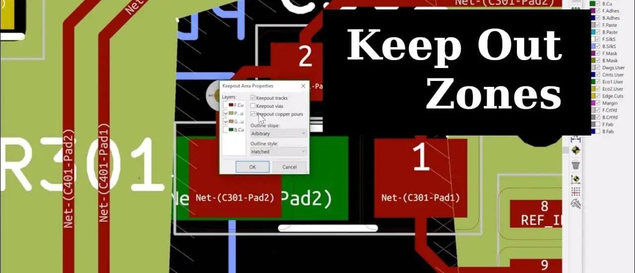
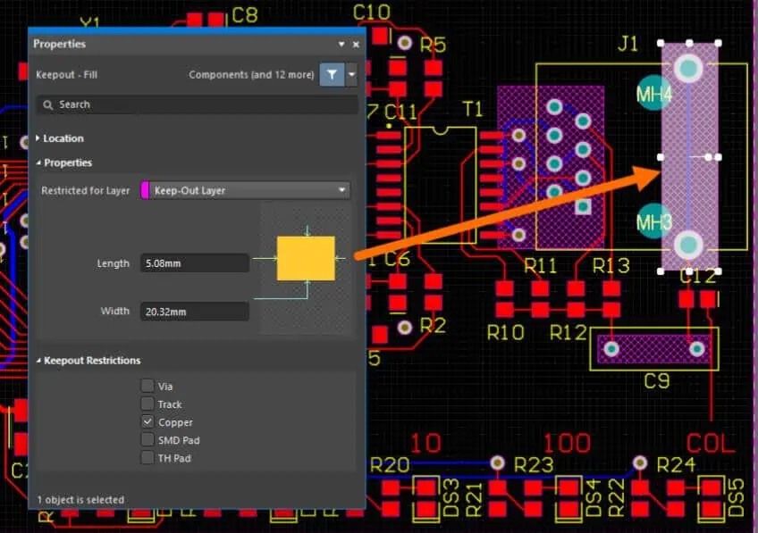
Route keepin and keepout are critical concepts in printed circuit board (PCB) design that refer to deliberately routing traces through or avoiding certain regions to meet layout guidelines and electrical requirements.
Route keepin defines areas where the PCB router must pass signal traces to force connectivity with components placed in that zone.
Route keepout conversely defines excluded regions that traces must avoid routing through to prevent interference or maintain spacing from nearby components.
Understanding keepin and keepout methodologies is essential to optimizing PCB routing and minimizing signal quality issues or fabrication defects.
Makes routing pass through periodic vias to stitch together different layer planes. Maintains proper return paths.
Faraday Cage Keepin
Routes traces through shielding cages around noise sensitive circuitry to maintain isolation.
Mechanical Outline Keepin
Routes critical traces along the physical PCB extents to enable edge mount connectors.
Types of Route Keepout
Various key route keepout regions also exist:
Silkscreen Keepout
Avoids placing traces under annotations to prevent visibility issues after fabrication.
Copper Pour Keepout
Prevents traces from entering copper fill areas to avoid accidental bridging due to etching defects.
Electrical Clearance Keepout
Ensures separation between traces and adjacent pads/traces meets target clearance rules to prevent short circuits.
Mechanical Drill Keepout
Keeps traces clearing away from mechanically drilled PCB holes to account for potential drill wandering during fabrication.
Test Points Keepout
Allows space for temporary test point accesses around points of interest for debug probing without blocking trace routability.
Implementing Keepin and Keepout in PCB Layout
PCB layout tools provide both manual and automated methods to assign route keepin and keepout:
Manual Assignment
The designer manually draws required keepin/keepout shapes and configures rules forcing or blocking traces from entering each area. Allows precision control but can be time consuming.
Component-Driven Automation
Software automation dynamically generates mandated trace access or exclusion areas based on placed component pin locations, pad geometry, and electrical settings like net classes. More efficient but with less customization.
Manufacturing-Driven Standards
Many fabricators provide standard design rule check (DRC) constraint files that designer tools leverage to auto-assign generic keepin/keepout regions. Facilitates ease-of-fabrication but with conservative assumptions.
Benefits of Implementing Thoughtful Keepin and Keepout
Intelligent use of route keepin and keepout delivers major PCB optimization including:
1. Ensures Critical Trace Connectivity
Forcing traces through certain areas guarantees nodes that must be electrically tied together connect during routing without reliance on designer effort to pre-route.
2. Reduces Signal Integrity Issues
Separating sensitive nets using pin/trace exclusion regions enables cleaner routing with less undesired coupling that degrades signal performance.
3. Optimizes Manufacturability
Guiding traces to required locations and away from high-risk zones proactively mitigates potential fabrication defects through prevention.
4. Facilitates Debugging
Strategic channel creation permits test probes access during bring-up labs while isolation barriers prevent probe grounding issues.
Impact of Keepin/Keepout Misconfiguration Hazards
While powerful capabilities, incorrect keepin/keepout implementations risk major consequences:
Excessive Route Blockage
Over-constraining areas that traces must avoid can block all viable routing paths resulting in incomplete trace connections.
Signal Performance Degradation
Allowing sensitive traces to occupy noise-coupled regions without proper isolation degrades signal spectral purity, eye diagrams, jitter, and bit error rates.
Fabrication Defect Generation
Permitting traces into zones with insufficient electrical or mechanical spacing guarantees at least localized short circuits and potential panel scrapping.
Test Access Limitations
Lack of test point regions can prevent affirming critical internal nodes leading to extensive debug efforts when integration issues emerge.
PCB Examples Using Effective Keepin and Keepout
Several case study examples highlight practical applications of intelligently leveraged keepin/keepout:
Example 1: DDR Memory Routing
DDR nets utilize pin keepin and excluded zones around vias enforcing controlled impedance paths between memory controller and modules guaranteeing timing margin.
Example 2: USB 3.0 Channel Routing
Paired differential USB traces maintain 100 ohm differential impedance routing through layer transitions using keepin while ground fills provide shielding isolation.
Example 3: BGA Fanout Routing
Dense BGA fanout traces achieve required spacing passing between bumps by assigning narrow routing channels using electrical clearance keepouts on each side.
Example 4: RF Transceiver
A transceiver utilizes perimeter stitching vias keepin combined with an interior copper pour keepout to define RF cage shielding isolating the noise-sensitive functionality.
In summary, PCB route keepin and keepout deliver necessary capabilities balancing connection enforcement versus isolation avoidance that together enable optimized layouts meeting stringent signal integrity and manufacturing compatibility needs. As PCB technologies and performance requirements scale in complexity, mastery over keepin and keepout confers a significant competitive advantage ensuring design success.
Frequently Asked Questions
What happens if too much route keepout is defined on a complex design?
Excessive keepout can overconstrain the routing problem space and block all viable connectivity paths between points that must be electrically connected. This prevents the design from being routable.
How are route keepins for differential pair routing implemented?
Differential trace pairs leverage keepins to force pairing through matched impedance paths. The keepin shapes match the spaced trace widths and are just larger than the nominal spacing gap to guarantee maintaining proper differential impedance.
Can both keepins and keepouts overlap in the same physical board area?
Yes, keepins and keepouts can coexist in certain scenarios. For example, a keepin may force a trace to route through a region but avoid encroaching on adjacent keepout zones separation sensitive circuitry nearby.
What reference design resources provide good keepin/keepout examples?
Many semiconductor vendors supply reference PCB layouts illustrating recommended keepin/keepout usage for interfaces like DDR, PCIe, USB3, HDMI, and other standards-based connectivity. These serve as excellent implementation examples.
What are some key pitfalls when validating keepin/keepout correctness?
Engineers should carefully confirm keepin/keepout rules do not overlap or contradict. Additionally, sufficient margin to facilitate fabrication tolerance and provide available space for routing is vital. Tight overconstraint frequently causes issues.
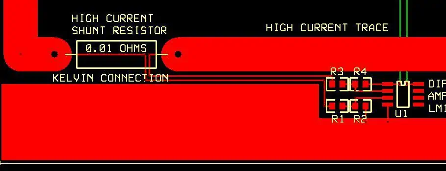
A Kelvin connection refers to a four-wire electrical measurement configuration used to determine the precise resistance of a device under test (DUT) with high accuracy. Kelvin connection printed circuit boards (PCBs) integrate this specialized wiring pattern into the PCB traces to enable accurate on-board resistance measurement of components.
In a Kelvin connection, two wires are used to source current through the DUT while a separate two wires sense the resultant voltage drop. This eliminates errors caused by wiring resistance to achieve micro-ohm precision unmatched by traditional two-wire (non-Kelvin) connections.
High-power PCBs often incorporate current shunts – low value resistors designed to measure current flowing through a circuit. Kelvin connections on the shunt traces allow micro-ohm resolution that improves current measurement accuracy.
Accurate Sensing of Voltage Drops
Minimizing trace resistance allows small voltage drops across PCB nodes to be sensed with less noise using Kelvin connections. This helps calibrate power regulation circuits.
Analyze PCB Copper Integrity
Measuring PCB trace resistances during quality control verifies design integrity and detects defects like cracks or gaps. Kelvin connections provide repeatable precision trace measurements.
Improved Reliability Testing
Monitoring PCB trace resistance changes using Kelvin connections during temperature or vibration testing correlates small damage before outright failure.
Several key guidelines should be followed when laying out Kelvin connections in circuit boards:
1. Minimize Trace Lengths
Keep all 4 traces as short and wide as possible to reduce parasitic resistances.
2. Avoid Trace Bends/Shapes
Refrain from trace angles or shapes which increase impedance through the thin circuit board laminate.
3. Use Copper Fills for Shielding
Adding copper fill shapes connected to ground around the traces shields noise sources.
4. Include Test Points
Test points allow temporary connections to the internal PCB Kelvin wiring to facilitate debugging or failure analysis.
Applications and Usage Examples
Kelvin connection PCB implementations enable precise resistance measurement across a variety of applications:
Power Supply Current Monitoring
Shunt resistors with 4-wire Kelvin connections provide temperature stable, high-resolution current sensing for closed-loop supply regulation.
Battery Pack Wired Resistance Measurement
Cell balancing circuits in battery packs leverage Kelvin connections to measure wiring harness resistances influencing voltage accuracy.
Press Fit Connector Contact Resistance Testing
Measuring contact resistance changes in press-fit PCB connectors during thermal cycling qualifies reliability using mayn dedicated Kelvin connection spring pins.
Continuous PCB Trace Integrity Testing
Running high current loads while continuously monitoring copper trace resistances with Kolvin connections over long time periods assesses reliability.
Biomedical Sensor Calibration
On-board Kelvin wiring allows micro-ohm resolution tuning and calibration of delicate instrumentation amplifier circuits used in medical sensors.
Integrating Kelvin connections into printed circuit board designs enables accurate resistance measurement unachievable by traditional two-wire configurations. By isolating current flow and voltage sense pathways both electrically and physically, noise is reduced achieving micro-ohm precision critical for precision current monitoring, voltage drop sensing, and PCB copper integrity validation. With thoughtful layout and shielding, PCBs with Kelvin connections populate a diversity of applications ranging from power electronics to biomedical instruments.
Frequently Asked Questions
How does a Kelvin connection provide more accurate resistance measurement compared to traditional wiring?
Kelvin connections eliminate the measurement uncertainty caused by parasitic resistance in the wires used to source current by providing a separate isolated pair to sense voltage with ultra low-impedance. This avoids measurement error.
What magnitude of resistances can be measured with Kelvin connected PCBs?
Properly designed Kelvin connections allow resistances from milliohms down to microohms to be resolved. This covers measurement of typical current sense elements, PCB traces, and other integrated resistive components.
Does the thickness and length of the traces impact Kelvin connection performance?
Yes, using shorter and thicker copper traces is critical to minimize trace resistances below the micro-ohm devices under test. Long, thin traces degrade resolution through excessive trace resistance and noise pickup.
How many wires does a Kelvin connection require?
Four wires are needed – two distinct connections to each terminal of the resistive device under test. This provides dedicated current flow and voltage sense pathways to avoid measurement errors.
Can Kelvin connections adjust for temperature drifts during resistance measurement?
Yes, by using temperature calibration standards with known resistance drift specifications and similarly constructing the DUT, temperature induced resistance changes can be accurately measured with the Kelvin connection.
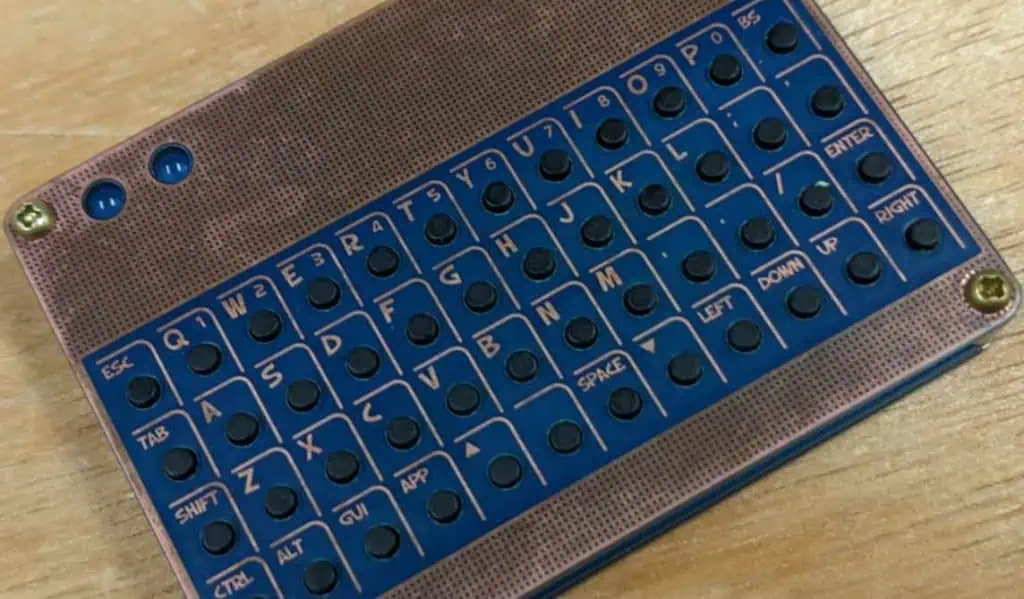
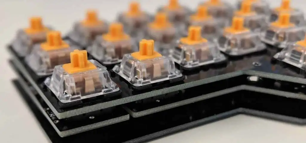
A keyboard PCB tester is a device used to test the functionality and connectivity of a printed circuit board (PCB) designed for a computer keyboard. Keyboard PCB testers allow manufacturers and hobbyists to validate all aspects of a keyboard PCB design before assembling the final keyboard.
Keyboard PCB testers verify the following functions:
Electrical connectivity between switches, microcontrollers, and other PCB components
There are several key benefits to using a keyboard PCB tester during the design and manufacturing process:
Validate PCB Trace Integrity
The PCB tester can validate that all intended electrical connections have been properly etched into the PCB during fabrication. This ensures no broken or partial traces exist on the board that would prevent correct switch matrix scanning.
Reduce Costly Re-spins
By fully testing a keyboard PCB before production, any design flaws can be identified early. This avoids costly PCB re-spins later in the development cycle.
Verify Firmware Compatibility
Testing the PCB with keyboard firmware loaded confirms the microcontroller chip can properly interface with the PCB hardware. Incompatibilities can be addressed in either the PCB or firmware.
Check N-Key Rollover Capability
Keyboard testers enable validating that no ghosting issues occur, even when many keys are pressed simultaneously. This confirms the keyboard matrix can support full NKRO operation.
Streamline Manufacturing Testing
Performing comprehensive tests with a keyboard PCB tester means less testing is needed later during production. This saves manufacturing time and cost.
What to Look for in a Keyboard PCB Tester
There are several key factors to evaluate when selecting a keyboard PCB tester:
Switch Matrix Test Interface
The tester should provide an interface to mount the keyboard PCB and connect switches installed in each position of the switch matrix. This allows scanning of the complete matrix.
Matrix Size
Number of Switches
60%
~60
75%
~80
80%
~85
100% / Full
100-110
Integrated Keycap Simulators
High-quality testers come with physical key actuators to simulate key presses. These can validate the sensor/switch mechanism and provide a realistic typing feel.
MIDI and Audio Output
Test MIDI and audio output generation from the keyboard PCB by connecting to external speakers or a Digital Audio Workstation (DAW).
Firmware Loading Capability
There should be a method to load the keyboard’s firmware onto the microcontroller to test full functionality and compatibility.
NKRO Testing Features
Advanced testers provide specialized interfaces to press multiple switches simultaneously. This confirms the keyboard matrix and firmware supports full NKRO.
Multimeter Probes
Some testers integrate digital multimeter probes to measure continuity, resistance, capacitance, and voltage of PCB components and traces during testing.
Debugging Interfaces
Interfaces like JTAG or SWD allow advanced debugging of the keyboard microcontroller firmware and low-level operation.
Types of Keyboard PCB Test Solutions
There are a variety of keyboard PCB test solutions available depending on application requirements and budget.
Custom Test Fixtures
Fixtures consist of an array of mechanical switches mounted to a baseplate to interface with the keyboard PCB switches and simulate key presses. Custom fixturing provides flexibility to accommodate different PCB sizes but requires fabrication expertise.
Universal Testers
Universal keyboard testers feature an adjustable housing to adapt to different PCB sizes. They integrate keycap simulators, MIDI/Audio validation tools, and debugging features into a single device. These provide excellent functionality but at a high cost.
Popular universal testers include:
GoKey Tester
SO Layer Electronic Keyboard Tester
DIY Testing Stations
Hobbyists often create custom testing devices using DIY electronics kits or prototyping boards like Arduino or Raspberry Pi. These low-cost platforms can interface with keyboard matrices to validate basic functionality but require significant development effort.
The general workflow for testing a keyboard PCB consists of:
1. Mount the PCB
Secure the keyboard PCB into the tester interface with the switch positions properly aligned.
2. Install Firmware
If testing with firmware, load the keyboard firmware hex file onto the microcontroller.
3. Connect Power
Connect the appropriate power source to turn on the keyboard PCB. USB or battery power are typical.
4. Actuate Switches
Manually press buttons on the integrated keycap simulators or external keyboard to actuate each switch position.
5. Validate Matrix Scanning
Monitor the keyboard protocol data using debug software to validate the firmware detects each switch actuation.
6. Test MIDI/Audio Output
If MIDI/Audio features are supported, validate correct waveform generation by connecting speakers or MIDI recording software.
7. Validate NKRO
Using a specialized NKRO interface, press an array of keys simultaneously to confirm no ghosting or blocking occurs.
8. Debug Issues
Use integrated tools like multimeter probes or debugging interfaces to diagnose and fix issues with traces, solder joints, components, or firmware.
Application Examples of Keyboard PCB Test Fixtures
Keyboard PCB testers enable a wide range of applications during design, pre-production, and manufacturing:
Research & Development
Engineers use keyboard test fixtures during R&D to validate PCB designs iteratively without needing complete prototypes.
Design Verification
Quality engineers can formally verify all acceptance criteria are met for connectivity, scanning, rollover, and output generation using detailed test procedures.
Production Line Testing
Streamlined validation procedures with keyboard PCB testers during manufacturing reduce the overhead of quality control processes.
Safety & Compliance
Testing helps certify each keyboard PCB meets electrostatic standards or is compliant with electrical safety regulations for the target market.
Partner/Supplier Qualification
Brands qualifying PCB or electronic component vendors utilize testing to ensure suppliers meet quality benchmarks.
Fault Diagnosis & Repair
Hobbyists and repair technicians leverage DIY keyboard testers to efficiently troubleshoot issues with non-functional keyboards.
Keyboard PCB testers enable validation of all functional aspects of a keyboard PCB design before assembling the final keyboard enclosure and keycaps. By thoroughly testing the bare PCB, manufacturers can identify issues early and reduce costly re-spins later in the process. From simple custom test fixtures to advanced universal solutions, there are tester configurations available for any application need and budget. As keyboards become increasingly complex, keyboard PCB test instrumentation will continue growing as an essential tool for design, pre-production verification, manufacturing, and service workflows.
Frequently Asked Questions
What are the key functions tested by a keyboard PCB tester?
The main functions validated by keyboard PCB testers include: electrical connectivity between PCB components, switch matrix scanning operation, MIDI/audio signal generation, firmware compatibility, and N-key rollover capability.
When in the design flow are keyboard PCB testers used?
Keyboard PCB testers are primarily used to validate designs after fabrication of the bare PCB and before enclosure assembly. This enables issues to be identified early before large production runs occur.
What interface is used to actuate the PCB switches during testing?
Most universal keyboard PCB testers utilize physical actuators to press each switch on the board and simulate key presses. Custom test fixtures generally interface bare switches to mechanically activate the PCB switch sites.
Can hobbyists create their own keyboard testing devices?
Yes, hobbyists can construct custom DIY keyboard test devices using kits based on platforms like Arduino or Raspberry Pi. These low-cost tools allow basic validation but require significant development work.
How are multiple simultaneous key presses tested to validate NKRO ?
Advanced commercial keyboard PCB testers come equipped with specialized interfaces to allow pressing large arrays of keys at once. Signals can then be monitored to check no ghosting or blocking occurs during extreme conditions.