The automotive industry has undergone a dramatic transformation in recent years, with vehicles becoming increasingly reliant on sophisticated electronic systems. From advanced driver assistance systems (ADAS) to infotainment and powertrain control, modern cars are essentially computers on wheels. At the heart of this automotive revolution are car-grade electronics, specifically automotive chips and components designed to withstand the unique challenges of the automotive environment.
This article will explore the world of car-grade electronics, comparing automotive chips and components, and delving into the stringent requirements that set them apart from their consumer-grade counterparts. We’ll examine the key differences, manufacturing processes, and the critical role these specialized electronics play in ensuring the safety, reliability, and performance of modern vehicles.
Understanding Car-Grade Electronics
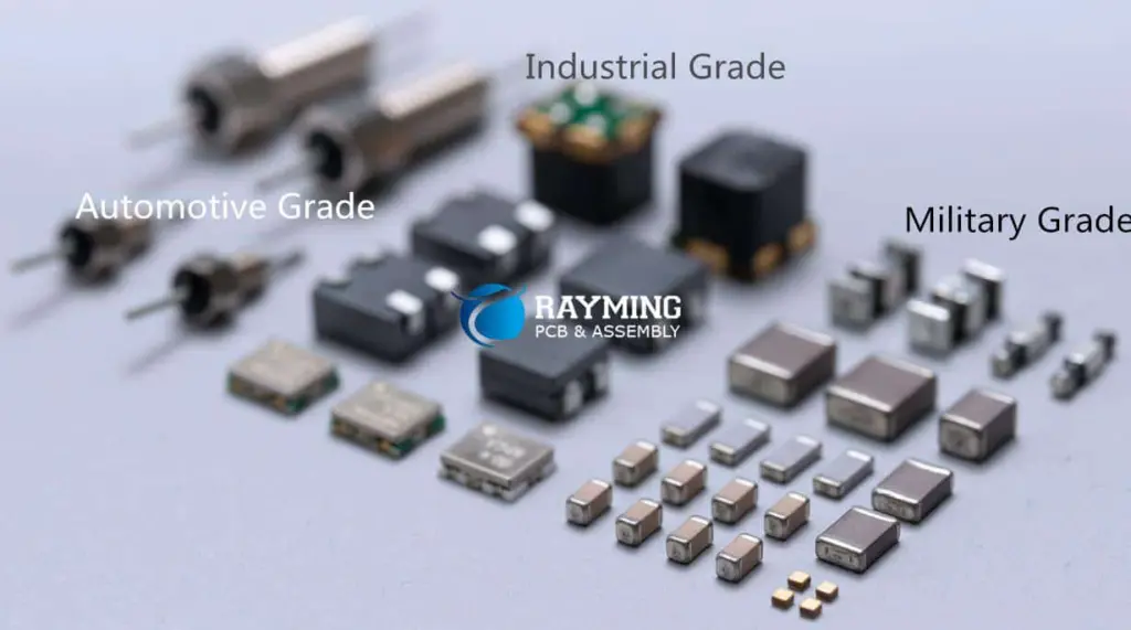
What are car-grade electronics?
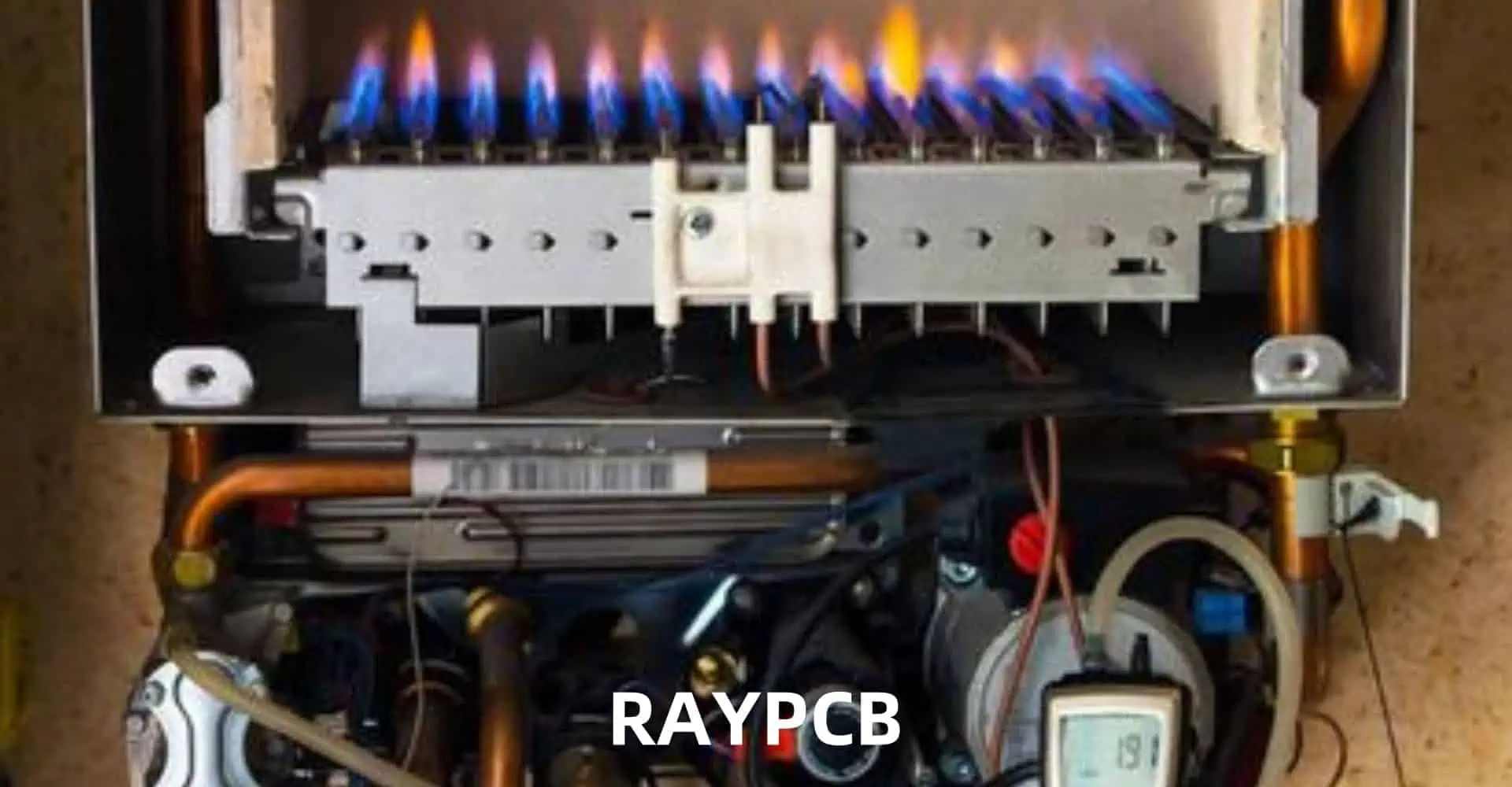
Car-grade electronics, also known as automotive-grade electronics, are electronic components and systems specifically designed and manufactured to meet the rigorous demands of the automotive environment. These electronics must operate reliably under extreme conditions, including:
- Wide temperature ranges
- Vibration and shock
- Electromagnetic interference (EMI)
- Exposure to moisture, chemicals, and contaminants
- Long operational lifetimes
Key differences between automotive and consumer electronics
| Aspect | Automotive Electronics | Consumer Electronics |
| Operating temperature range | -40°C to 125°C or wider | 0°C to 70°C (typical) |
| Expected lifespan | 10-15 years or more | 2-5 years (typical) |
| Reliability requirements | Zero defects, safety-critical | Lower tolerance for failures |
| Environmental conditions | Harsh (vibration, EMI, chemicals) | Controlled environments |
| Development cycle | 3-5 years | 6-18 months |
| Cost | Higher due to specialized manufacturing | Lower, mass-produced |
| Regulatory compliance | Strict automotive standards (e.g., ISO 26262) | Less stringent consumer st |
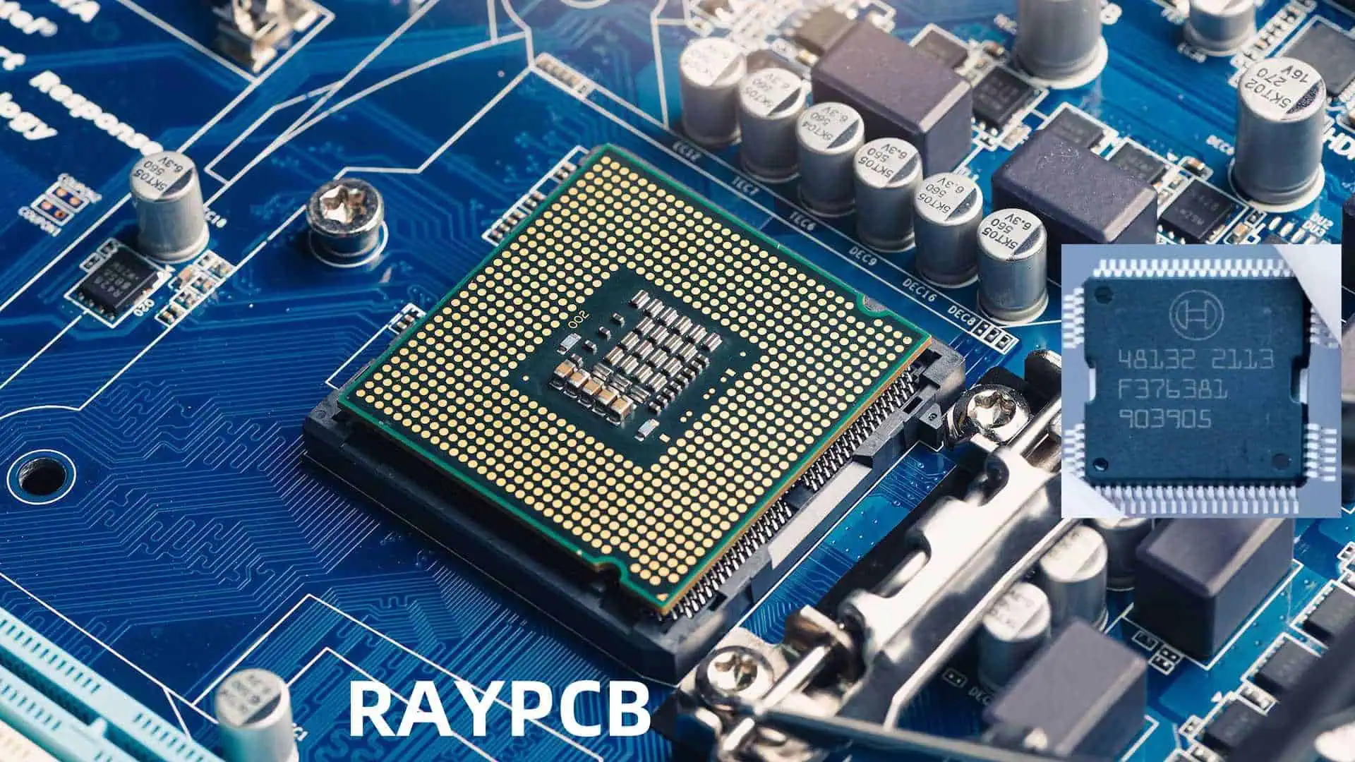
Automotive Chips: The Brain of Modern Vehicles
Types of automotive chips
Automotive chips can be categorized into several types based on their functions:
- Microcontrollers (MCUs)
- Microprocessors (MPUs)
- Field-Programmable Gate Arrays (FPGAs)
- Application-Specific Integrated Circuits (ASICs)
- Power Management Integrated Circuits (PMICs)
- Sensor Chips
Key features of automotive chips
Temperature resistance
Automotive chips must function reliably across a wide temperature range, typically from -40°C to 125°C or even wider. This requirement stems from the varied environments vehicles operate in, from arctic cold to desert heat.
Durability and longevity
Car-grade chips are designed for extended operational lifetimes, often 10-15 years or more. This longevity is crucial for ensuring vehicle reliability and reducing maintenance costs over the vehicle’s lifespan.
Electromagnetic compatibility (EMC)
Automotive chips must be designed to resist electromagnetic interference (EMI) and not emit excessive electromagnetic radiation that could interfere with other vehicle systems or nearby electronics.
Fault tolerance and redundancy
Safety-critical automotive chips often incorporate fault-tolerant designs and redundancy to ensure continued operation even in the event of partial failures.
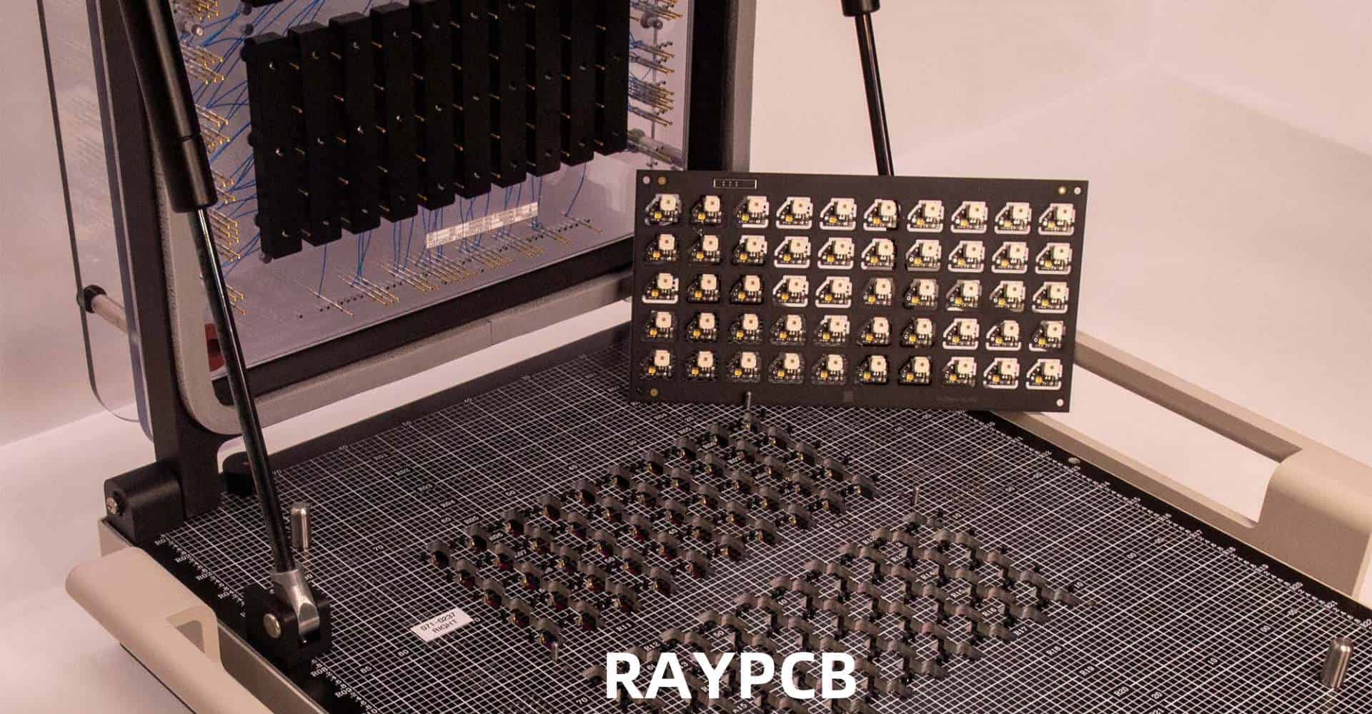
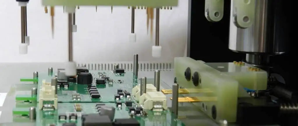
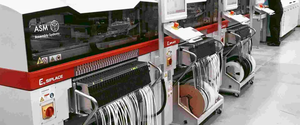
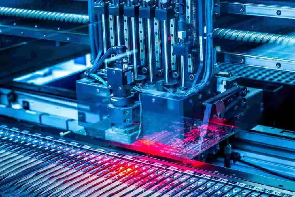
Manufacturing processes for automotive chips
Automotive chip manufacturing involves several specialized processes to ensure reliability and durability:
- Wafer-level chip-scale packaging (WLCSP)
- Flip-chip ball grid array (FCBGA)
- Enhanced quality control and testing
- Specialized materials for improved thermal management
Automotive chip standards and certifications
Automotive chips must comply with various industry standards and certifications, including:
- AEC-Q100 (for integrated circuits)
- ISO 26262 (functional safety for road vehicles)
- ASIL (Automotive Safety Integrity Level) classifications
- IATF 16949 (quality management system)
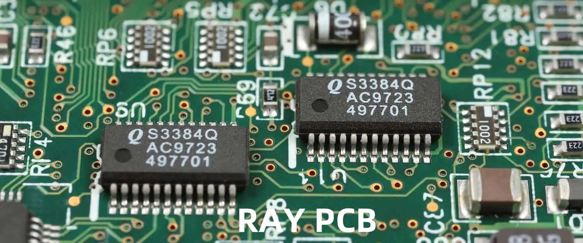
Automotive Components: Building Blocks of Vehicle Electronics
Types of automotive components
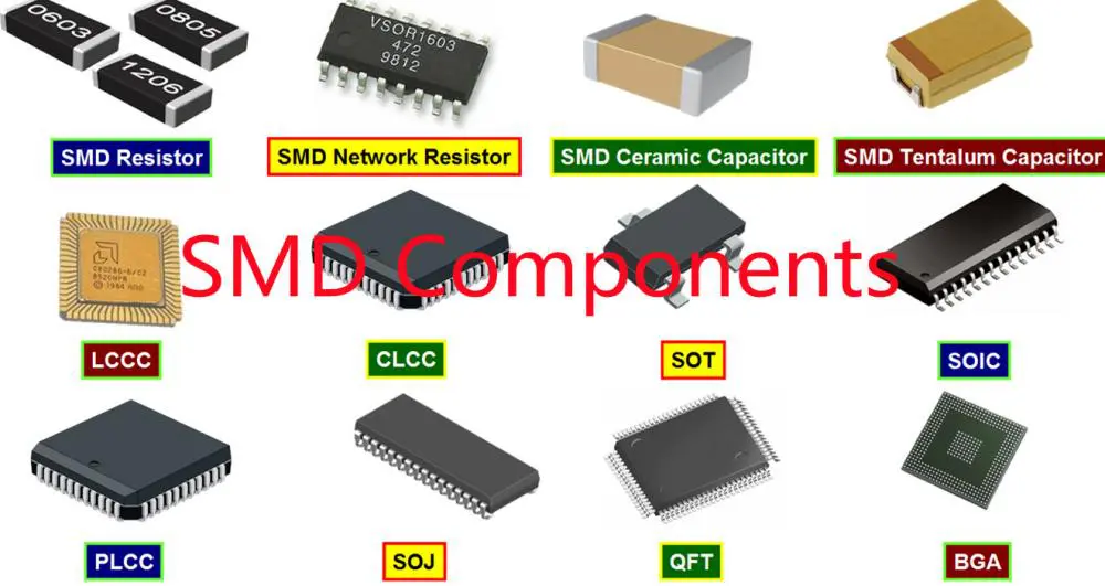
Automotive components encompass a wide range of electronic parts, including:
- Resistors
- Capacitors
- Inductors
- Diodes
- Transistors
- Connectors
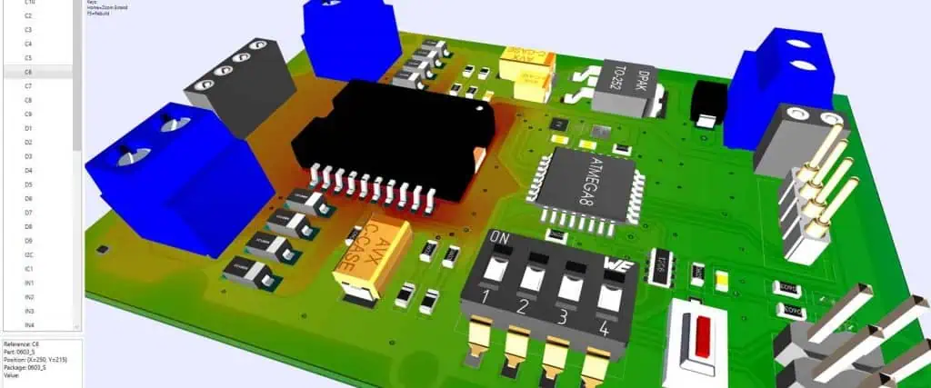
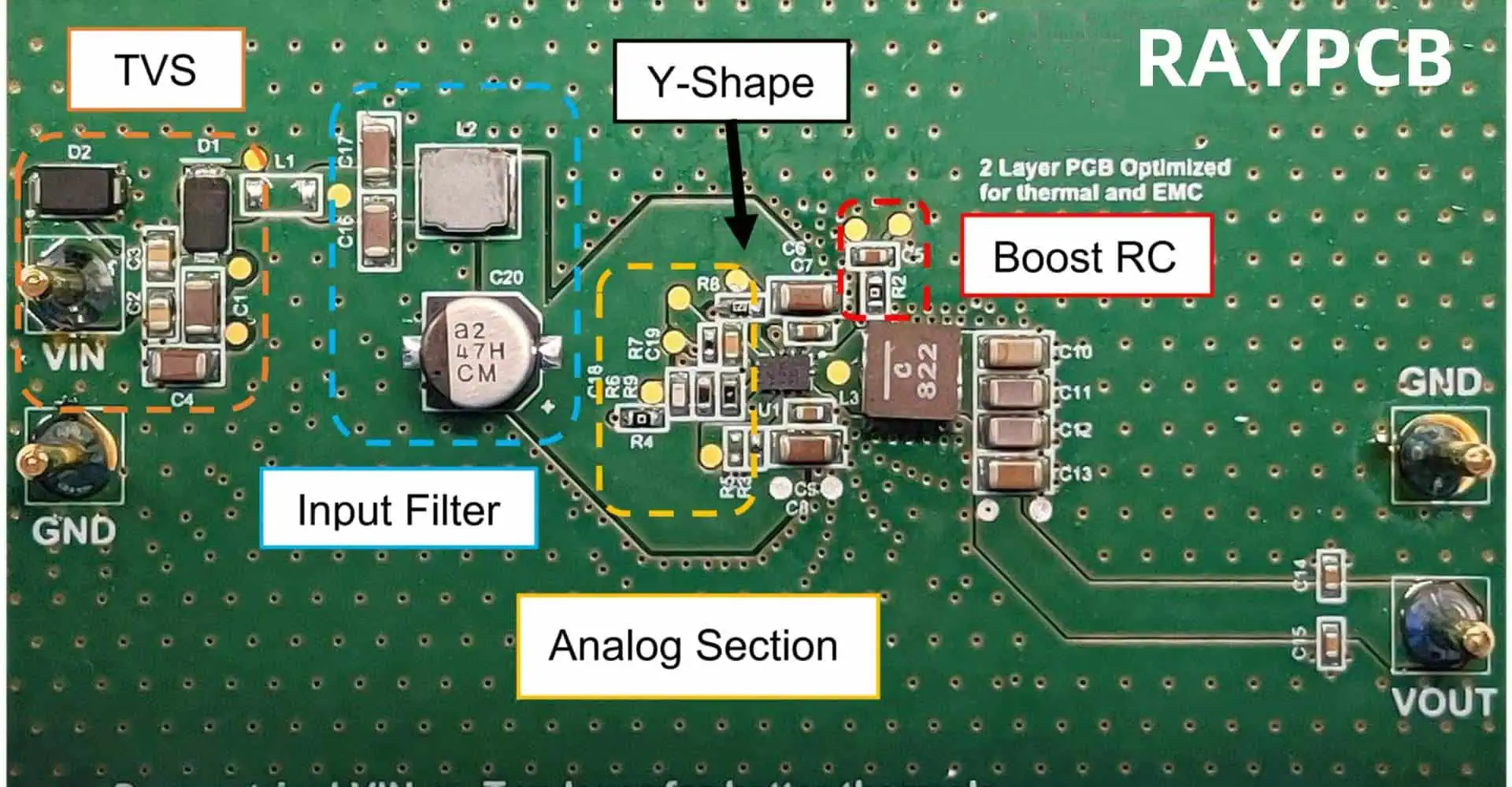
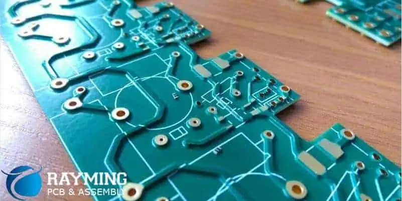
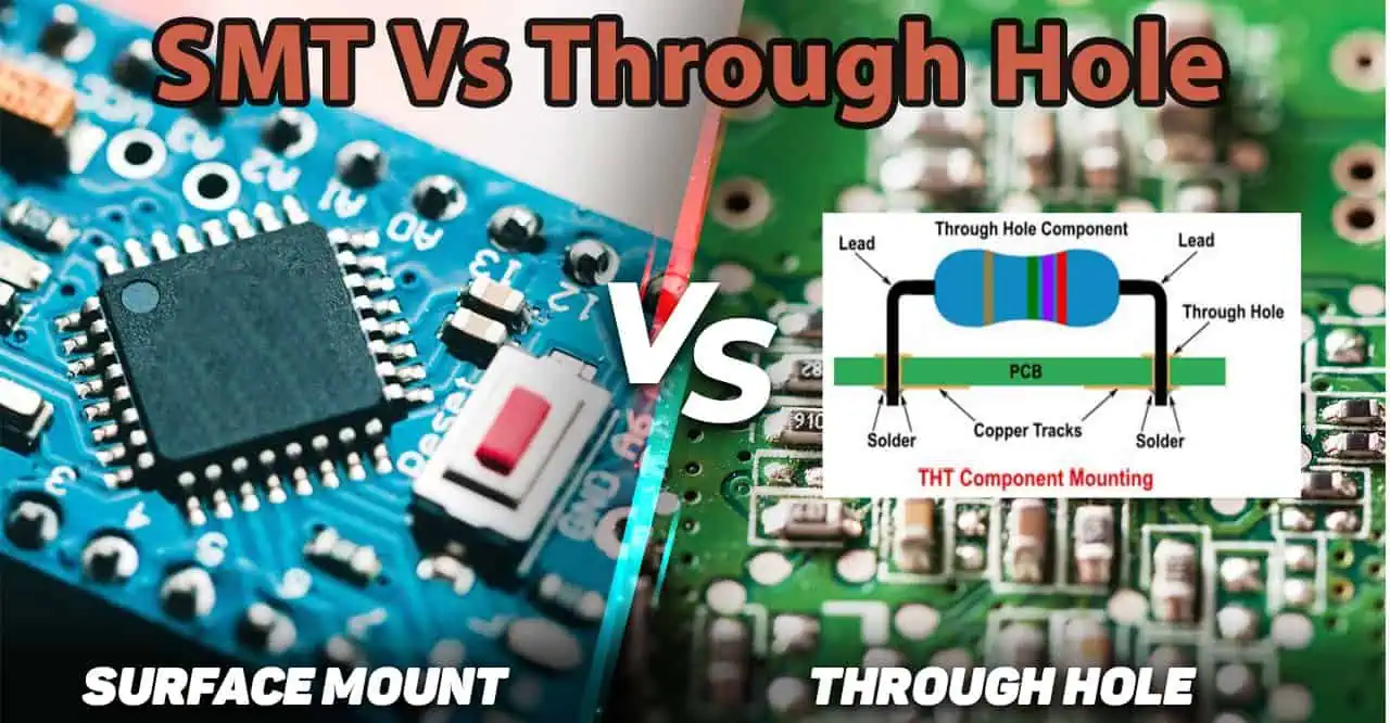
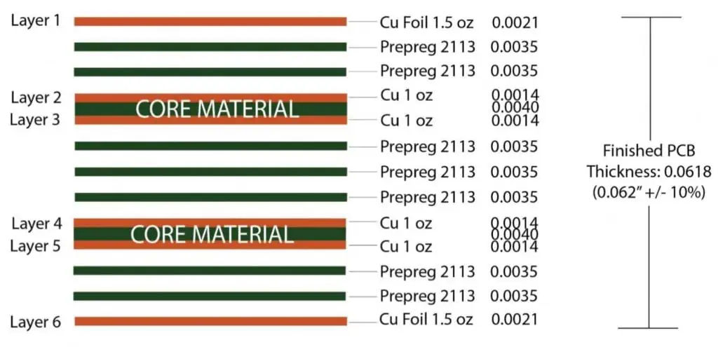
- Printed Circuit Boards (PCBs)
- Sensors and actuators
Key features of automotive components
Vibration and shock resistance
Automotive components must withstand constant vibration and occasional shocks without failure. This is achieved through specialized design and materials selection.
Corrosion resistance
Components used in automotive applications are often exposed to harsh environments, including moisture, salt, and various chemicals. Corrosion-resistant materials and protective coatings are essential for longevity.
Thermal cycling endurance

Automotive components must withstand repeated thermal cycling without degradation or failure. This is particularly important for components in engine compartments or other areas subject to significant temperature fluctuations.
High-reliability connectors
Automotive connectors must maintain reliable electrical connections despite vibration, thermal cycling, and exposure to contaminants.
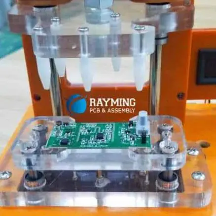
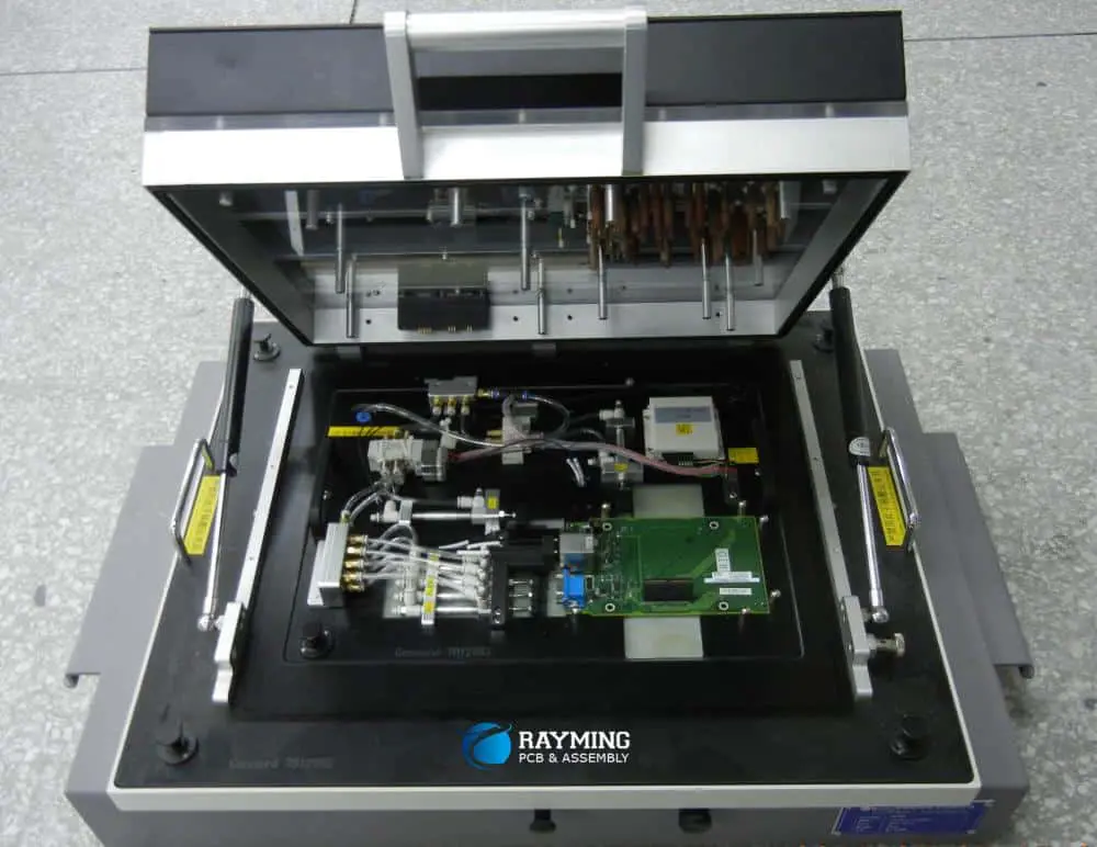
Manufacturing processes for automotive components
Automotive component manufacturing involves specialized processes to ensure reliability:
- Automated optical inspection (AOI)
- X-ray inspection for internal defects
- Environmental stress screening (ESS)
- Burn-in testing for early failure detection
Automotive component standards and certifications
Automotive components must meet various standards, including:
- AEC-Q200 (for passive components)
- AEC-Q101 (for discrete semiconductors)
- USCAR specifications for connectors
- IPC standards for PCB manufacturing
Comparing Automotive Chips and Components
Functionality and complexity
| Aspect | Automotive Chips | Automotive Components |
| Complexity | High (integrated circuits) | Low to moderate (discrete parts) |
| Functionality | Processing, control, memory | Basic electrical functions |
| Customization | Often application-specific | More standardized |
| Integration level | High (multiple functions) | Low (single function) |
Manufacturing challenges
| Challenge | Automotive Chips | Automotive Components |
| Process control | Extremely tight tolerances | Moderate to tight tolerances |
| Cleanliness requirements | Ultra-clean room conditions | Clean room conditions |
| Defect rates | Near-zero defect rates required | Very low defect rates required |
| Testing complexity | Extensive functional and parametric testing | Typically simpler electrical testing |
Cost considerations
| Factor | Automotive Chips | Automotive Components |
| Development costs | Very high (design and validation) | Moderate (adaptation of existing designs) |
| Production volume | Medium to high | High to very high |
| Unit cost | Higher due to complexity | Lower, but varies widely |
| Testing costs | Significant (functional and reliability) | Moderate (mostly parametric) |
Supply chain considerations
| Aspect | Automotive Chips | Automotive Components |
| Lead times | Longer (complex manufacturing) | Shorter (simpler production) |
| Supplier diversity | Limited (specialized manufacturers) | Broader range of suppliers |
| Inventory management | Critical (long lead times) | Important but more flexible |
| Obsolescence risk | Higher (rapid technology changes) | Lower (more standardized parts) |
The Role of Car-Grade Electronics in Vehicle Systems
Powertrain control
Automotive chips and components play a crucial role in managing the vehicle’s powertrain, including:
- Engine control units (ECUs)
- Transmission control modules
- Battery management systems for electric vehicles
- Fuel injection and ignition control
Safety systems
Car-grade electronics are essential for various safety systems:
- Antilock braking systems (ABS)
- Electronic stability control (ESC)
- Airbag deployment systems
- Tire pressure monitoring systems (TPMS)
Advanced Driver Assistance Systems (ADAS)
ADAS rely heavily on sophisticated automotive chips and sensors:
- Radar and LiDAR systems
- Camera-based vision systems
- Adaptive cruise control
- Lane departure warning and lane keeping assist
Infotainment and connectivity
Modern vehicle infotainment systems incorporate various car-grade electronics:
- Head units with powerful processors
- Audio amplifiers and digital signal processors
- Connectivity modules (Bluetooth, Wi-Fi, cellular)
- Display drivers and touch controllers
Challenges and Future Trends in Car-Grade Electronics

Increasing complexity and integration
As vehicles become more advanced, the complexity of automotive electronics continues to grow. This trend presents several challenges:
- System-on-Chip (SoC) integration for reduced space and power consumption
- Managing thermal issues in highly integrated systems
- Ensuring reliability with increasing transistor densities
- Balancing performance requirements with power efficiency
Electrification and autonomous driving
The shift towards electric vehicles and autonomous driving capabilities is driving significant changes in car-grade electronics:
- High-voltage and high-current components for electric powertrains
- Advanced sensor fusion and processing for autonomous systems
- Redundancy and fail-safe designs for safety-critical functions
- Real-time processing capabilities for decision-making in autonomous vehicles
Cybersecurity concerns
As vehicles become more connected, cybersecurity becomes increasingly important:
- Secure boot and firmware update mechanisms
- Hardware-based security features (e.g., trusted platform modules)
- Encryption and authentication for in-vehicle networks
- Intrusion detection and prevention systems
Sustainability and environmental concerns
The automotive industry is under pressure to improve sustainability, affecting car-grade electronics:
- Design for recyclability and easy disassembly
- Reduction of hazardous materials in electronic components
- Improved energy efficiency to extend electric vehicle range
- Longer-lasting electronics to reduce electronic waste
Conclusion
Car-grade electronics, encompassing both automotive chips and components, form the backbone of modern vehicle systems. These specialized electronic parts must meet stringent requirements for reliability, durability, and performance in the harsh automotive environment. As vehicles continue to evolve, becoming more electrified, connected, and autonomous, the role of car-grade electronics will only grow in importance.
The distinction between automotive chips and components lies primarily in their complexity and functionality, with chips providing the “brains” of vehicle systems and components serving as the essential building blocks. Both categories require specialized manufacturing processes, rigorous testing, and compliance with automotive industry standards to ensure they can withstand the challenges of automotive use.
As the automotive industry continues to evolve, car-grade electronics will play a pivotal role in shaping the future of transportation. From improving safety and efficiency to enabling new features and capabilities, these specialized electronic parts will continue to drive innovation in the automotive sector.
FAQ
- Q: What is the main difference between automotive-grade and consumer-grade electronics? A: The main differences lie in their durability, reliability, and operating conditions. Automotive-grade electronics are designed to function in harsh environments with extreme temperatures (-40°C to 125°C or wider), vibration, and electromagnetic interference. They also have longer expected lifespans (10-15 years or more) and must meet stricter quality and safety standards. Consumer-grade electronics typically operate in more controlled environments, have shorter lifespans, and are subject to less stringent requirements.
- Q: Why are automotive chips more expensive than consumer chips? A: Automotive chips are more expensive due to several factors:
- Rigorous design and testing processes to ensure reliability and safety
- Specialized manufacturing techniques and materials for extreme conditions
- Lower production volumes compared to consumer electronics
- Compliance with strict automotive industry standards and certifications
- Extended support and availability requirements (often 10-15 years or more) These factors contribute to higher development and production costs, which are reflected in the final price of automotive chips.
- Q: What is the AEC-Q100 standard, and why is it important for automotive chips? A: AEC-Q100 is a failure mechanism based stress test qualification for integrated circuits, established by the Automotive Electronics Council (AEC). It is important because it sets the minimum stress test qualifications for automotive-grade integrated circuits. The standard ensures that chips can withstand the harsh automotive environment and meet the industry’s reliability requirements. Compliance with AEC-Q100 is often a prerequisite for chips to be used in automotive applications, as it demonstrates their ability to function reliably under extreme conditions.
- Q: How do automotive components differ from automotive chips in terms of manufacturing and testing? A: While both automotive components and chips undergo rigorous manufacturing and testing processes, there are some key differences:
- Complexity: Chip manufacturing involves more complex processes and tighter tolerances.
- Testing: Chips require more extensive functional and parametric testing, while components often undergo simpler electrical testing.
- Production volume: Components are typically produced in higher volumes than specialized automotive chips.
- Customization: Chips are often more customized for specific applications, while components tend to be more standardized. Both categories must meet strict quality standards, but the specific requirements and processes can vary based on the type of part and its intended use in the vehicle.
- Q: What are the main challenges facing the automotive electronics industry in the coming years? A: The main challenges include:
- Increasing complexity and integration of electronic systems
- Meeting the demands of electrification and autonomous driving technologies
- Ensuring cybersecurity in increasingly connected vehicles
- Addressing sustainability and environmental concerns
- Managing supply chain issues and potential component shortages
- Keeping pace with rapid technological advancements while maintaining long-term support
- Balancing cost pressures with the need for high-reliability, automotive-grade components These challenges will require ongoing innovation in design, manufacturing, and testing of car-grade electronics to meet the evolving needs of the automotive industry.