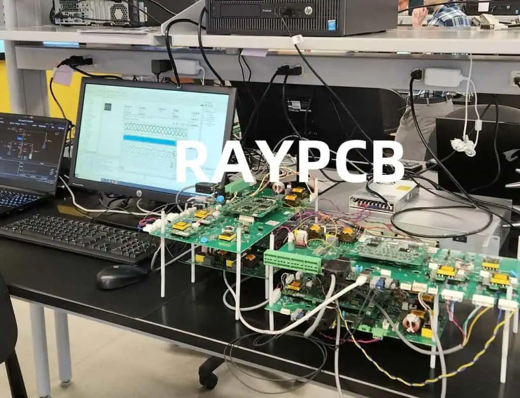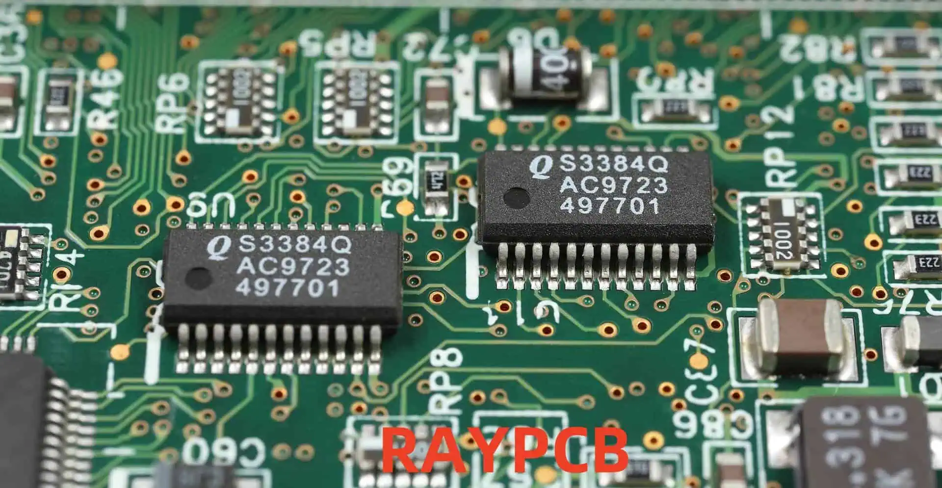
Printed Circuit Boards (PCBs) are the unsung heroes of modern electronics. These intricate networks of conductors and components form the backbone of nearly every electronic device we use today. While most people are familiar with the green boards found inside computers and smartphones, there’s much more to PCBs than meets the eye. In this article, we’ll explore six fascinating facts about PCBs that might surprise even the most tech-savvy individuals.
1. PCBs Have a Rich History Dating Back to World War II
The Birth of Modern Electronics
The story of PCBs begins in the early 20th century, but it was during World War II that they truly came into their own. The need for reliable and compact electronic systems in military equipment drove rapid innovation in circuit board technology.
From Point-to-Point to Printed Circuits
Before PCBs, electronic components were connected using point-to-point construction. This method was time-consuming, prone to errors, and resulted in bulky, unreliable devices. The development of PCBs revolutionized electronics manufacturing by providing a more efficient and reliable alternative.
Key Milestones in PCB History
| Color | Common Uses | Characteristics |
| Green | General electronics | Traditional, most common |
| Blue | Aerospace, medical devices | High contrast for inspection |
| Red | Telecommunications | Heat resistant |
| Black | Audio equipment | Reduces light reflection |
| White | LED applications | Enhances light reflection |
| Yellow | Automotive | High visibility for safety |
| Purple | Military and defense | Specific military standards |
The evolution of PCBs from wartime necessity to commercial ubiquity is a testament to their versatility and importance in modern electronics.
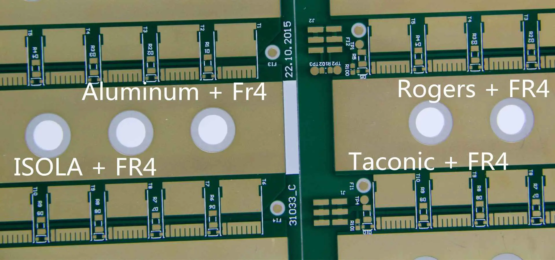
2. PCBs Come in a Rainbow of Colors
Beyond the Traditional Green
When most people think of PCBs, they picture the iconic green boards found in many electronic devices. However, PCBs actually come in a wide variety of colors, each serving a specific purpose or adhering to certain industry standards.
The Colorful World of PCBs
| Characteristic | Rigid PCBs | Flexible PCBs | Stretchable PCBs |
| Base Material | FR-4, ceramic | Polyimide, polyester | Elastomers, silicone |
| Flexibility | None | Can bend and fold | Can elongate |
| Durability | High | Medium to High | Medium |
| Cost | Lower | Higher | Highest |
| Space Efficiency | Low | High | Very High |
| Weight | Heavier | Lighter | Lightest |
| Application Range | Wide | Specialized | Highly specialized |
The Significance of PCB Colors
While the color of a PCB doesn’t directly affect its electrical performance, it can serve several important functions:
- Identification: Different colors can help manufacturers quickly identify board types or revisions.
- Inspection: Some colors provide better contrast, making visual inspection easier.
- Thermal Management: Certain colors can help with heat dissipation or retention.
- Aesthetics: In consumer electronics, PCB color can be chosen to match product design.
- Industry Standards: Some industries have color preferences or requirements for PCBs.
Understanding the diverse palette of PCB colors reveals the thoughtful design considerations that go into even the most minute aspects of electronic manufacturing.
3. PCBs Can Be Flexible and Even Stretchable
Breaking the Rigid Mold
While traditional PCBs are rigid, technological advancements have led to the development of flexible and even stretchable PCBs. These innovations are opening up new possibilities in electronics design and application.
Flexible PCBs
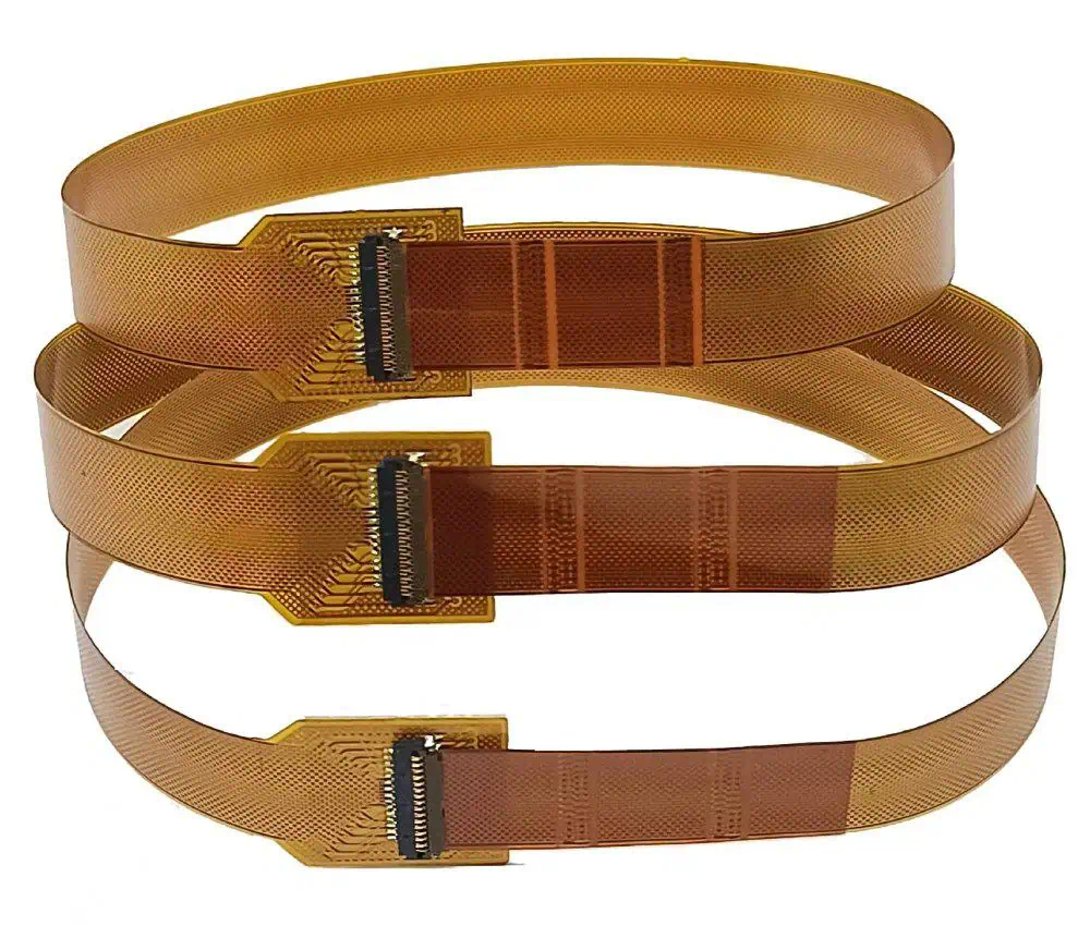
Flexible PCBs (or flex PCBs) are made using flexible base materials like polyimide or polyester films. They can bend, fold, and conform to various shapes, making them ideal for applications where space is at a premium or where the PCB needs to fit into unconventional spaces.
Applications of Flexible PCBs
- Smartphones and tablets
- Wearable technology
- Medical devices (e.g., pacemakers)
- Automotive electronics
- Aerospace systems
Stretchable PCBs
Taking flexibility even further, stretchable PCBs can elongate and return to their original shape without losing functionality. This emerging technology is still in its early stages but shows great promise for future applications.
Potential Uses for Stretchable PCBs
- Smart clothing
- Biomedical implants
- Soft robotics
- Human-machine interfaces
- Structural health monitoring
Comparison: Rigid vs. Flexible vs. Stretchable PCBs
| Era | Typical Maximum Layers | Common Applications |
| 1960s | 4 layers | Early computers |
| 1980s | 8-12 layers | Personal computers |
| 2000s | 20-30 layers | Servers, high-end electronics |
| 2020s | 50+ layers | Supercomputers, advanced telecommunications |
The development of flexible and stretchable PCBs demonstrates the ongoing innovation in the field of electronics, pushing the boundaries of what’s possible in device design and functionality.
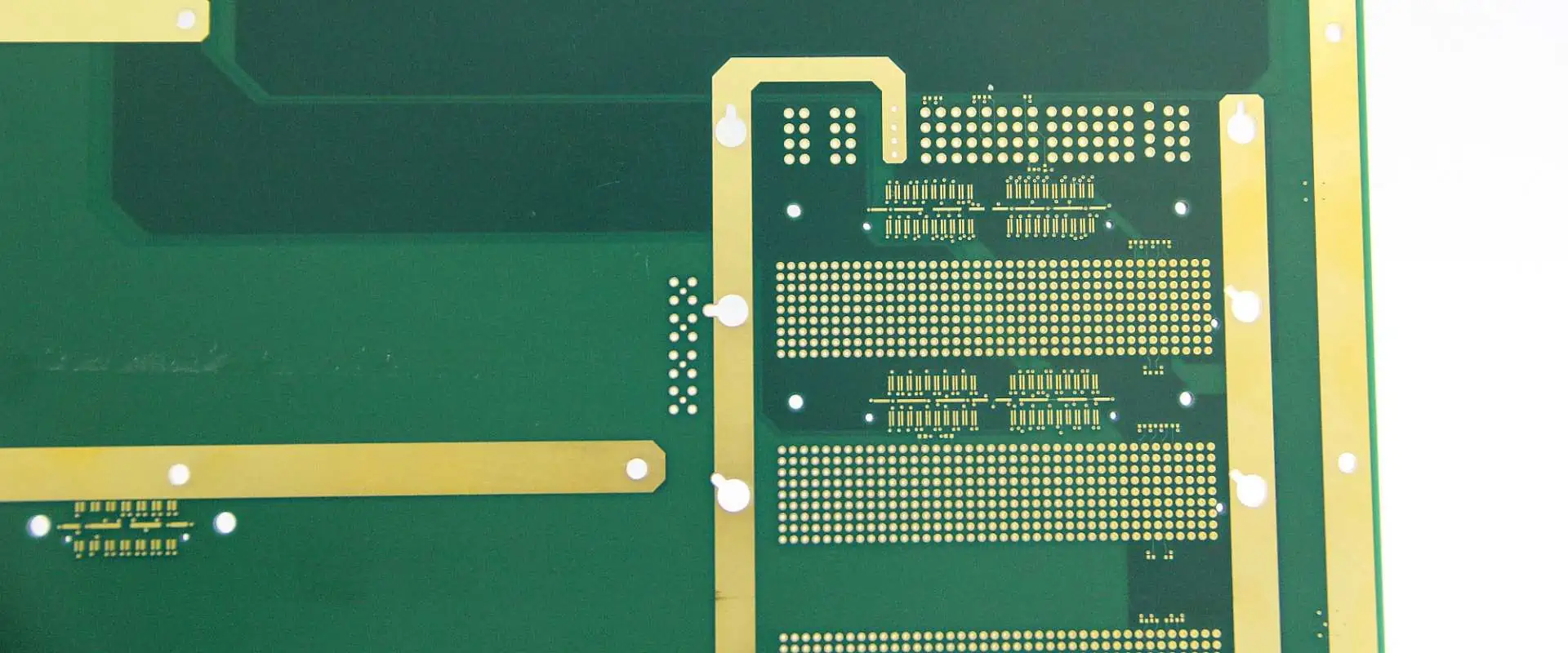
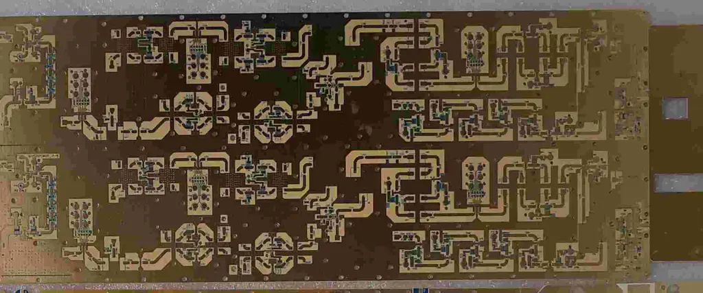
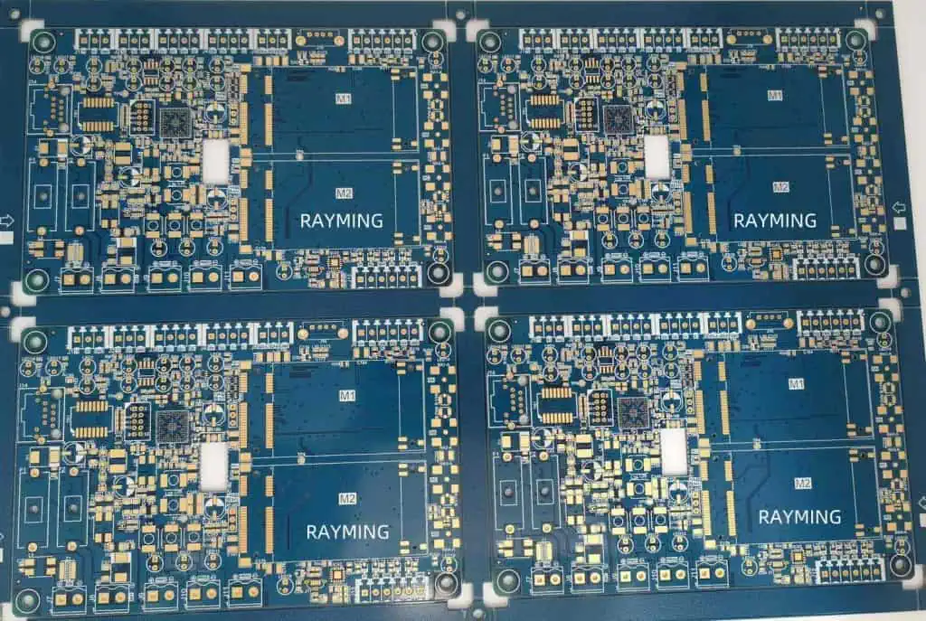
4. PCBs Can Have Up to 50+ Layers
The World of Multilayer PCBs
While simple electronic devices might use single or double-layer PCBs, complex systems often require multilayer boards. These PCBs consist of multiple layers of conductive material separated by insulating layers, allowing for incredibly dense and complex circuitry.
The Evolution of PCB Layers
| Era | Typical Maximum Layers | Common Applications |
| 1960s | 4 layers | Early computers |
| 1980s | 8-12 layers | Personal computers |
| 2000s | 20-30 layers | Servers, high-end electronics |
| 2020s | 50+ layers | Supercomputers, advanced telecommunications |
Benefits of Multilayer PCBs
- Increased Circuit Density: More layers allow for more components and connections in a smaller area.
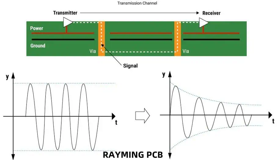
- Improved Signal Integrity: Dedicated ground and power planes reduce noise and interference.
- Better EMI Shielding: Multiple layers can provide better protection against electromagnetic interference.
- Enhanced Thermal Management: More layers can help distribute and dissipate heat more effectively.
- Reduced Size and Weight: Complex circuits can be packed into smaller, lighter boards.
Challenges of High Layer Count PCBs
While the benefits of multilayer PCBs are significant, they also present unique challenges:
- Manufacturing Complexity: Each additional layer increases the difficulty and cost of production.
- Signal Propagation: Signals traveling through many layers can experience delays and distortion.
- Thermal Management: Heat dissipation becomes more complex with tightly packed layers.
- Testing and Troubleshooting: Identifying issues in deeply buried layers can be challenging.
Despite these challenges, the demand for ever-more complex and compact electronic devices continues to drive innovation in multilayer PCB technology.
5. PCBs Can Be Manufactured with Embedded Components
Revolutionizing PCB Design
Embedded component technology is a cutting-edge approach to PCB manufacturing where components are integrated directly into the inner layers of the board. This technique represents a significant leap forward in electronics miniaturization and performance optimization.
Types of Embedded Components
- Active Components: Transistors, ICs, LEDs
- Passive Components: Resistors, capacitors, inductors
Advantages of Embedded Component Technology
| Advantage | Description |
| Size Reduction | Components embedded within layers save surface space |
| Improved Performance | Shorter connection paths reduce signal delays and interference |
| Enhanced Reliability | Protected components are less susceptible to environmental factors |
| Better Thermal Management | Improved heat distribution throughout the board |
| Increased Design Flexibility | Allows for more creative and efficient circuit layouts |
Challenges and Considerations
While embedded component technology offers numerous benefits, it also presents some challenges:
- Manufacturing Complexity: Requires specialized equipment and processes
- Cost: Initially more expensive than traditional PCB manufacturing
- Repairability: Embedded components are difficult or impossible to replace
- Testing: Requires advanced techniques to ensure proper functionality
Despite these challenges, embedded component technology is gaining traction in industries where size, performance, and reliability are critical, such as aerospace, medical devices, and high-end consumer electronics.
6. PCBs Can Be Manufactured Using 3D Printing Technology
The Future of PCB Prototyping and Production
3D printing, also known as additive manufacturing, is revolutionizing many industries, and PCB manufacturing is no exception. While traditional PCB manufacturing methods remain dominant for large-scale production, 3D printing offers exciting possibilities for rapid prototyping and small-batch production.
3D Printed PCB Manufacturing Methods
- Fused Deposition Modeling (FDM): Layering conductive and non-conductive materials
- Stereolithography (SLA): Using photosensitive resins and conductive inks
- Aerosol Jet Printing: Depositing nano-particle inks for fine-pitch circuits
Comparison: Traditional vs. 3D Printed PCBs
| Aspect | Traditional PCBs | 3D Printed PCBs |
| Production Speed | Slower for prototypes | Rapid prototyping |
| Minimum Feature Size | Very small (0.1mm or less) | Larger (0.5mm typical) |
| Material Options | Limited | Diverse, including flexible materials |
| Cost for Small Batches | Higher | Lower |
| Environmental Impact | Higher (chemical processes) | Lower (less waste) |
| Complexity | High | Medium to High |
| Scalability | Excellent | Limited |
Applications and Future Prospects
3D printed PCBs are particularly useful in:
- Rapid prototyping for product development
- Custom electronics for research and education
- Small-batch production for specialized devices
- Creating unique form factors and flexible circuits
As 3D printing technology continues to advance, we can expect improvements in resolution, material properties, and production speed. This could lead to more widespread adoption of 3D printed PCBs in various industries, potentially revolutionizing the way we design and manufacture electronic devices.
Frequently Asked Questions (FAQ)
1. What does PCB stand for, and what is its primary function?
PCB stands for Printed Circuit Board. Its primary function is to mechanically support and electrically connect electronic components using conductive tracks, pads, and other features etched from copper sheets laminated onto a non-conductive substrate.
2. How long does it typically take to manufacture a PCB?
The time to manufacture a PCB can vary widely depending on complexity, number of layers, and production volume. For simple boards, it can take as little as 24 hours for prototypes. More complex multilayer boards or large production runs can take several weeks.
3. Are PCBs recyclable?
Yes, PCBs are recyclable, but the process is complex due to the variety of materials used in their construction. Specialized e-waste recycling facilities can extract valuable metals like copper and gold from PCBs while safely disposing of potentially harmful substances.
4. What’s the difference between a PCB and a PCBA?
A PCB (Printed Circuit Board) is the bare board with conductive tracks but no components. A PCBA (Printed Circuit Board Assembly) is a PCB that has had components soldered onto it, creating a functional electronic circuit.
5. Can PCBs be repaired if damaged?
In many cases, PCBs can be repaired if damaged. Common repairs include replacing damaged components, repairing broken traces, and fixing solder joints. However, the feasibility and cost-effectiveness of repair depend on the extent of the damage and the complexity of the board.
In conclusion, PCBs are fascinating pieces of technology that continue to evolve and shape the world of electronics. From their colorful appearances to their flexible forms and embedded components, PCBs are far more diverse and complex than many people realize. As technology advances, we can expect to see even more innovations in PCB design and manufacturing, further pushing the boundaries of what’s possible in electronic devices.