In the ever-evolving landscape of electronics manufacturing, Printed Circuit Board (PCB) testing and measurement techniques play a crucial role in ensuring product quality, reliability, and performance. As PCBs become more complex, with higher component densities, faster signal speeds, and stricter performance requirements, the methods used to test and measure them must also advance. This article explores the latest developments in PCB test and measurement techniques, highlighting innovative approaches that are shaping the future of electronics quality assurance.
The Evolving Landscape of PCB Complexity
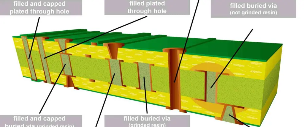
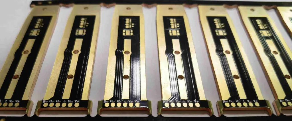
Miniaturization and Increased Density
Modern PCBs are characterized by:
- Smaller component sizes (e.g., 0201, 01005 packages)
- Higher component density
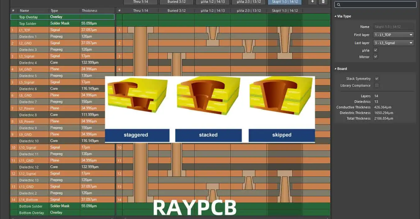
- Multi-layer designs (sometimes exceeding 20 layers)
- Micro vias and buried vias
These factors create new challenges for traditional test and measurement methods.
Higher Frequencies and Faster Edge Rates
With the advent of 5G, IoT, and high-speed computing:
- Signal frequencies now routinely exceed 5 GHz
- Edge rates have decreased to picoseconds
- Signal integrity has become a critical concern
Advanced Materials and Manufacturing Processes
New PCB materials and manufacturing techniques include:
- High-frequency laminates (e.g., PTFE, ceramic-filled hydrocarbon)
- Flexible and rigid-flex PCBs
- 3D-printed electronics
These advancements require adapted test and measurement approaches.
Emerging Test and Measurement Techniques
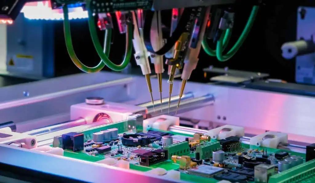
Advanced Optical Inspection
3D Automated Optical Inspection (AOI)
3D AOI systems use multiple cameras and advanced algorithms to create a three-dimensional image of the PCB, allowing for:
- Detection of coplanarity issues
- Measurement of solder paste volume
- Inspection of component placement in three dimensions
AI-Enhanced Defect Detection
Machine learning algorithms are being integrated into optical inspection systems to:
- Improve defect detection accuracy
- Reduce false positives
- Adapt to new defect types without reprogramming
X-ray Inspection Advancements
High-Resolution Digital Tomosynthesis
This technique creates detailed 3D images of PCB layers, enabling:
- Inspection of hidden solder joints (e.g., BGAs, QFNs)
- Detection of voids in solder joints
- Analysis of internal PCB structures
AI-Assisted X-ray Analysis
Machine learning algorithms help in:
- Automating void calculation
- Detecting subtle defects in complex assemblies
- Reducing operator dependency in interpretation
Advanced Electrical Testing
Boundary Scan and JTAG Enhancements
New developments in boundary scan technology include:
- Increased test coverage for high-speed interfaces
- Integration with functional testing
- Improved diagnostics for complex SoC devices
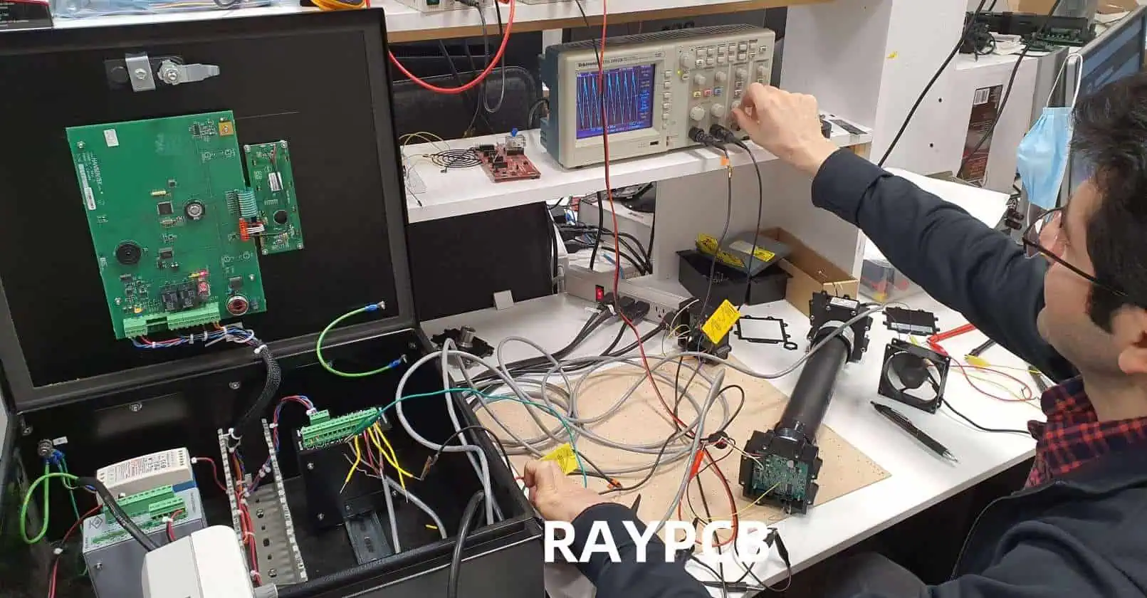
Flying Probe with Thermal Imaging
Combining flying probe testing with thermal imaging allows for:
- Detection of thermal anomalies during electrical testing
- Identification of power-related issues
- Correlation of electrical and thermal performance
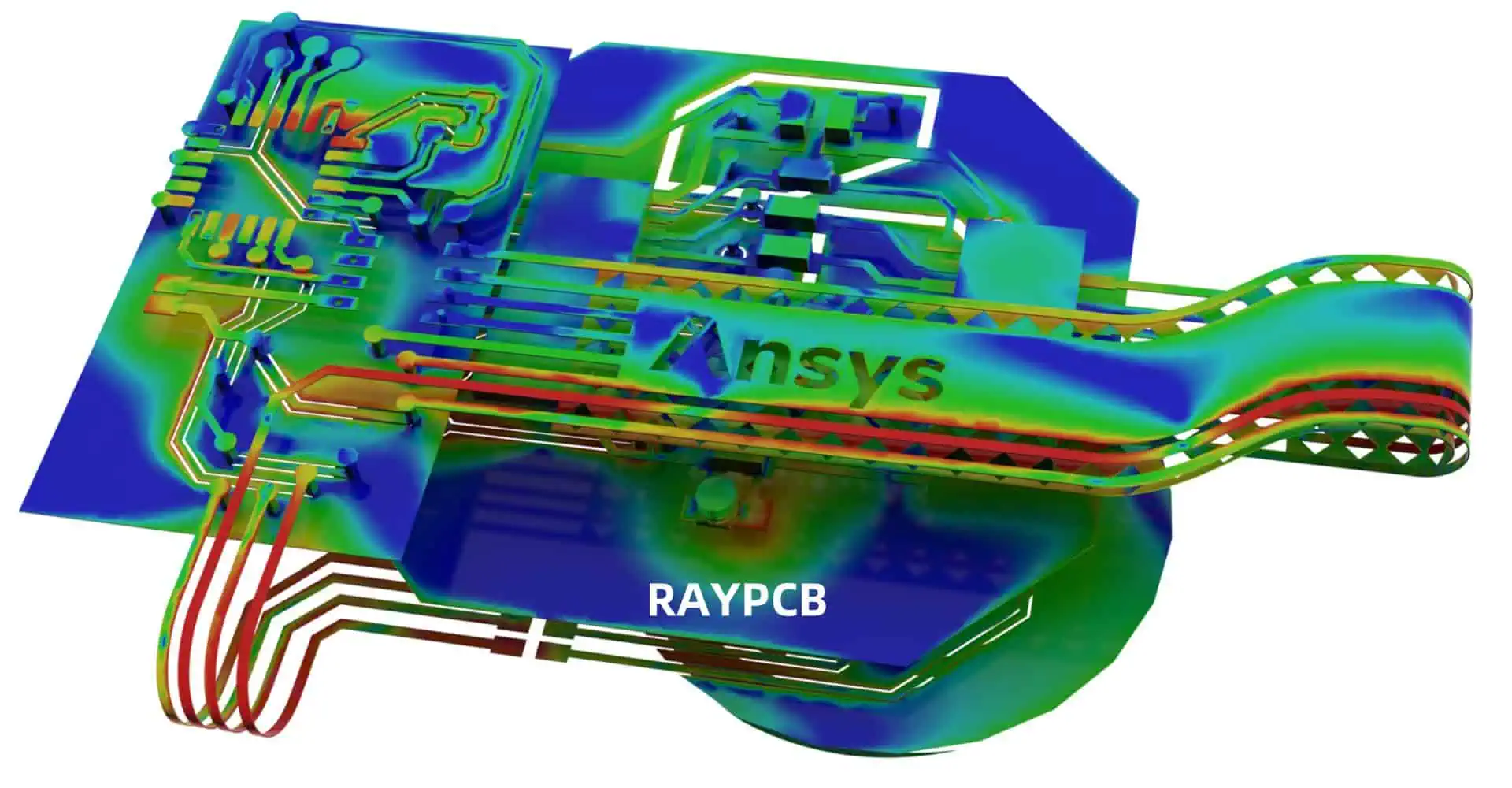
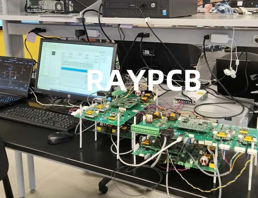
High-Frequency and Signal Integrity Testing
Vector Network Analysis (VNA) for PCB Characterization
Advanced VNA techniques are being used for:
- S-parameter measurements of high-speed PCB traces
- Characterization of differential pairs
- Time-domain reflectometry (TDR) analysis
Near-Field Scanning for EMI/EMC
Near-field scanning systems provide:
- Detailed maps of electromagnetic emissions
- Identification of potential EMI sources on PCBs
- Validation of EMI mitigation strategies
Reliability and Environmental Testing
Highly Accelerated Life Testing (HALT)
HALT chambers subject PCBs to extreme conditions to:
- Identify design weaknesses rapidly
- Determine operational limits
- Improve overall product reliability
In-Situ Monitoring During Environmental Testing
Advanced sensors and data logging systems allow for:
- Real-time monitoring of PCB performance during environmental stress
- Correlation of environmental conditions with failure modes
- More accurate prediction of product lifespan
Integration of Test and Measurement Data
Industry 4.0 and Smart Factory Integration
Modern PCB test and measurement systems are being integrated into smart factory environments, enabling:
- Real-time data collection and analysis
- Predictive maintenance of test equipment
- Adaptive manufacturing based on test results
Big Data Analytics for Test Results
Advanced analytics techniques are being applied to vast amounts of test data to:
- Identify trends and patterns in defects
- Optimize test sequences and coverage
- Predict potential quality issues before they occur
Digital Twin Technology
Digital twins of PCBs and assembly lines are being used to:
- Simulate and optimize test processes
- Predict the impact of design changes on testability
- Improve overall manufacturing efficiency
Comparison of Traditional and Emerging Test Techniques
| Aspect | Traditional Techniques | Emerging Techniques | Key Advantages of Emerging Techniques |
| Optical Inspection | 2D AOI | 3D AOI with AI | Improved defect detection, reduced false positives |
| X-ray Inspection | 2D X-ray | Digital Tomosynthesis with AI | Better inspection of hidden joints, automated analysis |
| Electrical Testing | In-Circuit Test (ICT) | Flying Probe with Thermal Imaging | Increased flexibility, correlation of electrical and thermal issues |
| Signal Integrity | Time Domain Reflectometry | Advanced VNA Techniques | More comprehensive high-frequency characterization |
| Reliability Testing | Thermal Cycling | HALT with In-Situ Monitoring | Faster identification of weaknesses, real-time performance data |
| Data Analysis | Statistical Process Control | Big Data Analytics and AI | Predictive quality control, trend analysis across multiple parameters |
Challenges and Future Directions
Challenges in Implementing New Test Techniques
- High initial investment costs
- Need for specialized training and expertise
- Integration with existing manufacturing processes
- Balancing increased test coverage with production throughput
Future Directions in PCB Test and Measurement
Artificial Intelligence and Machine Learning
AI and ML are expected to play an increasingly important role in:
- Automated defect classification and prediction
- Optimization of test sequences and coverage
- Predictive maintenance of test equipment
Non-Contact and Non-Destructive Testing
Advancements in technologies such as:
- Terahertz imaging for internal PCB inspection
- Acoustic microscopy for solder joint analysis
- Advanced electromagnetic field scanning
Integration of Design for Test (DFT) and Test and Measurement
Closer collaboration between PCB designers and test engineers to:
- Implement built-in self-test features
- Optimize PCB layouts for testability
- Reduce overall test time and cost
Quantum Sensing for Ultra-Precise Measurements
Emerging quantum technologies may enable:
- Extremely sensitive magnetic field measurements
- Ultra-precise time and frequency measurements for high-speed circuits
- Novel approaches to defect detection at the atomic scale
Conclusion
The field of PCB test and measurement is undergoing rapid transformation, driven by the increasing complexity of electronic designs and the need for higher quality and reliability. Emerging techniques in optical and X-ray inspection, electrical testing, signal integrity analysis, and reliability testing are pushing the boundaries of what’s possible in PCB quality assurance.
The integration of artificial intelligence, big data analytics, and smart factory concepts is revolutionizing how test data is collected, analyzed, and utilized. These advancements not only improve the accuracy and efficiency of PCB testing but also contribute to overall manufacturing optimization and product innovation.
As the electronics industry continues to evolve, PCB test and measurement techniques will play a crucial role in enabling the next generation of electronic devices. The challenges of implementing these new technologies are significant, but the potential benefits in terms of improved quality, reduced time-to-market, and enhanced product performance make them essential for companies looking to stay competitive in the fast-paced world of electronics manufacturing.
The future of PCB test and measurement lies in the seamless integration of advanced sensing technologies, artificial intelligence, and comprehensive data analysis. As these technologies mature and become more accessible, they will undoubtedly shape the landscape of electronics manufacturing, driving innovation and ensuring the reliability of increasingly complex electronic systems.
Frequently Asked Questions (FAQ)
- Q: How do emerging PCB test techniques improve upon traditional methods? A: Emerging techniques offer several improvements, including higher resolution and accuracy in defect detection, ability to inspect hidden or internal features, faster test times, and integration of multiple test modalities (e.g., electrical and thermal). They also leverage AI and big data analytics to provide predictive insights and optimize the testing process.
- Q: What are the main challenges in implementing new PCB test and measurement techniques? A: The main challenges include high initial investment costs, the need for specialized training and expertise, integration with existing manufacturing processes, and balancing increased test coverage with production throughput. Additionally, there may be challenges in data management and interpretation given the large amounts of data generated by advanced test systems.
- Q: How does artificial intelligence contribute to PCB testing? A: AI contributes to PCB testing in several ways, including enhancing defect detection accuracy in optical and X-ray inspection, automating the analysis of complex test data, optimizing test sequences, predicting potential quality issues, and enabling adaptive testing based on real-time results.
- Q: Are these new test techniques suitable for all types of PCBs? A: While many new techniques offer benefits across a wide range of PCB types, their applicability can vary. High-end techniques may be most beneficial for complex, high-value PCBs where the cost of failure is high. However, as technologies mature and become more cost-effective, they are increasingly being adopted for a broader range of PCB types and production volumes.
- Q: How do new PCB test techniques address the challenges of testing high-frequency and high-speed circuits? A: New techniques address high-frequency and high-speed circuit challenges through advanced vector network analysis for accurate S-parameter measurements, near-field scanning for EMI/EMC analysis, and improved time-domain reflectometry for signal integrity testing. These methods provide more detailed characterization of high-speed traces, differential pairs, and overall PCB performance at higher frequencies.