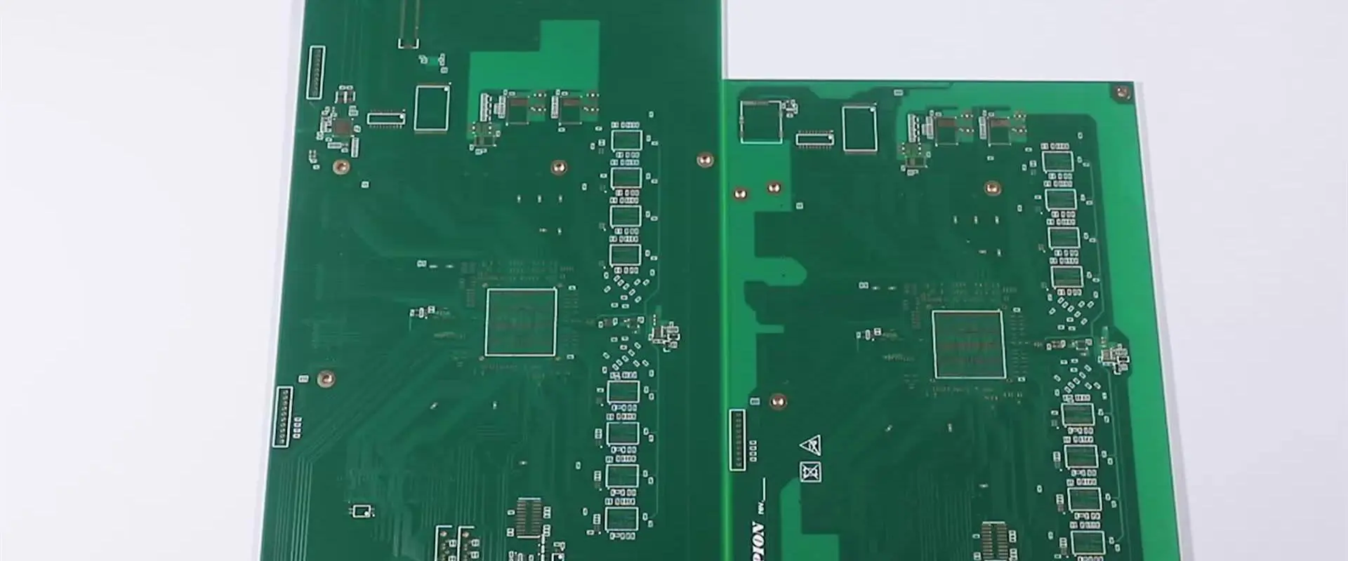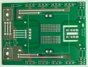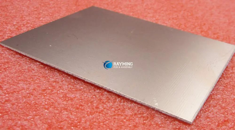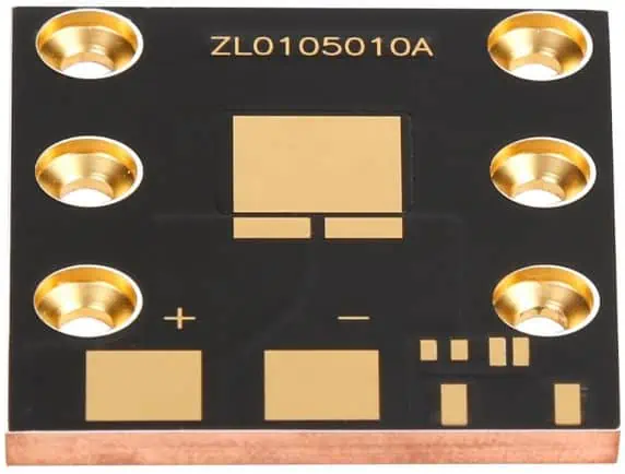
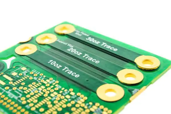
10 Oz Copper PCB
Board Thickness: 2.0mm
Surface Process: ENIG
Solder Mask : Green
Legend :White
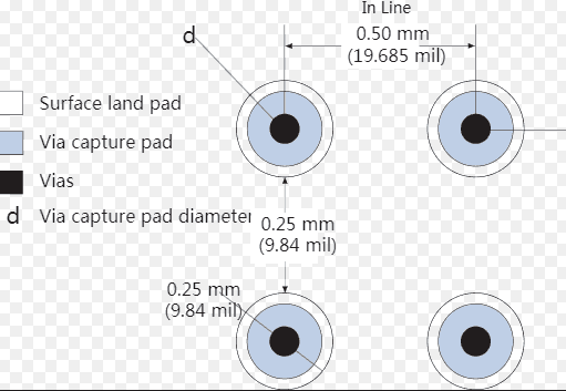
General Guideline for Min Spacing by Copper Weight
Cu Weight Min Recommended Space between Copper Feature
10 OZ 38mil ( 0.965mm )
Introduction
As electronics become more powerful and compact, demand rises for ultra-high performance printed circuit boards (PCBs) using 10 oz copper thickness to handle increasing currents and heat loads. However, reliably producing 10 oz copper multilayer boards poses immense fabrication challenges. Selecting an experienced PCB manufacturer with proven expertise in 10 oz technology is key to ensuring flawless quality and performance.
This article provides electronics engineers an overview of 10 oz copper PCB capabilities, manufacturing process requirements, quality benchmarks, and the benefits of partnering with a high quality 10 oz board supplier.
What is a 10 Oz Copper PCB?
PCB copper thickness is designated in ounces per square foot (oz/ft2). This refers to the weight of copper foil in one square foot of board area, excluding the fiberglass dielectric weight. Some standard thicknesses are:
- 1 oz – 1 oz/ft2 (35 μm)
- 2 oz – 2 oz/ft2 (70 μm)
- 4 oz – 4 oz/ft2 (140 μm)
- 6 oz – 6 oz/ft2 (210 μm)
- 10 oz – 10 oz/ft2 (350 μm)
So a 10 oz copper PCB has 10 ounces of copper foil per square foot on each metal layer. In terms of thickness, 10 oz copper equals approximately:
- 350 μm (0.35 mm)
- 14 mils
This extreme copper thickness enables unmatched power handling, thermal management and reliability.
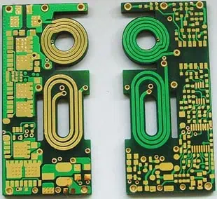
Advantages of 10 oz Copper PCBs
Some benefits of 10 oz copper PCB technology over standard 1-6 oz copper include:
- Highest current capacity – Ability to sustain very high current loads without overheating due to enormous copper cross-section.
- Lowest electrical losses – Extremely low resistive losses due to thick, short traces. Maximizes electrical efficiency.
- Finest thermal conduction – The thick copper acts as a heat spreader keeping components cool.
- Superior shielding – Near total EMI shielding from thick uninterrupted copper planes.
- Extreme reliability – Highly resistant to thermal cycling, electromigration and physical stresses over decades.
- Low voltage drop – Minimal voltage loss along power distribution paths due to low resistivity.
- Dense integration – Integrate complex high power components in compact footprint.
- High power density – More total power can flow through a given PCB area.
10 oz copper provides the ultimate in performance for the most demanding power electronic systems requiring robustness and miniaturization.
Challenges in 10 oz PCB Manufacturing
While providing immense benefits, fabricating quality 10 oz copper PCBs poses substantial production challenges:
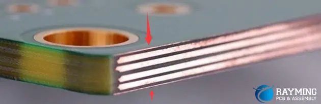
- Registration – Accumulated tolerance of ultra-thick 10 oz layers can result in layer misalignment.
- Aspect Ratios – Plating high aspect ratio 14:1 drill holes reliably is hugely difficult.
- Lamination Voids – Bonding layers without any voids or resin starvation areas is challenging.
- Surface Finish – Achieving uniform plating thickness on coarse foil surfaces requires precision process control.
- Line Resolution – Defining very fine 1-2 mil lines on the rough matte foil side can be problematic.
- Layer Bonding – High peel strengths are needed between layers to avoid any delamination risk.
- Via Filling – Complete pore-free copper fill of high aspect through holes requires special plating regimes.
- Drilling – Straight vertical holes with minimal taper require specialized bits and rigid machinery.
- Hole Wall Quality – Smooth, resin-rich hole walls prevent plating pullaway defects.
- Panel Stress – Accumulated stresses during fabrication must be minimized to prevent any warpage.
These factors demand advanced manufacturing capabilities to produce flawless 10 oz boards.
Key 10 oz PCB Manufacturing Capabilities
To reliably fabricate high quality 10 oz copper multilayer PCBs, manufacturers must demonstrate several advanced capabilities:
- Registration accuracy – Within 0.10mm to avoid any alignment issues between layers.
- Plating Aspect Ratios – Void-free copper plating of at least 12:1 aspect through holes.
- **Lamination – **No filler starvation areas and precise pressure control during bonding.
- Etching – Fine line capability down to 1 mil line/space.
- Hole Wall Quality – Excellent resin coating of drilled hole walls.
- Surface Finish – Highly uniform thick gold plating over coarse copper.
- Peel Strength – Interlaminar peel strength over 9 N/mm to prevent delamination.
- Via Filling – Pore-free copper plating fill on high aspect through holes.
- Drilling – Straight vertical holes through 14 mil copper with minimal taper.
- Panel Flatness – Thickness variation under 5% and minimal bow or twist.
- Reliability Testing – Extensive thermal shock/cycling, vibration, flexure and other rigorous testing.
Process Control – Stringent process monitoring, change control and corrective action systems.
These parameters indicate whether a PCB company has the technical maturity to manufacture 10 oz boards reliably.
Benefits of Selecting a Premier 10 oz PCB Manufacturer
Choosing an established PCB company with proven expertise in 10 oz copper provides key advantages:
- Mitigate Technology Risk – Avoid initial issues during 10 oz adoption by leveraging robust qualified processes.
- Accelerate Time-to-Market – Get products to market faster through on-demand prototypes and rapid scaling.
- Increase Performance Margins – Achieve maximum possible electrical and thermal performance.
- Ensure Reliability – Robust process and quality standards deliver ultra-reliable 10 oz boards.
- Control Costs – Leverage accumulated manufacturing learning and economies of scale.
- Simplify Logistics – Single partner for prototypes through volume production.
- Strategic Alignment – Collaborate on design solutions and technology roadmap.
For companies looking to harness the tremendous benefits of 10 oz copper PCBs, finding the right manufacturing partner provides immense strategic value in capabilities, time-to-market, performance and costs.
Frequently Asked Questions
Q1. Does 10 oz copper affect signal integrity at high speeds?
The extremely low losses and matched impedances of 10 oz copper traces aid signal integrity for high speed designs. Effects like reflections and EMI are minimized.
Q2. What is the minimum hole size possible with 10 oz copper PCBs?
With laser drilling, holes down to 0.15mm diameter with 12:1 aspect ratio can be reliably achieved with 10 oz copper stacks.
Q3. Can components be soldered onto 10 oz copper boards?
Yes, the soldering process works very well on 10 oz copper PCBs. The high copper thermal mass helps prevent excessive heating of components.
Q4. Does 10 oz copper alter PCB flex or vibration response?
Some damping effect may occur with 10 oz boards. But the copper and laminate mechanical properties remain similar.
Q5. Is the cost much higher for 10 oz versus 6 oz copper PCBs?
The material cost increase is moderate. But advanced fabrication capabilities required do make 10 oz PCBs cost more than 6 oz boards with similar layer counts.
Conclusion
While enabling unprecedented capabilities, reliably producing quality 10 oz copper PCBs is extremely demanding. Partnering with an established manufacturer that has mastered the sophisticated processes and controls required for 10 oz multilayer boards allows maximizing yield, performance and long-term reliability. For electronics companies looking to leverage thick copper technology in new product designs, selecting a precision high quality PCB partner with proven expertise mitigates adoption risks and paves the path to successful deployment.