How to Choose a Professional PCB Prototype Assembler

PCB prototype assembly suppliers

Selecting the right PCB prototype assembler is a critical decision that can significantly impact your product development timeline, quality, and overall project success. With numerous options available in the market, from local shops to international manufacturers, making an informed choice requires careful consideration of multiple factors. This comprehensive guide will walk you through the essential criteria and considerations for choosing a professional PCB prototype assembler that best fits your specific needs.

Understanding Your Project Requirements

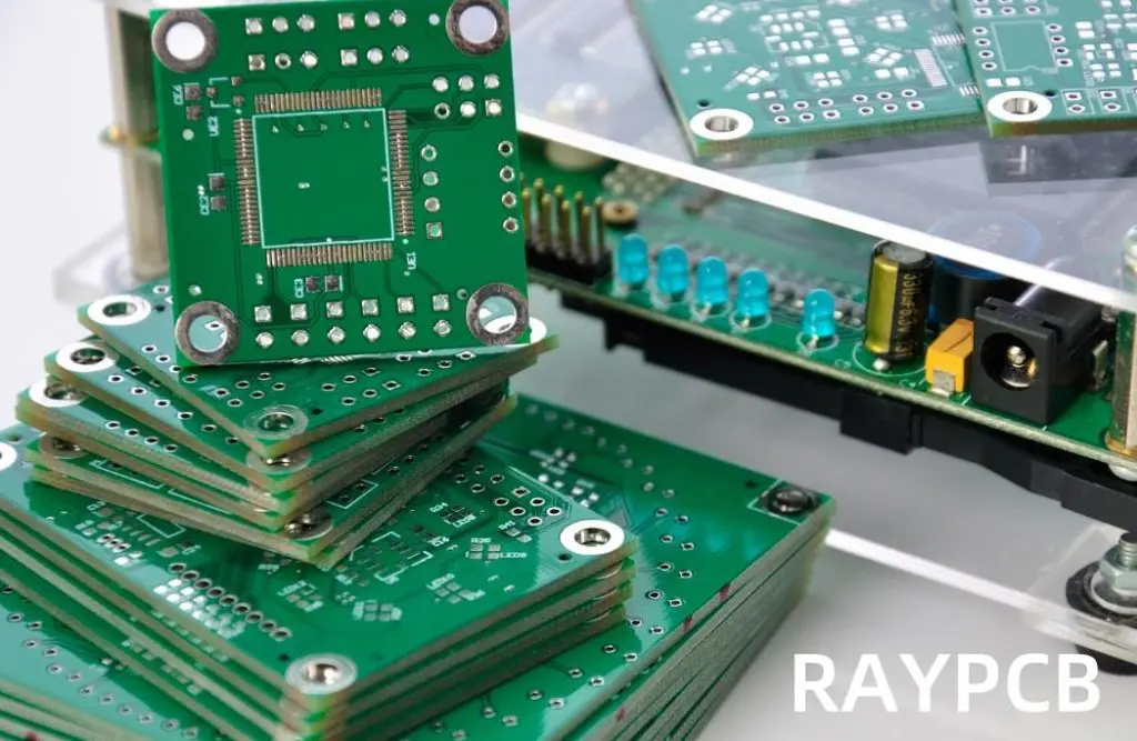
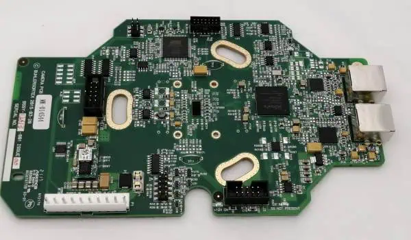
Before evaluating potential assemblers, clearly define your project specifications and requirements. Consider the complexity of your PCB design, including the number of layers, component density, and types of components you’ll be using. Surface-mount technology (SMT) components, through-hole components, and mixed assemblies each present different challenges and require specific equipment and expertise. Document your expected quantities, turnaround time requirements, and quality standards. Understanding whether you need a one-time prototype or ongoing small-batch production will help narrow down suitable candidates.

Technical Capabilities and Equipment

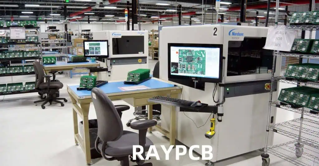
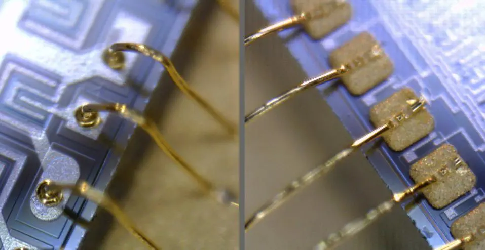
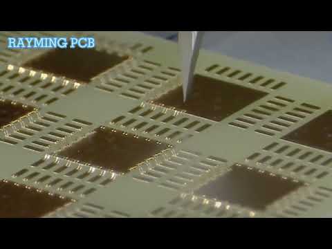
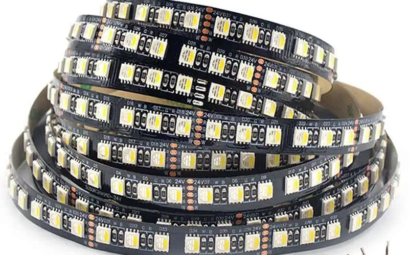
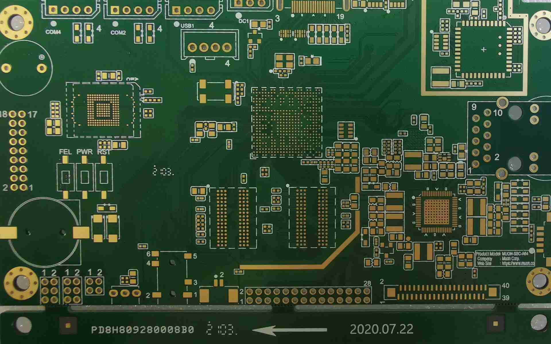
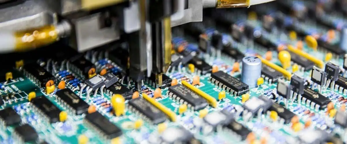
A professional PCB prototype assembler should possess modern, well-maintained equipment capable of handling your specific requirements. Look for facilities equipped with advanced pick-and-place machines, reflow ovens, wave soldering equipment, and inspection systems. The assembler should have experience with your component types, particularly if you’re using specialized parts like BGAs (Ball Grid Arrays), QFNs (Quad Flat No-leads), or high-frequency components. Inquire about their minimum component sizes they can handle, as modern designs often incorporate 0201 or even smaller components.

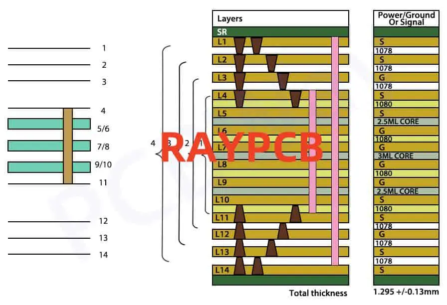
Ask about their PCB handling capabilities, including minimum and maximum board sizes, thickness ranges, and any special substrate materials they can work with. If your design includes rigid-flex PCBs or requires specific environmental considerations, ensure the assembler has relevant experience and equipment. The facility should also have proper anti-static controls, clean room environments where necessary, and appropriate storage conditions for moisture-sensitive components.

Quality Control and Certifications

Quality assurance is paramount when selecting a PCB prototype assembler. Look for facilities with relevant certifications such as ISO 9001, IPC-A-610 (Acceptability of Electronic Assemblies), and IPC-J-STD-001 (Requirements for Soldered Electrical and Electronic Assemblies). These certifications indicate adherence to industry standards and commitment to quality processes.

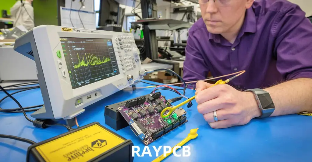
Inquire about their inspection procedures, which should include automated optical inspection (AOI), in-circuit testing (ICT), and functional testing capabilities. The assembler should provide detailed inspection reports and be willing to discuss their defect rates and quality metrics. A professional assembler will have documented procedures for handling non-conforming products and implementing corrective actions.

Experience and Expertise

Experience in your specific industry or application area can be invaluable. An assembler familiar with automotive electronics will understand different requirements than one specializing in consumer electronics or medical devices. Review their portfolio and ask for case studies or references from similar projects. Experienced assemblers can often provide valuable design feedback and suggest improvements that can enhance manufacturability and reduce costs.

Consider their engineering support capabilities. A good prototype assembler should offer design for manufacturing (DFM) reviews, helping identify potential assembly issues before production begins. They should be able to provide feedback on component selection, footprint optimization, and assembly processes that could improve your design’s reliability and manufacturability.

Communication and Customer Service

Effective communication is crucial throughout the prototype assembly process. Evaluate how responsive and clear the assembler’s communication is during initial inquiries. They should be willing to discuss your project in detail, provide accurate quotes, and explain their processes clearly. Look for assemblers who assign dedicated project managers or engineers to your account, ensuring consistent communication and accountability.

The assembler should provide regular updates on project progress and be accessible for questions or concerns. They should also be proactive in communicating any issues or potential delays, allowing you to make informed decisions about project adjustments.

Turnaround Time and Flexibility

Prototype development often operates under tight schedules, making turnaround time a critical factor. Evaluate each assembler’s standard lead times and their ability to accommodate rush orders when necessary. However, be cautious of assemblers who promise unrealistically fast turnaround times, as this may come at the expense of quality.

Consider their flexibility in handling design changes or component substitutions that might arise during the prototype phase. A good assembler should be able to accommodate reasonable modifications without significant delays or excessive charges. They should also have established relationships with component suppliers to help source hard-to-find parts or provide suitable alternatives.

Cost Considerations and Pricing Structure

While cost shouldn’t be the only deciding factor, it’s certainly important for most projects. Request detailed quotes from multiple assemblers, ensuring they include all relevant costs such as setup fees, component procurement, assembly labor, testing, and shipping. Be wary of quotes that seem significantly lower than others, as they may not include all necessary services or may compromise on quality.

Consider the total cost of ownership, including potential rework costs, shipping expenses, and the value of time saved through efficient processes. Some assemblers offer package deals for prototypes that include multiple iterations or small production runs, which can provide better overall value for ongoing projects.

Component Procurement and Supply Chain Management

Many prototype assemblers offer component procurement services, which can simplify your project management and potentially reduce costs through their supplier relationships. Evaluate their component sourcing capabilities, including their supplier network, inventory management systems, and ability to source obsolete or hard-to-find components.

Inquire about their policies regarding excess components and how they handle component returns or credits. Some assemblers maintain consignment inventory for frequently used components, which can reduce lead times for future orders. They should also have processes for verifying component authenticity and quality, particularly important in today’s market with counterfeit components.

Location and Logistics

Consider the geographic location of the assembler relative to your operations. Local or regional assemblers may offer advantages in communication, site visits, and shipping costs, while offshore options might provide cost savings for larger quantities. Evaluate their shipping options, packaging methods, and ability to meet any specific delivery requirements you might have.

For international assemblers, consider factors such as time zone differences, language barriers, customs procedures, and potential supply chain disruptions. Some projects may benefit from the cost advantages of offshore assembly, while others requiring close collaboration or quick iterations may be better served by local providers.

Making the Final Decision

After evaluating potential assemblers against these criteria, create a decision matrix weighing the factors most important to your specific project. Consider requesting samples or starting with a small trial project to evaluate their actual performance before committing to larger orders. The lowest-cost option isn’t always the best choice when considering the total impact on your project timeline and success.

Remember that building a long-term relationship with a reliable PCB prototype assembler can provide significant benefits for future projects, including improved understanding of your requirements, streamlined processes, and potentially better pricing for ongoing work.

Choosing the right PCB prototype assembler requires careful evaluation of multiple factors beyond just price and delivery time. By thoroughly assessing technical capabilities, quality systems, experience, and service levels, you can select a partner who will contribute to your project’s success and support your ongoing development needs. Take the time to properly evaluate your options, as this decision will significantly impact your prototype development experience and outcomes.

Factors Affecting the Cost of Manufacturing Printed Circuit Boards at RayMing PCB

multilayer pcb manufacturers

The cost of manufacturing printed circuit boards (PCBs) is influenced by numerous interconnected factors that directly impact both production efficiency and final pricing. At RayMing PCB, understanding these cost drivers is essential for optimizing manufacturing processes, maintaining competitive pricing, and delivering value to customers. This comprehensive analysis examines the primary factors that affect PCB manufacturing costs and their implications for the production workflow.

Design Complexity and Specifications

The complexity of PCB design serves as one of the most significant cost determinants in manufacturing. Simple single-layer boards with basic routing require minimal processing time and fewer manufacturing steps, resulting in lower costs. However, as designs become more sophisticated with multiple layers, dense component placement, and intricate routing patterns, manufacturing complexity increases exponentially.

Multi-layer PCBs require additional lamination processes, precise layer alignment, and specialized drilling techniques for via connections. Each additional layer increases material costs and processing time, while also demanding higher precision in manufacturing equipment. Complex designs with fine-pitch components, such as ball grid arrays (BGAs) or chip-scale packages (CSPs), require advanced manufacturing capabilities and stricter quality control measures, which translate directly into higher production costs.

The trace width and spacing specifications also significantly impact manufacturing costs. Boards requiring fine-line technology with trace widths below 0.1mm demand specialized etching equipment and more precise process control. These requirements necessitate slower production speeds and higher reject rates, both of which increase overall manufacturing costs.

Material Selection and Quality

Material costs represent a substantial portion of total PCB manufacturing expenses. The choice of substrate material dramatically affects both performance characteristics and production costs. Standard FR-4 materials offer cost-effective solutions for general applications, while specialized materials like Rogers, Taconic, or ceramic substrates command premium prices due to their enhanced electrical properties and manufacturing requirements.

High-frequency applications often require low-loss dielectric materials that maintain signal integrity across broad frequency ranges. These specialized materials not only cost more to procure but also require modified processing parameters and handling procedures during manufacturing. Similarly, flexible PCB materials and rigid-flex constructions involve different lamination processes and specialized tooling, contributing to increased manufacturing costs.

The copper weight specification directly influences material costs, as heavier copper requires thicker plating processes and affects the overall board thickness. Heavy copper PCBs (2oz and above) require modified etching parameters and longer processing times, while also demanding more robust handling equipment throughout the manufacturing process.

Production Volume and Economy of Scale

Manufacturing volume plays a crucial role in determining per-unit costs through economy of scale principles. Large production runs enable manufacturers to amortize setup costs, tooling expenses, and process optimization efforts across numerous units, significantly reducing individual board costs. Small prototype runs or low-volume production carries higher per-unit costs due to the fixed setup expenses being distributed across fewer pieces.

Batch processing efficiency also impacts costs, as manufacturers can optimize equipment utilization and reduce changeover times when producing larger quantities of identical boards. The ability to maintain consistent production parameters across extended runs improves yield rates and reduces waste, contributing to overall cost reduction.

Manufacturing Process Requirements

The specific manufacturing processes required for each PCB design significantly influence production costs. Standard through-hole drilling operations are relatively inexpensive compared to micro-via drilling, which requires laser drilling equipment and specialized processing techniques. Blind and buried vias add complexity to the manufacturing process, requiring sequential lamination and multiple drilling operations.

Surface finish requirements also affect manufacturing costs. Standard HASL (Hot Air Solder Leveling) finishes are cost-effective for most applications, while premium finishes like ENIG (Electroless Nickel Immersion Gold), OSP (Organic Solderability Preservative), or immersion silver require additional processing steps and specialized chemistry, increasing overall costs.

Controlled impedance requirements necessitate precise material selection, stack-up design, and process control throughout manufacturing. Achieving consistent impedance values requires careful monitoring of dielectric thickness, copper weight, and trace geometry, all of which add to manufacturing complexity and cost.

Quality Standards and Testing Requirements

Different quality standards and testing requirements significantly impact manufacturing costs. Consumer electronics applications may require basic electrical testing and visual inspection, while aerospace, medical, or military applications demand extensive testing protocols including microsectioning, thermal cycling, and comprehensive electrical characterization.

IPC class standards directly influence manufacturing costs, with Class 3 requirements (high-reliability applications) demanding stricter process controls, enhanced inspection procedures, and lower acceptable defect rates compared to Class 1 or Class 2 standards. Higher quality standards typically result in lower yields and increased inspection time, both contributing to higher manufacturing costs.

Equipment and Facility Considerations

The sophistication of manufacturing equipment required for specific PCB designs affects production costs through equipment depreciation, maintenance, and operational expenses. Advanced features like HDI (High Density Interconnect) technology require state-of-the-art drilling and imaging equipment, while standard PCB manufacturing can utilize more conventional machinery.

Clean room requirements for certain applications add facility costs through environmental control systems, specialized air filtration, and contamination prevention measures. These facility upgrades represent significant capital investments that must be recovered through manufacturing pricing.

Labor and Operational Costs

Skilled labor requirements vary significantly based on PCB complexity and quality standards. Complex assemblies requiring manual inspection, rework, or specialized handling demand experienced technicians, while automated processes can utilize less specialized labor. Geographic location also influences labor costs, with facilities in different regions experiencing varying wage rates and benefit costs.

Training requirements for new processes or technologies represent additional operational expenses that influence overall manufacturing costs. Maintaining certifications for quality standards like ISO 9001, AS9100, or IPC requirements involves ongoing training and documentation efforts.

Supply Chain and Logistics Factors

Raw material availability and supplier relationships significantly impact manufacturing costs through pricing stability and supply chain efficiency. Long-term supplier partnerships often provide cost advantages through volume discounts and preferential pricing arrangements, while spot market purchases typically carry premium pricing.

Inventory management strategies affect carrying costs and cash flow requirements. Just-in-time inventory approaches can reduce carrying costs but may increase material prices due to smaller purchase quantities and reduced negotiating power with suppliers.

Market Conditions and Competition

Industry-wide demand fluctuations influence material costs and manufacturing capacity utilization. During high-demand periods, material costs typically increase while manufacturing lead times extend, potentially affecting pricing strategies. Conversely, periods of reduced demand may provide opportunities for cost reduction through supplier negotiations and improved capacity utilization.

Competitive pressure within the PCB manufacturing industry drives continuous improvement in manufacturing efficiency and cost reduction initiatives. Companies must balance competitive pricing with investment in advanced manufacturing capabilities to maintain market position.

Technology Advancement and Innovation

Emerging technologies and manufacturing process improvements offer opportunities for cost reduction while enabling new capabilities. Investment in advanced equipment and process optimization can reduce long-term manufacturing costs while improving quality and capability.

However, technology adoption requires significant capital investment and workforce training, representing substantial upfront costs that must be amortized over future production volumes. The timing of technology adoption decisions significantly impacts both short-term costs and long-term competitive positioning.

Conclusion

The cost of manufacturing printed circuit boards at RayMing PCB results from the complex interaction of multiple factors ranging from design specifications and material selection to production volume and quality requirements. Understanding these cost drivers enables informed decision-making throughout the design and manufacturing process, ultimately leading to optimized solutions that balance performance requirements with cost considerations.

Successful PCB manufacturing requires careful consideration of all these factors during the design phase, as early decisions significantly impact final manufacturing costs. By working closely with customers to understand application requirements and constraints, RayMing PCB can optimize manufacturing approaches to deliver high-quality products at competitive prices while maintaining the flexibility to adapt to changing market conditions and technological advances.

Factors Affecting the Longevity of Copper Bond

Introduction

Copper bonding represents a critical technology in modern electronics manufacturing, particularly in semiconductor packaging, printed circuit boards (PCBs), and advanced interconnect systems. The longevity of copper bonds directly impacts the reliability, performance, and lifespan of electronic devices. Understanding the multifaceted factors that influence copper bond durability is essential for engineers, manufacturers, and quality control professionals working in electronics, automotive, aerospace, and telecommunications industries.

The integrity of copper bonds determines whether electronic systems will function reliably over their intended operational lifetime, making this topic crucial for applications ranging from consumer electronics to mission-critical aerospace systems. This comprehensive analysis examines the various factors that affect copper bond longevity, providing insights into failure mechanisms and strategies for optimization.

YouTube video

Environmental Factors

Temperature Effects

Temperature stands as one of the most significant factors affecting copper bond longevity. Copper’s thermal expansion coefficient differs from many substrate materials, creating thermal stress during temperature cycling. High temperatures accelerate various degradation mechanisms, including diffusion processes, oxidation reactions, and intermetallic compound formation.

Thermal cycling, particularly in automotive and aerospace applications, subjects copper bonds to repeated expansion and contraction cycles. These mechanical stresses can lead to fatigue cracking, delamination, and eventual bond failure. The severity of thermal stress depends on the temperature range, cycling frequency, and the thermal expansion mismatch between copper and adjacent materials.

Low-temperature environments can also impact copper bond longevity by altering material properties and potentially causing brittle fracture modes. The temperature coefficient of resistance changes in copper can affect electrical performance and contribute to localized heating effects that further stress the bond interface.

Humidity and Moisture

Moisture presents a significant threat to copper bond integrity through several mechanisms. Water vapor can penetrate packaging materials and reach bond interfaces, where it facilitates corrosion processes and degrades adhesion. High humidity environments accelerate electrochemical corrosion, particularly in the presence of ionic contaminants.

Moisture can also cause swelling in organic substrates and encapsulants, creating mechanical stress on copper bonds. The hygroscopic nature of many packaging materials means that humidity absorption is often irreversible, leading to permanent dimensional changes that stress bond interfaces over time.

Chemical Environment

The chemical environment surrounding copper bonds significantly influences their longevity. Exposure to corrosive gases, acids, bases, or organic solvents can directly attack copper surfaces or interfacial materials. Sulfur-containing compounds are particularly problematic, as they can form copper sulfides that compromise electrical conductivity and mechanical integrity.

Industrial environments often contain airborne contaminants that can deposit on copper surfaces and initiate corrosion processes. Salt spray in marine environments represents an extreme case where chloride ions can rapidly degrade copper bonds through pitting corrosion and crevice corrosion mechanisms.

Material Properties and Composition

Copper Purity and Grain Structure

The purity of copper used in bonding applications directly affects longevity. High-purity copper generally exhibits superior corrosion resistance and mechanical properties. However, the presence of specific alloying elements can sometimes improve performance characteristics such as strength and thermal stability.

Grain structure in copper affects mechanical properties, with finer grain structures typically providing higher strength but potentially altered diffusion characteristics. The grain boundary density and orientation can influence how stress concentrates within the copper and affects crack propagation behavior.

Surface Preparation and Cleanliness

Surface preparation quality critically determines initial bond strength and long-term reliability. Contamination from oils, oxides, or process residues can create weak interfaces that fail prematurely. Surface roughness affects the actual contact area and can influence stress concentration patterns.

Proper surface cleaning and activation processes ensure optimal adhesion between copper and mating surfaces. The use of appropriate flux materials, plasma cleaning, or chemical etching can significantly improve bond quality and longevity.

Substrate Compatibility

The choice of substrate material profoundly affects copper bond longevity through thermal expansion matching, chemical compatibility, and interfacial adhesion characteristics. Ceramic substrates offer excellent thermal stability but may have thermal expansion mismatches with copper. Organic substrates provide better thermal expansion matching but may be more susceptible to environmental degradation.

The surface energy and chemical composition of substrates determine how well copper bonds will adhere initially and maintain adhesion over time. Surface treatments and primers can improve compatibility but add complexity to the manufacturing process.

Processing Parameters

Bonding Temperature and Pressure

The temperature and pressure used during the bonding process establish the initial bond quality and microstructure. Insufficient temperature may result in incomplete diffusion and weak bonds, while excessive temperature can cause grain growth, intermetallic formation, or substrate degradation.

Bonding pressure affects the intimate contact between surfaces and can influence the elimination of voids and contaminants. However, excessive pressure may cause deformation that creates residual stresses or damages fragile substrates.

Process Atmosphere Control

The atmosphere during bonding significantly affects oxidation behavior and surface cleanliness. Inert atmospheres prevent oxidation but require careful control to maintain effectiveness. Reducing atmospheres can help clean surfaces but may affect other materials in the assembly.

Vacuum processing eliminates atmospheric contaminants but requires specialized equipment and may affect outgassing from organic materials. The choice of process atmosphere must balance copper bond quality with other manufacturing requirements.

Cooling Rate and Thermal History

The cooling rate after bonding affects the final microstructure and residual stress state in copper bonds. Rapid cooling can create high thermal stresses due to thermal expansion mismatches, while slow cooling may allow stress relaxation but could promote unwanted phase transformations.

The complete thermal history during processing, including any subsequent thermal treatments, influences the evolution of microstructure and stress states that determine long-term reliability.

Mechanical Stress Factors

Residual Stresses

Residual stresses develop during processing due to thermal expansion mismatches, phase transformations, and mechanical constraints. These stresses remain in the copper bond structure and can accelerate failure mechanisms under service conditions.

Compressive residual stresses in copper can be beneficial by opposing tensile service loads, while tensile residual stresses are generally detrimental as they add to service loads and can promote crack initiation and propagation.

External Loading Conditions

Service loads including vibration, shock, bending, and thermal cycling create additional stresses in copper bonds. The frequency and amplitude of these loads determine their impact on bond longevity through fatigue mechanisms.

Static loads can cause stress relaxation and creep in copper bonds, particularly at elevated temperatures. The time-dependent nature of these phenomena means that bonds may gradually weaken even under constant load conditions.

Design Considerations

The geometric design of copper bonds significantly affects stress distribution and concentration. Sharp corners, abrupt thickness changes, and high aspect ratios can create stress concentrations that reduce bond longevity.

Proper design practices including filleting, gradual transitions, and stress relief features can significantly improve copper bond reliability. The overall structural design must consider load paths and how forces are transmitted through the copper bond interface.

Electrical Factors

Current Density and Joule Heating

High current densities in copper bonds generate Joule heating that can create thermal gradients and temperature excursions beyond design limits. This localized heating can accelerate diffusion processes, promote intermetallic growth, and create thermal stresses.

Electromigration effects at high current densities can cause mass transport in copper conductors, leading to void formation and conductor thinning that compromises both electrical and mechanical integrity.

Voltage Stress and Electrochemical Effects

High voltage gradients across copper bonds can promote electrochemical corrosion processes, particularly in the presence of moisture and ionic contaminants. These electrochemical effects can cause preferential dissolution of copper at certain locations.

Galvanic coupling between copper and dissimilar metals in the presence of electrolytes can create corrosion cells that selectively attack copper bonds. Proper material selection and isolation can minimize these effects.

Quality Control and Testing

Initial Bond Quality Assessment

Non-destructive testing methods including ultrasonic inspection, X-ray imaging, and electrical testing can identify initial defects that may compromise long-term reliability. Pull testing and shear testing provide quantitative measures of initial bond strength.

Statistical process control during manufacturing helps ensure consistent bond quality and can identify process variations that affect longevity. Regular monitoring of key process parameters prevents drift that could degrade bond reliability.

Accelerated Life Testing

Accelerated aging tests using elevated temperature, humidity, thermal cycling, and mechanical stress can predict long-term reliability in reasonable test times. Proper acceleration factors must be established to ensure that test results correlate with actual service performance.

Failure analysis of tested samples provides insights into failure mechanisms and helps validate predictive models for copper bond longevity under various service conditions.

Conclusion

The longevity of copper bonds depends on a complex interplay of environmental, material, processing, mechanical, and electrical factors. Understanding these relationships enables engineers to design more reliable systems and optimize manufacturing processes for enhanced durability.

Successful copper bond implementation requires careful attention to material selection, process control, design optimization, and quality assurance. As electronic systems continue to demand higher performance and reliability, the importance of copper bond longevity will only continue to grow across all application sectors.

Future developments in copper bonding technology will likely focus on advanced materials, improved process control, and better predictive models for long-term reliability assessment. The continued evolution of this technology will enable more robust and durable electronic systems for increasingly demanding applications.

Solution to Make Flexible PCB LED Strip Design Into Reality

Flexible PCB LED strips have revolutionized the lighting industry, offering versatile and customizable lighting solutions for various applications. These innovative products combine the flexibility of thin, bendable circuit boards with the efficiency and brightness of LED technology. This article will explore the process of turning a flexible PCB LED strip design into reality, covering everything from initial concept to final production.

Understanding Flexible PCB LED Strips

What are Flexible PCB LED Strips?

Flexible PCB LED strips are lighting products that consist of a series of LEDs mounted on a flexible printed circuit board. These strips can be bent, twisted, and conform to various shapes, making them ideal for applications where traditional rigid PCBs would be impractical.

Key Components of Flexible PCB LED Strips

  1. Flexible PCB: The base material that provides electrical connections and mechanical support.
  2. LEDs: Light-emitting diodes that produce the actual illumination.
  3. Resistors: Components that control current flow to the LEDs.
  4. Connectors: Allow for easy connection to power sources and other strips.
  5. Adhesive Backing: Enables easy mounting on various surfaces.
  6. Protective Coating: Provides water resistance and durability.

Design Considerations for Flexible PCB LED Strips

Electrical Design

  1. LED Selection: Choose appropriate LEDs based on desired color, brightness, and power consumption.
  2. Circuit Layout: Design the circuit to ensure even current distribution and minimize voltage drop.
  3. Power Management: Calculate power requirements and incorporate necessary components for efficient operation.

Mechanical Design

  1. Flexibility: Determine the required bending radius and design accordingly.
  2. Thickness: Balance flexibility with durability when choosing PCB thickness.
  3. Length and Width: Consider standard sizes and customization options.
  4. Mounting Options: Design for various installation methods (adhesive backing, mounting clips, etc.).

Thermal Management

  1. Heat Dissipation: Incorporate thermal management solutions to prolong LED lifespan.
  2. Material Selection: Choose PCB materials with good thermal conductivity.

Environmental Considerations

  1. IP Rating: Design for appropriate ingress protection based on intended use.
  2. UV Resistance: Select materials that can withstand exposure to sunlight if used outdoors.
  3. Chemical Resistance: Consider potential exposure to cleaning agents or other chemicals.

Manufacturing Process

Step 1: PCB Fabrication

  1. Material Selection: Choose appropriate flexible PCB materials (e.g., polyimide, PET).
  2. Copper Layering: Apply copper foil to the flexible substrate.
  3. Photolithography: Create the circuit pattern using photoresist and etching processes.
  4. Surface Finish: Apply surface treatments (e.g., ENIG, HASL) to protect copper traces.

Step 2: Component Assembly

  1. Solder Paste Application: Apply solder paste to the PCB using a stencil.
  2. Component Placement: Use pick-and-place machines to position LEDs and other components.
  3. Reflow Soldering: Heat the PCB to melt the solder and secure components.
  4. Inspection: Perform automated optical inspection (AOI) to ensure proper assembly.

Step 3: Testing and Quality Control

  1. Electrical Testing: Verify continuity and proper functionality of the LED strips.
  2. Brightness and Color Testing: Ensure consistent light output and color accuracy.
  3. Flexibility Testing: Confirm that the strips can bend to the specified radius without damage.
  4. Environmental Testing: Subject samples to temperature, humidity, and other relevant tests.

Step 4: Finishing and Packaging

  1. Conformal Coating: Apply a protective layer to enhance durability and water resistance.
  2. Cutting and Termination: Cut strips to desired lengths and add end connectors.
  3. Adhesive Application: Apply double-sided adhesive tape to the back of the strips.
  4. Packaging: Package the LED strips in protective materials for shipping.

Overcoming Common Challenges

1. Maintaining Flexibility

Challenge: Ensuring the PCB remains flexible while accommodating necessary components and traces.

Solution:

  • Use ultra-thin PCB materials (e.g., 0.1mm polyimide)
  • Implement careful trace routing to avoid areas of high stress
  • Utilize flexible solder masks and coverlays

2. Thermal Management

Challenge: Dissipating heat from densely packed LEDs on a flexible substrate.

Solution:

  • Incorporate thermal vias to improve heat transfer
  • Use thermally conductive adhesives for better heat dissipation
  • Design with adequate spacing between high-power LEDs

3. Voltage Drop

Challenge: Maintaining consistent brightness along long LED strips due to voltage drop.

Solution:

  • Implement parallel circuit designs to reduce voltage drop
  • Use higher voltage power supplies (e.g., 24V instead of 12V)
  • Incorporate voltage regulators or constant current drivers

4. Water and Dust Resistance

Challenge: Protecting the LED strips from environmental factors without compromising flexibility.

Solution:

  • Apply conformal coatings that remain flexible when cured
  • Design custom silicone or polyurethane encapsulations
  • Use IP-rated connectors and sealing techniques at termination points

Comparison of Flexible PCB Materials for LED Strips

MaterialFlexibilityTemperature ResistanceCostDurability
PolyimideExcellentHigh (up to 200ยฐC)HighExcellent
PETGoodModerate (up to 105ยฐC)LowGood
PENVery GoodGood (up to 150ยฐC)ModerateVery Good
PTFEExcellentVery High (up to 260ยฐC)Very HighExcellent
FPCGoodModerate (up to 105ยฐC)ModerateGood

Design Optimization Techniques

1. Simulation and Modeling

Utilize advanced simulation software to model:

  • Electrical performance
  • Thermal behavior
  • Mechanical stress

This helps identify potential issues before physical prototyping.

2. Modular Design

Implement a modular approach to:

  • Facilitate easier customization
  • Simplify manufacturing and inventory management
  • Enable quick repairs and replacements

3. Smart Integration

Incorporate intelligent features such as:

  • Built-in controllers for dynamic lighting effects
  • Sensors for automatic brightness adjustment
  • Wireless connectivity for remote control

4. Material Innovation

Explore cutting-edge materials:

  • Stretchable conductive inks
  • Novel flexible substrates with enhanced properties
  • Advanced conformal coatings for improved protection

Future Trends in Flexible PCB LED Strip Design

  1. Increased Integration: Combining LED strips with other flexible electronics (e.g., sensors, batteries).
  2. Enhanced Durability: Development of ultra-durable flexible PCBs for extreme environments.
  3. Improved Efficiency: Adoption of micro-LED technology for higher luminous efficacy.
  4. Sustainable Materials: Increased use of eco-friendly and recyclable materials in production.
  5. Customization: Advanced manufacturing techniques allowing for more complex and customized designs.

Conclusion

Turning a flexible PCB LED strip design into reality requires careful consideration of various factors, from electrical and mechanical design to manufacturing processes and quality control. By understanding these elements and implementing innovative solutions, designers and manufacturers can create high-quality, versatile lighting products that meet the diverse needs of modern applications. As technology continues to advance, we can expect even more exciting developments in the field of flexible PCB LED strips, pushing the boundaries of what’s possible in lighting design and functionality.

Frequently Asked Questions (FAQ)

1. What is the typical lifespan of a flexible PCB LED strip?

The lifespan of a flexible PCB LED strip can vary depending on several factors, including the quality of components, operating conditions, and usage patterns. On average, a well-designed and properly maintained LED strip can last between 30,000 to 50,000 hours of operation. This translates to approximately 3 to 6 years of continuous use. However, it’s important to note that factors such as heat management, voltage stability, and environmental protection can significantly impact the actual lifespan.

2. Can flexible PCB LED strips be cut to custom lengths?

Yes, most flexible PCB LED strips are designed to be cut to custom lengths. They typically have designated cutting points marked along the strip, usually every few LEDs. These cutting points are designed to ensure that the circuit remains intact after cutting. However, it’s crucial to cut only at these designated points to avoid damaging the strip or creating short circuits. After cutting, you may need to apply a sealant or use end caps to protect the exposed end of the strip, especially for outdoor or moisture-prone applications.

3. How do I choose the right power supply for my flexible PCB LED strip?

Selecting the right power supply is crucial for the proper operation and longevity of your LED strip. Consider the following factors:

  1. Voltage: Ensure the power supply matches the LED strip’s required voltage (typically 12V or 24V).
  2. Wattage: Calculate the total power consumption of your LED strip and choose a power supply with at least 20% higher capacity to account for power loss and future expansion.
  3. Quality: Opt for a high-quality, stable power supply to prevent flickering and ensure consistent performance.
  4. Safety Certifications: Look for power supplies with relevant safety certifications (e.g., UL, CE) for your region.

As a general rule, it’s better to slightly oversize your power supply to ensure stable operation and allow for potential expansion of your lighting setup.

4. Are there any special considerations for outdoor use of flexible PCB LED strips?

When using flexible PCB LED strips outdoors, consider the following:

  1. IP Rating: Choose strips with an appropriate Ingress Protection (IP) rating for water and dust resistance. IP65 or higher is typically recommended for outdoor use.
  2. UV Resistance: Ensure the strip and its components are designed to withstand prolonged exposure to sunlight.
  3. Temperature Range: Verify that the strip can operate within the expected temperature range of your outdoor environment.
  4. Proper Installation: Use weatherproof housings or channels to provide additional protection.
  5. Sealed Connections: Employ waterproof connectors and sealants at all connection points.
  6. Ventilation: Despite being outdoors, ensure proper ventilation to prevent overheating, especially in enclosed fixtures.

5. How can I ensure color consistency across multiple flexible PCB LED strips?

Maintaining color consistency across multiple LED strips can be challenging but is crucial for many applications. Here are some strategies:

  1. Binning: Purchase LED strips from the same production batch or “bin” to ensure similar color characteristics.
  2. Color Temperature Control: Use strips with precise color temperature specifications and consider incorporating tunable white technology for adjustability.
  3. Quality Control: Implement strict quality control measures during manufacturing and perform color testing before installation.
  4. Calibration: Use RGB or RGBW strips with built-in or external controllers that allow for individual color channel adjustments.
  5. Consistent Power Supply: Ensure all strips receive stable and consistent power to prevent voltage-related color shifts.
  6. Regular Maintenance: Periodically check and adjust color settings, as LEDs may change slightly over time.

By addressing these factors, you can significantly improve color consistency across your flexible PCB LED strip installation.

Fiberglass Fabric Styles Used in Laminates

Rogers RT duroid 6006 PCB

Fiberglass fabrics form the backbone of composite laminate construction, providing structural reinforcement and determining many of the final properties of the composite part. The choice of fabric style significantly impacts the mechanical properties, manufacturing ease, surface finish, and cost-effectiveness of the finished laminate. Understanding the various fabric styles and their applications is crucial for engineers, manufacturers, and designers working with composite materials.

Woven Fabric Styles

Plain Weave

Plain weave represents the simplest and most fundamental weaving pattern, where warp and weft fibers alternate over and under each other in a regular pattern. This creates a balanced, stable fabric with excellent dimensional stability and uniform properties in both directions. The tight interlacing provides good resistance to fiber movement during handling and layup, making it an excellent choice for hand layup applications.

The plain weave offers several advantages including high stability, ease of handling, and good conformability around complex shapes. However, the frequent over-and-under pattern creates more crimping in the fibers compared to other weave styles, which can reduce the ultimate strength properties. The tight weave also makes wet-out more challenging, potentially leading to higher resin content and increased weight.

Common applications for plain weave fabrics include general-purpose structural laminates, cosmetic outer layers, and situations where dimensional stability is paramount. Weight ranges typically span from 4 oz/ydยฒ for lightweight applications up to 20 oz/ydยฒ for heavy structural work.

Twill Weave

Twill weave patterns feature warp fibers passing over multiple weft fibers before going under, creating the characteristic diagonal pattern visible on the fabric surface. The most common variations include 2×2 twill, where fibers pass over two and under two, and 4-harness satin weave patterns.

This weaving style offers improved drapability compared to plain weave while maintaining good structural properties. The longer float lengths reduce fiber crimping, leading to better mechanical properties and improved surface finish. Twill weaves conform well to compound curves and complex geometries, making them popular for applications requiring good surface appearance.

The diagonal pattern distributes loads effectively and provides good impact resistance. However, twill weaves can be more susceptible to bias distortion during handling, requiring careful attention during layup to maintain proper fiber orientation. These fabrics are commonly used in applications where both structural performance and aesthetic appearance are important, such as visible automotive parts, sporting goods, and architectural elements.

Satin Weave

Satin weave fabrics, including 5-harness, 8-harness, and higher configurations, feature long float lengths where warp fibers pass over multiple weft fibers before interlacing. This creates a smooth surface with minimal crimp and excellent mechanical properties.

The extended float lengths in satin weaves provide several benefits including reduced fiber crimping, improved strength properties, better surface finish, and enhanced drapability. The smooth surface facilitates resin flow during manufacturing and produces laminates with excellent cosmetic appearance. The minimal interlacing allows fibers to carry loads more efficiently, resulting in higher strength-to-weight ratios.

However, the loose weave structure can make handling more challenging, as the fabric may be prone to distortion and fiber movement. Edge fraying can also be more problematic with satin weaves. These fabrics excel in applications requiring maximum mechanical performance and smooth surface finish, such as aerospace components, high-performance racing applications, and premium consumer products.

Unidirectional Fabrics

Woven Roving

Woven roving consists of continuous fiberglass rovings woven together to create a heavy, coarse fabric. The rovings maintain their integrity while being held in position by the weave structure, typically in a plain or leno weave pattern. This style provides high fiber content and excellent strength properties in both warp and weft directions.

The coarse nature of woven roving makes it ideal for rapid buildup of laminate thickness with relatively few layers. The high fiber-to-resin ratio achievable with these fabrics results in strong, stiff laminates suitable for structural applications. However, the coarse surface texture may require additional layers for smooth finish applications.

Woven roving finds extensive use in boat hulls, structural panels, tanks, and other applications where strength and rapid laminate buildup are priorities over surface finish. Weights typically range from 18 oz/ydยฒ to 50 oz/ydยฒ, making them among the heaviest single-layer reinforcements available.

Unidirectional Tape and Fabric

Unidirectional fabrics feature fibers oriented primarily in one direction, held together by light transverse threads, stitching, or binding agents. These fabrics maximize properties in the primary load direction while minimizing weight and resin content.

The unidirectional arrangement allows designers to place reinforcement precisely where needed, optimizing the laminate for specific loading conditions. This targeted approach can result in significant weight savings compared to balanced fabrics while maintaining or improving structural performance in critical directions.

Applications include pressure vessels oriented along hoop stress directions, beam structures loaded primarily in bending, and any application where loads are predominantly unidirectional. The fabrics can be combined with other orientations to create balanced laminates tailored to specific load cases.

Non-Woven and Stitched Fabrics

Chopped Strand Mat (CSM)

Chopped strand mat consists of randomly oriented short glass fibers held together with a binder, creating an isotropic reinforcement with relatively low strength but excellent conformability. The random fiber orientation provides uniform properties in all directions within the plane of the mat.

CSM offers several advantages including low cost, excellent conformability to complex shapes, and good dimensional stability. The random fiber orientation eliminates concerns about fiber alignment and makes it forgiving during layup. However, the short fiber length and random orientation result in lower mechanical properties compared to continuous fiber fabrics.

This material serves as an excellent core material in sandwich constructions, provides good impact resistance, and works well as a surface mat to prevent print-through of coarser fabrics. It’s commonly used in boat building, automotive panels, and general-purpose applications where moderate strength requirements and cost-effectiveness are primary concerns.

Stitched Multi-Axial Fabrics

Multi-axial fabrics combine layers of unidirectional fibers oriented at different angles, held together by stitching rather than weaving. Common configurations include biaxial (typically ยฑ45ยฐ), triaxial (0ยฐ, +45ยฐ, -45ยฐ), and quadraxial (0ยฐ, 90ยฐ, ยฑ45ยฐ) arrangements.

The stitching process preserves the straightness of reinforcing fibers while providing the desired multi-directional properties. This results in better mechanical properties compared to equivalent woven fabrics while maintaining good handling characteristics. The ability to tailor fiber orientation and weight in each direction allows optimization for specific loading conditions.

These fabrics offer design flexibility, improved mechanical properties, faster laminate construction, and reduced labor costs compared to multiple layers of traditional fabrics. They’re particularly valuable in applications with known load paths, such as wind turbine blades, automotive structures, and marine applications.

Hybrid and Specialty Fabrics

Carbon-Glass Hybrids

Hybrid fabrics combine fiberglass with other reinforcing fibers, most commonly carbon fiber, to create materials with intermediate properties and costs. These fabrics can feature alternating tows, co-woven fibers, or layered constructions.

The combination allows designers to optimize cost-performance relationships by using expensive carbon fibers only where their superior properties are needed while relying on cost-effective glass fibers elsewhere. Hybrid fabrics can provide improved stiffness over all-glass constructions while maintaining better impact resistance than all-carbon materials.

Applications include sporting goods where stiffness and cost are balanced, automotive components requiring selective reinforcement, and marine structures where local stiffening is needed without the cost of full carbon construction.

Specialty Weaves and Textures

Advanced weaving techniques create specialized fabrics for specific applications. These include 3D woven fabrics for thick-section applications, contour-woven fabrics shaped for specific parts, and textured fabrics designed for improved resin adhesion or specific surface properties.

Specialty fabrics often address specific manufacturing challenges or performance requirements that standard fabrics cannot meet. Examples include fabrics designed for resin transfer molding with enhanced permeability, fabrics with integral flow channels for manufacturing efficiency, and fabrics with specialized surface treatments for improved interfacial bonding.

Selection Considerations

Mechanical Requirements

The primary consideration in fabric selection involves matching the fabric properties to the expected loading conditions. High-stress applications require fabrics with straight fibers and minimal crimp, such as unidirectional or satin weave materials. Multi-directional loading requires balanced fabrics or multi-axial constructions.

Manufacturing Process

Different manufacturing processes favor specific fabric styles. Hand layup applications benefit from stable, easy-handling fabrics like plain weave, while resin transfer molding requires fabrics with good permeability and minimal nesting. Vacuum infusion processes work well with fabrics that maintain consistent thickness under vacuum.

Surface Finish Requirements

Applications requiring smooth surface finish benefit from fine fabrics with minimal surface texture, such as lightweight plain weave or fine satin weave materials. Structural applications hidden from view can use coarser, more economical fabrics like woven roving.

Cost Considerations

Fabric selection must balance performance requirements with cost constraints. Commodity fabrics like plain weave and chopped strand mat offer good value for general applications, while specialty fabrics provide enhanced performance at higher cost where justified by application requirements.

The selection of appropriate fiberglass fabric styles requires careful consideration of mechanical requirements, manufacturing constraints, surface finish needs, and cost objectives. Understanding the characteristics and applications of different fabric styles enables designers to optimize composite laminates for their specific applications while maintaining manufacturing efficiency and cost-effectiveness. The continued development of new fabric styles and constructions expands the possibilities for composite design and manufacturing, offering solutions for increasingly demanding applications across various industries.

How to Read and Understand Xilinx Part Numbers and Abbreviations

Xilinx Zynq fpga

Understanding Xilinx part numbers is crucial for engineers, designers, and procurement professionals working with Field-Programmable Gate Arrays (FPGAs) and System-on-Chip (SoC) devices. Xilinx, now part of AMD, has developed a systematic naming convention that encodes essential information about each device’s capabilities, package type, performance grade, and other critical specifications. This comprehensive guide will help you decode these part numbers and make informed decisions when selecting devices for your projects.

Overview of Xilinx Naming Convention

Xilinx part numbers follow a structured format that contains multiple segments, each representing specific device characteristics. The general format typically includes device family, size/capacity, speed grade, package type, and temperature grade. Understanding this structure allows you to quickly identify whether a particular device meets your project requirements without needing to reference detailed datasheets for basic specifications.

The naming convention has evolved over the years as Xilinx has introduced new device families and technologies. While older families like Spartan-3 and Virtex-4 follow slightly different patterns, the core principles remain consistent across all product lines. Modern devices, including the Zynq UltraScale+ and Versal families, use more sophisticated naming schemes that reflect their advanced capabilities.

YouTube video

Device Family Identification

The first part of any Xilinx part number identifies the device family. This is perhaps the most important element as it determines the overall architecture, technology node, and available features. Common family prefixes include:

XC7 series represents the 7-series devices, including Artix-7, Kintex-7, and Virtex-7 families. These devices are built on 28nm technology and offer excellent performance-per-watt ratios. The Artix-7 family focuses on low power and cost optimization, while Kintex-7 provides balanced performance and power consumption. Virtex-7 devices offer the highest performance and capacity within the 7-series lineup.

XCZU designates Zynq UltraScale+ devices, which combine ARM processors with FPGA fabric on advanced FinFET technology nodes. These heterogeneous devices are designed for applications requiring both software programmability and hardware acceleration. The integrated ARM Cortex-A53 and Cortex-R5 processors make them ideal for embedded systems requiring real-time processing capabilities.

XCKU and XCVU represent Kintex UltraScale+ and Virtex UltraScale+ families, respectively. These devices focus purely on FPGA functionality without integrated processors, offering maximum logic density and performance for compute-intensive applications.

XCK and XCV indicate older UltraScale devices (without the plus designation), which preceded the UltraScale+ generation. While still capable devices, they lack some of the advanced features found in newer families.

Size and Capacity Indicators

Xilinx Chips
Xilinx Chips

Following the family identifier, Xilinx part numbers include size indicators that represent the device’s logic capacity and available resources. These numbers don’t directly correspond to gate counts but rather indicate relative sizes within each family.

For 7-series devices, numbers like 15, 25, 35, 50, 75, 100, and 200 indicate increasing logic capacity. An XC7A35T has fewer logic cells than an XC7A100T, which in turn has fewer than an XC7A200T. The “T” suffix indicates that the device includes transceivers for high-speed serial communication.

UltraScale+ devices use different numbering schemes. For example, XCZU7EV indicates a mid-range Zynq UltraScale+ device with video codec capabilities (EV suffix), while XCZU19EG represents a larger device with enhanced graphics processing capabilities.

The capacity numbers help engineers select devices with appropriate resources for their applications. Choosing a device that’s too small may result in design constraints or inability to implement required functionality, while oversized devices increase costs unnecessarily.

Speed Grade Specifications

Speed grades indicate the maximum performance characteristics of a device, typically expressed as negative numbers where lower (more negative) values represent faster devices. Common speed grades include -1, -2, and -3, with -3 being the fastest grade available for most families.

The speed grade affects several critical timing parameters, including maximum clock frequencies, setup and hold times, and routing delays. Faster speed grades come at premium prices and often consume more power, so selecting the appropriate grade requires balancing performance requirements with cost and power constraints.

When interpreting speed grades, remember that the actual achievable performance depends heavily on your specific design implementation, synthesis settings, and routing complexity. A -1 speed grade device might be sufficient for designs with modest timing requirements, while high-performance applications may require -2 or -3 grades to meet timing closure.

Package Type Identification

Package information appears toward the end of Xilinx part numbers and indicates the physical form factor and pin configuration. Common package types include:

BGA (Ball Grid Array) packages are the most common for modern Xilinx devices. Numbers following BGA indicate the pin count and sometimes the package dimensions. For example, FBGA676 represents a fine-pitch BGA with 676 balls, while FBGA900 has 900 balls. The package size affects the number of available I/O pins and the device’s thermal characteristics.

CSG (Chip Scale Grid) packages offer smaller form factors with reduced pin counts, suitable for space-constrained applications. These packages typically sacrifice some I/O capability for reduced board space requirements.

RF (Flip Chip) packages provide excellent thermal performance and are often used in high-power applications. The flip-chip construction offers superior heat dissipation compared to wire-bonded alternatives.

QFP (Quad Flat Pack) packages, while less common in modern devices, may still be found in some older families or specialized applications. These packages use leads extending from all four sides and are easier to inspect visually than BGA packages.

Temperature Grade Classifications

Temperature grades specify the operating temperature range for reliable device operation. Xilinx uses letter suffixes to indicate temperature grades:

C (Commercial) grade devices operate from 0ยฐC to +85ยฐC and are suitable for most indoor applications, office environments, and consumer electronics. These devices offer the best cost-performance ratio for applications without extreme environmental requirements.

I (Industrial) grade devices function from -40ยฐC to +100ยฐC, making them suitable for industrial automation, automotive applications, and outdoor installations. The extended temperature range comes with slightly higher costs but provides reliability in challenging environments.

M (Military) grade devices operate from -55ยฐC to +125ยฐC and meet stringent military specifications for reliability and performance. These devices command premium prices but offer the highest reliability for critical applications.

Advanced Feature Indicators

Modern Xilinx devices include various advanced features indicated by specific suffixes or designators within the part number:

EV (Evaluation Video) suffix in Zynq UltraScale+ devices indicates integrated video codec capabilities, including H.264 and H.265 encoding/decoding hardware. These devices are optimized for video processing applications.

EG (Evaluation Graphics) designation indicates enhanced graphics processing capabilities, often including Mali GPU cores for 3D graphics acceleration.

DR (Data Rate) specifications may appear in transceivers-heavy devices, indicating the maximum supported data rates for high-speed serial interfaces.

RF (Radio Frequency) designations in some devices indicate specialized RF processing capabilities, including direct RF sampling and digital up/down conversion features.

Ordering Code Structure

Complete Xilinx ordering codes include additional information beyond the basic part number. A typical ordering code might look like: XC7A100T-2FGG484C

Breaking this down:

  • XC7A100T: Artix-7, size 100, with transceivers
  • 2: Speed grade -2
  • FGG484: Fine-pitch BGA, 484 balls
  • C: Commercial temperature grade

Some ordering codes include additional suffixes indicating packaging options, lead-free compliance (most modern devices), or special screening requirements.

Special Considerations and Variants

Xilinx occasionally releases special variants of standard devices with unique characteristics. These might include automotive-qualified versions with AEC-Q100 certification, radiation-hardened devices for aerospace applications, or devices with enhanced security features.

Engineering samples and pre-production devices may have different part number formats or additional suffixes indicating their developmental status. These should not be used in production designs without careful consideration of their limitations and availability.

Practical Application and Selection Guidelines

When selecting Xilinx devices, start by identifying the required device family based on your application needs. Consider factors like processing requirements, power consumption, I/O requirements, and special features. Use the capacity indicators to ensure adequate logic resources while avoiding unnecessary oversizing.

Speed grade selection should be based on your timing requirements with appropriate margins for design iterations and process variations. Package selection depends on board space constraints, I/O requirements, and thermal management needs.

Temperature grade selection should account for the operating environment with appropriate derating for altitude, airflow, and power dissipation. Industrial or military grades may be necessary even if the nominal temperature range seems adequate.

Conclusion

Understanding Xilinx part numbers enables efficient device selection and reduces the risk of choosing inappropriate devices for your applications. The systematic naming convention encodes critical information that helps engineers make informed decisions quickly. As Xilinx continues to evolve under AMD ownership, the basic principles of their naming convention remain consistent, making this knowledge valuable for both current and future device generations.

Mastering part number interpretation is an essential skill for anyone working with Xilinx devices, whether for initial design selection, procurement, or design migration between device variants. This knowledge foundation will serve you well as you navigate the extensive Xilinx product portfolio and make optimal device selections for your projects.

Optimizing Manufacturing Processes for Special PCBs

HDI PCB

The manufacturing of specialized printed circuit boards (PCBs) represents one of the most complex challenges in modern electronics production. Unlike standard PCBs used in consumer electronics, special PCBsโ€”including high-frequency boards, flexible circuits, rigid-flex assemblies, and boards designed for extreme environmentsโ€”require sophisticated manufacturing approaches that balance performance, reliability, and cost-effectiveness. The optimization of these processes has become increasingly critical as industries demand higher performance from smaller, more complex electronic systems.

Understanding Special PCB Requirements

Special PCBs encompass a broad range of applications, each with unique manufacturing challenges. High-frequency PCBs used in telecommunications and radar systems require precise impedance control and minimal signal loss. Flexible PCBs for wearable devices and automotive applications must withstand repeated bending while maintaining electrical integrity. Medical device PCBs demand exceptional reliability and biocompatibility, while aerospace applications require boards that can operate in extreme temperatures and radiation environments.

The substrate materials alone present significant manufacturing complexities. While standard PCBs typically use FR-4 fiberglass, special applications may require polyimide for flexibility, PTFE-based materials for high-frequency performance, or ceramic substrates for thermal management. Each material brings distinct processing requirements, from different etching chemistries to specialized drilling techniques and unique lamination parameters.

Advanced Design for Manufacturing Principles

Optimizing special PCB manufacturing begins at the design stage through comprehensive design for manufacturing (DFM) analysis. This process involves close collaboration between design engineers and manufacturing specialists to identify potential production challenges before they impact yield or quality. For high-frequency applications, this means careful consideration of trace geometry, via placement, and ground plane continuity to maintain signal integrity throughout the manufacturing process.

Stackup optimization plays a crucial role in special PCB manufacturing. The arrangement of copper layers, dielectric materials, and their thicknesses must be precisely controlled to achieve desired electrical characteristics while remaining manufacturable. Advanced simulation tools help predict how manufacturing tolerances will affect final performance, allowing designers to build in appropriate margins while minimizing over-engineering.

Material selection optimization extends beyond basic electrical requirements to consider manufacturing compatibility. The coefficient of thermal expansion mismatch between different materials can cause registration issues during lamination, while some high-performance materials may require modified processing temperatures or atmospheres. Successful optimization requires understanding these interactions and designing stackups that achieve performance goals while remaining producible with high yield.

Precision Manufacturing Techniques

The manufacturing of special PCBs demands precision far beyond standard production capabilities. Drilling operations, for instance, must account for the unique properties of specialized substrates. PTFE-based materials can cause drill bit wandering due to their low friction coefficient, requiring specialized drill bits and modified drilling parameters. Polyimide flexible circuits need carefully controlled entry and exit materials to prevent tearing during drilling operations.

Etching processes for special PCBs often require customized chemistries and parameters. High-frequency boards may use thicker copper to reduce resistance, necessitating longer etch times and more aggressive chemistries that can affect fine-pitch features. Some materials are sensitive to certain etchants, requiring alternative processes or protective measures. The optimization of etch compensation becomes critical when working with mixed dielectrics that etch at different rates.

Lamination represents perhaps the most critical process in special PCB manufacturing. The combination of temperature, pressure, and time must be precisely controlled to achieve proper bonding while avoiding material degradation. Some high-performance materials have narrow processing windows, requiring sophisticated press control systems and careful monitoring. Vacuum lamination may be necessary for certain applications to eliminate voids that could affect electrical performance or reliability.

Quality Control and Testing Optimization

Special PCBs require enhanced quality control measures that go far beyond standard electrical testing. High-frequency boards need specialized test equipment capable of measuring impedance, insertion loss, and other RF parameters across their intended frequency range. This testing must be integrated into the manufacturing flow to catch deviations early, as rework options are often limited with exotic materials.

In-process monitoring becomes crucial for special PCB optimization. Real-time measurement of key parameters during manufacturing allows for immediate correction of drift conditions before they affect product quality. This might include continuous monitoring of etch rates, lamination temperature profiles, or drill registration accuracy. Statistical process control techniques help identify trends that could indicate equipment drift or material variation.

Non-destructive testing methods play an increasingly important role in special PCB manufacturing. Micro-sectioning for traditional cross-sectional analysis can damage expensive boards, making techniques like X-ray inspection, ultrasonic testing, and advanced optical inspection more valuable. These methods can detect internal defects, delamination, or material inconsistencies without compromising the product.

Process Flow Optimization

The manufacturing sequence for special PCBs often differs significantly from standard processes. Flexible circuits may require specialized handling fixtures throughout production to prevent damage from bending or stretching. Rigid-flex boards need careful planning of the fabrication sequence to protect flexible regions during processing of rigid areas.

Optimization of process flow considers the unique requirements of each manufacturing step and their interactions. For example, the thermal history of high-frequency materials can affect their electrical properties, requiring careful sequencing of heat-intensive operations. Some processes may need to be performed in controlled atmospheres to prevent oxidation or contamination of sensitive materials.

Automation plays a crucial role in optimizing special PCB manufacturing, but must be carefully implemented. Standard automation equipment may not be suitable for handling delicate flexible circuits or boards with non-standard thicknesses. Custom fixturing and handling systems are often necessary to maintain process control while protecting sensitive products.

Yield Improvement Strategies

Yield optimization for special PCBs requires a comprehensive approach that addresses both manufacturing defects and design-related issues. Pareto analysis of defect sources helps focus improvement efforts on the most impactful issues. Common challenges include registration problems between layers, material handling damage, and process-induced stress that can cause delamination or cracking.

Statistical analysis of manufacturing data helps identify the optimal process windows for each parameter. Design of experiments (DOE) techniques can efficiently explore the interaction between multiple variables to find optimal settings. This is particularly important for processes with narrow operating windows where small variations can significantly impact yield.

Preventive maintenance programs become even more critical for special PCB manufacturing due to the tight tolerances required. Equipment calibration schedules must account for the precision demands of specialized processes, and predictive maintenance techniques can help avoid unexpected failures that could damage expensive materials or compromise product quality.

Cost Optimization Strategies

While special PCBs inherently carry higher costs than standard products, careful optimization can significantly improve cost-effectiveness. Material utilization optimization through improved panel layouts can reduce waste of expensive substrates. This requires sophisticated nesting algorithms that account for the unique constraints of special materials, such as grain direction in flexible substrates or the location of fiberglass weave patterns.

Process optimization can reduce manufacturing time and improve throughput without compromising quality. This might involve optimizing cure cycles for specialized adhesives, reducing the number of process steps through innovative techniques, or improving equipment utilization through better scheduling algorithms.

Supply chain optimization becomes particularly important for special PCBs due to the specialized nature of materials and equipment. Long lead times for exotic materials require careful inventory management and demand forecasting. Strategic partnerships with suppliers can provide access to technical expertise and ensure priority allocation of limited materials.

Future Trends and Technologies

The optimization of special PCB manufacturing continues to evolve with advancing technology. Additive manufacturing techniques show promise for creating complex three-dimensional circuits that would be impossible with traditional subtractive methods. Digital printing of conductive inks could enable rapid prototyping and small-volume production of specialized circuits.

Artificial intelligence and machine learning are beginning to impact special PCB manufacturing through predictive quality control and process optimization. These technologies can identify subtle patterns in manufacturing data that indicate potential quality issues before they manifest as defects.

Advanced materials continue to push the boundaries of what’s possible in special PCB applications. New dielectric materials with improved properties, embedded components that integrate active devices within the PCB structure, and novel conductor materials all present both opportunities and manufacturing challenges that will require continued process optimization.

The optimization of manufacturing processes for special PCBs represents a continuous journey of improvement, driven by the ever-increasing demands of advanced electronic systems. Success requires a holistic approach that considers design, materials, processes, and quality control as integrated elements of a complex manufacturing system. As technology continues to advance, the ability to efficiently manufacture these specialized products will become an increasingly important competitive advantage in the electronics industry.

HDI Layer Stackup Design for Large Dense PCBs

hdi PCB Manufacturers

High Density Interconnect (HDI) technology has revolutionized the design and manufacturing of large, dense printed circuit boards (PCBs), enabling unprecedented levels of miniaturization and performance in modern electronic devices. As component densities continue to increase and form factors shrink, HDI layer stackup design becomes critical for achieving optimal electrical performance, manufacturing reliability, and cost-effectiveness in complex electronic systems.

Understanding HDI Technology Fundamentals

HDI PCBs are characterized by their use of microvias, buried vias, and sequential build-up layers that allow for significantly higher routing density compared to traditional PCB designs. The defining feature of HDI boards is the microvia structure, typically with diameters of 150 micrometers or less, which enables fine-pitch component placement and high-density routing. These microvias are formed through laser drilling, allowing for precise hole formation that would be impossible with mechanical drilling techniques.

The sequential lamination process used in HDI manufacturing allows for the creation of complex layer stackups with multiple build-up layers on each side of a core substrate. This approach enables designers to route high pin-count components like ball grid arrays (BGAs) and chip-scale packages (CSPs) while maintaining signal integrity and minimizing board real estate requirements.

YouTube video

Strategic Stackup Planning for Large Dense PCBs

When designing HDI stackups for large, dense PCBs, several fundamental principles must guide the planning process. The stackup must accommodate high-speed digital signals, power distribution requirements, thermal management considerations, and manufacturing constraints while maintaining mechanical stability across large board dimensions.

Layer count determination begins with component pin-out analysis and routing density calculations. Large dense PCBs often require 12 to 20+ layers to accommodate complex routing requirements. The distribution of these layers between signal, power, and ground planes requires careful optimization to ensure adequate power delivery, signal isolation, and electromagnetic compatibility.

Power distribution network (PDN) design becomes particularly challenging in large HDI boards due to increased power consumption and the need for multiple voltage rails. The stackup must incorporate sufficient power and ground planes positioned strategically to minimize impedance and provide adequate decoupling. Typically, this involves dedicating 30-40% of the layer count to power distribution, with careful attention to plane pairing and via transitions.

Signal Integrity Considerations in HDI Stackups

High-speed signal routing in large dense HDI PCBs requires meticulous attention to controlled impedance design and crosstalk mitigation. The stackup must provide consistent impedance profiles across all signal layers while accommodating various signal types including single-ended, differential pairs, and high-speed serial interfaces.

Dielectric selection plays a crucial role in achieving target impedance values while maintaining low loss characteristics for high-frequency signals. Modern HDI designs often employ low-loss dielectric materials with stable dielectric constants across temperature and frequency ranges. The choice between different prepreg and core materials must balance electrical performance with manufacturing feasibility and cost considerations.

Via transitions present unique challenges in HDI designs, particularly when signals must traverse multiple build-up layers. The stackup design must minimize via stub lengths through the use of back-drilling or blind/buried via structures. Sequential via transitions, where signals move from one build-up layer to another through carefully planned via chains, require precise impedance modeling to prevent signal degradation.

Thermal Management Integration

Large dense PCBs generate significant heat that must be efficiently dissipated to maintain component reliability and performance. The HDI stackup design must incorporate thermal management features including thermal vias, heat spreading planes, and strategic copper balancing to facilitate heat transfer from high-power components to heat sinks or thermal interfaces.

Thermal via design in HDI stackups requires careful coordination with the electrical routing to avoid interference while maximizing thermal conductivity. Dense arrays of small thermal vias often prove more effective than larger, less numerous vias for heat transfer from surface-mounted components to internal ground planes or dedicated thermal layers.

Copper balancing becomes critical in large HDI boards to prevent warpage during manufacturing and operation. The stackup must maintain relatively uniform copper distribution across layers while accommodating varying routing densities in different board regions. This often requires the addition of copper fills, hatching patterns, or dummy features in lightly routed areas.

Manufacturing Constraints and Design Rules

HDI manufacturing imposes specific constraints that must be considered during stackup design. Sequential lamination processes require careful attention to registration tolerances, especially in large boards where thermal expansion can cause significant dimensional variations. The stackup design must accommodate these manufacturing realities through appropriate design margins and tolerance allocations.

Microvia formation through laser drilling requires specific material combinations and thickness limitations. Each build-up layer must conform to manufacturer capabilities regarding minimum via sizes, aspect ratios, and capture pad dimensions. These constraints often influence layer thickness selection and routing strategies throughout the stackup.

Aspect ratio management becomes particularly important in thick HDI stackups. While mechanical drilling can achieve higher aspect ratios for through-hole vias, the combination of through-holes and microvias in a single stackup requires careful optimization to ensure reliable via formation and plating. This often necessitates the use of staggered via structures or multiple via transitions to connect signals across the full board thickness.

Advanced HDI Architectures

Modern large dense PCBs often employ advanced HDI architectures including any-layer HDI (ALDI) and embedded component technologies. ALDI allows via formation between any two layers in the stackup, providing maximum routing flexibility but requiring sophisticated manufacturing processes and design verification.

Embedded passive components, including resistors and capacitors built directly into the PCB substrate, can be integrated into HDI stackups to further increase functional density. This approach requires specialized materials and manufacturing processes but can significantly reduce component count and improve electrical performance through reduced parasitic effects.

Package substrate integration represents another advanced approach where the PCB stackup is designed to accommodate flip-chip mounting of bare die or advanced packaging technologies. This requires extremely fine feature sizes and specialized materials but enables unprecedented integration levels for high-performance applications.

Design Verification and Testing Strategies

Large dense HDI PCBs require comprehensive design verification including electromagnetic simulation, thermal analysis, and mechanical stress evaluation. The complex stackup structures and high component densities make traditional design rule checking insufficient for ensuring reliable operation.

Signal integrity simulation must account for the complex via transitions, layer changes, and coupling effects present in HDI stackups. Three-dimensional electromagnetic modeling becomes essential for accurate prediction of high-frequency behavior and optimization of critical signal paths.

Power integrity analysis must verify adequate power delivery across all voltage rails while accounting for the distributed nature of power distribution in large boards. This includes evaluation of voltage ripple, transient response, and electromagnetic interference from power distribution networks.

Manufacturing design for testability becomes challenging in dense HDI designs due to limited test point accessibility and high routing density. The stackup design must incorporate provisions for in-circuit testing, boundary scan testing, and functional verification while maintaining signal integrity and routing efficiency.

Cost Optimization Strategies

HDI manufacturing costs scale significantly with layer count, via complexity, and feature density. Effective stackup design must balance performance requirements with cost constraints through strategic material selection, via optimization, and manufacturing process selection.

Selective HDI implementation, where high-density features are used only in areas requiring maximum routing density, can provide cost savings while maintaining overall board functionality. This approach requires careful interface design between HDI and conventional PCB sections but can significantly reduce manufacturing complexity and cost.

The future of HDI layer stackup design for large dense PCBs continues to evolve with advancing materials technology, manufacturing capabilities, and electronic system requirements. Success in this field requires careful integration of electrical, thermal, mechanical, and manufacturing considerations to achieve optimal performance, reliability, and cost-effectiveness in increasingly complex electronic systems.

Guidelines for Component Placement in Professional PCB Design

Consumer Electronics Assembly

Component placement is one of the most critical aspects of professional printed circuit board (PCB) design, directly impacting electrical performance, thermal management, manufacturability, and long-term reliability. The strategic positioning of components requires careful consideration of multiple factors, from signal integrity to mechanical constraints, making it both an art and a science that separates amateur designs from professional-grade boards.

Fundamental Placement Principles

The foundation of effective component placement begins with understanding the electrical relationships between components. Critical signal paths should be kept as short as possible to minimize parasitic inductance and capacitance, which can degrade signal quality and introduce unwanted noise. High-speed digital signals, analog circuits, and power distribution networks each have unique requirements that must be balanced during the placement process.

Grouping related components together forms another cornerstone of professional placement strategy. Functional blocks such as power supplies, microcontroller circuits, and interface sections should be clustered to minimize interconnect lengths and simplify routing. This approach not only improves electrical performance but also enhances the logical organization of the design, making it easier to troubleshoot and modify.

YouTube video

Signal Integrity Considerations

Modern electronic devices operate at increasingly high frequencies, making signal integrity a paramount concern. Components handling high-speed signals require special attention during placement. Critical components such as oscillators, clock buffers, and high-speed processors should be positioned to minimize trace lengths to their associated components. Decoupling capacitors must be placed as close as possible to power pins of active components, typically within a few millimeters, to provide effective high-frequency noise suppression.

The concept of impedance control extends beyond trace design to component placement. Maintaining consistent impedance requires careful consideration of component positioning relative to ground planes and other conductors. Components that generate or are sensitive to electromagnetic interference (EMI) should be strategically positioned to minimize coupling between circuits. This often involves separating analog and digital sections, with particular attention to ground return paths.

Thermal Management Through Placement

Heat generation and dissipation significantly influence component placement decisions in professional boards. Power-dissipating components such as voltage regulators, power transistors, and high-current switching devices generate substantial heat that must be managed effectively. These components should be distributed across the board rather than concentrated in one area, allowing for better heat spreading and preventing the formation of hot spots.

Thermal considerations extend beyond just power components. Heat-sensitive devices such as precision analog circuits, crystal oscillators, and reference voltage sources should be positioned away from heat-generating components. When thermal isolation is impossible, strategic placement can utilize natural convection patterns or facilitate the integration of thermal management solutions such as heat sinks or thermal vias.

The board’s orientation in its final application affects thermal placement decisions. Components should be positioned considering the expected airflow patterns and the board’s mounting configuration. In vertical mounting applications, heat-generating components are typically placed toward the bottom of the board to take advantage of natural convection.

Manufacturing and Assembly Considerations

Professional PCB designs must accommodate the realities of modern manufacturing processes. Component placement significantly impacts assembly yield and manufacturing costs. Components with similar reflow profiles should be grouped when possible to minimize thermal stress during soldering. The placement of components must consider the capabilities and limitations of pick-and-place equipment, including component orientation, access requirements, and tooling constraints.

Fiducial markers, test points, and assembly references require strategic placement to ensure reliable manufacturing. These elements should be positioned to remain accessible throughout the assembly process while not interfering with component placement or routing. The spacing between components must accommodate manufacturing tolerances and assembly equipment requirements, with adequate clearance for component variations and placement accuracy.

Board-level testing considerations influence placement decisions for professional designs. Test points should be accessible for automated test equipment while maintaining signal integrity. Components requiring manual inspection or rework should be positioned with adequate clearance for tools and visual access.

Power Distribution and Decoupling Strategy

Effective power distribution begins with strategic component placement. Power supply components including voltage regulators, filter capacitors, and power connectors should be positioned to create efficient power distribution networks. The placement of these components affects the overall power delivery impedance and noise characteristics of the system.

Decoupling capacitor placement follows specific guidelines that directly impact power distribution effectiveness. Bulk capacitors providing energy storage should be positioned near power entry points, while high-frequency decoupling capacitors must be placed immediately adjacent to the power pins of active components. The physical placement of these capacitors affects their electrical characteristics, with longer connections reducing their effectiveness at high frequencies.

Power plane design interacts closely with component placement decisions. Components requiring clean power should be positioned over solid power planes, while switching circuits that generate noise should be carefully placed to minimize coupling to sensitive circuits. The strategic placement of power and ground connections helps maintain low impedance power distribution networks.

Mechanical and Environmental Factors

Professional PCB designs must withstand various mechanical stresses and environmental conditions. Component placement affects the board’s mechanical integrity and its ability to handle vibration, shock, and thermal cycling. Heavy components such as transformers, large capacitors, and connectors should be positioned to minimize mechanical stress on solder joints and PCB substrate.

Connector placement requires careful consideration of mechanical constraints including mating forces, cable routing, and accessibility. These components often dictate board outline and mounting requirements, making their placement critical to overall system integration. The positioning of connectors affects EMI performance, with high-speed signal connectors requiring special attention to ground return paths and impedance control.

Environmental factors such as moisture, temperature cycling, and chemical exposure influence component placement decisions. Components sensitive to environmental conditions should be positioned away from board edges and potential contamination sources. The placement strategy should consider the operational environment and implement appropriate protection measures.

Design for Testability and Serviceability

Professional boards require comprehensive testing and occasional service throughout their operational life. Component placement significantly impacts the accessibility of test points, programming interfaces, and serviceable components. Critical test points should remain accessible after assembly, with adequate clearance for test probes and fixtures.

Programmable components such as microcontrollers and FPGAs require accessible programming interfaces. The placement of these components and their associated programming connectors should facilitate both production programming and field updates. Debug interfaces and monitoring points should be positioned for easy access during development and troubleshooting.

Service considerations influence the placement of components likely to require replacement or adjustment. Variable components, fuses, and wear-prone elements should be positioned for easy access while maintaining overall design integrity.

Integration with System Requirements

Component placement must align with overall system requirements including enclosure constraints, user interface elements, and external connections. The positioning of user-accessible components such as switches, indicators, and adjustment controls must consider the mechanical design of the complete system. Heat-generating components should be positioned to work effectively with the enclosure’s thermal management strategy.

System-level EMI requirements influence component placement decisions. Circuits handling sensitive signals or generating significant emissions require strategic positioning relative to shielding, filtering, and grounding elements. The placement strategy should support the overall EMI compliance approach while maintaining electrical performance requirements.

Professional component placement represents a complex optimization problem requiring consideration of electrical, thermal, mechanical, and manufacturing constraints. Success requires systematic approach, extensive experience, and careful attention to the interactions between these various factors. The investment in proper component placement pays dividends throughout the product lifecycle, from manufacturing through field operation and service. As electronic systems continue to increase in complexity and performance requirements become more stringent, the importance of professional component placement practices will only continue to grow.

High-Density Interconnect and Miniaturization in PCBs

hdi pcb design

High-Density Interconnect (HDI) technology has revolutionized printed circuit board (PCB) design and manufacturing, enabling unprecedented levels of miniaturization and functionality. This comprehensive guide explores the latest developments in HDI technology, design considerations, and best practices for achieving optimal miniaturization in modern PCB designs.

YouTube video

HDI Technology Fundamentals

Definition and Key Features

HDI PCBs are characterized by:

  • Higher wiring density per unit area
  • Finer lines and spaces
  • Smaller vias and capture pads
  • More sophisticated layer structures

HDI Design Classifications

HDI TypeDescriptionTypical ApplicationsRelative Cost
Type ISingle microvia layerConsumer electronics1.2-1.5x
Type IITwo microvia layersMobile devices1.5-2.0x
Type IIIThree or more microvia layersHigh-end computing2.0-3.0x
Type IVAll-layer HDIAdvanced military/aerospace3.0-4.0x

Design Parameters and Specifications

Critical Dimensions

Minimum Feature Sizes by Technology Level

FeatureStandard HDIAdvanced HDIUltra HDI
Line Width (ฮผm)75-10050-7525-50
Line Spacing (ฮผm)75-10050-7525-50
Microvia Diameter (ฮผm)100-15075-10050-75
Capture Pad (ฮผm)250-300200-250150-200
Layer Count4.-88.-1616-32

Material Selection

Material Properties Comparison

Material TypeDk RangeDf RangeTg (ยฐC)Cost Factor
FR-44.0-4.50.02-0.03140-1801.0x
Modified FR-43.5-4.00.01-0.02170-1801.2x
Low-Loss3.0-3.50.002-0.008180-2002.0x
Ultra Low-Loss2.8-3.20.001-0.004200-2803.0x

Manufacturing Technologies

Via Formation Methods

Comparison of Via Technologies

Via TypeDiameter Range (ๆธญm)Aspect RatioCostApplications
Mechanical>1508:01LowStandard designs
Laser50-15010:01MediumHDI
Photo Via25-751:01HighUltra HDI
Plasma40-10015:01Very HighAdvanced HDI

Layer Stack-up Considerations

Common Stack-up Configurations

Stack-up TypeLayer CountMicrovia LayersTypical Applications
1-N-14.-62Mobile devices
2-N-26.-104Computing
3-N-38.-146Networking
Any Layer10+AllHigh-end systems

Design Rules and Constraints

altium blind via

Component Placement

Density Guidelines

Component TypeMinimum Pitch (mm)Components/cmยฒEscape Routing
BGA0.4-0.81.-4HDI Required
QFN0.4-0.54.-9Standard/HDI
0201 Passive0.625-36Standard
01005 Passive0.449-64HDI Required

Signal Integrity Considerations

Impedance Control Parameters

Line TypeWidth (ฮผm)Spacing (ฮผm)Target Impedance (ฮฉ)Tolerance
Single-ended757550ยฑ10%
Differential7575100ยฑ10%
Controlled10010075ยฑ5%

Power Distribution Optimization

Power Integrity Guidelines

Power Distribution Network (PDN) Specifications

ParameterStandard DesignHDI DesignUltra HDI
Target Impedance (mฮฉ)<500<250<100
Decoupling Layers2.-44.-66+
Plane Spacing (ฮผm)100-20075-10050-75
Via Density (/cmยฒ)10ๆœˆ20ๆ—ฅ20-4040+

Thermal Management

Thermal Design Considerations

Thermal Solutions by Power Density

Power Density (W/cmยฒ)Cooling SolutionLayer CountCost Impact
<1Natural convection4.-6Low
1.-5Thermal vias6.-8Medium
5.-10Embedded copper8.-12High
>10Advanced cooling12+Very High

Reliability and Testing

Reliability Requirements

Test Specifications

Test TypeConditionDurationPass Criteria
Thermal Cycling-40 to +125ยฐC1000 cyclesNo failures
HAST130ยฐC/85% RH96 hoursNo delamination
IST-55 to +125ยฐC500 cycles<10% resistance change
Drop Test1.5m drop26 dropsNo electrical failure

Cost Considerations

Cost Factors by Technology Level

Technology LevelMaterial CostProcess CostYield ImpactTotal Factor
Standard PCB1.0x1.0x95-98%1.0x
Basic HDI1.3x1.5x90-95%1.8x
Advanced HDI1.8x2.0x85-90%2.5x
Ultra HDI2.5x3.0x80-85%3.5x

Future Trends

Emerging Technologies

TechnologyTimelineImpactChallenges
Embedded Components2024-2025HighProcess complexity
3D Packaging2025-2026Very HighThermal management
Optical Interconnects2026-2027MediumCost barriers
Additive Manufacturing2024-2025HighMaterial limitations

Frequently Asked Questions

1. What are the key advantages of HDI technology in PCB design?

HDI technology offers several significant benefits:

  • Increased routing density and reduced board size
  • Improved electrical performance through shorter connections
  • Better signal integrity due to smaller vias and reduced parasitics
  • Enhanced thermal performance with better heat dissipation
  • Greater design flexibility and component placement options These advantages make HDI essential for modern electronic devices requiring high performance in small form factors.

2. How does HDI technology impact manufacturing costs?

HDI manufacturing costs are influenced by several factors:

  • More sophisticated processing equipment requirements
  • Higher material costs for specialized laminates
  • Increased process steps for microvia formation
  • Lower yields compared to standard PCB fabrication
  • More stringent quality control requirements However, these costs are often offset by the reduced board size and improved performance.

3. What are the key design considerations for HDI PCBs?

Critical design considerations include:

  • Stack-up planning and impedance control
  • Microvia placement and structure
  • Component density and placement optimization
  • Power distribution network design
  • Thermal management strategies Careful attention to these factors is essential for successful HDI implementation.

4. How can reliability be ensured in HDI designs?

Reliability in HDI designs is achieved through:

  • Proper material selection for the application
  • Careful stack-up design and via structure planning
  • Comprehensive thermal management strategies
  • Thorough testing and validation procedures
  • Adherence to manufacturing design rules Regular testing and validation throughout the design process is crucial.

5. What future developments are expected in HDI technology?

The future of HDI technology includes:

  • Further miniaturization of features and components
  • Integration of embedded components
  • Advanced materials for improved performance
  • 3D packaging and integration
  • Novel manufacturing processes These developments will enable even greater levels of integration and performance.

Conclusion

High-Density Interconnect technology continues to evolve, pushing the boundaries of PCB miniaturization and performance. Success in HDI design requires a thorough understanding of materials, processes, and design constraints, along with careful consideration of reliability and cost factors. As electronic devices continue to demand higher performance in smaller packages, HDI technology will remain crucial for meeting these challenges. The future of HDI lies in the successful integration of emerging technologies and materials while maintaining focus on manufacturability and reliability.