If you believed everything the silicon manufacturers say, you would get the temptation to ditch your PC and buy a laptop instead. They say you can make it work with a bit of patience. But is that true? Unfortunately, for many tasks, the answer is no!
For example, in some cases, when doing accounting or tax calculations that might take hours on end in Microsoft Excel, the answer may well be yes. But what about when it comes to sales forecasting? Or designing a new product? Or running scenarios and simulations as part of product development? And how about graphics-intensive applications such as Autocad?”
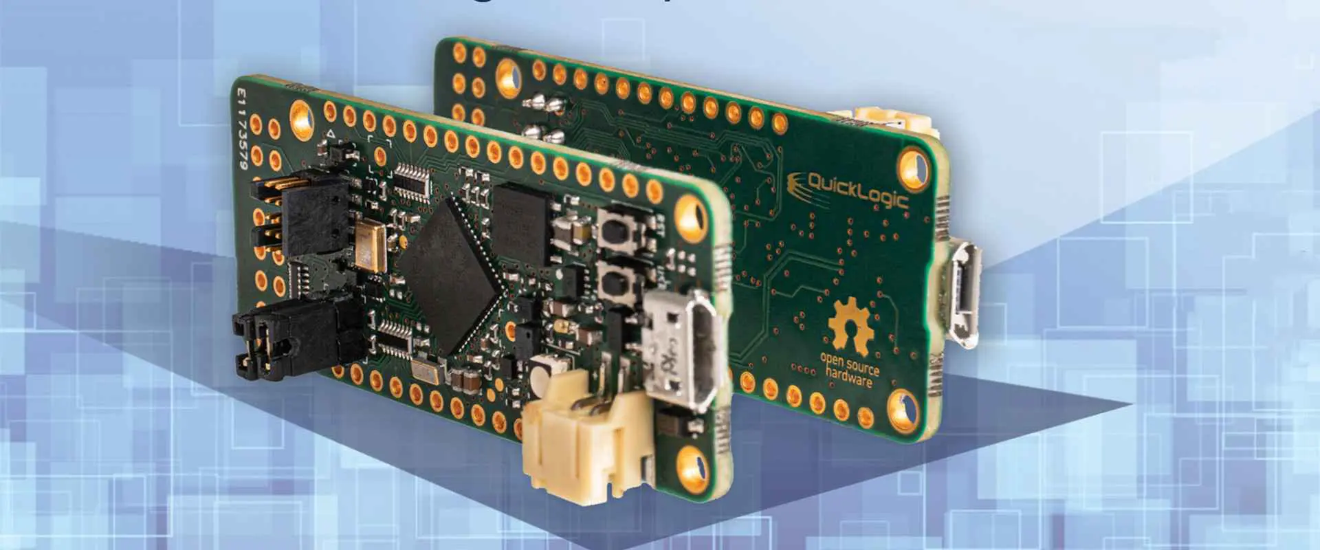
QuickLogic QuickRAM FPGA
The QuickLogic QuickRAM FPGA Family comprises Integrated Circuit (IC) devices. As a result, it provides low-cost, high-performance, easy-to-use embedded memory.
QuickLogic’s products depend on the popular LatticeMico32™FPC180. It is essential for embedded applications with the proven benefits of low power and advanced architectural features. In addition, it offers a solution for designs that require extreme speed, computing, and persistence.
The QuickRAM family of ESPs have up to 90,000 High Performance, Low-voltage CMOS SRAM bit cells. Each cell can store up to 4 bytes of data, which is eight times greater than Lattice’s MicoESP8X10 device. The higher density allows better performance and lowers cost. In addition, it contains a range of 160 to 1,584,000 bits of user-programmable non-volatile memory.
QuickLogic’s QuickRAM devices can operate on a wide range of voltages (1.8V, 3.3V, and 5V). However, because they operate on very low voltage, they don’t require power adapters and can also be helpful in battery applications. In addition, designers can cascade multiple RAM devices. Additionally, they connect them to external SRAM devices over low-voltage differential signaling interfaces.
These devices are fast enough to be helpful in many different applications. They are big enough to hold large amounts of non-volatile memory. They can be helpful as a part of a boot-loader program or as an application’s persistent storage.
Electrical Specifications
The QuickRAM family of devices is available in a range of packages/. They range from QFN-32 (14mm x 14mm) that can hold up to 2Mbits, to a QFN-100 (14mm x 14mm) that can hold up to 1Gb. They contain Vdd, Vss, and Vcc external pins and I/O, /RST, and TEST pins. Fast/Slow Mode bits select between Normal operating speed or High-Performance mode (2X) with the same clock frequency. The Power Dissipation is 3.2mW in normal mode and 21mW in High-Performance mode.
The QuickRAM family of devices is available with a wide range of data widths. The package footprint is small enough to allow deep board integration and dual-data-rated signal support. In addition, these devices contain up to 60MHz internal clock multiplier that allows the device to output twice the frequency of the input clock.
AC Characteristics:
The QuickRAM devices operate on a single supply of VDD, or 2.7V to 5.5VDC. This ensures compatibility with a wide range of designs. They may use voltage regulators and power supplies that don’t have a high tolerance to voltage levels.
The QuickRAM devices provide fixed voltage levels. However, VDD or VSS can drive the floating input and output pins. The floating pins should not remain floating for long periods because of potential noise and power consumption issues.
DC characteristics:
The QuickRAM devices are essential for maximum signal integrity with a deterministic rise and fall time of 50nS on all the outputs. The input signals can accept ≥ 2.0V in High-performance mode or ≥ 1,3V in Normal mode.
The device’s external input and output resistance are between 1kΩ and 10kΩ. This provides a low input capacitance with a fast rise/fall time. In addition, it ensures the dissipation levels remain to a minimum during transitions from 0 to VDD or VSS and vice versa.
The devices have a test pin that allows direct access to the device. This is available with 2.7V and 5.5V supplies and can read and write data directly from the non-volatile memory core. So, we can use it for self-test or on-chip debugging of the FPGA logic.
Power-Up Sequencing
The QuickRAM family of devices can accept power on their VDD or VSS pins. Therefore, we must power the unit up before sampling and verifying the output signals. We usually do this with a single-clock pulse in Normal mode and multiple clock pulses in High-Performance mode.
The QuickLogic QuickRAM ESPs can offer an industry-standard pinout. They also offer interface layout arrangements to design their products with ease. In addition, they feature standardized data, clock, and control pins for easy access to I/O functions. Also, they feature common interfaces such as power (VDD), data (Vss), clock (Vcc), and reset (I/O). As a result, we can easily cascade the QuickLogic QuickRAM ESPs to other devices, such as SRAM and FPGAs.
The QuickLogic QuickRAM Family provides an unusually large high-density bit cell of 4 bytes. However, this does not mean the bit cell size is equal to the number of 3-state read/write control output pins. Instead, the number of bits equals the number of 4-state reads/write control input pins.
This means that a 1Mbit device has a size similar to 8,000 8kbit devices.
JTAG
The QuickRAM devices contain a JTAG interface that can access the internal circuitry or perform on-chip programming. The JTAG interface is on pad one and consists of 3 test pins. Each input pin is accessible as a 4-state input pin.
JTAG tests allow users to reduce system complexity and potentially reduce development time by eliminating the need to add pull-up resistors or level converters to their system signals.
I2C
The QuickRAM devices also include I2C functionality to use the devices as simple non-volatile memory devices. The I2C interface is accessible on pad two and consists of 2 test pins that can be helpful as an input or output pin. Each input pin is accessible as a 4-state input pin. Therefore, we can configure it to access a single bit or multiple bits in the device.
Features
Advanced I/O Capabilities
The QuickLogic QuickRAM devices come in a wide range of packages, ranging from QFN-32 (14mm x 14mm) that can hold up to 2Mbits, to a QFN-100 (14mm x 14mm) that can hold up to 1Gb.
In addition, designers can cascade multiple RAM devices and connect them over low-voltage differential signaling (LVD) interfaces.
They provide fixed voltage levels. However, VDD or VSS can drive the floating input and output pins.
High-Performance Silicon
They can be helpful as a part of a boot-loader program or as an application’s persistent storage. These devices provide the designer with multiple options to ensure the best fit for their system design. It is available in various packages, including QFN28, QFN32, and QFN-64 which provides designers with optimal design space utilization for high-density applications. The QuickLogic QuickRAM I2C/SMBus-compatible device offers up to 1Gbits of bit cell density in 14mm x 14mm packages.
So, the QuickLogic QuickRAM I2C/SMBus-compatible device is available in QFN32, QFN64, BGA100, and BGA144 packages with 100MHz to 250MHz operation.
The QuickLogic QuickRAM I2C/SMBus-compatible devices are available in various density sizes from 64KB to 2Mbits.
Easy to Use/Fast Development Cycles
The QuickLogic QuickRAM devices are ready to use with all FPGA development tools and packages. In addition, their pinout and testability are compatible with most of today’s FPGA systems and programming tools.
Some applications developed using the QuickLogic QuickRAM devices are non-volatile memory, flash memory, SRAM, dual-port RAM, etc. Additionally, we can easily cascade it to other products.
The development cycle reduces significantly compared with other LSI package solutions. Therefore, designers can focus on their application instead of planning their bit cell layout.
High-Speed Embedded SRAM
The QuickLogic QuickRAM XC is a 2-level memory device used as programmable non-volatile memory to store application data. It is available in QFN-28, QFN-32, and QFN-64 packages, with 100MHz to 250MHz operation.
The QuickLogic QuickRAM XC is an 8Kbit SRAM device with 64KB of internal flash memory, allowing the user to program it up to 100ns. You can write the boot loader using the bank select pins (SMBus address) triggered by I2C or JTAG interfaces.
Eight Low-Skew Distributed Networks
The QuickLogic QuickRAM devices are carrier-grade High Speed embedded SRAM. Also, they can be helpful to connect to an FPGA system and provide the user with multiple options to ensure the best fit for their system design.
It makes it easier to integrate into an FPGA system and use it in a wide variety of technologies.
Up to 316 I/O Pins
Up to 316 high-performance, I/O pins can be available for designers to utilize in their FPGA designs.
The QuickLogic QuickRAM devices come in a wide range of packages, ranging from QFN-32 (14mm x 14mm) that can hold up to 2Mbits, to a QFN-100 (14mm x 14mm) that can hold up to 1Gb.
In addition, designers can cascade multiple RAM devices and connect them over low-voltage differential signaling (LVD) interfaces.
High Performance & High Density
These devices provide the designer with multiple options to ensure the best fit for their system design. It is available in various packages. They include QFN28, QFN32, and QFN-64, providing designers with optimal design space utilization for high-density applications.
The QuickLogic QuickRAM BGA100 and QuickLogic QuickRAM BGA144 devices are available in various density sizes from 64KB to 2Mbits.
Advantages of the QuickLogic QuickRAM FPGA
Easy to Use
The QuickLogic QuickRAM devices are ready to use with all FPGA development tools and packages. In addition, their pinout and testability are compatible with most of today’s FPGA systems and programming tools.
All signals come through a single 4-bit wide QFN package that reduces parasitics on all signals by removing unneeded inductors, capacitors, or resistors from the design. Thus, it boosts the performance and cost-effectiveness of designs.
Available in a Wide Range of Packages
The QuickLogic QuickRAM devices are available in various density sizes from 64KB to 2Mbits. Each input pin is accessible as a 4-state input pin and can access a single bit or multiple bits in the device. They provide fixed voltage levels. However, VDD or VSS can drive the floating input and output pins. The packaging choice considers the number of addresses and I/O available on the device itself.
Easy to Connect and Use
Three pins come on each side of the QFN package. We commonly connect these pins to FPGA memory and common digital or analog inputs and outputs.
Easy to Develop for
The QuickLogic QuickRAM devices have very fast access times. Therefore, it allows designers to run their applications faster than other solutions. In addition, the device is compatible with most FPGA development tools and packages.
Fast Design Cycle
The QuickLogic QuickRAM devices are ready to use with all FPGA development tools and packages. Their pinout and testability are compatible with most of today’s FPGA systems and programming tools. It takes approximately 2 minutes to program the QuickLogic QuickRAM XC SRAM device from a fully programmed EPROM device.
Wide Platform Support
The QuickLogic QuickRAM devices are compatible with a wide range of FPGAs and integrated circuits. They include Xilinx devices such as the XC4000, XC5000, XLP100, XLP200, XLP400, XL7000-XC devices, and the XC2XXX family.
Worldwide Support
The QuickLogic QuickRAM devices operate worldwide by an extensive after-sales service network. In addition, they use a global network of distributors, resellers, and trained engineers.
Accurate Timing
All parameters on the QFN package meet the required specifications while maximizing all benefits of the QFN process. The clock cycle speed is 2.5ns from 100MHz up to 250MHz.
Disadvantages of the QuickLogic QuickRAM
Data Security
To ensure data security, the QuickLogic QuickRAM devices come with various security options such as:
- A 32-bit signature register in each device provides a scrypt hash for the device’s contents. The signature register is programmable and not accessible by the user.
- A 64-bit counter holds the MAC address of the host or target device and can prevent illegal reprogramming of the device.
- The customer’s encryption or password can be set via the I2C interface. It prevents unauthorized access to QuickRAM silicon devices’ contents.
- Lockable 2-wire hardware serial interface data bus for further security measures
Power Consumption
The QuickLogic QuickRAM devices consume less power than other FPGA memory solutions and have a very low power standby current.
Environment Friendly
All QuickLogic QuickRAM devices are RoHS compliant and available in all packages. They include QFN-64 and QFN-100. It means that they can be helpful in today’s most advanced automotive, industrial, handheld medical devices and portable consumer electronic devices such as mobile phones and MP3 players.
Immersion and High-Temperature Applications
The QuickLogic QuickRAM devices are available in SOIC, TSSOP, and QFN packages to allow immersion applications. The QFN-64 allows usage up to +110°C, while the QFN-100 allows up to +150°C.
Quality and Reliability
QuickLogic QuickRAM devices have built a strong reputation for quality, reliability, and customer support. They have an extensive history of successful applications across various markets, including automotive, industrial and military.
Technical Attributes
The QuickLogic QuickRAM XC SRAM devices provide several technical attributes to assist designers with system design. These include:
Typical Operating Supply Voltage:
The device requires 3V or 5V of operating supply voltage for operation.
Supplier Package:
The MQFP-64 package is available from our supplier, and the QFP-100 package is available from our supplier.
Speed Grade:
The device can meet the JEDEC standard for SDRAM devices. This provides the device with the high performance and reliability required in automotive, industrial, and military applications.
Screening Level:
The device qualified to meet the AEC-Q100 Grade 3 standard. This provides the device with a high degree of integrity and reliability required in military and aerospace applications.
Re-programmability Support:
We can reprogram the device with new data, logic, and I/O functions using either an external programming source or an I2C interface.
RAM Bits:
We can program the device to store 64 or 128 bits in memory.
Product Dimensions:
The package size for the QFN-64 package is 25.4mm x 21.5mm, and for the QFN-100 package, it is 28.6mm x 18.2mm.
Pin Count:
The pin count is 208 for the QFN-64 package and the QFN-100 package. The number of I/O pins depends on the density used.
Operating Temperature:
The device has a maximum operating temperature of +70°C. The maximum operating temperature depends on the package selected.
Number of Registers:
There are 876 chip registers on the QFN-64 package and 38 on the QFN-100 package. Some of these are accessible to I/O pins, and some are accessible only internally to the device. The Detail Register Descriptions section gives a detailed description of each register.
MSL Level:
The device can meet theMIL-STD-461E Standard for Military Devices using QFN-64 and QFN-100 packages. These devices are essential for applications requiring safety factors to keep the device powered up during a normal operation over +70°C.
Mounting:
The device comes on a QFN-64 or QFN-100 package. It can be directly soldered onto a printed circuit board with a reflow oven and then encapsulated. The package provides blind and buried options as per the customers’ requirements.
Minimum Operating Supply Voltage:
The minimum operating supply voltage is 3V, and a low level of 0V can reset the logic cells. The device has a built-in watchdog timer that supports application software resets in the event of device lockups. The device can be automatically reset via an I2C interface, an external signal, or an external clock level to recover from system failures.
Maximum Propagation Delay Time:
The device logic cells have a propagation delay time of 1.4ns. Therefore, we can use the QFN-64 packages for 100MHz devices with a maximum clock frequency of 250MHz. On the other hand, the QFN-100 packages can be helpful for 250MHz devices with a maximum clock frequency of 500MHz.
Maximum Operating Supply Voltage:
The device has a +1.8 to +3V. The user can program the control register to select between 3V and 5V.
Maximum Number of User I/Os:
There are 320 I/O signals available on the QFN-64 package and 480 I/O signals available on the QFN-100 package. We can easily access each signal as an open drain, 4-state input, or output pin. In addition, the user can program a single logic cell or multiple logic cells to access single or multiple logic units. The total number of bits that we can access at one time depends on the density used.
Maximum Internal Frequency:
The device has a maximum internal frequency of 500MHz. However, the user can program the control register to select between 100MHz and 250MHz.
Lead Finish:
They fully finish the device through the entire process, from the first die to the last test. They print the QFN-64 package and pre-tin the QFN-100 package at all times.
Device Logic Units:
The device logic units can read 64 bits per clock cycle. The number of logic cells allocated to each logic unit is fixed and depends on the device’s density.
Device Logic Cells:
The device is partitioned into 64K logic cells, each accessed through a single clock cycle. We fix the allocation of logic cells to address I/O pins, and the customer cannot change.
Brief Description of the Device Structure
The QuickRAM device structure is a hierarchical VLIW logic structure. We partition it into three sections: a primary logic and address assist logic unit (AAU) and a secondary logic unit (SLU). You can access the primary logic, AAU, and SLU, through the I/O pins to form one part of the QuickRAM architecture. The internal address lines are helpful to form another part of this architecture. Finally, the external address lines are helpful to communicate the starting address of the primary logic from the AAU. The primary logic and AAU are on one side of the device, while the secondary logic is on another.
The SLU has three parts: a register memory, a data memory, and an enable memory. The register memory receives control signals from the primary logic. It provides internal registers that enable write access to the data memory and external I/Os in either the X- or Y-direction. In either direction, the data memory provides read access to internal registers and external I/Os. An external clock is essential for any device with a secondary logic unit.
QUICKLOGIC QL4009 Family
QL4009-3PFN100C, QL4009-3PL68C, QL4009-3PF100I, QL4009-3PF100C-5557, QL4009-3PF100C-5556, QL4009-3PF100C, QL4009-3PF100, QL4009-2PL68C, QL4009-2PF100C, QL4009-2PC68C, QL4009-1PL84C, QL4009-1PF100I, QL4009-1PF100C, QL4009-0PL84C, QL4009-0PL68C, QL4009-0PFN100C, QL4009-0PF100I, QL4009-0PF100C
QUICKLOGIC QL4016 Family
QL4016-0PF144C, QL4016-2PFN144I, QL4016-PF144, QL4016-PF100, QL4016-OESPL84C, QL4016-OC-5331, QL4016-4PF144I, QL4016-4PF100C, QL4016-3PF144I, QL4016-3PF100I, QL4016-3PF100C, QL4016-2PL84C, QL4016-2PF144C, QL4016-2PF100C, QL4016-2CF100M, QL4016-1PL84C, QL4016-1PF144I, QL4016-1PF144C, QL4016-1PF100C, QL4016-0PL84C, QL4016-0PF144I, QL4016-0PF100I, QL4016-0PF100C
QUICKLOGIC QL4036 Family
QL4036-T3PF144C, QL4036-QFP144C, QL4036-OESPQ208C, QL4036-OESPF144C, QL4036-IPF144C, QL4036-3PQ208C, QL4036-3PF144I, QL4036-2PQ208C, QL4036-2PF144M, QL4036-2PF144C, QL4036-2PB256C, QL4036-1PQ208M, QL4036-1PQ208I, QL4036-1PQ208C, QL4036-1PF144I, QL4036-1PF144C, QL4036-1PF144, QL4036-0PQ208C, QL4036-0PF144I, QL4036-0PF144C, QL4036-0ESPF144C
QUICKLOGIC QL4058 Family
QL40589-1PQ208C, QL4058-3PQ24C, QL4058-3PQ240C, QL4058-2PQ240C, QL4058-2PQ208C, QL4058-2PB456C, QL4058-1PQ240C, QL4058-1PQ208C, QL4058-0PQ208I
QUICKLOGIC QL4090 Family
QL4090-3PQ240C, QL4090-T3PQ208C, QL4090-T3PB456C, QL4090-LPQ240C, QL4090-4PQ240C, QL4090-3PQ208I, QL4090-3PQ208C, QL4090-3PB456I, QL4090-3PB456C, QL4090-2PQ240M, QL4090-2PQ240C, QL4090-2PQ208M, QL4090-2PQ208C, QL4090-2ESPQ208C, QL4090-1PQ240C, QL4090-1PQ208M, QL4090-1PQ208I, QL4090-1PB456C, QL4090-0PQ208M, QL4090-0PQ208I, QL4090-0PQ208C
QUICKLOGIC QL80FC Family
QL80FC-APQ208C
Application of the QuickRAM FPGA
QuickLogic QuickRAM devices can provide a high-performance SRAM solution. They can work in various general-purpose FPGA platforms. Below are some examples of use cases:
Converter Applications
A QuickLogic QuickRAM device can replace a slower part in applications such as digital oscilloscopes, logic analyzers, and RAM-based data acquisition systems.
Memory Controller or DMA Applications
A QFN-64 device can be helpful as the main memory controller for a system. However, the QFP-100 devices can benefit RAM module applications as per Rayming PCB & Assembly requirements.
Multiplexed Devices
We can implement multiplexed devices using QFN-64 devices to build up the multiplexed memory cells.
High Data Rate Applications
QFN-64 devices can be helpful in high data rate applications such as wireless radio communication and high-speed internet applications. In contrast, QFP-100 devices can be helpful in high data rate applications such as CDMA applications.
Low Power Applications
QFN-64 or QFP-100 devices can be helpful for low power consumption applications such as stereo audio systems and display monitors.
Conclusion
In conclusion, QuickRAM FPGA devices are an excellent solution to SRAM needs. They combine speed, data retention, and programming flexibility with meeting a wide variety of applications.
QuickLogic is a registered trademark of Semiconductor Systems Limited. QuickLogic solutions enable semiconductor designers to create the most advanced devices for embedded, digital signal processing and communications applications that require high-performance memories, DSPs, and microprocessors.