We live in an era where manufacturers use software to manufacture and assemble electronic devices. Now, unlike in the past, manufacturers have to make sure that they use the right:
Hardware and,
Software
Using these two components, commercial manufacturing of electronic devices becomes pretty easy. Due to this reason, many manufacturers are turning away from traditional PCB assembly methods and moving on to SMT. But what exactly does SMT software entail? And what does the SMT File Format do? If these questions puzzle you, do not worry because we shall answer them both in this article. In addition, we shall also cover more interesting topics; hence follow along to learn more.
SMT files contain CAD 3-dimensional models. These models are usually in the ASM (Auto Shape Manager) format. SMT files store structure and 3-dimensional information about a component in ASCII text format.
What’s more, you can transfer SMT files between different apps, for example:
During the transfer of SMT files across these applications, they do not lose model fidelity.
SMT Files – Extended
The ASM (Auto SHAPE Manager) came from the Autodesk ShaperManager. But what is the ShapeManager, you might wonder? Well, the shapeManager is a 3-dimensional geometry modeling Autodesk inventor component. The component is also found in many other apps and has been in use since the early 2000s.
The ASM format lets you maintain the CAD model’s integrity when transferring models between CAD applications. For instance, you can develop a prototype in the Autodesk inventor application export it as an SMT file. After that, you can then import the model into another app, say Moldflow, for further processing.
ASM has two different extensions and variations:
Autodesk shapeManager Binary ( also known as the .SMB file) – saves content in Binary form
Autodesk ShapeManager Text (also known as the .SMT file) – saves content in ASCII format
To open SMT files, you must first understand the software that utilizes this file extension. In most cases, many different applications utilize this file format. You can call them file associations.
Some of the most popular apps that utilize this file extension include:
QuickBooks
IconAuthor SmartObject
Apollo Database engine Memo File
You can also easily open up any SMT file using various Autodesk apps, for example:
To get that SMT file up and running in the Autodesk Moldflow adviser app, follow these simple steps:
Move on to the home tab and click it
Head on to the import panel
Import
Select “file of type” on the dropdown list
Select “All models.”
Navigate on to the SMT file, click open
And that is it, you have your SMT file up and running in Moldflow adviser.
If you are using Autodesk FeatureCAM, use the following procedure:
Select file then import
Select file
Click open
With these simple steps, you get your SMT file up and running in no time.
Because SMT files use ASCII text to save your content, that means that you can also open them up in text editors, for example:
Microsoft Notepad
Apple TextEdit
However, you should also note that opening SMT files using text editors is not the same as opening them using CAD applications. The display is entirely different.
The current electronic industry is highly utilizing SMT software to process electronic devices. Due to this, more companies are now working on new SMT software to up the competition. Because of this competition, we now have more efficient apps that we can utilize to work on our projects. Here are some of the most recent SMT applications in the market.
ASM Works
You can now integrate a smart factory into your electronics manufacturing process with ASM works. The core package of ASM works offers a comprehensive solution to manage the shopfloor in a connected factory. What’s more, this software comes with eight upgrade modules. These modules greatly improve factory areas and individual processes according to your specifications.
Advantages of this software to manufacturers include:
No interference worries
Great compatibility
No worries about data transfer in between lines
You can launch and administer this suite’s tools from a central location, making it pretty efficient.
V-ONE
Are you a fan of customization? If so, then you most probably will like the V-ONE software. The software is a pretty customizable platform that lets you make data-driven decisions. Using the V-ONE software, you can access and even monitor a personalized dashboard, wherever they are, using a smart device.
The V-ONE software also helps technicians and operators manage their:
Assigned tasks
Maintenance tasks.
The most recent V-ONE software version has an e-ticketing functionality that works on mobile phones and PCs. And yes, you can customize the e-tickets to suit your needs. In addition, your clients can also request certain templates to customize their e-tickets.
Do you like to take precautions before moving on to make a major step? Well, that is what this software is all about. The TestWay software is a test optimizer simulator that produces outputs that help you:
Estimate the test coverage
Eliminate any redundancies
Minimize escape rate
The software lets you import schematics in varying native formats. It also creates electrical views and digitizes schematics. You can utilize this features to analyze your board against testability rules, boundary rules, and design. After this analysis, you can possibly define custom rules using scripts. What’s more, the software highlights:
Design
Boundary scans
Testability violations
All this makes sure that the board is testable before moving on to build the first print circuit board.
The software lets you import up to twenty native CAD formats. It can also carry out accessibility analysis on any board, which helps in terms of probe placement for FPT and ICT.
Conclusion
Commercial electronics manufacturers look for a:
Fast,
Cost-friendly,
Flexible, and
An efficient method to produce electronic devices.
SMT provides all this and more, and hence it has become pretty popular. SMT utilizes software to manufacture electronic devices, which makes it pretty flexible. This software utilizes the SMT file format, which is pretty efficient in this case. As for the software, there exists more than one so do not feel tied up. You can explore to find the one that suits you. We hope this article has given you all the answers you were looking for in terms of SMT files and SMT software.
Flux plays a critical role during the PCB soldering process, facilitating bonding between component leads, pads, and solder. Traditional clean fluxes require removal after soldering to prevent corrosion, while modern no-clean formulations can eliminate post-solder cleaning. This provides efficiency advantages, but no-clean flux has limitations too. Understanding the key differences allows selecting the optimal flux type for a particular application.
This guide covers:
The composition, properties, and functions of clean and no-clean fluxes
How the chemistry and residues differ
Cleaning requirements and reliability considerations
Usage recommendations for each flux category
Proper handling, storage, and application methods
Gaining a deeper understanding of flux technology enables optimizing the soldering process for efficiency, quality, and reliability across the wide range of electronics assembly applications.
Flux Purpose and Function
Before comparing clean and no-clean fluxes, it helps to understand what flux does. The main purposes of flux during soldering are:
Removing Surface Oxides
Solder alloy and metal component surfaces form thin oxidized contamination layers. Flux chemically strips these oxides so solder can wet and adhere to the clean surfaces underneath.
Preventing Re-Oxidation
Once surface oxides are removed, flux provides a protective barrier preventing re-oxidation while the solder is molten during reflow or hand soldering.
Facilitating Wetting
Flux modifies surface tension properties to allow molten solder to spread out, cover, and wet the component and board surfaces thoroughly.
Residue Removal
Some flux residues must be cleaned after soldering to prevent harmful effects on the assembly. No-clean fluxes aim to not require cleaning.
Flux formulations utilize various chemistries, which dictate their properties and best usage. Common flux chemistry types include:
Rosin (RA) Flux
The most common traditional flux, composed of natural rosin extracted from pine sap. Lower activity and non-corrosive. Requires cleaning.
Organic Acid (OA) Flux
Synthetic carboxylic acids as the main activator. Moderate activity, suitable for soldering many metallic surfaces. Usually requires cleaning.
Inorganic Acid (IA) Flux
Contains strong mineral acids as activators. Highly active but much more corrosive. Typically requires cleaning.
Water-Soluble (WS) Flux
Blend of organic acids and amine hydrohalide activators. Moderate activity, but residues are water washable.
No-Clean (NC) Flux
Varied chemistries with mild organic activators. Low solids residue designed not to need cleaning after soldering.
There is some overlap between the properties of these categories, but this generalization highlights the key traits of each flux type.
Clean Flux Overview
Clean fluxes represent the traditional general-purpose option, encompassing rosin (RA), organic acid (OA) and inorganic acid (IA) formulations. Key characteristics include:
Medium to High Activity
Clean fluxes exhibit moderate to excellent soldering capability for surfaces with heavier oxidation or contamination. Rosin provides the gentlest clean flux, with increasing activity through OA and maximum activity from IA types.
Potentially Corrosive Residues
Flux activators are often acidic compounds that can damage board and component materials if residues remain. Even mildly activated rosin fluxes require removal.
Required Post-Solder Cleaning
The residues must be fully washed away after soldering using suitable solvents. Any remaining activators may continue attacking materials.
Readily Available
Clean fluxes have been used for decades in electronics assembly. Numerous suppliers offer a wide range of chemistries, gels, applicators, and supporting cleaning processes.
Clean fluxes provide strong soldering performance for difficult surfaces, but do necessitate process steps for post-solder residue removal.
No-Clean Flux Overview
No-clean fluxes were developed starting in the early 1990s to simplify assembly by eliminating the cleaning stage. Key attributes include:
Low Solids Content
No-clean formulations have just 1-5% flux residue content versus up to 35% for some paste fluxes. This reduces total residues.
Mild Activators
No-clean fluxes use relatively gentle organic activators that are minimally reactive after soldering when cooled. This reduces potential for damage.
Designed to Not Need Cleaning
If applied properly within limits, no-clean fluxes leave safe, benign residues that do not require removal after soldering.
Potential Reliability and Performance Tradeoffs
Reduced flux activity can increase defects. Residues may still cause issues in some environments over time.
No-clean flux provides production efficiencies but requires balancing tradeoffs in soldering quality, material compatibility, and long-term reliability.
Comparing Properties of Clean and No-Clean Fluxes
Clean and no-clean fluxes exhibit significant differences in their properties and performance which guide appropriate application:
Property
Clean Flux
No-Clean Flux
Activity Level
Medium-high
Low-medium
Residue Amount
High
Very low
Corrosivity
Often high
Low
Residue Cleaning
Required
Designed to not need cleaning
Reliability Risk
High
Low-medium
Efficiency
Low
High
Availability
High
Medium
Well-formulated no-clean fluxes can meet soldering, material compatibility, and reliability needs for many consumer, commercial, and industrial electronics assemblies while boosting efficiency.
No-clean residues are designed to be benign when left on assemblies. But some reliability risks remain which are examined next.
Reliability Considerations: Clean vs. No-Clean
Since no-clean fluxes do not get removed, their residues must not interfere with circuit function or degrade the assembly over time. Here are key reliability factors to weigh for clean versus no-clean:
Surface Insulation Resistance (SIR)
No-clean residues must not substantially lower electrical resistance allowing potential leakage currents. Clean fluxes provide higher SIR.
Electrochemical Migration Resistance
Ionic residues absorb moisture and can create dendritic growths that electrically short traces. No-clean fluxes inhibit migration but risks remain.
Corrosion Potential
Reactive residues may continue attacking component leads and board metalization over time, eventually compromising connections. Less risk with no-clean but still possible.
Interfacial Compatibility
Flux activators could affect interfaces between component encapsulants or conformal coatings. No-clean residues are designed to be compatible.
Cosmetic Appearance
No-clean leaves clear, shiny residues versus discolored residues from cleaned fluxes. Cosmetics are unimportant for hidden solder joints.
While designed to mitigate reliability risks, no-clean fluxes demand tightly controlled processes and have limitations regarding sustainability and service environments.
Cleaning Requirements: Clean vs. No-Clean
PCB Cleaning
The core difference between clean and no-clean fluxes is whether soldered assemblies require post-process cleaning:
Metric
Clean Flux
No-Clean Flux
Cleaning agent
Solvents, surfactants
Not needed
Typical process
Batch cleaning
Not applicable
Cleanliness validation
SIR testing
Visual inspection
Cleaning challenges
Solvent handling, waste
None
Efficiency impact
High, slows production
No added steps
Eliminating cleaning provides major time and efficiency benefits. But no-clean processes must be closely monitored to prevent issues.
Flux Application Methods
Applying the optimal amount of flux is critical for both clean and no-clean usage:
Application Methods
Brush
Dropper
Spray
Foam
Automatic dispensing
Controlled Parameters
Flux deposit weight and area coverage
Uniformity of application
Localized application options
Consistent Processes
Specify flux application in assembly documentation
Train operators on proper techniques
Regularly validate and document flux application
Controlling flux application improves soldering yield while minimizing residues. This benefits both cleaned and no-clean assemblies.
Process Recommendations: Clean Flux
Here are guidelines to follow when using clean fluxes requiring post-solder cleaning:
Select flux chemistry with appropriate activity level for the surfaces being soldered
Apply minimum flux needed for effective soldering
Use foam fluxes or controlled dispensing for tight process control
Clean flux off boards as soon as possible after soldering
Validate cleaning efficacy with SIR testing
Work with environmental regulations regarding cleaning solvents
Closely following flux manufacturer recommendations enables utilizing cleaning fluxes effectively while mitigating risks.
Process Recommendations: No-Clean Flux
To reliably use no-clean fluxes, these are key process considerations:
Match flux activity to needs of assembly materials and components
Minimize flux application to reduce residues
Maximize soldering heat and time above liquidus to fully volatize flux
After soldering, allow flux residues to cool undisturbed until solidified
Perform regular process monitoring, inspection, and SIR testing
Adjust no-clean process limits based on field reliability
No-clean fluxes require disciplined process control and validation to avoid hidden reliability risks from residues.
Flux Handling and Storage
Best practices for flux storage and handling maximize shelf life and avoid process issues:
Store flux in original containers away from heat, cold, and contaminants
For refrigerated flux, allow it to reach room temperature before use
Mix flux containers before use to re-disperse settled solids
Keep flux containers covered during breaks in use to avoid evaporation
Avoid contaminating fluxes with dust or metals
Never mix used applicators back into flux containers
Handle fluxes safely using proper PPE like gloves and eye protection
Safety-critical electronics where residues could not be tolerated
For specialized industrial, aerospace, automotive, and military applications, the risks of no-clean flux may outweigh the efficiency benefits. But no-clean has become the norm in high-volume consumer electronics where process controls can be implemented.
In summary, understanding clean versus no-clean flux properties allows selecting the optimal flux chemistry for each application’s performance, efficiency, and reliability requirements. Proper control of flux amount, soldering process, and cleaning or residue mitigation steps are also essential to unlock the benefits of each flux type.
Frequently Asked Questions
Here are some common questions about clean and no-clean fluxes:
Can no-clean flux residues be cleaned if needed?
It is difficult since no-clean fluxes are engineered to avoid dissolving in common cleaning solvents. Secondary cleaning processes may only partially remove no-clean residues. It is better to ensure residues are benign rather than try cleaning.
When would clean flux be used today?
For very high-reliability applications where no-clean chemistry limitations would risk product function – aerospace, military, medical, etc. Also in large solder bath processes where higher activity is needed.
Does no-clean flux leave visible residues?
Minimal visible residues if the soldering process is optimized. The residues are designed to become clear and practically invisible once solidified after soldering.
Can no-clean flux be used with water wash processes?
Yes, but the flux chemistry must be tailored to be water-soluble. General no-clean types are not readily washable with just water.
What is the shelf life of liquid fluxes?
Refrigerated shelf life is typically 1-2 years for most flux chemistries. For ambient storage, shelf life ranges from 3-9 months. Manufacturer guidelines should be followed.
Conclusion
Both clean and no-clean flux chemistries remain essential for electronics assembly. Understanding their composition, properties, reliability factors, and process recommendations allows engineers to select the optimal flux type for each application. With careful control of flux amount and the soldering process, high product quality and efficiency can be achieved.
One important factor PCB manufacturers consider when choosing PCB material is environmental safety. Toxic substances do have a negative impact on the environment. Thus, it is important to avoid the use of toxic substances during PCB manufacturing.
Also, the Shengyi 1151G is a halogen-free PCB base material. This laminate is highly preferred among PCB manufacturers since it is environmentally friendly. In this article, we will reveal more information about the Shengyi S1151G.
What is Shengyi S1151G?
Shengyi S1151G is a lead-free compatible FR4 laminate. Also, this board is free of halogen constituents. Hence, it is safe for use. Shengyi S1151G serves as the base material for printed circuit boards. Also, this material features great thermal and mechanical properties. It is widely used for the production of single sided and multilayer boards.
Also, this board is ideal for use in applications demanding great thermal performance. Shengyi S1151G PCB material doesn’t contain any hazardous residue. In addition, this high CTI PCB material adheres to the standards of PCB fabrication. Also, Shengyi S1151G is free of toxic substances like red phosphorus and antimony.
Shengyi S1151G PCB material is lead free compatible. Therefore, this PCB features no lead materials. Also, it complies with the RoHS standards.
Environmentally friendly
Shengyi S1151G is safe for the environment. This PCB material is free of halogen. Halogen is a toxic substance with negative effects on the environment. Also, the Shengyi S1151G PCB base material is free of other constituents like red phosphorus.
High CTI
The comparative tracking index (CTI) of this PCB material is very high. Shengyi S1151G has a CTI ≥ 600. CTI measures how the insulating material of the circuit board can withstand unintended current to transmit between traces on the PCB. In addition, it measures how the substrate can resist breakdown between tracks on the PCB surface. The CTI helps to evaluate the resistance of the PCB material against environmental impacts like moisture.
UV blocking
This is another great feature of Shengyi S1151G. Also, this PCB material can block the impact of UV rays on the PCB.
Shengyi S1151G features great thermal, mechanical, and dielectric properties. These properties are peculiar to Shengyi S1151G.
Glass transition temperature
The glass transition temperature of Shengyi S1151G is 155 degrees Celsius. This value is high. The Tg value describes the temperature at which Shengyi S1151G changes from a solid state to a rubber-like state. Therefore, when Shengyi S1151G’s Tg goes above 155, there is a high risk of fire.
Decomposition temperature (Td)
The Td of Shengyi S1151G is 380 degrees Celsius at 5% weight loss. The decomposition temperature of a PCB material decomposes chemically. The decomposition temperature is very crucial when fabricating a circuit board. Shengyi decomposition temperature is above 320 degrees Celsius. Therefore, Shengyi S1151G has a great decomposition temperature.
Coefficient of thermal expansion (CTE)
The CTE of Shengyi S1151G is 220 ppm/℃ before glass transition temperature. The CTE of a PCB material measures how its size changes in relation to temperature variations. If the temperature of a material rises beyond its Tg, the CTE will also increase. Shengyi S1151G features a great coefficient of thermal expansion.
Dissipation factor
The dissipation factor of a material specifies the ability of a material to act as an insulating material. Shengyi S1151G PCB material has a dissipation factor of 0.011 at 1GHz. This value is considered low. Also, a low dissipation factor indicates low power loss.
Peel strength
The peel strength measures the ability of dielectrics and copper layers to remain together under chemical and thermal stress. Therefore, it measures the bond strength of dielectric and copper layers during stress. Shengyi S1151G’s peel strength is 1.4 N/mm at 288 degrees Celsius after thermal stress.
Low water absorption rate
Shengyi S1151G laminate features a low absorption rate of 0.10%. Therefore, this laminate can withstand humid environments.
Shengyi S1151G is AOI compatible. This is one great benefit of this PCB material.
Highly durable
Shengyi S1151G is very durable. This PCB material can resist varying environmental conditions. Also, it can function well in moisture conditions.
Free from toxic substances
This PCB material is completely free of toxic substances like halogen. Therefore, it is a recommended material for PCB fabrication.
How to Apply Shengyi S1151G on the PCB
PCB manufacturers use lamination machines to apply shengyi S1151G on circuit boards. Here is a step by step procedure of laminating multilayer boards.
Prepare your materials
This is very important for the lamination process. You need a multilayer PCB, lamination machines, and your Shengyi laminate.
Place the laminate
Place the layers of the PCB and ensure the laminate is in between. This means that you will bond the S1151G laminate between the PCB layers.
Laminate the board
Here, you will place the multilayer PCB in the lamination machine. Also, to boost the bonding process, the machine must be at high pressure and temperatures. After this, allow the material to get dry under high temperatures.
Shengyi S1151G is widely used in the automotive industry. This PCB material is used for designing parts of automobiles. Also, this material features great thermal and mechanical properties. Therefore, it is ideal for this application. This PCB material improves the performance of automobile features.
You will find Shengyi S1151G laminate in consumer electronics like television and refrigerators. Also, this PCB laminate is ideal for use in this application since it is halogen-free. The consumer electronics industry makes use of halogen free materials. Therefore, shengyi S1151G is a safe PCB material for the construction of consumer electronics.
Smartphone
Shengyi S1151G is commonly used in the production of smartphones. Smartphones feature PCB. However, it is safe to use a toxic-free PCB material for the production of these devices.
Conclusion
This article discussed Shengyi S1151G PCB material and its properties. Also, it discussed its benefits and applications.
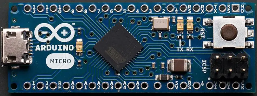
Arduino is an open-source electronics platform that uses easy-to-program microcontroller boards and software. The Arduino Nano and Arduino Micro are two popular small-form-factor boards in the Arduino family. They provide compact, breadboard-friendly options for Arduino projects.
But what exactly are the differences between the Nano and Micro? This guide examines the key distinctions in their specifications, design, hardware, and performance to help you select the right board for your needs.
Arduino Nano Overview
The Arduino Nano is one of the smallest classic Arduino boards, but still includes the essential components needed for many projects. Here are some key features:
Microcontroller: ATmega328P
Operating Voltage: 5V
Digital I/O Pins: 22
Analog Input Pins: 8
Flash Memory: 32 KB
Clock Speed: 16 MHz
Physical Size: 18 x 45 mm
Mounting Holes: No
The Nano’s small size makes it well suited for breadboard use and space-constrained projects. Its pin layout mirrors a standard Arduino Uno for easy migration between the boards. Overall, the Nano offers a versatile, economic option for many entry-level and intermediate Arduino applications.
The Arduino Micro is even smaller than the Nano but contains more powerful processor and networking capabilities. Key features include:
Microcontroller: ATmega32U4
Operating Voltage: 5V
Digital I/O Pins: 20
Analog Input Pins: 12
Flash Memory: 32 KB
Clock Speed: 16 MHz
Physical Size: 18 x 33 mm
Mounting Holes: Yes
The Micro runs on the more advanced 32U4 processor, adding built-in USB communication support. Its compact stamped form factor consumes minimal space. These advantages make the Micro a good choice for projects involving USB connectivity or advanced processing in a tiny package.
Hardware Comparison
While the Nano and Micro share similarities in being small Arduino boards, they differ significantly in their hardware design and component integration.
Processor/Microcontroller
Nano: ATmega328P – Common 8-bit AVR MCU, basic Arduino controller
Micro: ATmega32U4 – Enhanced 8-bit AVR with built-in USB support
The 32U4 gives the Micro native USB communication capability lacking on the 328P Nano.
Input/Output Pins
Nano Digital I/O: 22 pins
Nano Analog In: 8 pins
Nano PWM channels: 6
Micro Digital I/O: 20 pins
Micro Analog In: 12 pins
Micro PWM channels: 7
The Micro has 12 analog inputs versus 8 on the Nano, useful for more complex analog sensor applications.
Memory and Clock Speed
Nano Flash Memory: 32 KB
Nano SRAM: 2 KB
Nano EEPROM: 1 KB
Nano Clock Speed: 16 MHz
Micro Flash Memory: 32 KB
Micro SRAM: 2.5 KB
Micro EEPROM: 1 KB
Micro Clock Speed: 16 MHz
The memory configurations are nearly identical, with the Micro having slightly more SRAM. Both operate at 16 MHz.
Power
Nano Input Voltage: 5-12V recommended, 7-12V required for some functions
The Nano and Micro also use different processor families that impact compatibility with Arduino software libraries and cores.
Processor Family
Nano: ATmega328P (AVR 8-bit MCU)
Micro: ATmega32U4 (AVR 8-bit MCU)
Both are Atmel AVR chips but they require different cores to provide USB support on the Micro versus UART on the Nano.
Arduino Cores
Nano: ATmega328P core
Micro: Leonardo core
The Leonardo core adds USB communication libraries. Most shields and libraries are compatible with both cores.
Pin Mapping
Nano: ATmega328P Arduino pinout
Micro: ATmega32U4 Arduino pinout
Code written for Nano will need pin number changes to run on Micro. The pin functions match between boards but not pin locations.
Memory Management
Nano: Standard Arduino memory management
Micro: Enhanced memory management in Leonardo core
The Micro can more efficiently utilize its SRAM memory space than the Nano with the 328P core.
Performance Comparison
The Nano and Micro overall have generally comparable performance, but the Micro’s 32U4 architecture and USB support provide some advantages for specific use cases.
Processing Speed
Nano and Micro: Both 16 MHz clock speed
The two boards operate at the same 16 MHz frequency and thus equivalent raw processing rates.
Input/Output Speed
Nano: Standard I/O performance
Micro: Slightly faster I/O operation for analog and PWM functions
The 32U4 MCU implements some peripheral functions like ADC and timers in a more optimized fashion.
Interface Speed
Nano: UART capped at 2 Mbps
Micro: Hi-speed USB 2.0 with transfer rates up to 480 Mbps
The Micro’s integrated USB connectivity provides vastly faster throughput than the UART interface on the Nano.
Responsiveness
Nano: Some delays managing USB-serial coordination
Micro: Native USB operation avoids UART delays
USB HID allows lower latency control of the Micro from a host computer compared to Nano’s conversion between USB and serial.
Program Storage
Nano: 32 KB flash for storing sketches
Micro: 32 KB flash for storing sketches
Both provide the same size 32 KB flash memory for storing Arduino sketches.
Cost Comparison
The Nano and Micro have similar manufacturing costs in the same low price range:
Arduino Nano pricing: Approximately $22 – $25
Arduino Micro pricing: Approximately $20 – $25
For either board, 3rd party clones can be purchased often for $10 or less.
In summary, the cost is essentially equivalent between both models when sourcing original Arduino or clone boards. Cost does not need to be a determining factor.
Usage Comparison
The Nano and Micro lend themselves to somewhat different use cases based on their size, design, and hardware differences:
Arduino Nano Typical Uses:
Basic microcontroller learning and experimentation
Physical computing projects with simple interfacing
Low-speed human interface devices like game controllers
For projects with these basic embedded control needs, either Nano or Micro could suffice. The smaller form factor Micro may work better in tightly constrained spaces.
In summary, the Arduino Nano and Micro share similarities in their compact format and basic microcontroller capabilities. But key differences exist in their I/O configuration, physical design, and especially USB support that impact their use in various applications:
The Nano provides a compact, no-frills option for basic Arduino projects not requiring USB. Its rectangular PCB shape and standard pin layout offer versatility.
The Micro is best for advanced projects needing USB native connectivity to PC or other devices. Its tiny, stamped footprint can fit into the smallest spaces.
For projects that simply need a small Arduino board without USB or specificity on form factor, the lower cost Nano is likely the better choice. But for space-constrained applications requiring direct USB integration, the Micro’s advantages stand out. Understanding these tradeoffs allows selecting the right board for each project’s needs.
Frequently Asked Questions
Here are some common questions about the Arduino Nano and Micro:
Can shields be used with the Nano and Micro boards?
Yes, both Nano and Micro are compatible with standard Arduino Uno shields since they have the same operating voltage and I/O pin capabilities. However, the smaller physical size may block some shield attachments in compact layouts.
How difficult is transitioning code between the Nano and Micro?
The code can usually be adapted quite easily by changing pin numbers to match the different layouts. But sketches relying on UART serial functions will require changes to use the Micro’s USB capabilities instead.
How do you connect the Nano and Micro to a computer?
The Nano requires a separate USB-to-UART adapter, while the Micro provides built-in USB connectivity. Nano thus needs extra wiring and components to interface with USB.
Can the Nano or Micro be battery powered?
Yes, both boards can run on batteries or other standalone power supplies from 5-12V. Avoid exceeding 12V maximum input voltage to prevent damage. The Micro’s size can be advantageous for portable, battery-operated devices.
Which board is more beginner friendly?
For complete beginners, the Nano is likely easier to start with since its functionality matches the familiar Uno. After gaining experience, the Micro’s extra features become more useful. The Micro may seem more complex at first.
Conclusion
The Arduino Nano and Micro each have specialized strengths for different applications. Understanding their key hardware and software differences allows selecting the right board to best meet the needs of a particular microcontroller project. For basic low-cost Arduino projects, the Nano provides a compact solution. Where advanced processing and USB connectivity are required, the Micro is likely the superior choice.
Among the many cyanate ester epoxy laminate and pre-preg materials, we consider Nelco N8000 series as one of the high-Tg materials. As a result, this material is ideal in board designs that require finer lines, higher layer counts, and larger panel sizes. It also features excellent thermal management characteristics.
It delivers exceptional laminating performance and product integrity. In addition, its flame-resistance properties make it a superior choice for various applications.
The Rogers SpeedWave 300P ultra-low-loss resin system is a high-performance, low-dielectric-coefficient pre-preg. It bonds a wide range of Rogers laminates, including CLTE-MW, RO1200, and RO4000. These high-quality, repeatable electrical properties make them ideal for various applications.
Nelco N8000 Cyanate Esteer Epoxy Laminate and Prepreg are cyanate ester laminates with high-Tg that provide outstanding thermal and mechanical properties. This laminate material is the best for board designs that may require higher layer counts and finer lines. Its dimensional stability allows it to fit into huge panel sizes. This product line offers an extensive range of high-quality pre-preg options for various electronic boards.
RF PCB board is a high-performance cyanate ester epoxy laminate. Its thermal and halogen-free properties make it ideal for automotive radar sensors, 5G wireless communication, and satellites. In addition, its low dielectric-tension properties make it a highly versatile material. Its versatility allows for a wide range of uses.
CYCOM EP2750 is an enhanced epoxy resin system that allows high-speed aerospace structural parts manufacturing. The CYCOM EP2750 is an acetal acid-based epoxy. Its thermal and electrical properties are exemplary for aerospace applications, including RF printed circuit boards. Additionally, the CYCOM EP2750 is also an excellent choice for high-rate PCB fabrication.
The N4000-13 SI is ideal for RF and microwave copper clad laminates. As a result, this material is the preferred choice for many transceiver-based applications. RF/microwave materials are compatible with a wide range of frequencies. For example, it has a low dissipation factor and is suitable for assemblies with a maximum reflow temperature of 245 degrees Celsius.
The Nelco N8000 Cyanate Estere Epoxy Laminate and Prepreg are highly durable and have a high Tg. Its Tg allows for reflowing and assembly cycles and offers a low-loss solution for electronic circuits. Typical-thickness laminates are available in either pre-preg or bondply forms.
A cyanate ester epoxy laminate and pre-preg material derived from the chemical cyanate. These materials are often helpful in the production of printed circuit boards. The advantages of these laminates include low-pressure lamination, which prevents microcracks. In addition, unlike traditional FR-4 processes, cyanate esters can be processed using standard FR-4 methods.
Exceptional reflow properties
The N4000-13 SI is a two mil system with exceptional reflow properties. Its superior signal integrity ensures high reliability and precise impedance regulation. This cyanate ester laminate is suitable for assemblies with a maximum reflow temperature of 245°C. The N4000 series also offers excellent signal loss properties, a broad bandwidth, and low CTE on the Z-axis.
A variety of features are available in this epoxy laminate and pre-preg, including low glass transition temperature and an e-glass alternative. The N4000 series is a specialized product for multilayer printed circuit boards and high-speed digital applications. Its advanced epoxy resin system offers excellent thermal management features and low signal loss. So, it is also available in a two mil system.
The N8000 series of cyanate ester epoxy laminate and pre-preg is a highly versatile, flexible cyanate-ester epoxy material that exhibits exceptional flexural and mechanical properties. In addition, its glass transition temperature is lower than its competitors and exhibits a higher reflow temperature than the former.
Resistant to high temperatures
In addition to the Tg and PTR, the N8000 Cyanate Ester Epoxy laminate and pre-preg are resistant to high temperatures and low pressure. It is an ideal substrate for various printed circuit boards and offers superior strength and rigidity. The PTC board is an asset for Rayming PCB & Assembly. Additionally, its high flexural strength, it is also compatible with a wide range of other electronic products.
The N8000 Cyanate Ester Epoxy laminate and pre-preg offer high reliability and a variety of constructions. The N8000 is compatible with various temperature ranges and can handle extremely high reflow temperatures. The high reflow temperature of the N8000 makes it an ideal choice for many applications. In addition, the low reflow temperature ensures that it will stand the test of time.
The N8000 Cyanate Ester Epoxy and Prepreg are ideal for high-frequency applications. This type of laminate is ideal for applications where high-speed data transmission is required. So, it is also ideal for multilayer PCB. These PCBs are available in various materials, including polyimide, FR-4, and PTFE.
Cyanate ester resins are not new to the industry, but their applications were previously limited. The cyanate ester process is the most effective in eliminating microcracks and improving electrical properties. We typically process this material through standard FR-4 processes. It is often helpful in the construction of multilayer printed circuit boards. The process also provides superior mechanical and thermal properties.
The low-pressure cyanate ester lamination process limits the amount of energy stored in the laminate, released during thermal cycling, and exposed to caustics. The energy released is responsible for various failures in the composite. The high-pressure cyanate ester lamination procedure results in a low Tg. The re-curing temperature should be 260 degrees Celsius or 240 degrees Celsius. The stackup design should ensure the composite’s signal integrity and power performance.
This process has low-pressure cyanate ester lamination. Because of its low-pressure nature, the laminate limits the amount of energy stored in the composite. Therefore, we release this energy during the curing process and caustics. This release of energy can lead to various failure mechanisms in multilayer cyanate ester printed circuit boards.
Conclusion
Nelco N8000 is a high-Tg, cyanate ester epoxy laminate and pre-preg material ideal for high-layer-count and fine-line board designs. The material also has superior mechanical and electrical properties, making it an excellent choice for large-panel designs. This guide will discuss the pros and cons of using this high-tech material.
The N4000-13 SI is a high-performance PCB substrate that provides excellent impedance regulation and optimum signal integrity for high reliability. This water-based material is suitable for reflow temperatures up to 245 degrees Celsius and can be processed as high as 260 degrees C. In addition, it has excellent signal loss properties and a low Z-axis CTE, which makes it an excellent choice for applications in the 1-10 GHz frequency range.
The N8000 Cyanate Ester Epoxy Matrix has excellent thermal and electrical properties. It is suitable for a wide range of applications and has a high-temperature range. As a result, it has a low Z-axis CTE. In addition, it has a low signal dissipation factor, ideal for high-frequency audio and video products.
It is essential to consider the application of a Nelco PCB. The N4000-13 SI is suitable for high reliability and precise impedance regulation applications. Therefore, it is ideal for high-temperature reflow temperatures. However, high thermal expansion rates result in a fast vertical expansion, over-pressing via structures. This can cause fractures.
Solder is an important element commonly used in the electronic industry. The uses of solder can’t be overemphasized as this element plays vital roles in the production of electronic devices. However, this element has its own melting point. This article seeks to shed more light on the melting point of solder.
What is Solder?
Solder is a metal alloy that comprises tin and lead. Solders help to join two or more components together. This metal alloy consists of several alloy compositions with melting points as high as 400°C. Also, the melting points could be as low as 90 degree Celsius. Solder helps to create huge bonds of permanent nature like copper joints in PCBs.
Temperature determines the melting point of any material. The temperature here refers to the temperature at which solid changes to liquid. Also, this temperature specifies the type of materials to use in a real world application. Solders melt and bound electrical components. The melting point of solder determines the choice of solder alloy for an application.
For instance, if the device will function under high temperature, the solder must have a higher melting point than the operating temperature. This means that the operational environment of a device determines the melting point of solder.
The right melting point of solder is about 250 degree Celsius. This specifies a good quality solder metal. Also, you can determine the quality of a solder through its high conductivity and low flux content. Solder comprises an alloy of lead and tin. This tin can be 60% while the lead is 40%. Also, this solder has a varying melting temperature range. However, it will start melting at 361.4 °F. Also, it will turn to a full liquid at 375.8 degrees Fahrenheit.
A solder with 50% of tin and 50% of lead has a melting range between 361 °F and 421 °F. The melting point of a silver solder is 1145 °F. This solder melts until it gets to 1145 °F. Also, Zinc/aluminum solder has high melting point of 719.6 °F. A 70/30 lead-tin grade solder features a melting temperature of 255°C. Therefore, the melting point of solder depends on its composition and type.
Categories of Solder
Another factor that determines the melting point of solder is its formulation. Solders can be Eutectic and non-eutectic.
Eutectic solder
This solder can easily melt. Therefore, eutectic solder describes a metal alloy that melts at a single temperature. Also, after cooling, this solder solidifies at a single temperature. Furthermore, some manufacturing processes require this capability.
Non-eutectic solder
This metal alloy can’t melt at a single temperature. Also, this type of solder has a melting range. Eutectic solder starts melting at a particular temperature. Then it continues melting as the temperature rises. Also, the melting stops when the solder reaches the final temperature and the alloy is liquid.
The melting range is the difference between the melting finish and the melting start temperatures. Some solders’ melting range is 75 degree Celsius. The melting range can be as low as 32 degree Celsius.
The choice of a solder alloy depends on several factors. However, the two major factors are:
Subsequent thermal processes
Solder melting point of the process
A manufacturer may demand a high temperature solder since there will be subsequent thermal processes. Also, the high temperature solder gives him the freedom to carry out more than one thermal process. However, a low temperature solder might be necessary when the components involved are thermally sensitive. These components can damage when exposed to high temperatures.
Types of Soldering
Soldering is a process that involves connecting different types of metals by melting solder. During soldering, two or more components are joined together. To achieve soldering, engineers melt the solder by using heat generated by iron. There are different types of soldering which include:
Hard soldering
In this soldering process, the engineer uses brass or silver. Also, this type of soldering creates a strong connection. To maintain a strong connection, this soldering demands a blowtorch. This helps to increase temperature and melts the base metal.
Soft soldering
Soft soldering features the lowest filler metal melting point. Also, this soldering type utilizes low temperatures. However, it isn’t ideal for mechanical load-bearing applications. This is because it isn’t ideal for use in extremely high temperatures. Therefore, it is widely used in plumbing and electronics.
Soft soldering connects electronic components in PCBs. The lower temperature established a strong joint.
Brazing
This is the third type of soldering that uses metal with a higher melting point. The melting point of this soldering is higher than soft and hard soldering. Also, the bonded metal is heated opposite to the melted down metal. Brazing requires to sufficiently heat the material to achieve the best result.
Soldering is of great importance in several applications. The application determines the composition of solder. Below are the uses of soldering:
Electronic components
Soldering is widely used in electronic devices. It helps to create electrical flow. Also, soldering guarantees you electrical flow in residential or commercial wiring. Therefore, it is useful in merging wires to terminals in an electrical device.
Plumbing
Solders are of great importance when it comes to plumbing. You can use solder to join copper plumbing pipes. The lead-free solder is ideal for this application.
Auto repair
In this application, solder tightens the joints. Also, it smoothens the surfaces of auto parts. Although solder can’t fix engines, it can fill irregular cavities and tighten joints.
Printed circuit boards
In printed circuit boards, solders help to connect electrical components. Soft soldering helps to attach small components on PCBs. It helps to fix the component leads with the copper tracks. This ensures they are electrically connected.
Solder comprises three major materials which are flux, tin, and lead. However, there are several diversifications of solder based on the relative ratio of these materials. Furthermore, there are some additives and metals that you can add to solder. This helps to strengthen the conductivity of solder.
Copper enhances the wetting characteristics of solder. Also, it minimizes the melting point in any molten condition.
Antimony increases the mechanical strength of solder.
Nickel prevents the Under Bump Metalization layer (UMB) from any dissolution.
Silver provides great mechanical strength. However, it provides lower ductility than lead.
Conclusion
Solders are in several forms and shapes. The melting point of a solder determines a lot. The solder melting characteristics are a critical factor while selecting a solder alloy. However, there are other factors that determine the selection of the alloy.
When it comes to high quality laminates, the Shengyi Synamic8G PCB material is one that serves multiple functions. This is a type of laminate which you can use for various applications and multilayer circuit boards. With its water absorption rate, it is low and as such, it doesn’t allow water entry into the board.
Here, we will explain more elaborately all you should know about this laminate. Also, there are features that set it apart from other laminates and it is highly durable. Let us dive into the world of Shengyi Synamic8G PCB material.
What is Shengyi Synamic8G PCB Material?
This is a type of laminate whose lifespan is strong. That said, this means that it is a type of laminate that is long lasting and can bond layers together without any negative effects. There are some laminates that don’t hold up layers strongly. As a result of that, the layers begin to become weak and they loosen up.
Furthermore, the Shengyi Synamic8G PCB material offers a distinct performance with its excellent PTH reliability. This laminate is mostly used for multilayer circuit boards. Also, it is safer and better to hold multiple layers than other laminates.
In addition, this kind of laminate has exceptional thermal reliability which is one advantage to it. Therefore, this PCB laminate has thermal resistance. As we discuss more about the Shengyi Synamic8G, we shall focus on its features.
Which Application Can You Use Shengyi Synamic8G PCB Material For?
Accordingly, you can use this laminate for various applications. It is present in many modern day gadgets and automobiles. Well, it is used because it has the propensity to hold multiple layers in these applications.
Power Supply and Industrial
The Shengyi Synamic8G is present in many industries not limited to automobiles. This laminate helps to connect elements that transmit electrical power in linear or switched supplies. It helps bond layers with thermosetting resins. In this industry, it is used for electrical transformers.
Computer Electronics
The Shengyi Synamic8G is used for modern day computers. It is always present in the PCB board of the computers. Note that, for insulation in computers, this laminate is applicable.
Also, it helps to improve the general performance of computers. Thus, it connects the PCB and different layers together. It helps the computer expose to varying degrees of temperature without having any harmful effect on it.
Automation
Today, the Shengyi Synamic8G PCB is used in the automotive industry. Also, for many vehicles becoming computerized, this kind of laminate is for bonding the multiple layers in the circuit board. Certainly, it enhances the overall performance of any kind of automations.
Electronics
Every day, there is a production of more electronic appliances. One thing that makes it possible to connect the circuit board is this type of laminate. Also, the Shengyi Synamic8G is applicable in tools we use in our homes. You find this laminate in televisions, telephones, laptops, radios, and alarm clocks.
Optical Communication Services
The Shengyi Synamic8G PCB laminate is applicable in some cable protection systems. Thus, it is available in optical communication services like fiber optics, signal for mobile phones, ISDN, communication satellites, and POTS. The laminate helps networking in local areas quite possible.
High Frequency Equipment
This Shengyi Synamic8G PCB laminate is applicable in high frequency tools useful for measurement. Typically, it makes the frequency work effectively. Also, you find it in electromagnetic instruments for measurement, voltage instruments for measurement, and devices for measuring current.
What are The Features of the Shengyi Synamic8G PCB Material?
Just like other laminates, this type of laminate has peculiar features the same way it has its unique functions. Although some of these features are present in other types of laminates. However, there are considerable levels of degrees to which they function.
Exceptional anti-CAF Performance
The Shengyi Synamic8G PCB material has an excellent anti- Conductive Anodic Filament performance. Also, this laminate doesn’t allow any conductive salt which consists of copper form in the circuit board. The laminate ensures that the circuit board is reliable for use. Therefore, it enhances the performance of the anti-CAF. Thus, it has resistance to electrochemical abrasion.
Exceptional Thermal Reliability
When it comes to performance under high temperature, the Shengyi Synamic8G PCB makes it possible for applications to work. Meanwhile, this is as a result of the exceptional thermal reliability of this kind of laminate. One doesn’t have to worry any longer about high temperatures.
Also, the Shengyi Synamic8G has the potential to resist any high temperature and applications can work perfectly. Still, it is durable despite exposure to high temperatures.
Low CTE
One of the features of this laminate is the lower Z Axis CTE. This may be a feature of other laminates. However, the Shengyi Synamic8G has it in varying levels. This means, the coefficient thermal expansion is lower than some laminates.
Therefore, with any increasing temperature, this laminate expansion is never much. An increase in temperature doesn’t have much effect on how this laminate works in the circuit board. Also, there is stability in the way this laminate works despite exposure to high temperature.
High-TG Laminate
This is a type of laminate with high glass transition temperature. It requires a high temperature and as such can resist any temperature. It has high temperature durability as well as high glass transition temperature.
Highly Durable
This is a kind of laminate that lasts long. It is weather resistant and harsh weather cannot damage it. Also, the Shengyi Synamic8G ability to maintain stability and its CAF resistance nature makes it durable.
Yes, the Shengyi Synamic8G PCB is waterproof. The same way, it is weather resistant. It has low water absorption which means no water passes through it. The ability to retain its stability and work effectively is tied to its waterproof barrier.
Conclusion
The Shengyi Synamic8G PCB material is a very durable laminate that can bond layers together without loosening up. Furthermore, it has many features which makes it offer PTH dependency.
Also, this laminate is waterproof and is weather resistant. It uses various copper densities and is simple to make. This is a laminate that is useful in servers, routers, and switches.
Have you been searching for some reliable information about the Shengyi S1000-2M PCB material? You are in the right place.
In this article, we are going to discuss the features, properties, applications, etc of the Shengyi S1000-2M PCB material. Furthermore, we will be drawing some comparisons between the Shengyi S1000-2 and the Shengyi S1000-2M PCB material.
If you wish to be a pro in this area, why not join us as we take you through the important things you should know concerning the Shengyi S1000-2M PCB material.
Features of the Shengyi S1000-2M PCB Material
You must be extremely keen whenever you are identifying the Shengyi S1000-2M PCB material. This is to help you avoid any confusion.
Also, with these features in play, you will have more knowledge regarding the right material or laminate type. Below are the major features of the Shengyi S1000-2M PCB material.
Another great feature of the Shengyi S1000-2M PCB material is its high temperature for glass transition and UV resistance. This Tg value can reach highs of about 170 degrees centigrade.
Asides from this, there are special features, which aid in blocking UV ray effects on the PCB.
Lead Free Compatibility
The Shengyi S1000-2M PCB material works fine with lead-free laminate materials. This makes them much safer when using them.
This also means that you will make use of the Shengyi S1000-2M PCB material without having to worry about environmental pollution or hazardous substances.
High Heat Resistance
The Shengyi S1000-2M PCB material is useful in any high-temperature application. Using this material, you will have no worry of any destruction.
One reason for this is that the Shengyi S1000-2M PCB material possesses high heat resistance features, which helps in maintaining their stability.
Excellent anti-CAF Performance
The Shengyi S1000-2M PCB material also has excellent anti-CAF performance. This prevents any processes involved in electrochemical corrosion therefore increasing the general durability.
Low Water Absorption
Another great feature of the Shengyi S1000-2M PCB material is its low water absorption rate. With this feature, water will not penetrate it. What we mean is that the Shengyi S1000-2M PCB material is useful in moisture-laden applications with less worry.
Great Through-Hole Reliability
You will have lots of confidence that you can easily drill some through holes in the Shengyi S1000-2M PCB material during component mounting.
Furthermore, this feature makes it possible for you to drill different hole sizes and types into the Shengyi S1000-2M PCB material. This is what makes them very compatible.
Lower Z-axis CTE
In addition to other features, the Shengyi S1000-2M PCB material has a lower coefficient of thermal expansion at the Z-axis. The CTE for the Z-axis at 50 to 260 degrees centigrade stands at 2.4%.
After Tg, the CTE stands at 208 ppm per degrees centigrade, while before Tg, it stands at 41 ppm per degrees centigrade. This shows how much the Z axis of the Shengyi Q160 PCB will contract or expand when cooled or heated.
What are the Applications of the Shengyi S1000-2M?
In line with the features of the Shengyi S1000-2M PCB material, this material is useful in performing different functions on several applications. Below are some of the major applications of the Shengyi S1000-2M.
Computer Equipment
The Shengyi S1000-2M PCB material is very important in modern equipment for communication like cell phones and computers.
This is why it is possible to have cell phones that are waterproof, which will function effectively under wet or water conditions.
The Shengyi S1000-2M PCB material is also useful in automobiles, which you move through different places. This PCB material helps in improving the automobile features performance. It also protects them from any possible harm.
Routers
Also, you can apply the Shengyi S1000-2M PCB material in router equipment like those for internet connection.
Special features are available like dust and water resistance. This makes them great materials for use in environments that are harsh.
What Materials are best for Manufacturing the Shengyi S1000-2M PCB Material?
There are some materials necessary for the manufacturing of Shengyi S1000-2M laminates. Also, these materials have different properties, and this is why they perform differently as well.
Comparing Shengyi S1000-2M Vs Shengyi S1000-2: What are the Similarities
The Shengyi S1000-2M PCB raw material and the Shengyi S1000-2 have some similarities. However, you can choose any of them. This depends on which of the two fits the requirements for your application.
Below is a comparison between the Shengyi S1000-2 and the Shengyi S1000-2M PCB material or laminates.
Anti CAF capability
Both the Shengyi S1000-2 and the Shengyi S1000-2M PCB material possess anti-CAF capabilities. This prevents any processes involved in electrochemical corrosion therefore increasing the general durability.
Lead Free Compatibility
It is obvious that both the Shengyi S1000-2 and the Shengyi S1000-2M PCB material are very compatible to applications that are lead free.
The Shengyi S1000-2 and the Shengyi S1000-2M PCB material possess excellent through-hole reliability capabilities. This ensures that the PCB components are mounted excellently.
Quality Certifications of the Shengyi S1000-2M PCB material
Also, there is a need for you to know the importance of making use of high-quality Shengyi S1000-2M PCB material.
For example, the Shengyi S1000-2M PCB material is very durable and will surely offer a better performance in contrast to the low quality ones.
When you look at its quality certification, determining the Shengyi S1000-2M PCB material’s quality will be easy. Below are some of the major quality certifications to consider
We hope we have done justice to explaining what the Shengyi S1000-2M PCB material offers. Also, we talked about the various properties, applications, and quality certifications. By now, you should be an expert on this topic.
If you are a fan of electronics, you will want to read this post. This is an article about the Taconic RF-30A2 PCB. The RF-30A2 PCB has an explicit design to filter noise from a 2N2222 transistor radio. The two stand-out components on this board are the wire-wound inductor and the rare earth magnet. Both are very small but powerful parts that help increase signal purity. Professor David Wark, an electronic engineer, wrote the fundamental aspects of the circuit. He is famous for inventing the air core inductor in the ’50s. The assembly techniques used here are pretty straightforward. Still, they require some familiarity with basic electronics. They include reading voltages, comparing two leads, and testing a circuit board.
The circuit board can fit an original Taconic 2N2222 transistor radio. The circuit board is fiberglass and has a maximum size of 4 1/2″ x 3″. This means that the PCB will fit inside your pocket or purse. It is convenient for listening to your favorite song, and you don’t have a wall socket or speaker nearby. We also use it in other applications, such as adding a portable sound system or powering a toy.
The Taconic RF-30A2 circuit board is fiberglass, and they finish it with a black epoxy coating. At the bottom of the circuit board, two holes can accommodate a self-tapping screw. It makes it possible to mount your new RF-30A2 circuit board inside your Taconic 2N2222 transistor radio. The Taconic RF-30A2 circuit board is not pre-drilled, so this is something you will have to do yourself.
The first step in assembling the RF-30A2 circuit board is to mount it inside your Taconic 2N2222 radio. After that, you will solder the board’s wires onto the pins on your 2N2222 transistor. After you have mounted the pins on your 2N2222 transistor, you will connect the rest of the circuit board to it. It should eventually result in a circuit that gains power from your radio. You can use a voltmeter to test your new radio. Boxes and components are not part of this kit.
The final step you will need to do before putting everything back into your Radio-30A2 is to glue down the PCB’s front panel. After attaching the front panel, all you need to do is carefully solder the wires onto the pins on the transistor. This ensures that you connect them properly.
RF-30A gets its optimization from the 2N2222 transistor, so it must ensure that your transistor has all its pins intact. If you rip off one pin on your 2N2222 transistor, you will need to replace it. For the circuit board to work properly, you will have to solder the wires onto a corresponding pin on the transistor. You can always rely on such properties for stable performance (PIMD).
PIMD stands for passive intermodulation distortion. It is a form of interference that occurs with non-linear components. Examples include passive inductors and capacitors.
One of the main benefits of using the Taconic RF-30A2 circuit board is running off a 2N2222 transistor radio. This means that you can use 2 AA batteries, 3 AA batteries, or 4 AA batteries (not included with this kit). You can easily recharge your batteries by connecting a 6-volt wall adapter to your Taconic transistor radio. A 6-volt wall adapter will enable you to recharge your 2 AA batteries or your 3 AA batteries equally well.
1. Excellent Price/Performance Ratio
The first thing you need to know about RF-30A2 PCB is its very high price/performance ratio. The 2N2222 transistor features high gain and low noise characteristics. It enables the circuit board to produce well-defined output with the least distortion. Because its design has unique optimization, this circuit board can maintain a good signal-to-noise ratio. Even when the 2N2222 transistor has pins missing or ripped off. This makes it a great radio easy to adjust and maintain if any pins are missing.
2. Clean, White Surface
The Taconic RF-30A2 circuit board has a clean, white surface ideal for etching. This means that you can use either ferric chloride or ferric sulfate to etch your design onto the circuit board. Both of these chemicals are very effective as etchant and anodizing agents. However, they are slightly dangerous if you don’t know what you’re doing.
3. Excellent Etchability
Even if you don’t have a lot of experience etching circuit boards, getting the Taconic RF-30A2 circuit board to work is pretty easy. Its design enables the user to get excellent quality of etched circuit board that can withstand the test of time. This is because RF-30A2 uses a combination of bare copper, fiberglass, and epoxy as its circuit board materials
4. Low Moisture Absorption
The Taconic RF-30A2 circuit board is famous for being highly moisture-resistant. This means that even if you use it in a humid environment, the circuit board will function as intended and won’t affect its pins’ working. The benefit of this feature is that you can use your circuit board to play music whenever you want. This is without having to worry about your design getting ruined by moist air or humidity.
5. Stable at High Temperatures
If you feel like having a prolonged conversation on your radio or if you’re looking to play your favorite songs for an extended period, then RF-30A2 can handle these conditions and more. The Taconic RF-30A2 circuit board can operate at high temperatures of up to 125 degrees Celsius.
6. Stable at High Frequencies
Manufacturers such as RayMing PCB and Assembly design the RF-30A2 circuit board with stable frequency manipulation in mind. This makes it ideal for those looking to experiment and modify the design of their old transistor radios.
7. Stable Mechanical Properties
Producers of the RF-30A2 circuit board designed it with stable mechanical properties in mind. The materials used on this board are durable enough to withstand the test of time. It puts you in a position to modify your old transistor radio or music player if you want to.
If you want to design and have your circuit board printed, we recommend that you follow the following guidelines:
Handling:
You can handle this circuit board using your hands. You can also solder or etch it using a variety of chemicals.
Bare Copper:
If you want to insert bare copper metal in your design, we recommend using a copper-clad laminate (CCL) substrate.
Copper Clad Laminate:
If you want to insert bare copper metal in your design and there is a mistake, it is best to desolder the circuit board than fix it by soldering.
Epoxy:
If you want to use epoxy as an etchant, we recommend using epoxy resin instead of pure liquid epoxy.
Precleaning:
You can use several chemicals to prepare your bare copper for RF-30A2 PCB. However, we recommend using Rustoleum Ceramic Coating Masterbatch. It contains neutralizing agents that make your design surface smooth and clean.
We recommend that you only apply a single layer of resistance to your design. This will enable you to achieve a smooth surface and better adhesion between the resist and the copper on the circuit board.
Imaging:
The best imaging method that you can use on RF-30A2 PCB is laser imaging. However, you can use a UV-LED Flashlight if you’re short on cash.
Develop Resist:
You may want to develop your design independently before image-etching it onto RF-30A2 PCB. This will enable you to save money on the resist you use for image-etching.
Etch Copper:
Etching RF-30A2 PCB is easy. We recommend that you use Ferric Chloride as it can etch bare copper easily, even if its surface has any defects in any way.
Automatic Optical Inspection:
If you have access to Automatic Optical Inspection equipment, you can use it to help you inspect your design for any errors in your soldering before etching it.
Oxide:
As a precaution, you should leave the surface of your RF-30A2 PCB in an oxidized state as it prevents corrosion from affecting it.
The purpose of this circuit board is to make a radio using any transistor rectifier, LDR, and push-button, but it does not need a powered speaker. It uses two transistors, one for the base oscillator and the other for the horizontal output connected to the RFU-1B switch. The RF-30A2 uses a TSM-DS3M R-ch MOSFET as the main oscillator, and the 2N2222 is helpful as an RF amplifier.
The EZ-IO-F circuit board combines an LDR, push-button, and transistor connection to a headphone or external speaker. But it does not have an oscillator. It uses one external NPN transistor and one PNP transistor with a DC power supply.
The purpose of this circuit board is to make an FM radio tuner. The transistor Q1 and a capacitor C1 guarantee the reliability of the EZ-IO-F circuit board. The EZ-IO-F uses an MPSA18 as the main oscillator with a frequency deviation of +/-5 kHz. We use the other MPSA18 as the RF amplifier with a frequency deviation of +/-10 kHz to ensure correct FM modulation.
This circuit board aims to detect sound using an LDR, wire, transistor, and capacitor. This circuit board uses an NPN transistor, an LDR, and a capacitor. We use these components to detect air vibrations and turn them into electrical energy that the transistor can amplify. TSM uses a PNP transistor and one collector resistor for amplification.
The RF-30A2 circuit board combines the LDR, transistor, and capacitor with a tuning button, volume control, and power switch to make a radio. The radio has only one transistor as a rectifier and an audio amplifier made from resistors, capacitors, and transistors.
Conclusion
Taconic RF-30A2 has several advantages. Its price provides an excellent input voltage range, frequency range, and noise rejection. If you look at the circuits made out of this circuit board, they are stable and do not affect the performance of the radio in any way. Considering that RF-30A2 PCB is a double-sided board that allows you to make a design for two speakers on one circuit board, this is worth considering.
Electronic circuits are the backbone of all modern technology. From smartphones to appliances, vehicles to computers – electronic circuits power our daily lives. For those interested in electronics, building circuits is an engaging hobby that allows you to learn hands-on how different components work together.
In this guide, we will provide an overview of 50+ simple electronic circuit projects perfect for beginners and hobbyists. These projects require affordable and readily available components that can be easily assembled at home with basic tools. We have included schematics, step-by-step building instructions, explanations of how the circuits work, and tips to customize the projects. Read on to learn how to build LED flashlights, radios, timers, alarms, games, and more!
Keep these in mind as you follow schematics for the projects below.
Simple LED Circuits
Light emitting diodes (LEDs) are ideal components for simple electronics projects. They provide visual feedback that a circuit is functioning and can be configured into all kinds of displays. Here are some basic LED circuit ideas to get you started.
Blinking LED
This circuit flashes an LED on and off using a 555 timer chip configured as an oscillator. The rate of blinking can be adjusted with the variable resistor.
Components
555 timer IC
10uF capacitor
1K ohm resistor
10K ohm variable resistor
Red LED
Breadboard
9V battery and clip
Schematic
Steps
Insert 555 timer chip into breadboard. Connect pin 1 to ground, pin 8 to positive voltage.
Install capacitor between pins 2 and 6 of 555.
Connect resistor from pin 7 to positive voltage.
Connect variable resistor from pin 7 to ground.
Connect anode of LED to pin 3 of 555 using a wire. Connect cathode to ground.
Power the circuit by connecting 9V battery clip to breadboard positive and ground rails.
Experiment with varying the resistance to change blink rate.
This versatile chip can also be reconfigured into other oscillators like a pulse generator or astable multivibrator for different LED effects.
LED Flasher
This simple transistor circuit flashes an LED using a pushbutton as the power switch. It’s a fun interactive way to learn how NPN transistors work as switches.
Components
2N2222 NPN transistor
10K ohm resistor
Red LED
Pushbutton switch
Breadboard
9V battery and clip
Schematic
Steps
Insert NPN transistor into breadboard. Connect emitter pin to ground.
Connect LED cathode to transistor collector. Connect LED anode to positive voltage through resistor.
Connect transistor base to one lead of pushbutton through a wire. Connect other pushbutton lead to positive voltage.
Install 9V battery clip to provide power.
Pressing the button will complete the circuit and flash the LED. Releasing turns it off.
Experiment with different resistor values to see the impact on LED brightness.
LED Chase Sequence
This circuit uses a 4017 decade counter IC to create a chase sequence effect with a series of LEDs. It’s a fun LED animation you can expand.
Components
4017 decade counter IC
555 timer IC
10K ohm resistors (8x)
10uF capacitor
Red LEDs (8x)
Breadboard
9V battery and clip
Schematic
Steps
Insert both ICs into the breadboard. Connect pin 5 of 4017 to ground and pin 16 to positive voltage.
For 555, connect pin 1 to ground and pin 8 to positive. Install capacitor between pins 2 and 6.
Connect 555 pin 3 to 4017 pin 1 to provide the clock signal.
Install LEDs with their anode to pins 3-10 of 4017. Connect each cathode to positive voltage through a resistor.
Provide power to the circuit. The LEDs will now flash in sequence.
You can expand this with more LEDs using multiple 4017 chips.
Simple Battery Circuits
Battery Circuit Diagrams
Learning how batteries supply power to circuits is an essential electronics lesson. Here are some basic battery-powered projects to build your knowledge.
Battery Voltage Tester
This handy circuit lets you visually check the charge level of AA or AAA batteries. The circuit draws a small test load current to light LEDs based on the remaining battery voltage.
Components
3 1K ohm resistors
Red LED
Yellow LED
Green LED
Breadboard
AA or AAA battery holder
Schematic
Steps
Insert battery pack into breadboard positive and ground rails.
Wire red LED to positive voltage through a 1K resistor.
Connect yellow LED and another 1K resistor in series to the red LED cathode (negative leg).
Connect green LED and another 1K resistor in series to the yellow LED cathode.
Test battery connects to the open end of the 3 LED branches.
A fresh battery will light all 3 LEDs. Weaker batteries will light fewer LEDs.
Modify resistor values to change the threshold voltages for each LED.
LED Battery Level Indicator
This is a more advanced battery tester circuit. It uses a specialized IC to precisely measure battery voltage and light a series of LEDs as a visual bar graph indicator.
Components
LM3914 dot/bar display driver IC
3 1K ohm resistors
Red LEDs (3x)
Breadboard
9V battery and clip
Schematic
Steps
Insert LM3914 IC on breadboard. Connect pin 1 to ground and pin 18 to positive voltage.
Install 3 red LEDs in series with 1K resistors between pins 3, 5, 7 and positive voltage.
Connect pin 9 to positive through a wire to enable bar mode.
Attach 9V battery clip to rails to power circuit.
The LEDs will indicate the battery voltage level like a bar graph display.
This circuit can be expanded to monitor higher voltage packs with more LEDs.
LED Tea Light
This cute project lights up an LED inside a plastic tea light housing using button cell batteries. It’s a simple circuit you can build into various enclosures.
Components
CR2032 button cell battery holder (2x)
White LED
Clear tea light and base
Hook-up wire
Schematic
Steps
Solder the button batteries in series into the holder. Make sure to match the polarity marks.
Solder the LED onto short wires, with correct polarity.
Solder the battery holder and LED wires together.
Test the circuit by pressing the button. The LED should light up.
Place the circuit inside the tea light base.
Put the plastic tea light cover on top to complete the project.
This is a good starter soldering project before moving to more complex circuits.
Timer Circuits
Timer Switch Circuit
Timers allow circuits to automatically switch on and off or perform actions after set durations. Here are some timer circuit designs to try out:
555 Timer
This circuit uses the versatile 555 chip in monostable mode to function as an adjustable timer. When triggered, it generates a timed output pulse to flash an LED.
Components
555 timer IC
1uF capacitor
10K ohm resistor
Red LED
Momentary pushbutton
Breadboard
9V battery and clip
Schematic
Steps
Build the circuit as shown in the schematic on a breadboard.
Install a jumper wire to connect pin 2 and pin 6 together. This resets the circuit each time.
Press the pushbutton to generate a timed pulse that flashes the LED.
Use different resistor values to experiment with the pulse length.
555 timers have tons of applications for sequencing logic, clocks, and more.
Dark Activated Relay
This circuit turns on a relay after sunset using an LDR photocell to detect darkness. It can turn on lights, motors, or other higher power devices.
Build circuit by following schematic. The photocell and 1M resistor act as a voltage divider.
At sunset, the photocell resistance rises, increasing the voltage to the transistors.
The transistors activate the relay coil, which can switch any connected device.
Add diode across relay coil to protect transistor from back EMF when relay turns off.
This circuit could automate lights, fountains, Halloween props, and other nighttime gadgets.
Alarm and Sensor Circuits
Alarms provide alerts when a specific condition is sensed in a circuit. Here are some alarm and sensor circuits you can build:
LED Light Sensor Alarm
This circuit sounds a piezo buzzer when an LDR sensor detects light, like from a flashlight. It’s great for intruder alarms, beam break alarms, and experiments.
Components
LDR light sensor
1M ohm resistor
1K ohm resistor
2N2222 NPN transistor
Piezo buzzer
Red LED
Breadboard
9V battery and clip
Schematic
Steps:
Build circuit as shown. The LDR and 1M resistor act as a voltage divider.
In darkness, transistor stays off. When light shines on LDR, its resistance falls, turning on transistor.
Transistor supplies current to piezo buzzer and LED, generating an audible and visible alarm.
Adjust resistor values to modify the LDR light trigger threshold.
This circuit can be used to create laser trip beams, hand shadows, and other projects.
LM358 Motion Detector
This circuit uses an LM358 op amp to detect motion using the dual amplified signals from two IR sensors. Great for alarms and motion-activated lights.
Components
LM358 dual op amp IC
2 IR transmitter/receiver pairs
2 100K ohm resistors
1M ohm resistor
10K ohm resistor
Red LED
Breadboard
9V battery and clip
Schematic
Steps:
Build circuit as per schematic. The op amp amplifies the difference between the two IR sensors.
When motion passes, the op amp detects difference in IR beams and triggers output.
Op amp outputs to transistor and LED. Can be modified to drive a buzzer, relay, etc.
Adjust component values to tune detection threshold and sensitivity.
Great circuit to learn op amps. Can create security systems, toy cars, and more.
Want to make wireless projects? These transmitter/receiver circuits allow two circuits to communicate over the air by modulating electromagnetic waves.
AM Radio Transmitter
This circuit uses your voice to modulate an AM radio signal. The modulated signal is transmitted and can be picked up by an AM radio receiver up to a few feet away.
Components
1K ohm resistor
10K ohm variable resistor
100uF capacitor
2N2222 NPN transistor
Enameled copper wire (~6ft)
9V battery and clip
AM radio for testing
Schematic
Steps:
Follow schematic to build circuit on a breadboard or prototype board.
The 2N2222 oscillator generates the carrier signal at your desired AM frequency.
Voice into microphone modulates oscillator, then radiated by antenna.
Tune AM radio nearby to the oscillator’s frequency to pick up your voice.
Adjust components for best signal transmission and audio clarity.
This teaches the basics of AM modulation and antennas at a simple level.
Infrared Remote Control
This wireless circuit allows you to control a buzzer with an IR remote control, like from a TV or stereo. Useful for making wireless gizmos.
Components
TSOP38238 IR receiver
BC547 NPN transistor
Piezo buzzer
Breadboard
IR remote
3V battery and clip
What is an Electronic Circuit?
Electronic circuits usually entail several components. We can arrange the components in layers and different ways. A simple electronic circuit is where the electron emitter does not need a connection to a power source. Instead, the electrons flow through it without receiving any electricity from outside. An electronic circuit is simply a path for electrons to flow through.
Electrical conductors have materials that allow electricity to flow through them. For example, copper wire conducts electricity very well – we use it commonly in our homes, gadgets, and projects! Substances that don’t conduct electricity are known as insulators, and they don’t let charges flow through them. They include things like air or rubber – these substances have no charge carriers; therefore, we cannot use them to make an electrical circuit.
We measure the electrical conductivity in terms of resistance, the opposition that a material encounters when pushed or pulled through. When electrons travel through a conductor, they encounter little to no resistance. It means that they travel very quickly and easily. However, if you try to push them through something like air – they will be slowed down! This leads to the concept of resistivity. A substance that moves through a circuit quickly and easily has a high resistance, whereas something that doesn’t move very well has a low resistance.
Electrons are generally moved through circuits prototype by way of electric fields. These are the invisible forces at work in our world. Like magnets, they cause molecules and atoms to move around.
The field that moves electrons inside a conductor is called an electric field. It is generated by the movement of charge carriers (also known as electrons) through the conductor – for example, when you plug a cable into an adapter or power supply.
The electrons that make up an electric field act as if they were tiny magnets. They act opposite to the force of the electric field, pushing or pulling the atoms around them to try and keep moving. This results in motion, like a motor that’s spinning – rotating and spinning until you turn it off.
The more charge carriers (electrons) present inside a circuit, the stronger the electric field becomes.
What Parts Do We Use to Build Circuits?
electronic circuits projects
We use a few different types of parts to build electronics circuits! These include resistors, capacitors, inductors, and diodes. They are the most common parts we’ll use in this course. Let’s look at each one.
Resistors
Resistors are the most common type of component in electronics. They usually comprise a metal (such as copper, aluminum, or even silver), and they act as a way of reducing the flow of electrons through the circuit.
We use resistors in our electronics projects, and we attribute their broad use to their low cost. For example, when you take a look at your phone, in addition to transmitting data and sound, it uses a lot of power! Sometimes we need to reduce the flow of this power – for example, when we plug a phone into an adapter. One can set a resistor across the precise voltage (usually 120 volts) going into the adapter to reduce the amount of power in supply. It helps us to reduce the risk of electrical shock.
Resistors come in a wide range of values and colors. You might remember from using other electronics kits that resistors have a color code placed on them. The color codes help you to easily tell the value of the resistor. For example, if you had an orange-red resistor, you could easily tell its value because it falls between orange (2.2k) and red (3.3k). This is the color code’s way of telling you that the resistor is orange-red (1.5k).
A capacitor is a glass, ceramic, or even plastic component that stores energy in the form of an electric field. It allows current to pass through it very easily. When a capacitor’s terminals are in a connection, the capacitor charges up! This means that there is a short circuit between the two terminals. Imagine storing electricity in a bottle that you could open whenever you need it. This is what capacitors do.
Capacitors are present in many devices, from radios and speakers to electric cars and TVs. Capacitors are energy buffers to absorb over-voltage surges (sudden large increases in current). They also improve the audio quality of your gadgets.
You can think about a capacitor as a kind of battery that you can charge up very easily – take a look at the diagram below for clarification!
Electrons inside a capacitor move very slowly and stay put. Unfortunately, you can’t get them to move and leave the capacitor, so it’s up to the current to flow through the capacitor.
A practical example
Imagine you have a box full of oranges. You can’t get the oranges to leave the box, and they won’t move while they are there. You can take them out of the box to eat them, but you have to do something first – you need to squeeze the box! We refer to the moving of a capacitor as charging. Capacitors charge up as current flows through them, and when a capacitor is fully charged, it has no electricity flowing through it – just like an unopened orange!
We make capacitors with two metal plates in between. This acts as a kind of electrical circuit, which helps to store charge. You’ll remember from other circuits that we can connect these crops in parallel – in which case you have more than one capacitor acting together.
A capacitor stores energy (in the form of an electric field) so that when you want to move current through it, you don’t need to do it all at once. Instead, you can make small amounts of current flow repeatedly.
Because a capacitor stores charge, we can use it to repeatedly make small amounts of current flow. This means that we can repeat our circuit over and over multiple times to repeat the same pattern.
Inductors are another component that helps create a kind of current. An inductor is an electrical component that stores energy. It’s like a big barrel full of copper wire. This is how an inductor stores energy over time – you can think of it as having lots of tiny barrels instead of just one big one. Like capacitors, we can use inductors to change electrical energy into something else over time.
An inductor is an electrical component with a magnetic field. When current flows through an inductor, it generates a magnetic field and causes electrons to move. The amount of current required to do this is called the inductance of the coil.
You can make an inductor from an electromagnet. This is a coil of wire with a current flowing through it – there is the creation of electric magnetism as a result of this flow.
In most electronic circuits, you’ll see that inductors have a higher value than resistors do (you can tell the values by looking at the color code). This is because an inductor can store a larger amount of energy than capacitors, which means they’re useful for storing and supplying charge over time. An inductor’s resistance to current changes depending on the voltage and the current going through it. We call this inductive reactance.
Functions
Imagine you have a bicycle wheel, but instead of having a tire on it, you have a magnet! Electrons will be forced around in a circle – this means that an alternating current (AC) will create an alternating magnetic field (AMF). That’s what an inductor does!
An inductor is when electrons are forced around in a circle. Think about it like a bicycle wheel with a magnet on its outside – this creates a magnetic field around it. If you were to put something through that wheel, you’d see that the wheel would take some energy from that object and use it to move.
Inductive reactance is an important part of electronics because we need inductors for things like motors! It’s also useful for improving audio quality in speakers.
You can use an inductor to store electrical charge over time. If a capacitor was to charge up, it would over-charge and burst – but an inductor doesn’t have this problem!
Most inductors are made from coils of wire. But some have more complicated structures – for example, coils with multiple layers. This can be useful if you need to design a very specific type of inductor.
A coiled inductor can be useful for filtering fast signals like those you find in analogue signal processing. It can also serve as a kind of microphone or loudspeaker.
An inductor stores electrical energy. This means that if you want to make an inductor, you need to get energy in the first place!
It’s full of useful electrical components! We’re sure that you’ve noticed these kinds of things in your everyday gadgets – but how do they all fit together? And why do they work?
Capacitors and Inductors are both components that provide electrical regulation – like resistors. But what is it that the other components do? How can they all fit together in such a complicated way?
Diodes
An LED is a kind of diode. It’s a semi-conductor found in LEDs and solar cells, among other devices.
A diode is a solid-state device with just two different types of terminals. The most common type of diode is the voltage-regulating diode. In these diodes, the anode (-) and cathode (+) terminals useful for controlling the direction of current flow (you’ll find more detail about current later). This type of diode regulates the power going through a circuit.
When current flows through a diode, it creates an electromotive force (EMF). This means that electrons move very quickly in one direction. This is why a diode looks like it’s got ‘wings.’ The faster that electrons flow through a diode, the more easily they can move. It’s the difference between going fast or going slow.
Diode geometry
When current flows through a diode, it creates an electromotive force. This is why diodes look like they have wings! The faster electrons flow through a diode, the more easily they move. It’s the difference between going fast or going slow. Also, as current passes from one side to another, it creates a magnetic field, which causes electrons to move.
When current flows through a diode, it creates an electromotive force. This means that electrons move very quickly in one direction. What causes those electrons to move is the effect of the magnetism of the wire. This means that diodes can help to control the direction of current flow.
You know that the Earth is a big magnet – and you know that electrons are magnetic. But what does this have to do with electronics? All of our electronic components have magnets. How do these work?
Let’s think about a circuit for a moment. The purpose of a circuit is to take energy and change it into other forms of energy or store the energy flowing through the circuit. So how do we control this energy?
All simple electronic circuits contain a power source. This is usually a battery – but you may also find it in your computer or some types of small power supply. For electricity to flow through your circuit, you need two things: voltage and current.
Voltage
Voltage is like pressure. It’s the force that causes current to flow through a circuit. The more voltage you have, the more likely it is that the current will flow through your circuit. For voltage to work properly, there has to be some resistance in a circuit – otherwise, the current would flow so quickly that the device simply wouldn’t work. We measure Voltage in volts (V) and electron volts (eV). Therefore, voltage should be under control.
Current
We’ve talked about current in electronic circuits before. It’s the flow of electrons that causes energy to move around a circuit – this is what keeps your computer going! What gives it the ability to do this is the resistance of the components in your circuit. Usually, you’ll find resistors in a circuit. We measure current in amperes (A) and milliamperes (mA). It is possible to control Current.
Resistance
Resistance is the amount of voltage that a component can handle. You’ll hear people say things like: ‘that battery has a high resistance.’ This means that the energy from the battery won’t last as long, but it won’t blow up. We measure Resistance in ohms (Ω) and kilohms (kΩ). A resistor helps to control current flow.
This is the power that causes the current to flow. We measure EMF in volts (V). The faster electrons move through a diode, the more easily they can flow. Electromotive Force is what causes electron flow in a circuit.
Type 1: Closed Circuit
In a closed circuit, electrons flow around the closed-loop.
A closed-circuit has two terminals, and there is always a complete path for current to flow around the entire circuit. In addition, you will see that all of the components in this type of circuit have a series connection – this means that we connect each component to its neighbor with no gaps in between.
Type 2: Open Circuit
An open circuit has one terminal, and you can’t predict how the current will flow around it. There is a break in the wire loop – the circuit is not complete. If you see an open circuit symbol, it means that there’s no connection between the two terminals. This kind of circuit isn’t wired up, so the current cannot run through it.
Type 3: Series Circuit
A series circuit has only one current path; each component feeds into the next in line.
In a series circuit, there is interconnection of all the components. Current always follows the same path around all the components (connected in series) – you’ll see this if you look very closely at a circuit diagram. The electrons go from one end to another and back again, creating a loop.
If you look very closely at a circuit diagram, you can see how all the components are in series. The electrThis is because the go from one end to another and back again, creating a loop. Current will have to flow through each component in this loop before making it back to the start – or starting another loop.
A parallel circuit has multiple paths for the current to follow; each component is connected directly to its neighbor.
A parallel circuit is one with multiple paths for the current to follow. This means that current doesn’t always have to go from one component to its neighbor – it can go from one component to another, and then backward again, then back again.
Parallel circuits look a bit like a ball of string. It’s easier for electrons to flow through the string because electrons can jump across components without needing to follow a path around them all.
Type 5: Short Circuit
When you look at a parallel circuit diagram, this is what it looks like when there’s a short in one of the wires. A short circuit is an accidental connection between two components that should not be connected. This is a very dangerous arrangement because even the small amount of current flowing through the short circuit can be enough to cause damage to the component it’s connected to – or even an explosion!
Electronic Boards
Electronic boards are the heart of any electronic device. The components in an electronic board are connected together to allow circuits to be created and powered. Many components (capacitors, resistors, diodes, and transistors) have their own specific purpose in creating or powering a circuit.
We connect each part in a predetermined way – we place and link all the components according to the correct schematic diagram.
Electronic boards are pieces of hardware that hold all the components necessary to create and power a circuit. You can make them from different layers, each one adding different properties to the board.
When we mention electronic boards, then we get the idea of PCB (Printed Circuit Board). The parts are all connected together using long, thin tracks of copper. In this case, these tracks are what we call a circuit board – printed circuit boards. First, one has to insert the components into the board in the correct way. The holes that the components fit into are like a puzzle – if you put them in the wrong way round or upside down, they don’t fit and won’t hold. We usually make PCBs from a number of layers.
Once can consider electronic boards as ‘hardware’ because they have electronic components, like resistors and capacitors, that can store and create electrical energy. We also call them ‘circuit boards’ because all the components will connect to each other using copper tracks that carry electricity between them.
Conclusion
To sum it all up, you’ve just learned about the basics of electronics: what they are and how they work. Electronics include a wide range of products that have different applications and uses in technology. Many of the electronics you use on a daily basis are hidden from sight and perform complex functions – from regulating the temperature of your home to making sure your car starts, to providing you with entertainment!
However, when it comes down to it, the major component in all electronic systems are electrons. This is because electrons flow inside of wires and interact with electromagnetic waves. This is the basic idea behind electronics.
Electronics have come a long way over the years – from the early experiments of scientists such as Thomas Edison to today’s microprocessors, computers, cell phones, and much more! And now, Rayming PCB & Assembly is here to offer the best when it comes to PCB manufacturing.