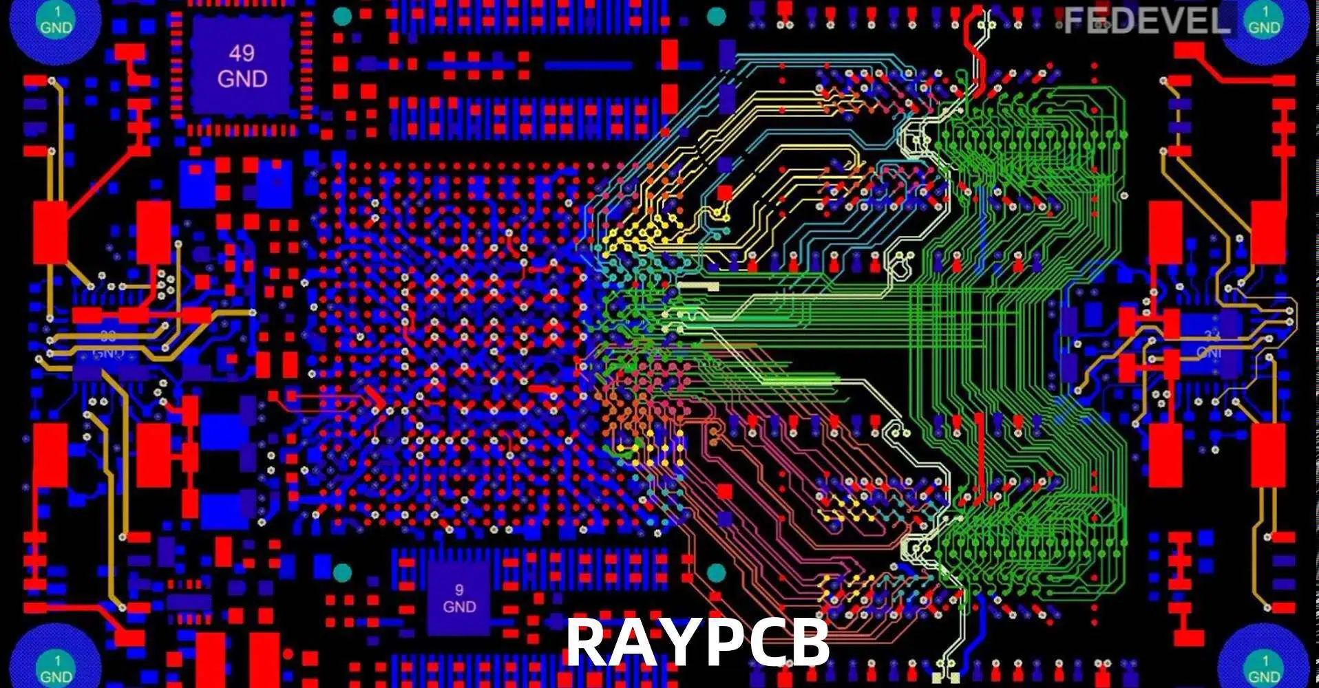
Computer-Aided Manufacturing (CAM) has revolutionized the electronics design and production landscape. Circuit CAM represents a critical interface between electronic design automation (EDA) and manufacturing processes, enabling precise translation of circuit designs into physical manufacturing instructions.
Understanding Circuit CAM Fundamentals
What is Circuit CAM?
Circuit CAM is specialized software that transforms electronic design files into manufacturing-ready instructions for printed circuit board (PCB) production. It serves as a crucial bridge between design conceptualization and physical manufacturing, ensuring accuracy and efficiency in the production process.
Q1: What is the primary difference between EDA and CAM software?
A1: Electronic Design Automation (EDA) focuses on design creation, while Computer-Aided Manufacturing (CAM) translates those designs into precise manufacturing instructions, bridging the gap between conceptual design and physical production.
Q2: How often should Circuit CAM software be updated?
A2: Recommended update frequency is quarterly or with each major version release. Always ensure compatibility with your specific manufacturing equipment and design requirements.
Q3: Can Circuit CAM handle complex multilayer PCB designs?
A3: Modern Circuit CAM solutions are designed to manage intricate multilayer designs with advanced layer management, registration, and alignment capabilities.
Q4: What file formats are typically supported by Circuit CAM?
A4: Standard supported formats include Gerber (RS-274X), ODB++, DXF, AutoCAD, and various proprietary EDA tool export formats.
Q5: How do I ensure optimal manufacturing results with Circuit CAM?
A5: Ensure comprehensive design rule checking, maintain updated software, perform regular calibrations, and invest in continuous training for design and manufacturing teams.
Conclusion
Circuit CAM represents a sophisticated intersection of design intelligence and manufacturing precision. By understanding its comprehensive capabilities, engineers and manufacturers can transform complex electronic designs into high-quality, reliable products with unprecedented efficiency.
The synchronization between PADS Logic and PADS Layout ensures design consistency throughout the PCB development process. Proper synchronization prevents errors, reduces design time, and maintains data integrity between schematic and layout phases.
Q5: How do I handle partial updates during synchronization?
A: For partial updates:
Use selective synchronization
Create specific ECOs
Verify affected areas
Document changes
Test functionality
Update related documentation
Conclusion
Successful synchronization between PADS Logic and Layout requires careful attention to detail, consistent procedures, and regular verification. By following these guidelines and best practices, you can maintain design integrity throughout the PCB development process. Remember to regularly backup your work, document changes, and verify synchronization results to ensure successful project completion.
PCB fabrication drawings, also known as PCB mechanical drawings or PCB assembly drawings, are essential technical documents that provide detailed specifications for manufacturing printed circuit boards. These drawings serve as a communication bridge between PCB designers and manufacturers, ensuring accurate production of the intended design.
Q1: What are the most important elements to check in a PCB fabrication drawing?
A: The critical elements to verify include:
Board dimensions and tolerances
Layer stack-up details
Drill specifications
Material requirements
Surface finish specifications
Special notes and requirements Always cross-reference these with your manufacturer’s capabilities.
Q2: How do I interpret drill table symbols and specifications?
A: Drill tables typically include:
Drill size (diameter)
Quantity of each size
Plating requirements (PTH/NPTH)
Special requirements (depth for blind vias)
Tolerance specifications Look for the corresponding symbols on the drawing to locate each hole type.
Q3: What is the significance of the layer stack-up table?
A: The layer stack-up table defines:
Number of copper layers
Layer thicknesses
Material types
Dielectric specifications
Overall board thickness This information is crucial for impedance control and manufacturing process planning.
Q4: How do I verify dimensional tolerances?
A: To verify tolerances:
Check the general tolerance note
Look for specific critical tolerances
Compare with manufacturer capabilities
Consider cumulative tolerances
Verify against assembly requirements
Q5: What common mistakes should I watch for when reading fabrication drawings?
A: Common oversights include:
Missing or incorrect revision numbers
Conflicting specifications
Unclear special requirements
Incomplete drill information
Missing critical dimensions Always cross-reference with other documentation and verify completeness.
Conclusion
Reading PCB fabrication drawings requires attention to detail and understanding of various technical specifications. The ability to interpret these drawings accurately is crucial for successful PCB manufacturing. Always verify critical parameters, cross-reference specifications with manufacturer capabilities, and ensure all special requirements are clearly communicated. When in doubt, consult with your PCB manufacturer for clarification on any aspects of the fabrication drawing.
Microvia failures primarily stem from thermal stresses induced during PCB assembly processes. These stresses can critically compromise the structural integrity of plated interconnects, leading to reduced product lifespan. To enhance microvia reliability, designers should implement three key strategies:
Material selection optimized for laser drilling processes
Strict compliance with IPC-T-50M specifications for via formation
Careful stack-up design following IPC-2226 guidelines for HDI structures
These measures collectively address the thermo-mechanical challenges inherent in high-density interconnect designs.
What are Microvias?
Before we dive into the specifics of designing reliable microvias, it’s essential to understand what microvias are and their role in modern PCB design.
Definition and Characteristics
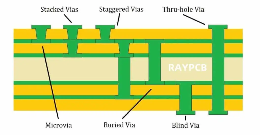
Microvias are small holes drilled in a PCB that connect different layers of the board. Unlike traditional through-holes or vias, microvias are significantly smaller, typically with a diameter of 150 micrometers (μm) or less. They are crucial components in HDI boards, allowing for higher component density and improved signal integrity.
Types of Microvias
There are several types of microvias, each with its own characteristics and applications:
Blind Microvias: These connect an outer layer to one or more inner layers but do not extend through the entire board.
Buried Microvias: These are internal connections that do not reach any outer layer of the PCB.
Stacked Microvias: These are a series of microvias placed directly on top of each other, connecting multiple layers.
Staggered Microvias: These are offset from each other rather than stacked directly on top of one another.
Understanding these different types is crucial for designing reliable microvias, as each type has its own set of design considerations and potential failure modes.
3 Primary Factors That Contribute to Microvia Failure
Microvia failure can have severe consequences for the functionality and reliability of HDI boards. Three primary factors often contribute to these failures:
1. Usage of High-Temperature Dielectric Materials
High-temperature dielectric materials are often used in PCB manufacturing to improve the board’s thermal performance. However, these materials can pose challenges for microvia reliability:
Thermal Expansion: High-temperature materials may have different coefficients of thermal expansion (CTE) compared to the copper used in microvias, leading to stress during thermal cycling.
Drilling Challenges: Some high-temperature materials can be more difficult to drill accurately, potentially compromising microvia formation.
To mitigate these issues:
Carefully select dielectric materials that balance thermal performance with microvia reliability.
Consider using laser-drillab
le materials specifically designed for HDI applications.
2. Expansion Rate Mismatch
The mismatch in thermal expansion rates between different materials in the PCB stack-up can lead to significant stress on microvias:
Copper vs. Dielectric: The difference in CTE between copper and the surrounding dielectric material can cause stress during thermal cycling.
Plating Materials: The choice of plating materials for microvias can also impact the overall expansion rate mismatch.
To address this factor:
Choose materials with compatible CTEs when possible.
Use design techniques like staggered microvias to distribute stress more evenly.
Consider thermal simulations to predict and mitigate expansion-related issues.
3. Multiple Lamination Cycles
HDI boards often require multiple lamination cycles during manufacturing, which can impact microvia reliability:
Thermal Stress: Each lamination cycle exposes the board to high temperatures, potentially stressing existing microvias.
Material Degradation: Repeated heating can degrade some PCB materials, affecting their electrical and mechanical properties.
To minimize the impact of multiple lamination cycles:
Optimize the PCB stack-up to reduce the number of required lamination cycles.
Use materials specifically designed to withstand multiple lamination processes.
Consider sequential lamination techniques to protect earlier-formed microvias.
What Leads to Microvia Failure During the Reflow Process?
The reflow process, essential for surface mount technology (SMT) assembly, can be particularly challenging for microvias. Several factors can contribute to microvia failure during reflow:
1. Thermal Shock
The rapid temperature changes during reflow can cause thermal shock, leading to:
As mentioned earlier, the difference in thermal expansion rates becomes particularly problematic during reflow:
Stress concentration at the microvia barrel
Potential separation between the microvia and surrounding materials
3. Moisture Sensitivity
Absorbed moisture can expand rapidly during reflow, causing:
Internal pressure build-up
Delamination or “popcorning” effect
4. Insufficient Copper Plating
Inadequate copper plating in microvias can lead to:
Weak connections that fail under thermal stress
Increased susceptibility to fatigue failure
5. Voiding
Voids in the microvia fill material or plating can expand during reflow, causing:
Cracking or separation
Increased electrical resistance
To mitigate these issues, careful consideration must be given to material selection, manufacturing processes, and design strategies, as we’ll explore in the next section.
5 Tips to Design Reliable Microvias
Designing reliable microvias requires a multifaceted approach, considering materials, standards, and manufacturing processes. Here are five essential tips to ensure the reliability of your microvia designs:
1. Pick a Dielectric Material Suitable for Laser Drilling
The choice of dielectric material is crucial for microvia reliability:
Laser-Friendly Materials: Opt for materials specifically designed for laser drilling, such as high-Tg (glass transition temperature) epoxies or liquid crystal polymers (LCPs).
Controlled CTE: Choose materials with a coefficient of thermal expansion (CTE) that closely matches that of copper to minimize stress.
Consider Signal Integrity: Select materials with appropriate dielectric constants and loss tangents for your application’s frequency requirements.
Key considerations:
Laser ablation characteristics
Thermal stability
Electrical properties
2. Adhere to IPC-T-50M Microvia Standards
The IPC-T-50M standard provides crucial guidelines for microvia design:
Size Definitions: Follow the standard’s definitions for microvia dimensions (typically ≤150μm in diameter).
Aspect Ratio: Adhere to recommended aspect ratios (depth to width) for different microvia types.
Terminology: Use standardized terminology to ensure clear communication with manufacturers and other stakeholders.
Benefits of adherence:
Improved manufacturability
Better consistency across different manufacturers
Enhanced reliability through proven design practices
3. Prefer Staggered Microvias Over Stacked
While stacked microvias can save space, staggered designs often offer better reliability:
Stress Distribution: Staggered microvias distribute stress more evenly across the board.
Improved Plating: Easier to achieve consistent plating in staggered configurations.
Enhanced Reliability: Less susceptible to cumulative stress failures.
Design considerations:
Balance between density requirements and reliability
Signal integrity implications of staggered vs. stacked designs
Manufacturing capabilities and preferences
4. Choose a Stack-Up in Accordance with IPC 2226 Standards
Powered By EmbedPress
IPC 2226 provides comprehensive guidelines for HDI PCB design, including stack-up recommendations:
IPC-2226 Type I
Characteristics: Single microvia layer on each side of the core.
Advantages: Simpler manufacturing, good for moderate density requirements.
IPC-2226 Type II
Characteristics: Multiple microvia layers on each side of the core.
Advantages: Higher density than Type I, still relatively straightforward to manufacture.
IPC-2226 Type III with Stacked Microvias
Characteristics: Microvias connect three or more layers.
Advantages: Very high density, suitable for complex designs.
Considerations: Requires careful design and manufacturing to ensure reliability.
IPC-2226 Type III with Staggered Microvias
Characteristics: Microvias connect multiple layers but are offset rather than stacked.
Advantages: Better reliability than stacked microvias, still achieves high density.
IPC-2226 Type III with Filled, Capped, and Staggered Microvias
Characteristics: Microvias are filled with conductive or non-conductive material and capped with plated copper.
Advantages: Highest reliability, suitable for the most demanding applications.
Considerations: More complex and costly to manufacture.
Choosing the right stack-up:
Consider your density requirements
Evaluate manufacturing capabilities and costs
Assess the reliability needs of your application
5. Ensure Zero Clearance Between the Solder Mask and Microvia
Proper solder mask design is crucial for microvia reliability:
Zero Clearance: Design the solder mask to have zero clearance with the microvia, covering the entire top surface of the via.
Benefits:
Prevents solder from wicking into the microvia during assembly
Reduces stress on the microvia during thermal cycling
Improves overall reliability of the connection
Implementation considerations:
Work closely with your PCB manufacturer to ensure their process can achieve zero clearance consistently.
Consider the impact on impedance control and signal integrity.
Evaluate the need for via-in-pad designs and their implications on solder mask application.
Designing Test Coupons for Testing Microvia Reliability
Test coupons are essential tools for verifying the reliability of your microvia design. They allow for destructive testing without sacrificing actual production boards. Here’s how to design effective test coupons:
1. Representative Design
Include microvias of all types and sizes used in your actual design.
Replicate the stack-up and materials of the production board.
2. Worst-Case Scenarios
Include areas with the highest density of microvias.
Incorporate the most challenging aspect ratios and stack-ups.
3. Daisy Chain Patterns
Design daisy chain patterns to allow for easy electrical testing of microvia connections.
Include patterns that isolate different microvia types and layers.
4. Thermal Stress Indicators
Include features that can help assess thermal stress, such as strategically placed PTHs (Plated Through Holes).
5. Cross-Section Targets
Design specific areas intended for cross-sectioning analysis.
Include alignment marks to ensure accurate cross-sectioning.
6. Standardization
Follow IPC-2221B guidelines for coupon design when applicable.
Ensure consistency in coupon design across different board designs for comparability.
Fabrication Notes for Microvia Reliability Testing
When submitting your design for fabrication and reliability testing, clear communication with your manufacturer is crucial. Consider the following aspects:
1. Manufacturing Capability
Specify Microvia Requirements: Clearly communicate the microvia sizes, aspect ratios, and types used in your design.
Discuss Plating Processes: Ensure the manufacturer can achieve the required plating thickness and quality, especially for high aspect ratio microvias.
Align on Inspection Methods: Agree on the methods for inspecting microvia formation and plating quality.
2. Cost Considerations
Balance Reliability and Cost: Understand the cost implications of different microvia designs and reliability testing methods.
Volume Considerations: Discuss how reliability testing requirements might change based on production volume.
Test Coupon Quantities: Determine the appropriate number of test coupons to balance cost and statistical significance.
3. Specific Testing Requirements
Thermal Cycling Parameters: Specify the number of cycles, temperature range, and dwell times for thermal cycling tests.
Electrical Testing Criteria: Define the pass/fail criteria for electrical continuity tests.
Cross-Sectioning Requirements: Specify the locations and number of cross-sections required.
4. Documentation
Provide Detailed Fabrication Notes: Include specific instructions for microvia formation, plating, and any special processes.
Reference Standards: Clearly reference any IPC or other industry standards that should be followed.
Request Test Reports: Specify the format and content of reliability test reports you expect to receive.
IPC-TM-650 Test Methods for Microvia Reliability
The IPC-TM-650 test methods provide standardized procedures for assessing the reliability of microvias. Here are some key test methods relevant to microvia reliability:
While focused on PTHs, this method provides a framework for reliability reporting that can be adapted for microvias:
Content: Includes details on test conditions, results, and statistical analysis.
Importance: Ensures comprehensive and standardized reliability reporting.
5. Method 3.6.2: Etching, Microsection
This method is crucial for analyzing microvia structure:
Procedure: Involves cross-sectioning and etching to reveal microvia details.
Assessment: Allows for detailed examination of microvia formation, plating quality, and potential failure modes.
Conclusion
Designing reliable microvias for high-density PCBs is a complex but crucial task in modern electronics manufacturing. By understanding the factors that contribute to microvia failure, implementing best design practices, and utilizing appropriate testing methods, engineers can create HDI boards that meet the demanding requirements of today’s electronic devices.
Key takeaways for ensuring microvia reliability include:
Careful material selection, particularly for dielectric materials
Adherence to IPC standards for microvia design and stack-up
Preference for staggered microvia designs when possible
Proper solder mask application with zero clearance
Comprehensive reliability testing using well-designed test coupons
As technology continues to advance, the importance of reliable microvia design will only grow. By staying informed about the latest standards, materials, and manufacturing techniques, PCB designers can create high-density boards that not only meet current needs but are also prepared for the challenges of future electronic designs.
Remember, successful microvia design is not just about following rules but understanding the underlying principles and making informed decisions based on your specific application requirements. Collaboration between designers, manufacturers, and test engineers is essential to achieve the highest levels of microvia reliability in high-density PCBs.
In the ever-evolving world of electronics, the demand for smaller, more powerful devices continues to grow. To meet these demands, printed circuit board (PCB) manufacturers are constantly seeking ways to increase integration density. One of the most effective techniques for achieving this goal is the use of blind microvias. This article will explore the concept of blind microvias, their benefits, and how they can be leveraged to significantly increase PCB integration density.
What Are Blind Microvias?
Definition and Basic Concepts
Blind microvias are small, laser-drilled holes in a PCB that connect one outer layer to one or more inner layers, but do not extend through the entire board. These tiny interconnects, typically less than 150 micrometers in diameter, allow for more efficient use of PCB real estate and enable higher component density.
Blind microvias: Connect an outer layer to one or more inner layers
Buried microvias: Connect inner layers only
Through microvias: Extend through the entire PCB
This article focuses primarily on blind microvias due to their significant impact on increasing integration density.
Advantages of Blind Microvias
Increased Circuit Density
The primary advantage of blind microvias is their ability to dramatically increase circuit density. By allowing connections between layers without passing through the entire board, designers can place components and routing channels more efficiently.
Improved Signal Integrity
Blind microvias offer shorter signal paths compared to traditional through-hole vias. This reduction in path length leads to:
These factors contribute to better overall electrical performance, especially in high-frequency applications.
Space Savings
Blind microvias occupy less space than traditional through-hole vias, freeing up valuable real estate on the PCB for additional components or routing channels.
Implementing Blind Microvias for Increased Integration Density
Design Considerations
When implementing blind microvias to increase integration density, several design factors must be considered:
1. Layer Stack-up
The layer stack-up is crucial in determining the effectiveness of blind microvias. A well-designed stack-up can maximize the benefits of blind microvias while minimizing manufacturing complexities.
2. Aspect Ratio
The aspect ratio (depth-to-diameter ratio) of blind microvias is a critical factor in their reliability and manufacturability. Generally, lower aspect ratios are preferred for improved reliability and easier manufacturing.
3. Pad and Anti-pad Sizes
Optimizing pad and anti-pad sizes is essential for maximizing routing space while maintaining reliable connections.
4. Microvia Placement
Strategic placement of blind microvias can significantly impact the overall integration density. Designers should consider factors such as signal paths, power distribution, and thermal management when determining microvia locations.
Manufacturing Processes
Laser Drilling
Laser drilling is the most common method for creating blind microvias. This process offers several advantages:
High precision
Ability to create very small diameter holes
Minimal damage to surrounding materials
Filling and Plating
After drilling, blind microvias are typically filled with conductive material and plated to ensure reliable electrical connections. Common filling materials include:
Copper
Conductive epoxy
Non-conductive epoxy (with subsequent plating)
Design Rules and Best Practices
To maximize the benefits of blind microvias while ensuring manufacturability and reliability, consider the following design rules and best practices:
Maintain a minimum distance between microvias to prevent structural weakening of the PCB
Use staggered microvia patterns to distribute stress more evenly
Avoid placing microvias directly on top of each other in consecutive layers
Consider thermal management when placing microvias near high-power components
Use appropriate pad and anti-pad sizes to balance reliability and routing space
Impact on PCB Integration Density
The use of blind microvias can significantly increase PCB integration density. To illustrate this impact, consider the following comparison table:
Metric
Traditional Through-Hole Design
Design with Blind Microvias
Component Density
Baseline
Up to 50% increase
Routing Channels
Baseline
Up to 30% increase
Layer Count
Baseline
Potential reduction of 20-30%
Signal Integrity
Baseline
Improved (shorter paths)
Manufacturing Complexity
Low
Moderate to High
Cost
Baseline
10-30% increase
As the table shows, the use of blind microvias can lead to significant improvements in component density and routing efficiency, potentially allowing for a reduction in the overall layer count of the PCB.
Challenges and Considerations
While blind microvias offer numerous advantages, there are also challenges to consider:
Manufacturing Complexity
The creation of blind microvias requires specialized equipment and processes, which can increase manufacturing complexity and cost.
Reliability Concerns
Blind microvias can be more susceptible to reliability issues such as:
These concerns can be mitigated through proper design and manufacturing processes.
Cost Considerations
The implementation of blind microvias typically increases PCB manufacturing costs. However, this increase is often offset by the benefits of higher integration density and potential reductions in overall board size or layer count.
Future Trends in Microvia Technology
As the electronics industry continues to demand higher levels of integration, microvia technology is expected to evolve. Some emerging trends include:
Smaller diameter microvias (sub-50 μm)
Higher aspect ratio microvias
Improved filling and plating materials
Advanced inspection and testing methods
Integration with other advanced PCB technologies (e.g., embedded components)
Case Studies: Successful Implementation of Blind Microvias
Case Study 1: Mobile Device PCB
A manufacturer of high-end smartphones implemented blind microvias in their main board design, resulting in:
40% increase in component density
25% reduction in board size
Improved signal integrity in high-speed data lines
Case Study 2: Aerospace Application
An aerospace company utilized blind microvias in a mission-critical control system PCB, achieving:
30% reduction in overall weight
20% improvement in thermal management
Enhanced reliability in high-vibration environments
Conclusion
qrf
Blind microvias represent a powerful tool for increasing the integration density of PCBs. By enabling more efficient use of board real estate, improving signal integrity, and enhancing overall electrical performance, blind microvias allow designers to create smaller, more powerful electronic devices. While challenges exist in terms of manufacturing complexity and cost, the benefits often outweigh these concerns, particularly in applications where size and performance are critical factors.
As the electronics industry continues to push the boundaries of miniaturization and performance, the role of blind microvias in PCB design is likely to become increasingly important. By understanding the advantages, challenges, and best practices associated with this technology, PCB designers and manufacturers can leverage blind microvias to create cutting-edge electronic products that meet the demands of tomorrow’s markets.
Frequently Asked Questions (FAQ)
Q1: What is the minimum size of a blind microvia?
A1: The minimum size of a blind microvia typically ranges from 50 to 150 micrometers in diameter. However, some advanced manufacturing processes can produce microvias with diameters as small as 25 micrometers. The specific minimum size depends on factors such as the PCB material, layer count, and manufacturing capabilities.
Q2: How do blind microvias compare to buried vias in terms of increasing integration density?
A2: Both blind and buried microvias can increase integration density, but they serve different purposes. Blind microvias connect outer layers to inner layers, while buried vias connect only inner layers. Blind microvias are generally easier to manufacture and inspect, making them more common for increasing density. However, a combination of both types can often achieve the highest level of integration density in complex designs.
Q3: Are there any specific industries or applications where blind microvias are particularly beneficial?
A3: Blind microvias are particularly beneficial in industries requiring high-density, high-performance electronics in small form factors. Some key applications include:
Automotive electronics (especially in electric and autonomous vehicles)
Q4: What are the main reliability concerns with blind microvias, and how can they be addressed?
A4: The main reliability concerns for blind microvias include:
Fatigue cracking due to thermal cycling
Delamination
Incomplete filling or plating
Electrical opens or shorts
These issues can be addressed through:
Proper design (e.g., optimizing aspect ratios, using staggered patterns)
High-quality manufacturing processes
Appropriate material selection
Rigorous testing and inspection procedures
Adhering to industry standards and best practices
Q5: How does the cost of PCBs with blind microvias compare to traditional designs?
A5: PCBs with blind microvias generally have higher manufacturing costs compared to traditional designs, typically ranging from 10% to 30% more expensive. However, this cost increase is often offset by:
Reduced overall board size
Potential reduction in layer count
Improved performance and reliability
Enablement of more compact and feature-rich products
When considering the total cost of the end product and its performance benefits, designs incorporating blind microvias can often be more cost-effective in the long run, especially for high-value or high-performance applications.
Designing a printed circuit board (PCB) goes beyond simply connecting components—it’s about engineering a product that is reliable, manufacturable, and compliant with industry best practices. This is where IPC standards play a crucial role.
As the most widely recognized guidelines in electronics manufacturing, IPC standards define the design, fabrication, and assembly requirements that ensure PCBs perform consistently across industries—from consumer electronics to aerospace and defense. These standards influence everything from trace width and spacing to thermal management and material selection, helping designers avoid costly errors and production delays.
The primary objective of IPC standards is to guarantee safety, reliability, and manufacturability in electronic products. Whether you’re developing medical devices, automotive systems, or industrial equipment, adhering to IPC guidelines helps meet regulatory requirements, reduce defects, and improve overall product quality.
Understanding IPC Standards for PCB Design
IPC, formerly known as the Institute for Printed Circuits and now as the Association Connecting Electronics Industries, is a global trade association that sets the standards for the electronic interconnect industry. IPC Standards for PCB Design are a set of guidelines and requirements that ensure consistency, quality, and reliability in PCB production across the industry.
Why IPC Standards Matter in PCB Design
IPC Standards play a crucial role in the PCB industry for several reasons:
Quality Assurance: They provide a benchmark for quality, ensuring that PCBs meet specific performance and reliability criteria.
Consistency: Standards enable consistency across different manufacturers and suppliers, facilitating easier collaboration and interoperability.
Cost Reduction: By following standardized practices, manufacturers can reduce errors, rework, and waste, ultimately lowering production costs.
Innovation: Standards provide a foundation upon which new technologies and design techniques can be built and integrated.
Global Communication: IPC Standards serve as a common language for the industry, improving communication between designers, manufacturers, and customers worldwide.
Powered By EmbedPress
Key IPC Standards for PCB Design
Let’s explore some of the most important IPC Standards that directly impact PCB design:
IPC-2220 Series: Design Standards
The IPC-2220 series is fundamental to PCB design, covering various aspects of the design process.
IPC-2221: Generic Standard on Printed Board Design
This standard provides general requirements for the design of printed boards and forms the foundation for other design standards in the series.
Key aspects covered:
Material selection
Electrical and mechanical considerations
Thermal management
Design for manufacturability (DFM)
Documentation requirements
IPC-2222: Sectional Design Standard for Rigid Organic Printed Boards
This standard focuses specifically on the design of rigid organic printed boards, building upon the general requirements outlined in IPC-2221.
Areas of focus:
Layer stackup considerations
Conductor spacing and width requirements
Via and hole design rules
Soldermask and silkscreen guidelines
IPC-2223: Sectional Design Standard for Flexible Printed Boards
For designers working with flexible PCBs, this standard provides specific guidelines and requirements.
Key topics:
Flexible material selection and properties
Bend radius considerations
Dynamic flexing requirements
Adhesive selection and application
IPC-2226: Sectional Design Standard for High Density Interconnect (HDI) Printed Boards
As PCB designs become increasingly complex and miniaturized, HDI technology has become crucial. This standard addresses the specific requirements for HDI PCB design.
Important aspects:
Microvia design and fabrication
Fine line and space requirements
Stacked and staggered via structures
Laser drilling considerations
IPC-6010 Series: Performance Specifications
While the IPC-2220 series focuses on design, the IPC-6010 series sets the performance specifications for finished PCBs.
IPC-6011: Generic Performance Specification for Printed Boards
This standard establishes the general performance requirements for PCBs, regardless of their specific type or application.
Key areas covered:
Electrical performance criteria
Mechanical integrity requirements
Environmental resistance specifications
Marking and traceability guidelines
IPC-6012: Qualification and Performance Specification for Rigid Printed Boards
Hardware Layout
Building on IPC-6011, this standard provides specific performance requirements for rigid PCBs.
Important aspects:
Dimensional and physical property requirements
Solderability and resistance to soldering heat
Thermal stress resistance
Cleanliness requirements
IPC-6013: Qualification and Performance Specification for Flexible Printed Boards
For flexible PCBs, this standard outlines the specific performance criteria that must be met.
Key topics:
Flexibility and endurance requirements
Adhesion strength specifications
Dimensional stability under various conditions
Specialized testing procedures for flexible circuits
IPC-7351: Generic Requirements for Surface Mount Design and Land Pattern Standard
This standard is crucial for designers working with surface mount technology (SMT), which is prevalent in modern PCB designs.
Understanding IPC Standards is one thing, but implementing them effectively in your PCB design workflow is another. Here are some best practices for incorporating IPC Standards into your design process:
1. Education and Training
Ensure that your design team is well-versed in the relevant IPC Standards:
Conduct regular training sessions on IPC Standards updates
Encourage designers to obtain IPC certifications
Maintain a library of IPC Standards documentation for easy reference
2. Design Rule Implementation
Integrate IPC Standards into your design rules within your PCB design software:
Set up design rule checks (DRCs) based on IPC specifications
Create custom design rule sets for different product classes (Class 1, 2, or 3)
Regularly update these rules as standards evolve
3. Component Library Management
Maintain a component library that adheres to IPC Standards:
Use IPC-compliant footprints for surface mount components
Include IPC-recommended land patterns in your library
Regularly audit and update your component library to ensure ongoing compliance
4. Design for Manufacturability (DFM)
Incorporate DFM principles based on IPC Standards:
Follow IPC guidelines for conductor spacing, width, and clearances
Adhere to IPC recommendations for via and hole design
Consider IPC-defined material properties in your stackup design
5. Documentation and Specifications
Ensure your design documentation aligns with IPC Standards:
Use IPC-specified drawing formats and symbols
Include IPC-recommended fabrication and assembly notes
Clearly specify which IPC Standards and classes apply to your design
6. Collaboration with Manufacturers
Work closely with your PCB manufacturers to ensure IPC Standard compliance:
Communicate which IPC Standards are applicable to your design
Request IPC-compliant manufacturing processes
Discuss any deviations from IPC Standards and their potential impacts
Use IPC-defined test methods for electrical and mechanical verification
Adhere to IPC cleanliness and inspection criteria
Maintain records of compliance and any non-conformances
Advanced Topics in IPC Standards for PCB Design
As PCB technology continues to advance, IPC Standards evolve to address new challenges and opportunities. Let’s explore some advanced topics covered by IPC Standards:
High-Speed and High-Frequency Design
With the increasing prevalence of high-speed digital and RF applications, IPC has developed standards to address these specialized design requirements:
IPC-2251: Design Guide for the Packaging of High Speed Electronic Circuits
This guide provides recommendations for designing high-speed PCBs, covering topics such as:
Impedance control techniques
Signal integrity considerations
Power distribution network (PDN) design
EMI/EMC mitigation strategies
IPC-2141: Design Guide for High-Speed Controlled Impedance Circuit Boards
Focused specifically on controlled impedance design, this guide covers:
Test and verification methods for controlled impedance
Embedded Components Technology
As PCB designs become more compact and integrated, embedded component technology is gaining traction. IPC has responded with standards addressing this emerging field:
IPC-7092: Design and Assembly Process Implementation for Embedded Components
This standard provides guidelines for designing PCBs with embedded passive and active components, covering:
Design considerations for embedding components
Material selection for embedded component PCBs
Manufacturing process requirements
Reliability and testing considerations
Additive Manufacturing for PCBs
3D printing technology is making inroads into PCB manufacturing, prompting the development of new standards:
IPC-4921: Requirements for Printed Electronics Base Materials
While not specific to additive manufacturing, this standard lays the groundwork for materials used in emerging PCB fabrication technologies, including:
Material properties for printed electronics
Test methods for printed electronic materials
Performance requirements for various applications
The Future of IPC Standards for PCB Design
As technology continues to evolve at a rapid pace, IPC Standards must adapt to remain relevant and effective. Here are some areas where we can expect to see developments in IPC Standards for PCB Design:
1. Internet of Things (IoT) and Wearable Devices
The proliferation of IoT and wearable devices presents new challenges in terms of miniaturization, flexibility, and durability. Future IPC Standards may address:
Integration of sensors and antennas in PCB designs
Durability standards for wearable electronics
2. 5G and Beyond
As 5G technology rolls out and research into 6G begins, PCB designs for high-frequency applications will become increasingly important. Future standards may focus on:
The integration of AI and ML capabilities into PCB designs may lead to new standards addressing:
Design considerations for AI accelerator chips
Thermal management for high-performance computing PCBs
Power distribution for AI-enabled devices
4. Sustainability and Environmental Considerations
As environmental concerns become more pressing, future IPC Standards may place greater emphasis on:
Design for recyclability and circular economy principles
Use of sustainable and biodegradable materials in PCB manufacturing
Energy efficiency in PCB design and production
5. Quantum Computing
As quantum computing technology advances, specialized PCB designs will be required. Future IPC Standards may need to address:
Ultra-low temperature PCB designs for quantum circuits
Specialized materials for quantum-compatible PCBs
Unique testing and verification procedures for quantum PCBs
Challenges in Implementing IPC Standards for PCB Design
While IPC Standards provide numerous benefits, their implementation can present challenges for PCB designers and manufacturers:
1. Keeping Up with Revisions
IPC Standards are regularly updated to reflect technological advancements and industry needs. Staying current with these revisions can be challenging:
Allocate resources for ongoing education and training
Implement a system for tracking and implementing standard updates
Regularly review and update internal design guidelines
2. Balancing Standards with Innovation
Sometimes, cutting-edge designs may push the boundaries of existing standards:
Develop processes for evaluating and justifying deviations from standards
Engage with IPC committees to provide feedback on emerging design needs
Document and share experiences to contribute to future standard revisions
3. Cost of Compliance
Adhering to IPC Standards can sometimes increase design and manufacturing costs:
Conduct cost-benefit analyses to justify standard implementation
Look for opportunities to streamline processes through standardization
Consider the long-term benefits of improved quality and reliability
4. Global Variations
While IPC Standards are widely recognized, some regions may have additional or differing requirements:
Be aware of regional variations in standards and regulations
Develop flexible design processes that can adapt to different requirements
Foster communication between global design teams to share best practices
5. Complexity in Multi-Board Systems
Modern electronic products often involve multiple interconnected PCBs, which can complicate standards compliance:
Develop system-level design guidelines that incorporate IPC Standards
Consider the interplay between different board types (rigid, flex, rigid-flex) in a single system
Implement comprehensive testing procedures for multi-board assemblies
Conclusion: The Vital Role of IPC Standards in PCB Design
IPC Standards for PCB Design play a crucial role in ensuring the reliability, performance, and interoperability of electronic devices in our increasingly connected world. By providing a common framework for design, manufacturing, and quality assurance, these standards enable the electronics industry to meet the ever-growing demands for smaller, faster, and more complex devices.
As we’ve explored in this comprehensive guide, IPC Standards cover a wide range of topics, from basic design principles to advanced technologies like high-speed design and embedded components. By implementing these standards in your PCB design workflow, you can:
Improve the quality and reliability of your PCB designs
Enhance communication and collaboration with manufacturers and suppliers
Reduce costs associated with errors, rework, and production issues
Stay at the forefront of technological advancements in the PCB industry
However, it’s important to remember that IPC Standards are not static. They continue to evolve alongside technological advancements, addressing new challenges and opportunities in areas such as IoT, 5G, AI, and beyond. As a PCB designer or manufacturer, staying informed about these evolving standards and actively participating in their development is key to remaining competitive in the industry.
Ultimately, the judicious application of IPC Standards for PCB Design is not just about compliance – it’s about creating better, more reliable electronic products that can meet the demands of today’s technology-driven world. By embracing these standards and integrating them into your design philosophy, you can ensure that your PCB designs are not just meeting the minimum requirements, but are positioned to excel in performance, reliability, and manufacturability.
As we look to the future, the role of IPC Standards in PCB design will only grow in importance. By staying committed to these standards and contributing to their ongoing development, the PCB design community can continue to push the boundaries of what’s possible in electronics, driving innovation and shaping the technologies that will define our future.
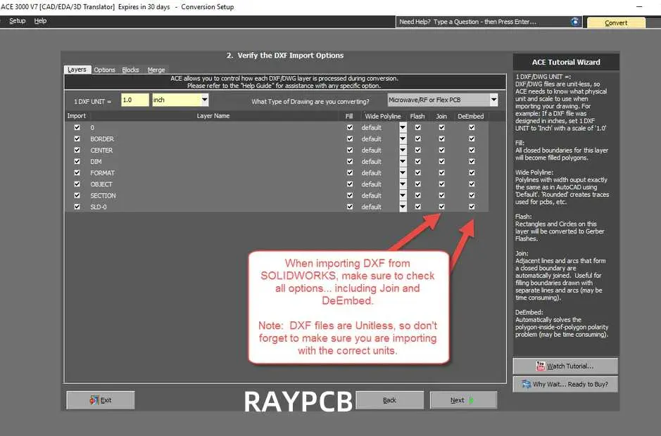
In the world of Computer-Aided Design (CAD) and Printed Circuit Board (PCB) manufacturing, file formats play a crucial role in ensuring smooth workflows and accurate production. Two file formats that frequently intersect in these industries are DXF (Drawing Exchange Format) and Gerber. While both are used to represent design data, they serve different purposes and are often required to be converted from one to the other. This comprehensive guide will explore the intricacies of DXF to Gerber and Gerber to DXF conversion, providing you with the knowledge and tools necessary to navigate this essential process.
DXF files, developed by Autodesk, are widely used in CAD software for exchanging drawing information. On the other hand, Gerber files are the standard format for PCB manufacturing, containing the necessary data for producing circuit boards. The need to convert between these formats arises when designers want to bring CAD designs into PCB software or when PCB designs need to be modified in CAD programs.
While the conversion process can present challenges, such as maintaining accuracy and preserving design intent, numerous solutions exist to facilitate smooth transitions between DXF and Gerber formats. This article will delve into the best tools, online converters, and free solutions available for both DXF to Gerber and Gerber to DXF conversions, ensuring you have the resources needed to tackle your design projects effectively.
Before diving into the conversion process, it’s essential to understand the nature and purpose of both DXF and Gerber files.
What is a DXF file?
DXF (Drawing Exchange Format) is a CAD data file format developed by Autodesk to enable data interoperability between AutoCAD and other programs. Key characteristics of DXF files include:
Vector-based format, allowing for scalable graphics without loss of quality
Supports 2D and 3D design data
Widely used in architecture, engineering, and product design
Can contain layers, line types, and other CAD-specific information
What is a Gerber file?
Gerber is the standard file format used in the PCB industry for manufacturing circuit boards. Important features of Gerber files include:
Contains information for each layer of a PCB design
Integrating PCB designs with mechanical assemblies
Understanding these use cases helps in appreciating the importance of reliable conversion methods between DXF and Gerber formats.
2. DXF to Gerber Conversion
Converting DXF files to Gerber format is a common requirement when transitioning from general CAD work to PCB design. This process involves translating vector graphics and design data into a format suitable for circuit board manufacturing.
What happens when you convert DXF to Gerber
During the conversion process, several key transformations occur:
Vector data is translated into PCB-specific entities (traces, pads, etc.)
Layers are mapped to appropriate PCB layers (e.g., copper, silkscreen)
Scale and units are adjusted to match PCB manufacturing standards
Non-PCB elements may be filtered out or require manual handling
Common use cases for DXF to Gerber conversion
Some typical scenarios where DXF to Gerber conversion is necessary include:
Creating custom PCB outlines from mechanical designs
Importing logo or graphics for silkscreen layers
Developing flex PCBs with complex shapes
Integrating PCB designs with enclosure or chassis files
Important factors to consider
When converting DXF to Gerber, keep these factors in mind:
Layer mapping: Ensure CAD layers correspond correctly to PCB layers
Scaling: Verify that dimensions are accurately preserved
Precision: Check that the conversion maintains the required level of detail
Compatibility: Ensure the resulting Gerber files meet your fabricator’s requirements
KiCAD is a popular open-source PCB design suite that can handle DXF imports:
Pros:
Free and open-source
Active community support
Regular updates and improvements
Cons:
DXF import process can be less intuitive
May require additional steps for complex conversions
EasyEDA
EasyEDA is a web-based PCB design tool with DXF import capabilities:
Pros:
User-friendly interface
Cloud-based, accessible from anywhere
Free for basic use
Cons:
Limited features compared to professional tools
May struggle with very complex DXF files
Free Software Options
FlatCAM
FlatCAM is an open-source tool specifically designed for PCB prototyping:
Pros:
Free and cross-platform
Specializes in conversions for PCB manufacturing
Supports various input and output formats
Cons:
Less polished user interface
May require some technical knowledge to use effectively
Gerbv
While primarily a Gerber viewer, Gerbv can be useful for verifying conversions:
Pros:
Free and open-source
Lightweight and fast
Good for quick visual checks
Cons:
Limited conversion capabilities
Primarily a viewer rather than a conversion tool
2.2 Online DXF to Gerber Converters
For those who prefer not to install software or need quick, one-off conversions, online tools can be a viable option. Here are some popular online converters:
EasyEDA (provides some Gerber import and DXF export capabilities)
It’s important to note that online Gerber to DXF conversion tools are less common and may not provide the same level of accuracy or features as desktop software. Always verify the results when using online converters for critical designs.
4. How to Convert Gerber to DXF: Step-by-Step Guide
For those needing to convert Gerber files to DXF format, here’s a general step-by-step guide:
1. Preparing your Gerber files
Organize your Gerber files by layer (e.g., copper, silkscreen, solder mask)
Verify that all necessary files are present, including the drill file
Check for any readme or specification files that describe the Gerber set
2. Choosing the right tool
Select a tool based on your needs (e.g., CAM350 for professional use, GerbView for simpler conversions)
Ensure the tool supports the specific Gerber format you’re working with
3. Step-by-step process for a typical Gerber to DXF conversion
Import the Gerber files into your chosen software
Verify that all layers are correctly recognized
Adjust any import settings (e.g., units, scale, layer mapping)
LibrePCB: An emerging open-source PCB design tool with growing capabilities
pcb-rnd: A fork of the gEDA PCB tool with extended features
Tips for using free tools effectively
Leverage community forums and documentation for support
Be prepared to use multiple tools in combination for best results
Contribute bug reports or improvements to help advance the tools
Verify results carefully, as free tools may have limitations
6. Common Problems and How to Solve Them
When converting between DXF and Gerber formats, several issues can arise. Here are some common problems and their solutions:
Misalignment and scaling issues
Problem: Converted design doesn’t match original dimensions Solution:
Double-check unit settings in both source and destination software
Use reference points or measurements to verify scale
Adjust scaling factors if necessary during import/export
Missing drill holes
Problem: Drill holes not appearing in converted files Solution:
Ensure drill files are included in the conversion process
Check if drill data is on a separate layer and import accordingly
Verify drill file format compatibility with your conversion tool
File corruption during conversion
Problem: Converted files appear garbled or incomplete Solution:
Try using a different conversion tool or software version
Check for any unsupported features in the original file
Simplify complex designs before conversion if possible
How to validate your files after conversion
Visual inspection: Compare original and converted files side-by-side
Layer check: Ensure all layers are present and correctly mapped
Measurements: Verify critical dimensions match the original design
Test plots: Generate plots or renders to check overall accuracy
Manufacturing check: If possible, run design rule checks or consult with a fabricator
7. Frequently Asked Questions (FAQ)
Can I convert DXF to Gerber without software?
While it’s theoretically possible to manually create Gerber files from DXF data, it’s impractical and error-prone. Using specialized software is highly recommended for accuracy and efficiency.
What’s the best free tool for Gerber to DXF?
For free Gerber to DXF conversion, KiCAD is often recommended due to its comprehensive feature set and active community support. However, the process may require multiple steps and some learning curve.
How accurate are online converters?
Online converters can be reasonably accurate for simple designs but may struggle with complex files or specialized requirements. They’re best suited for quick conversions or preliminary work, rather than final production files.
Are there risks using online file converters?
Yes, there are potential risks:
Data privacy: Your design information is uploaded to a third-party server
Intellectual property concerns: Ensure the service doesn’t claim rights to uploaded content
Accuracy: Online tools may not handle all file complexities correctly
Security: Use reputable services to minimize the risk of malware or data breaches
Always review the terms of service and privacy policy before using online conversion tools, especially for sensitive or proprietary designs.
Conclusion
Converting between DXF and Gerber formats is an essential skill for professionals working at the intersection of CAD and PCB design. While the process can present challenges, a variety of tools and methods are available to facilitate smooth conversions.
Summary of best practices
Choose the right tool for your specific needs and budget
Prepare files carefully before conversion
Pay close attention to layer mapping and scaling
Always validate converted files thoroughly
Keep up-to-date with software updates and industry standards
When to use free solutions vs. paid professional tools
Workflows that require advanced features and support
Final recommendations for CAD engineers and PCB designers
Invest time in learning at least one robust conversion tool thoroughly
Develop a standardized process for file conversion to ensure consistency
Stay informed about advancements in file formats and conversion techniques
Consider the entire design-to-manufacturing workflow when choosing conversion methods
Don’t hesitate to use multiple tools in combination for best results
Regularly backup your original files before conversion attempts
By following these guidelines and utilizing the appropriate tools, you can streamline your workflow and ensure accurate transitions between DXF and Gerber formats. Whether you’re a seasoned professional or just starting in the field, mastering these conversion techniques will prove invaluable in your CAD and PCB design projects.
Bonus: Quick Comparison Table
Here’s a quick reference table comparing key aspects of DXF to Gerber and Gerber to DXF conversions:
Feature
DXF to Gerber
Gerber to DXF
Primary Use Case
CAD to PCB
PCB back to CAD
Free Tools
FlatCAM, KiCAD
GerbView, gEDA
Online Tools
Widely available
Limited options
Main Challenges
Layer mapping, scaling
Data loss, layer reconstruction
Accuracy
Generally high
Can be less precise
Complexity
Moderate
High
Common Applications
Custom PCB shapes, mechanical layers
Reverse engineering, design modification
Industry Standard
Yes (for PCB manufacturing)
Less common
File Size
Typically smaller
Usually larger
Software Support
Widespread
More limited
This table provides a quick overview of the key differences between DXF to Gerber and Gerber to DXF conversions. It’s important to note that the specifics can vary depending on the tools and methods used.
In conclusion, while converting between DXF and Gerber formats presents certain challenges, it’s an essential process in the world of PCB design and manufacturing. By understanding the nuances of each format, utilizing the right tools, and following best practices, designers and engineers can ensure smooth transitions between CAD and PCB environments. Whether you opt for professional software, open-source solutions, or online converters, the key lies in careful preparation, meticulous validation, and a solid understanding of your project’s requirements.
The Gerber file. Among various Gerber formats, RS-274X has emerged as the industry standard, playing a crucial role in translating design into reality. This comprehensive guide aims to demystify RS-274X, exploring its intricacies, viewers, KiCAD support, and file structure.
1. What is RS-274X?
RS-274X, also known as Extended Gerber or X-Gerber, is a file format used in PCB manufacturing to describe the board layers and other essential information needed for production.
History and Evolution
The RS-274X format evolved from its predecessor, RS-274D. While RS-274D served the industry for years, it had limitations that became apparent as PCB designs grew more complex. RS-274X was introduced to address these shortcomings and provide a more robust solution for modern PCB design needs.
Why RS-274X Became the Industry Standard
RS-274X quickly became the go-to format for several reasons:
Embedded apertures: Unlike RS-274D, which required separate aperture files, RS-274X includes aperture definitions within the file itself.
Streamlined layer information: RS-274X provides a more efficient way to describe layer polarity and function.
Improved precision: The format supports higher resolution and more accurate representations of complex designs.
Wider compatibility: Most PCB design software and manufacturing equipment support RS-274X, making it a universal choice.
Key Features of RS-274X
Embedded apertures for simplified file management
Enhanced layer information handling
Support for complex pad shapes and custom apertures
Quality Control: Inspection equipment can read and verify RS-274X data
Conclusion
Understanding RS-274X is crucial for anyone involved in PCB design and manufacturing. This format, with its rich history and wide adoption, continues to be the backbone of PCB data exchange. By mastering RS-274X, you can ensure smoother workflows, fewer manufacturing errors, and ultimately, better PCB products.
Key Takeaways
Always validate your RS-274X output before sending it to manufacturers
Familiarize yourself with Gerber viewers to catch issues early
Stay informed about emerging standards while mastering RS-274X
Use tools like KiCAD to streamline your RS-274X workflow
By following these guidelines and continuously expanding your knowledge of RS-274X, you’ll be well-equipped to handle the challenges of modern PCB design and manufacturing.
FAQs
What is the difference between RS-274X and Gerber X2? RS-274X is the standard Gerber format, while Gerber X2 is an enhanced version that includes additional metadata and improved drill information.
How do I open an RS-274X file? You can open RS-274X files using Gerber viewers like Gerbv, KiCAD’s GerbView, or online tools like GerberLogix.
Is RS-274X still used in 2025? Yes, RS-274X remains widely used due to its universal compatibility and sufficient capabilities for most PCB designs.
Can I convert RS-274D files to RS-274X? Many modern EDA tools can import RS-274D files and export them as RS-274X. However, manual adjustments may be necessary to fully utilize RS-274X features.
What software best supports RS-274X? Popular EDA tools like Altium Designer, KiCAD, Eagle, and OrCAD all provide robust support for RS-274X file generation and manipulation.
The Internet of Things (IoT) refers to a vast network of interconnected electronic devices that communicate and exchange data over the internet. While consumer-facing smart devices—remotely controlled via mobile apps—are the most visible aspect of IoT, they represent just a fraction of its potential.
This comprehensive guide will walk you through the process of designing an IoT PCB, covering everything from initial layout considerations to advanced low-power optimization techniques. Whether you’re a seasoned engineer or a budding IoT enthusiast, this article will provide valuable insights into creating efficient, reliable, and cost-effective IoT circuit boards.
Design the schematic, focusing on power management and signal integrity
Create the PCB layout, optimizing for size and antenna performance
Prototype the design and perform initial testing
Iterate on the design based on test results, focusing on power optimization
Key Design Decisions and Optimizations Made
Implemented a buck-boost converter for efficient battery usage
Utilized the MCU’s low-power modes and interrupt-driven architecture
Optimized the LoRa antenna design for improved range and efficiency
Implemented a modular design for easy sensor swapping in future versions
Lessons Learned and Tips for Similar Projects
Start with a thorough power budget analysis to guide component selection
Invest time in optimizing the antenna design for better overall performance
Consider environmental factors early in the design process
Perform extensive field testing to validate real-world performance
Conclusion
Designing an IoT PCB requires a holistic approach, balancing various factors such as power efficiency, connectivity, size constraints, and reliability. By following the guidelines and best practices outlined in this article, you can create efficient, reliable, and cost-effective IoT circuit boards that form the backbone of innovative IoT devices.
Remember that successful IoT PCB design is an iterative process. Don’t hesitate to prototype, test, and refine your designs based on real-world performance data. As the IoT landscape continues to evolve, staying updated with the latest components, design techniques, and industry trends will be crucial for creating cutting-edge IoT solutions.
Whether you’re working on a simple sensor node or a complex IoT gateway, the principles of thoughtful design, careful component selection, and rigorous testing will serve you well. Embrace the challenges and opportunities that IoT PCB design presents, and you’ll be well-equipped to contribute to the exciting world of connected devices and smart systems.
In today’s rapidly evolving electronic landscape, the demand for faster, more efficient devices continues to grow exponentially. At the heart of these advancements lies a critical discipline: high speed PCB design. Modern electronic systems—from smartphones and laptops to data centers and automotive electronics—rely on printed circuit boards that can effectively handle high-speed signals while maintaining performance integrity.
High speed PCB design represents the sophisticated art and science of creating circuit boards that can reliably transmit signals at rates exceeding 1 Gbps. As clock frequencies and data rates increase, traditional PCB design approaches fall short, introducing a host of complex challenges including signal integrity issues, electromagnetic interference (EMI), and thermal management concerns.
The importance of mastering signal integrity, EMI control, and proper layout techniques cannot be overstated. When signals travel at high speeds, they behave less like simple electrical connections and more like transmission lines with complex electromagnetic properties. A minor design oversight—such as improper trace routing or inadequate grounding—can lead to significant performance degradation, intermittent failures, or complete system malfunction.
Common challenges faced by engineers in high-speed circuit design include:
Managing signal reflections and impedance discontinuities
Controlling crosstalk between adjacent traces
Mitigating electromagnetic interference
Handling propagation delays and timing issues
Selecting appropriate materials with suitable dielectric properties
Balancing performance requirements with manufacturing constraints
This comprehensive guide is intended for a wide range of professionals, including electrical engineers, PCB designers, hardware developers, and professionals working with design tools like Altium Designer and KiCad. Whether you’re designing high-speed digital circuits, RF systems, or mixed-signal boards, the principles and techniques outlined here will help you navigate the complexities of high-speed PCB design with confidence.
High speed PCB design refers to the specialized discipline of creating printed circuit boards that can reliably transmit and process signals at elevated speeds without degradation. But what exactly constitutes “high speed” in the context of PCB design?
While there’s no universal threshold, most industry experts consider designs with edge rates (signal rise and fall times) below 1 nanosecond or data rates above 1 Gbps to fall into the high-speed category. More importantly, high-speed design becomes necessary when the signal’s rise time approaches a critical threshold where transmission line effects become significant.
A practical rule of thumb states that high-speed considerations become essential when:
Signal Rise Time (Tr) < 4 × Signal Propagation Delay
At this point, the electromagnetic wave nature of signals becomes prominent, and traditional DC circuit analysis no longer sufficiently describes circuit behavior.
High-Speed vs. High-Frequency PCB Design
Though often used interchangeably, high-speed and high-frequency PCB design represent distinct concepts:
High-speed design primarily concerns digital circuits with fast edge rates and focuses on maintaining signal integrity during state transitions. The challenge lies in preserving square wave shapes and timing relationships.
High-frequency design typically relates to analog or RF circuits operating at elevated frequencies (often in the GHz range). Here, the focus is on maintaining precise impedance control, minimizing insertion loss, and managing wave propagation.
While there’s significant overlap in techniques, high-frequency designs often require more specialized materials and more rigorous attention to electromagnetic field management.
Why Speed Affects Signal Integrity and EMI
As signal speeds increase, physical board characteristics that were once negligible become critical factors:
Transmission line effects: At high speeds, traces behave as transmission lines where signals propagate as waves, making impedance control essential.
Capacitive and inductive coupling: Faster edge rates intensify electromagnetic coupling between adjacent traces, increasing crosstalk.
Dielectric losses: At higher frequencies, signal energy dissipates in the board material, causing attenuation and distortion.
Resonance and radiation: High-frequency components of fast signals can excite resonant structures and create unintended antennas, generating EMI.
Ground bounce and power integrity issues: Rapid current changes stress power distribution networks, creating noise that affects signal integrity.
Typical Applications of High-Speed Design
High speed PCB design techniques are crucial in numerous applications:
Data networking equipment: Switches, routers, and servers operating at multi-gigabit data rates
Computing systems: CPUs, memory interfaces, and high-speed peripheral connections
Telecommunications: Base stations, mobile devices, and infrastructure equipment
Test and measurement instruments: Oscilloscopes, spectrum analyzers, and high-speed data acquisition systems
Consumer electronics: High-definition displays, gaming consoles, and multimedia devices
Automotive electronics: Advanced driver assistance systems, infotainment, and vehicle control units
Aerospace and defense: Radar systems, communication equipment, and navigation electronics
As technology advances, the boundary defining “high speed” continuously shifts, requiring designers to stay current with evolving best practices and techniques.
High-Speed PCB Design Guidelines
Fundamental Design Principles
Successful high speed PCB design requires adherence to fundamental principles that collectively ensure signal integrity and system performance. These principles form the foundation upon which more specific techniques are built:
Signal path continuity: Maintain uninterrupted signal paths with minimal discontinuities.
Current loop minimization: Keep signal return paths short and direct.
Impedance control: Maintain consistent impedance throughout signal paths.
EMI containment: Implement strategies to contain electromagnetic fields.
Layer management: Utilize stackup design to optimize signal integrity.
Let’s explore these principles in greater detail:
Controlled Impedance
Controlled impedance is perhaps the most fundamental concept in high speed PCB design. When signals travel at high speeds, traces must be treated as transmission lines with specific impedance characteristics rather than simple connections.
The impedance of a trace is determined by several factors:
For digital signals, common target impedances include:
50Ω for single-ended signals
100Ω for differential pairs
Consistent impedance throughout the signal path is crucial for minimizing reflections. Any abrupt change in impedance creates a reflection point, potentially causing signal integrity issues. Modern PCB design tools provide impedance calculators to help determine the appropriate trace dimensions based on your board stackup.
Differential Pair Routing
Differential signaling has become the standard approach for high-speed interfaces due to its superior noise immunity and EMI performance. Proper differential pair routing requires:
Tight coupling: Keep paired traces close together (typically 2-3 times the trace width) to maximize common-mode noise rejection.
Length matching: Ensure both traces in a pair have identical lengths to maintain timing relationships.
Spacing consistency: Maintain consistent spacing between the traces throughout the route.
Symmetrical routing: Keep both traces symmetrical relative to nearby reference planes and other signal traces.
Avoid split planes: Route differential pairs over continuous reference planes without splits or gaps.
When routing differential pairs, maintain a minimum clearance from other signal traces (typically 3-5 times the trace width) to minimize crosstalk.
Termination Techniques
Proper termination is essential for controlling reflections in high-speed circuits. Common termination strategies include:
Series termination: A resistor placed near the driver matches the trace impedance, absorbing reflections that return to the source.
Parallel termination: A resistor to ground at the receiver end matches the trace impedance, preventing reflections at the load.
Thevenin termination: A voltage divider network provides both DC biasing and AC termination.
AC termination: A capacitor in series with a termination resistor blocks DC while terminating high-frequency components.
The optimal termination strategy depends on the specific interface requirements, signal characteristics, and board constraints. Many high-speed interfaces specify recommended termination schemes in their design guidelines.
Layer Stack-up Design
An effective layer stackup is fundamental to high-speed design success. Key considerations include:
Signal-to-ground proximity: Keep signal layers adjacent to continuous reference planes.
Power-ground plane pairs: Create closely-spaced power-ground plane pairs to form low-inductance power distribution networks.
Layer symmetry: Design symmetrical stackups to prevent board warping during manufacturing.
Dielectric thickness: Control dielectric thickness between layers to achieve desired impedance values.
A typical high-speed stackup might include:
Top signal layer (microstrip)
Ground plane
Signal layer (stripline)
Power plane
Signal layer (stripline)
Ground plane
Bottom signal layer (microstrip)
This arrangement ensures every signal layer is adjacent to a reference plane, providing well-defined return paths and controlled impedance environments.
High-Frequency PCB Design Rules and Considerations
Defining High Frequency in PCB Terms
In PCB design, “high frequency” typically refers to circuits operating above 100 MHz, though this threshold continues to decrease as technology advances. At these frequencies, wavelengths become comparable to physical board dimensions, making electromagnetic wave propagation effects dominant.
The relationship between frequency and wavelength in PCB materials is given by:
λ = c / (f × √εr)
Where:
λ is wavelength
c is speed of light in vacuum
f is frequency
εr is the relative permittivity (dielectric constant) of the material
When circuit dimensions approach 1/10 of the wavelength, transmission line effects become significant, necessitating high-frequency design techniques.
Dielectric Material Selection and Properties
Material selection becomes increasingly critical as frequencies rise. Key material properties include:
Dielectric constant (Dk): Affects signal propagation speed and impedance. Lower values generally yield better high-frequency performance.
Coefficient of thermal expansion (CTE): Affects mechanical stability during temperature changes.
Moisture absorption: Impacts electrical properties stability in varying environments.
High-frequency applications often require specialized materials with lower dielectric constants and dissipation factors than standard FR-4. These properties remain stable across wider frequency and temperature ranges.
Signal Loss and Dispersion Management
As frequencies increase, signal losses become increasingly problematic:
Conductor losses: Result from skin effect and surface roughness. These increase proportionally to the square root of frequency.
Dielectric losses: Caused by energy absorption in the substrate material. These increase linearly with frequency.
Radiation losses: Occur when signal energy radiates into space rather than propagating along the intended path.
Dispersion (variation in propagation velocity with frequency) causes different frequency components of a signal to travel at different speeds, distorting pulse shapes. Techniques to manage these issues include:
Using lower-loss materials
Widening traces to reduce conductor losses
Implementing pre-emphasis and equalization
Minimizing via transitions and discontinuities
Employing smooth trace routing without sharp bends
Shielding and Isolation Techniques
Effective isolation becomes increasingly important at higher frequencies:
Guard traces: Grounded traces placed between sensitive signal paths to intercept coupling.
Compartmentalization: Dividing the board into separate RF zones with ground barriers.
EMI shields: Metal enclosures or cans covering sensitive circuits.
Ground pour islands: Strategic ground copper pours surrounding sensitive components.
For exceptionally sensitive circuits, consider advanced techniques like buried cavities or embedded waveguides to provide superior isolation.
PCB Material for High-Speed and High-Frequency Designs
FR-4 vs. Advanced Materials
For decades, FR-4 has been the standard substrate material for PCBs due to its reasonable performance, manufacturability, and cost-effectiveness. However, as signal speeds and frequencies increase, its limitations become apparent:
Standard FR-4 Characteristics:
Dielectric constant (Dk): ~4.0-4.7 (varies with manufacturer and frequency)
Dissipation factor (Df): ~0.02 at 1 GHz
Maximum usable frequency: Generally suitable up to 1-3 GHz
Glass transition temperature (Tg): 130-180°C
For applications exceeding these parameters, advanced materials become necessary:
N4000-13: Dk ≈ 3.7, Df ≈ 0.009, good for high-speed digital
N9000: Dk ≈ 2.8, Df ≈ 0.0022, designed for microwave applications
Many modern designs employ hybrid stackups, using advanced materials for critical signal layers while maintaining FR-4 for other layers to balance performance and cost.
Dk, Df, and How Material Properties Affect Signal Performance
Understanding material properties and their impact on signal performance is crucial for high-speed design:
Dielectric Constant (Dk):
Determines signal propagation velocity (v = c/√Dk)
Affects impedance calculations
Influences wavelength at a given frequency
Lower Dk typically allows faster signal propagation
Dissipation Factor (Df):
Directly proportional to dielectric loss
Higher values cause greater signal attenuation
Increases with frequency
Critical for long traces and high-frequency applications
Material Stability:
Dk/Df variation with frequency (dispersion)
Temperature coefficient of Dk
Moisture absorption effects on electrical properties
Mechanical stability during manufacturing processes
These properties profoundly affect signal integrity in high-speed designs:
Signal attenuation: Higher Df materials cause greater signal amplitude reduction over distance.
Determine the highest frequency/fastest edge rate in your design
Calculate maximum acceptable losses for your longest traces
Identify materials meeting these electrical requirements
Evaluate manufacturing compatibility and cost implications
Consider hybrid stackups to optimize performance vs. cost
Consult with your fabricator regarding material availability and processability
For most high-speed digital designs below 10 Gbps, high-performance FR-4 or mid-range specialized materials offer a good balance. For higher speeds or RF applications, premium materials become necessary despite their higher cost.
Signal Integrity in High-Speed PCB Design
Understanding Signal Integrity
Signal integrity refers to a signal’s ability to reliably transmit information from source to destination while maintaining sufficient quality to be correctly interpreted by the receiver. In high-speed digital systems, this means preserving the timing relationships and voltage levels necessary for proper circuit operation.
The fundamental goal of signal integrity engineering is to ensure that signals arrive at their destinations with:
Sufficient amplitude (voltage margin)
Correct timing (timing margin)
Minimal distortion (shape fidelity)
Adequate noise immunity (noise margin)
As speeds increase, achieving these goals becomes increasingly challenging due to physical effects that can be largely ignored in slower designs.
Signal Reflections, Crosstalk, and Skew
Signal Reflections: Reflections occur when signals encounter impedance discontinuities along transmission paths. These discontinuities can result from:
Changes in trace width
Vias and layer transitions
Component pads and connections
Branches and stubs
Improperly terminated traces
Reflections can cause:
Voltage overshoots and undershoots
Ringing and oscillation
False triggering
Reduced noise margins
Crosstalk: Crosstalk represents unwanted coupling between adjacent signal paths through:
Capacitive coupling (electric field interaction)
Inductive coupling (magnetic field interaction)
Crosstalk severity increases with:
Faster edge rates
Longer parallel run lengths
Closer spacing between traces
Weaker driver impedances
Skew: Skew refers to timing differences between related signals, including:
Length skew: Different physical path lengths
Propagation skew: Variations in signal velocity due to material inconsistencies
Loading skew: Different capacitive loading on related signals
Driver skew: Timing variations in driver circuitry
For parallel interfaces, excessive skew reduces timing margins. For differential pairs, skew degrades common-mode rejection and can cause mode conversion.
Techniques to Maintain Signal Integrity
Impedance Control:
Maintain consistent trace geometries
Use continuous reference planes
Implement proper termination schemes
Minimize vias and transitions
Reflection Management:
Match trace impedance to source and load impedances
Apply appropriate termination strategies
Avoid stubs and unnecessary branches
Use gradual transitions rather than abrupt changes
Crosstalk Reduction:
Increase spacing between critical traces
Minimize parallel run lengths
Use guard traces or ground planes between sensitive signals
Route orthogonally on adjacent layers
Timing Management:
Implement length matching for parallel buses
Use serpentine routing (controlled meandering) for delay equalization
Account for propagation velocity in different materials
Consider clock distribution techniques (H-trees, star routing)
Power Integrity Improvements:
Use adequate decoupling capacitors
Implement low-inductance power distribution networks
Minimize current loop areas
Employ proper ground plane design
Simulation Tools and Modeling
Modern high-speed design relies heavily on simulation and modeling tools:
Time-domain simulators: SPICE and its derivatives model circuit behavior in the time domain, showing waveforms, reflections, and crosstalk.
Frequency-domain analysis: S-parameter modeling reveals frequency-dependent behavior, essential for loss analysis.
Field solvers: Electromagnetic field simulation tools provide accurate impedance calculations and field visualization.
Signal integrity analyzers: Specialized tools in EDA software perform eye diagram analysis, jitter estimation, and pre/post-emphasis optimization.
Modern PCB design workflows integrate pre-layout simulation for feasibility assessment, in-design validation for ongoing verification, and post-layout analysis for final verification. This multi-stage approach helps identify and resolve signal integrity issues throughout the design process.
Electromagnetic Interference (EMI) Control
How EMI Affects High-Speed Circuits
Electromagnetic interference (EMI) represents unwanted electromagnetic energy that degrades system performance. In high-speed designs, EMI challenges manifest in two primary forms:
Emissions: Unwanted electromagnetic energy radiating from your circuit that might interfere with other systems or violate regulatory standards.
Susceptibility: Your circuit’s vulnerability to external electromagnetic fields that can corrupt signals or disrupt operation.
High-speed circuits are particularly prone to EMI issues because:
Fast edge rates contain significant high-frequency energy
Digital signals include harmonics extending far beyond the fundamental frequency
Signal paths can inadvertently function as antennas
Power distribution networks can propagate noise throughout the system
Ground bounce and power plane resonance can amplify interference
Beyond regulatory compliance, effective EMI control directly improves system reliability by:
Reducing bit error rates in communication interfaces
Preventing sporadic system resets or lockups
Eliminating mysterious performance degradation
Improving noise margins and timing stability
Layout and Routing Strategies to Reduce EMI
Effective PCB layout represents your first line of defense against EMI:
Component placement:
Group related functions together
Separate noisy circuits (switching power supplies, oscillators) from sensitive analog sections
Place connectors strategically to minimize interference entry/exit points
Orient oscillators and crystals to minimize radiation in critical directions
Signal routing:
Keep high-speed traces short and direct
Route sensitive signals away from board edges
Avoid routing high-speed signals under crystals or oscillators
Implement routing “moats” around noisy sections
Layer allocation:
Dedicate inner layers to power and ground planes
Avoid routing high-speed signals on outer layers when possible
Use solid reference planes rather than patchwork ground pours
Implement proper stackup with signal-ground layer pairing
Current return paths:
Ensure every signal has a clear, low-impedance return path
Avoid crossing splits in reference planes
Add stitching capacitors where plane changes are necessary
Use sufficient ground vias for layer transitions
Filtering, Grounding, and Shielding Techniques
Beyond layout, additional EMI control techniques include:
Filtering:
Add ferrite beads to power inputs for high-frequency noise suppression
Implement PI filters (capacitor-inductor-capacitor) on noisy power rails
Place common-mode chokes on differential pairs entering/exiting the board
Use feedthrough capacitors at enclosure penetrations
Grounding:
Implement a single-point ground strategy for mixed-signal designs
Avoid ground loops in multi-board systems
Use star grounding for sensitive analog sections
Ensure low-impedance connections between ground planes
Shielding:
Apply board-level shields over sensitive circuits
Use shield cans with proper grounding at regular intervals
Implement chassis grounding with low-impedance connections
Consider conductive gaskets for enclosure seams
Edge Treatment:
Implement guard traces around board edges
Use ground vias along edges to stitch top and bottom planes
Consider edge plating for critical applications
Keep high-speed traces at least 3H distance from edges (where H is the height above the ground plane)
Effective EMI control requires a comprehensive approach integrating multiple techniques. Rather than applying a single solution, combine complementary strategies to address both common-mode and differential-mode interference across the frequency spectrum of concern.
High-Speed Routing Guidelines
Trace Width and Spacing
Trace dimensions critically impact high-speed signal performance:
Width Considerations:
Wider traces reduce DC resistance and conductor losses