Low Pass Filter: Types, Applications, and Design Guide [2025]

Introduction

In the world of electronics and signal processing, few components are as fundamental and widely used as the low pass filter. These essential circuit elements play a crucial role in countless applications, from the audio systems in your home theater to life-saving medical devices. A low pass filter, as the name suggests, allows low-frequency signals to pass through while attenuating (reducing) signals with frequencies higher than a designated cutoff point. This seemingly simple function is the backbone of modern electronic systems, helping engineers and designers achieve cleaner signals, reduce noise, and extract only the information they need.

Whether you’re an electronics hobbyist, a student, or a seasoned engineer, understanding low pass filters is essential for designing effective electronic systems. This comprehensive guide explores everything you need to know about low pass filters in 2025, from basic principles to advanced design techniques, real-world applications, and emerging trends. We’ll break down the various types, explain how to design them for your specific needs, and provide practical tips to avoid common pitfalls.

What is a Low Pass Filter?

A low pass filter (LPF) is an electronic circuit designed to allow signals below a specific cutoff frequency to pass through while attenuating (reducing) signals above that frequency. This fundamental function makes it one of the most important components in signal processing and electronic design.

Basic Principles of Operation

YouTube video

The operation of a low pass filter is based on the frequency-dependent behavior of capacitors and inductors. In simple terms, capacitors present high impedance (resistance) to low-frequency signals and low impedance to high-frequency signals. Inductors do the opposite, offering low impedance to lower frequencies and high impedance to higher frequencies. By strategically combining these components with resistors, engineers can create circuits that discriminate between signals based on their frequency content.

When a complex signal (containing multiple frequencies) enters a low pass filter, the circuit allows the low-frequency components to pass through relatively unchanged while progressively weakening higher-frequency components. The result is a “filtered” output signal that preserves the desired low-frequency information while reducing or eliminating unwanted high-frequency content.

Key Characteristics

Understanding the following key characteristics is essential for working with low pass filters:

  • Cutoff Frequency (fc): This defines the boundary between the passband and the stopband. It’s typically defined as the frequency at which the output power drops to half (-3dB) of the input power. The cutoff frequency is the primary specification when designing or selecting a low pass filter.
  • Roll-off Rate: This describes how quickly the filter attenuates frequencies above the cutoff point. It’s usually expressed in decibels per octave (dB/octave) or decibels per decade (dB/decade). A steeper roll-off means more effective filtering of unwanted frequencies.
  • Passband Ripple: Ideally, a filter would pass all frequencies below the cutoff with identical gain, but real filters often exhibit some variation (ripple) in the passband response.
  • Stopband Attenuation: This indicates how effectively the filter blocks frequencies in the stopband, typically measured in decibels.
  • Phase Response: Low pass filters don’t just affect signal amplitude—they also introduce phase shifts that vary with frequency. This can be critical in applications where timing relationships between signals must be preserved.
  • Filter Order: Higher-order filters (created by cascading multiple filter stages) provide steeper roll-off rates but introduce greater complexity, cost, and potential phase distortion.

Types of Low Pass Filters

Low pass filters come in various forms, each with distinct characteristics, advantages, and ideal use cases. Understanding these different types will help you select the right filter for your specific application.

1. Passive Low Pass Filter

Passive filters use only passive components—resistors, capacitors, and inductors—without any active elements like transistors or operational amplifiers. They’re the simplest form of filter and don’t require an external power supply.

Components and Structure

The basic passive low pass filters include:

  • RC Filter: Combines a resistor and capacitor
  • RL Filter: Uses a resistor and inductor
  • LC Filter: Employs an inductor and capacitor
  • RLC Filter: Incorporates all three components for more complex responses

Simple Circuit Example

The most basic passive low pass filter is the RC filter, consisting of just one resistor and one capacitor:

Input ---[Resistor]---+---Output
                      |
                      |
                  [Capacitor]
                      |
                      |
                     GND

In this circuit, the resistor and capacitor form a voltage divider whose division ratio varies with frequency. At low frequencies, the capacitor has high impedance, so most of the input voltage appears at the output. As frequency increases, the capacitor’s impedance decreases, causing more signal to be shunted to ground.

Advantages and Limitations

Advantages:

  • Simple and inexpensive
  • No power supply required
  • No active noise contribution
  • Can handle relatively high power levels
  • Reliable operation with minimal failure points

Limitations:

  • Fixed gain (typically less than unity)
  • Limited roll-off rate (usually 20 dB/decade per filter stage)
  • Potential loading effects on connected circuits
  • Less precise control over filter response
  • Cannot amplify signals

2. Active Low Pass Filter

Active filters incorporate active components, typically operational amplifiers (op-amps), alongside passive elements. These filters can provide gain, improved performance, and better isolation between stages.

Using Op-Amps and Other Active Components

Active low pass filters typically use op-amps as the active element, providing benefits like:

  • Signal amplification
  • Impedance matching
  • Isolation between filter stages
  • More complex filter responses

Better Control Over Gain and Response

With active filters, designers can achieve:

  • Precisely controlled filter characteristics
  • Steeper roll-off rates
  • Multiple filter responses (e.g., Butterworth, Chebyshev, Bessel)
  • Gain at frequencies of interest

Typical Circuit Example

A basic active low pass filter using an op-amp might look like this:

                 +---[Resistor R2]----+
                 |                    |
Input---[Resistor R1]---+---[Capacitor]---+---Output
                        |                 |
                        |                 |
                        +----[Op-Amp]-----+

This circuit can provide gain determined by the ratio of R2 to R1 while maintaining the filtering action of the RC network.

Advantages and Limitations

Advantages:

  • Can provide signal gain
  • Minimal loading effect on connected circuits
  • Easily cascaded for higher-order filters
  • More control over filter response
  • Better performance at lower frequencies

Limitations:

  • Requires power supply
  • Bandwidth limitations of op-amps
  • Introduces noise and potential distortion
  • More complex design
  • Limited power handling capability

3. Digital Low Pass Filter

Digital filters implement filtering functions through software algorithms rather than physical components. They operate on discrete samples of signals in the digital domain.

Algorithmic Approach

Digital low pass filters process signals using mathematical operations like:

  • Convolution
  • Difference equations
  • Transfer functions
  • Z-transform techniques

FIR and IIR Filters

Two primary categories of digital filters exist:

Finite Impulse Response (FIR) Filters:

  • Use only current and past input values
  • Always stable
  • Linear phase response
  • Higher computational requirements

Infinite Impulse Response (IIR) Filters:

  • Use both input and output values
  • More efficient computationally
  • Potential stability issues
  • Nonlinear phase response
  • Can mimic analog filter responses

Used in DSP Systems

Digital filters are implemented in various systems:

  • Digital signal processors (DSPs)
  • Microcontrollers
  • FPGAs
  • Software applications
  • Embedded systems

Advantages and Limitations

Advantages:

  • Highly flexible and reconfigurable
  • Precise and repeatable characteristics
  • Immune to component tolerances
  • Can implement complex filter responses
  • Easily modified and updated

Limitations:

  • Requires analog-to-digital and digital-to-analog conversion
  • Processing delays
  • Limited by sampling rate and quantization effects
  • Higher power consumption for high-speed applications
  • Potential for aliasing issues

4. RC (Resistor-Capacitor) Low Pass Filter

RF Filter
RF Filter

The RC filter is the simplest form of low pass filter, consisting of just one resistor and one capacitor.

Basic RC Circuit Explanation

In an RC low pass filter, the resistor is placed in series with the signal path, and the capacitor is connected between the signal path and ground. The time constant (τ = RC) determines the filter’s behavior:

  • At low frequencies, the capacitor acts like an open circuit
  • At high frequencies, the capacitor acts like a short circuit
  • The cutoff frequency is given by: fc = 1/(2πRC)

Simple Design and Uses

An RC filter’s cutoff frequency is easily calculated using the formula above. For example:

  • A 10kΩ resistor and a 0.1µF capacitor yield a cutoff frequency of approximately 159Hz
  • A 1kΩ resistor and a 0.01µF capacitor result in a cutoff of about 15.9kHz

RC filters are commonly used in:

  • Audio tone controls
  • RF coupling circuits
  • Power supply smoothing
  • Anti-aliasing filters
  • Simple noise suppression

5. LC (Inductor-Capacitor) Low Pass Filter

LC filters use inductors and capacitors to form a resonant circuit that provides filtering action without the power losses associated with resistors.

Advantages in High-Frequency Applications

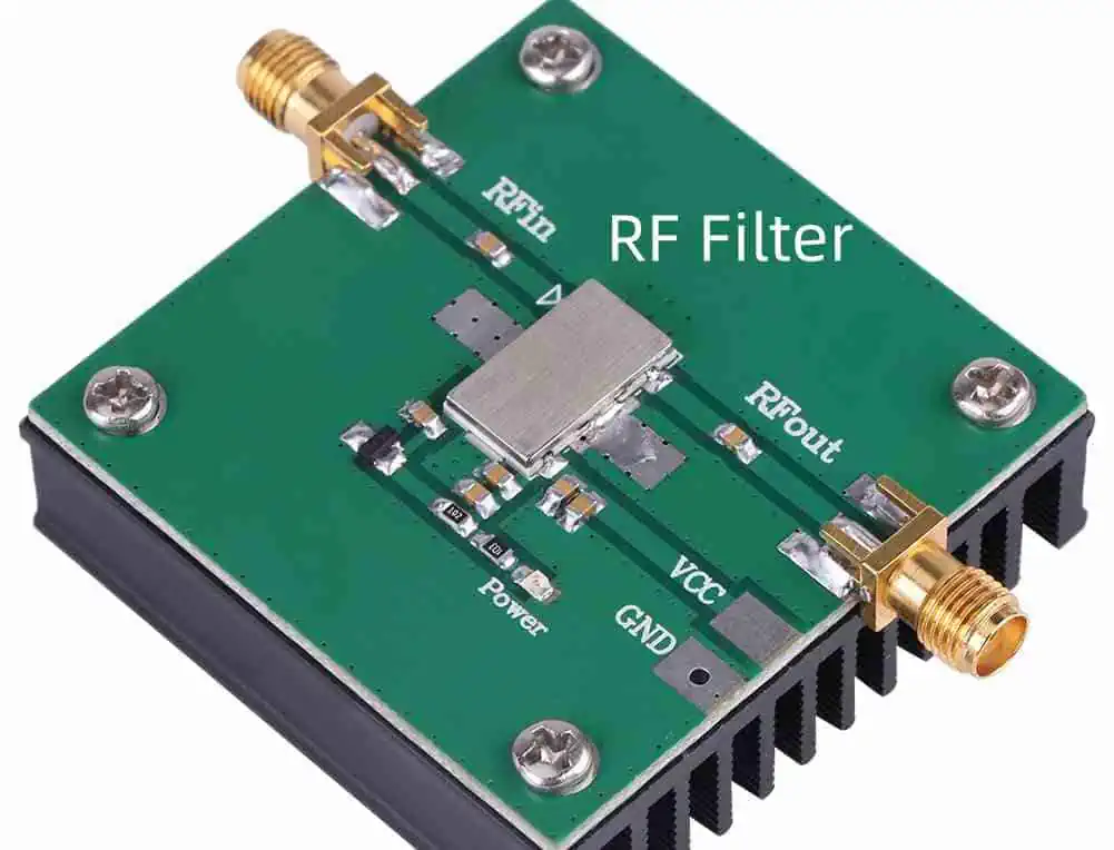
LC filters excel in high-frequency and high-power applications because:

  • Lower power loss compared to RC filters
  • Steeper roll-off characteristics
  • Better performance at radio frequencies
  • Can handle higher power levels
  • Higher Q-factor (quality factor)

Example Schematic

A basic LC low pass filter might look like:

Input ---[Inductor]---+---Output
                      |
                  [Capacitor]
                      |
                     GND

The cutoff frequency for this filter is given by: fc = 1/(2π√(LC))

Applications

LC filters are commonly found in:

  • RF and microwave systems
  • Power line filtering
  • High-efficiency power supplies
  • Antenna matching networks
  • Audio crossover networks for speakers

6. RL (Resistor-Inductor) Low Pass Filter

RL filters use the frequency-dependent properties of inductors combined with resistors to create a low pass filter.

Basic Operation

In an RL low pass filter:

  • The inductor is placed in series with the signal path
  • The resistor is typically the load resistance or a parallel resistor
  • Low frequencies encounter minimal opposition from the inductor
  • High frequencies face increasing opposition from the inductor

Applications in Power Systems

RL filters are particularly useful in:

  • Motor control circuits
  • Power line conditioning
  • Inductive load driving
  • DC power supplies
  • Current smoothing applications

Applications of Low Pass Filters

RF Filters
RF Filters

Low pass filters are ubiquitous in electronic systems, playing crucial roles across numerous fields and applications. Understanding these applications provides insight into the versatility and importance of these fundamental components.

Audio Processing

In audio systems, low pass filters serve multiple essential functions:

Speaker Crossover Networks: Low pass filters direct only the low-frequency components to subwoofers and bass speakers, ensuring each speaker reproduces only the frequencies it’s designed to handle efficiently. This improves sound quality and protects speakers from damage.

Audio Equalization: Low pass filters form the foundation of equalizers, allowing sound engineers and audiophiles to shape frequency response for optimal sound reproduction or creative effects.

Subwoofer Integration: Dedicated low pass filters ensure that subwoofers receive only low-frequency content, typically below 80-120Hz, optimizing bass reproduction in home theater and professional audio systems.

Noise Reduction: By filtering out high-frequency noise while preserving the audio spectrum, low pass filters can improve signal-to-noise ratio in recording and playback systems.

Radio Communications

Communication systems rely heavily on low pass filtering:

Channel Filtering: Low pass filters isolate specific frequency bands, helping receivers extract desired signals from crowded radio spectrums.

Bandwidth Limitation: Regulatory requirements often specify maximum bandwidths for transmissions; low pass filters ensure compliance by restricting the spectrum of transmitted signals.

Intermediate Frequency (IF) Processing: In superheterodyne receivers, low pass filters help process intermediate frequency signals before final demodulation.

Signal Demodulation: Many demodulation schemes require low pass filtering to extract the original information signal from the carrier wave.

Power Supplies and Noise Reduction

Power supply design frequently incorporates low pass filters:

Ripple Reduction: Low pass filters smooth the rectified AC in power supplies, reducing ripple voltage and providing cleaner DC output.

EMI/RFI Suppression: Filters prevent high-frequency noise from entering sensitive circuits or radiating from power lines, helping devices meet electromagnetic compatibility (EMC) requirements.

Power Line Conditioning: Low pass filters block high-frequency noise on power lines, protecting sensitive equipment and improving performance.

Transient Suppression: By attenuating high-frequency components, properly designed filters can help mitigate the effects of voltage spikes and transients.

Digital Signal Smoothing

In digital systems, low pass filtering plays a key role:

Anti-Aliasing: Before analog-to-digital conversion, low pass filters restrict the signal bandwidth to prevent aliasing artifacts.

Data Smoothing: Digital low pass filters can reduce noise and extract trends from noisy data streams, valuable in applications from weather prediction to stock market analysis.

Sensor Signal Conditioning: Low pass filters remove high-frequency noise from sensor outputs, producing cleaner signals for processing.

Image Processing: In digital image manipulation, low pass filtering produces blurring effects and removes high-frequency noise, useful for preprocessing in computer vision applications.

Biomedical Engineering

Medical devices rely extensively on low pass filtering:

ECG Signal Processing: Low pass filters remove high-frequency interference while preserving the critical cardiac waveform information.

EEG Monitoring: Brain activity monitoring systems use low pass filters to isolate specific frequency bands of interest.

Medical Imaging: MRI, ultrasound, and other imaging technologies employ sophisticated filtering to enhance image quality and diagnostic value.

Patient Monitoring: Vital signs monitors use low pass filters to stabilize readings and reduce false alarms from transient noise.

Everyday Examples

Low pass filters are present in many everyday consumer devices:

Smartphone Touchscreens: Low pass filtering algorithms help distinguish intentional touches from inadvertent contact or electrical noise.

Camera Stabilization: Digital cameras use low pass filtering to smooth out handheld camera movements.

Home Wi-Fi Routers: RF sections employ low pass filters to ensure transmissions remain within allocated frequency bands.

Automotive Electronics: From engine control modules to infotainment systems, vehicles use numerous low pass filters for signal conditioning and noise reduction.

Read more about:

Design Guide for Low Pass Filters

RF Filter PCB
RF Filter PCB

Creating an effective low pass filter requires careful planning and consideration of multiple factors. This step-by-step guide will help you design filters that meet your specific requirements.

1. Define Requirements

Before selecting components or drawing schematics, clearly establish what you need from your filter:

Cutoff Frequency

Determine the precise frequency boundary between signals you want to keep and those you want to attenuate. Consider:

  • The highest frequency component in your desired signal
  • The lowest frequency component you need to reject
  • Any transition band requirements

Desired Roll-off Rate

Decide how rapidly the filter should attenuate signals above the cutoff frequency:

  • Gentle roll-off (20 dB/decade): First-order filter, simpler but less effective
  • Moderate roll-off (40 dB/decade): Second-order filter, good compromise
  • Steep roll-off (60+ dB/decade): Higher-order filters, more complex but more effective

Passband and Stopband Specifications

Define the acceptable variation in your filter’s response:

  • Passband ripple: Maximum allowable amplitude variation for frequencies you want to pass
  • Stopband attenuation: Minimum required attenuation for frequencies you want to reject
  • Transition band width: How quickly the filter transitions from pass to reject

2. Choose Filter Type

Based on your requirements, select the most appropriate filter category:

Analog vs. Digital

Consider:

  • Operating environment (analog or digital domain)
  • Available processing resources
  • Required precision and flexibility
  • Budget constraints

Active vs. Passive

Consider:

  • Power availability
  • Required gain
  • Circuit complexity
  • Noise sensitivity
  • Available space

Filter Response Type

Different mathematical models offer different performance characteristics:

  • Butterworth: Maximally flat passband, moderate roll-off
  • Chebyshev: Steeper roll-off with some passband ripple
  • Bessel: Linear phase response, minimal signal distortion
  • Elliptic (Cauer): Sharpest transition but ripple in both passband and stopband

3. Select Components

Once you’ve decided on the filter type, select appropriate components:

How to Choose Capacitors

Consider these factors:

  • Tolerance: Precision applications require tighter tolerances (±1% or better)
  • Temperature coefficient: Choose stable types like NP0/C0G for critical applications
  • Voltage rating: Should exceed maximum expected voltage by at least 2x
  • ESR and ESL: Lower values improve high-frequency performance
  • Dielectric: Different types (ceramic, film, electrolytic) suit different applications

Selecting Inductors

For LC filters, inductor selection is critical:

  • Current rating: Must exceed maximum expected current
  • DCR (DC resistance): Lower values reduce power loss
  • Core material: Affects frequency response, saturation, and losses
  • Shielding: May be necessary to prevent EMI issues
  • Q factor: Higher values provide sharper resonance

Resistor Considerations

For RC and active filters:

  • Power rating: Ensure adequate heat dissipation
  • Noise characteristics: Critical in low-level signal processing
  • Tolerance: Affects filter accuracy
  • Temperature coefficient: Important for stable operation across temperatures
  • Type: Thick film, thin film, wirewound, etc., each with different characteristics

Tolerances and Practical Tips

Real-world components differ from ideal:

  • Use Monte Carlo analysis to evaluate the effect of component tolerances
  • Consider using 1% or better tolerance components for critical filters
  • Design with slightly adjusted values to accommodate standard component values
  • For stringent requirements, consider tunable components
  • Remember that capacitor values often drift with age and temperature

4. Simulate and Test

Before finalizing your design, verify its performance:

Tools for Simulation

Modern software makes filter design and verification accessible:

  • LTspice: Free SPICE simulator excellent for analog filter design
  • MATLAB/Simulink: Powerful platform for both analog and digital filter design
  • FilterLab: Specialized for active filter design
  • Python with SciPy: Excellent for digital filter prototyping
  • Online calculators: Quick checks for simple filters

Importance of Testing Before Implementation

Simulation can reveal issues before you build:

  • Verify actual cutoff frequency and roll-off
  • Check for unexpected resonances or anomalies
  • Assess sensitivity to component variations
  • Verify phase response if timing is critical
  • Estimate power consumption and thermal behavior

If possible, breadboard your design and test with real signals before final implementation.

5. Practical Design Tips

Theoretical design is just the beginning—practical implementation requires attention to detail:

Dealing with Parasitics

Real components have parasitic elements that can affect performance:

  • Keep leads short to minimize inductance
  • Consider capacitor ESR in high-frequency designs
  • Be aware of inter-winding capacitance in inductors
  • Use guard traces for sensitive nodes
  • Consider shielding for high-precision filters

PCB Layout Considerations

Circuit board layout significantly impacts filter performance:

  • Keep signal paths short and direct
  • Use ground planes for low impedance returns
  • Separate analog and digital grounds appropriately
  • Orient components to minimize coupling
  • Consider trace impedance at higher frequencies

Power Supply Decoupling

For active filters:

  • Use local decoupling capacitors near op-amp power pins
  • Employ multiple capacitor values for broadband decoupling
  • Consider using ferrite beads for additional filtering
  • Maintain low-impedance power supply paths
  • Isolate sensitive analog sections from digital noise

Common Mistakes in Low Pass Filter Design

Even experienced designers can fall into these common pitfalls. Being aware of them can save you time and frustration.

Incorrect Cutoff Frequency

A frequent error is misinterpreting or miscalculating the cutoff frequency:

  • Confusing -3dB point with other definitions of cutoff
  • Using incorrect formulas for different filter topologies
  • Failing to account for component tolerances
  • Not considering loading effects of connected circuits
  • Overlooking frequency shifts due to temperature variations

Overcomplicating the Design

Sometimes the simplest solution is the best:

  • Using higher-order filters when not necessary
  • Implementing active filters when passive would suffice
  • Adding unnecessary features that introduce potential failure points
  • Creating overly complex compensation networks
  • Choosing exotic filter responses without clear benefits

Ignoring Component Non-Idealities

Real components differ from their idealized models:

  • Capacitors have series resistance and inductance
  • Inductors have parallel capacitance and series resistance
  • Op-amps have limited bandwidth and slew rate
  • Resistors generate noise and have parasitic capacitance
  • All components have temperature coefficients and aging characteristics

Other Common Issues

Additional pitfalls to avoid:

  • Neglecting input/output impedance matching
  • Failing to consider the signal’s dynamic range
  • Ignoring phase response when it matters
  • Not validating designs with worst-case analysis
  • Overlooking power supply noise effects on active filters

Latest Trends and Innovations in Low Pass Filters (2025)

The field of filter design continues to evolve rapidly. These recent developments represent the cutting edge of filtering technology in 2025.

MEMS-Based Filters

Micro-Electro-Mechanical Systems (MEMS) technology has revolutionized filter design:

  • Microscopic mechanical resonators replace traditional LC components
  • Exceptional performance at high frequencies
  • Dramatically reduced size compared to conventional filters
  • Improved temperature stability
  • Integration with semiconductor manufacturing processes

These filters are increasingly found in wireless devices, offering superior performance while consuming less space and power than traditional designs.

AI-Enhanced Digital Filters

Artificial intelligence is transforming digital filter design and implementation:

  • Neural networks adaptively optimize filter coefficients
  • Machine learning algorithms predict and compensate for component aging
  • Self-tuning filters adjust their characteristics based on real-time signal analysis
  • AI-optimized filter architectures outperform traditionally designed filters
  • Reduced computational requirements through intelligent algorithm selection

These smart filters are particularly valuable in applications with varying signal characteristics or challenging noise environments.

Integrated Solutions in ICs

Modern integrated circuit technology incorporates increasingly sophisticated filtering capabilities:

  • Complete filter solutions in single-chip packages
  • Programmable analog filters with digital control
  • Switched-capacitor implementations with exceptional precision
  • Software-defined filtering architectures
  • Mixed-signal approaches combining the best of analog and digital techniques

These integrated solutions reduce component count, improve reliability, and lower system cost while offering performance that was previously unattainable.

Advanced Materials and Techniques

Novel materials and fabrication methods are expanding filter capabilities:

  • High-Q ceramic resonators for RF applications
  • Superconducting filters for quantum computing systems
  • Metamaterial structures creating previously impossible frequency responses
  • Carbon nanotube-based components with exceptional performance
  • 3D-printed RF structures for custom filter responses

These advances particularly benefit specialized applications with extreme requirements for selectivity, power handling, or size constraints.

Conclusion

Low pass filters represent one of the fundamental building blocks of electronic systems, performing the crucial task of separating wanted signals from unwanted ones based on frequency content. From the simplest RC network to sophisticated digital implementations, these filters enable countless technologies that we rely on daily. As we’ve explored in this guide, low pass filters come in many forms, each with distinct advantages and ideal applications.

When designing or selecting a low pass filter, remember to clearly define your requirements first, then choose the appropriate filter type and topology that best matches those needs. Pay close attention to component selection, and always verify your design through simulation and testing before final implementation. By avoiding common pitfalls and staying aware of the latest developments in filter technology, you can create efficient, effective filtering solutions for even the most demanding applications.

As technology continues to advance, we can expect even more innovative approaches to filtering, with improvements in size, performance, and integration. However, the fundamental principles of low pass filtering will remain essential knowledge for anyone working with electronic systems and signal processing.

FAQs About Low Pass Filters

What is the best low pass filter for audio applications?

The “best” filter depends on your specific requirements, but Butterworth filters are often preferred for audio because they provide maximally flat frequency response in the passband, avoiding coloration of the audio. For crossovers, Linkwitz-Riley filters (which are cascaded Butterworth filters) are popular because they provide -6dB response at the crossover point when summed with their high-pass counterparts. For applications where phase response is critical, Bessel filters may be preferred due to their linear phase characteristics, which preserve the waveform shape.

Can I use a low pass filter for DC signals?

Yes, low pass filters work perfectly with DC signals since DC is essentially a signal with zero frequency, which falls well within the passband of any low pass filter. In fact, one common application of low pass filters is extracting the DC component from a mixed signal. However, if your signal is purely DC with no AC components, a filter wouldn’t be necessary unless you’re trying to remove noise or ripple.

How do I calculate the cutoff frequency?

The formula depends on the filter type:

  • For RC filters: fc = 1/(2πRC)
  • For RL filters: fc = R/(2πL)
  • For LC filters: fc = 1/(2π√(LC))
  • For active filters: depends on the specific topology, but many follow the RC formula

Where:

  • fc is the cutoff frequency in Hz
  • R is resistance in ohms
  • C is capacitance in farads
  • L is inductance in henries

Online calculators and design tools can simplify these calculations for more complex filter types.

Passive vs. active low pass filter: which is better?

Neither is inherently “better” as each has advantages for different situations:

Choose passive filters when:

  • No power source is available
  • Simplicity is paramount
  • Working with high power levels
  • High reliability is essential
  • Working at very high frequencies

Choose active filters when:

  • Signal amplification is needed
  • Precise filter characteristics are required
  • Multiple filter stages must be cascaded
  • Input/output impedance matching is important
  • Working with very low frequencies

For many modern applications, active filters are preferred due to their flexibility and performance, but passive filters remain important in power electronics, RF design, and other specialized fields.

How do I design a low pass filter for a specific application?

Start by defining your requirements precisely:

  1. Determine the required cutoff frequency
  2. Identify necessary attenuation rate (roll-off)
  3. Consider any phase response requirements
  4. Define acceptable passband ripple
  5. Consider physical constraints (size, cost, power)

Then: 6. Select an appropriate filter topology 7. Calculate component values using formulas or design tools 8. Choose actual components considering tolerances and non-idealities 9. Simulate your design with realistic component models 10. Build and test a prototype before final implementation

For complex filters, specialized design software can greatly simplify this process.

ESP32-WROOM vs. ESP32-C3: Key Differences and Best Use Cases

Introduction

The world of Internet of Things (IoT) and embedded systems is evolving rapidly, with new microcontrollers and System-on-Chip (SoC) solutions emerging to meet diverse project requirements. Among the popular choices for developers and engineers are the ESP32 series modules from Espressif Systems. Two notable contenders in this series are the ESP32-WROOM and the ESP32-C3. This comprehensive comparison will delve into the key differences between these modules, helping you make an informed decision for your next project.

In this article, we’ll explore the unique features, capabilities, and best use cases for both the ESP32-WROOM and ESP32-C3. By the end, you’ll have a clear understanding of which module is best suited for your specific needs, whether you’re working on a high-performance IoT application, a low-power device, or a cost-sensitive project.

YouTube video

Overview of Each Module

ESP32-WROOM

General Description

The ESP32-WROOM is a powerful and versatile module that has become a staple in many IoT and embedded projects. It’s known for its robust performance, extensive feature set, and wide range of capabilities.

Key Specifications

  • Processor: Dual-core Tensilica Xtensa LX6 microprocessor
  • Clock Speed: Up to 240 MHz
  • Memory: 520 KB SRAM, 448 KB ROM
  • Flash: 4 MB external flash
  • Wireless Connectivity: Wi-Fi 802.11 b/g/n (2.4 GHz) and Bluetooth 4.2 (Classic and BLE)
  • GPIO: Up to 34 programmable GPIOs

Typical Applications

  • Smart home devices
  • Industrial automation
  • Wearable electronics
  • Audio processing applications
  • Wireless cameras and video streaming
  • Complex IoT systems requiring significant processing power

ESP32-C3

General Description

The ESP32-C3 is a more recent addition to the ESP32 family, designed with a focus on cost-effectiveness, power efficiency, and enhanced security features. It aims to provide a balance between performance and energy consumption.

Key Specifications

  • Processor: Single-core 32-bit RISC-V microprocessor
  • Clock Speed: Up to 160 MHz
  • Memory: 400 KB SRAM, 384 KB ROM
  • Flash: 4 MB external flash
  • Wireless Connectivity: Wi-Fi 802.11 b/g/n (2.4 GHz) and Bluetooth 5.0
  • GPIO: Up to 22 programmable GPIOs

Typical Applications

Key Differences

1. Processor and Architecture

One of the most significant differences between the ESP32-WROOM and ESP32-C3 lies in their processor architecture.

ESP32-WROOM: Dual-core Tensilica Xtensa

The ESP32-WROOM features a dual-core Tensilica Xtensa LX6 microprocessor. This architecture provides:

  • Two high-performance cores capable of running at up to 240 MHz
  • Ability to handle complex tasks and multitasking efficiently
  • Support for floating-point and double-precision operations

ESP32-C3: Single-core RISC-V

In contrast, the ESP32-C3 employs a single-core 32-bit RISC-V microprocessor:

  • Runs at up to 160 MHz
  • RISC-V architecture offers better code density and power efficiency
  • Simpler architecture, potentially easier for optimization

Performance Implications

The dual-core nature of the ESP32-WROOM makes it superior for applications requiring intensive processing or multitasking. It excels in scenarios like:

  • Real-time audio or video processing
  • Running complex algorithms alongside wireless communication tasks
  • Handling multiple sensors and actuators simultaneously

The ESP32-C3, while less powerful in raw processing capability, offers advantages in:

  • Power efficiency, making it suitable for battery-operated devices
  • Cost-effectiveness for simpler IoT applications
  • Potentially easier development process due to the open-source RISC-V architecture

2. Wireless Connectivity

Both modules offer robust wireless connectivity options, but there are some key differences to consider.

Wi-Fi Capabilities

Both the ESP32-WROOM and ESP32-C3 support Wi-Fi 802.11 b/g/n in the 2.4 GHz band. This means they can easily connect to most modern Wi-Fi networks and serve as access points when needed.

Bluetooth Differences

  • ESP32-WROOM: Supports Bluetooth 4.2, including both Classic Bluetooth and Bluetooth Low Energy (BLE)
  • ESP32-C3: Features Bluetooth 5.0, focusing on BLE with enhanced features

The ESP32-C3’s Bluetooth 5.0 support brings several advantages:

  • Longer range (up to 4x compared to Bluetooth 4.2)
  • Higher data transfer speeds (up to 2x)
  • Improved coexistence with other wireless technologies
  • Support for Bluetooth mesh networking

These improvements make the ESP32-C3 particularly suitable for IoT applications requiring extended Bluetooth range or more efficient data transfer.

3. Security Features

In today’s interconnected world, security is paramount. Both modules offer security features, but the ESP32-C3 takes it a step further.

ESP32-C3: Advanced Security

The ESP32-C3 boasts enhanced security features:

  • Hardware-accelerated encryption (AES, SHA, RSA, ECC)
  • Secure boot ensures only authenticated firmware can run
  • Flash encryption protects sensitive data and code
  • Digital signature peripheral for faster and more secure operations

ESP32-WROOM: Solid Security Basics

While not as advanced as the C3, the ESP32-WROOM still offers robust security:

  • Hardware encryption acceleration
  • Secure boot capability
  • Flash encryption

The additional security features of the ESP32-C3 make it an excellent choice for applications where data protection is critical, such as smart locks, industrial sensors, or any device handling sensitive information.

4. Power Consumption

Power efficiency is a crucial factor, especially for battery-operated devices. Here’s how the two modules compare:

ESP32-WROOM Power Profile

  • Generally higher power consumption due to dual-core architecture
  • More versatile power modes, including deep sleep
  • Typical power consumption in active mode: 80mA

ESP32-C3 Power Efficiency

  • Designed with low power consumption as a priority
  • Efficient single-core RISC-V architecture
  • Typical power consumption in active mode: 60mA
  • Enhanced low-power modes for extended battery life

The ESP32-C3’s focus on power efficiency makes it the better choice for battery-powered applications or devices that need to operate for extended periods without recharging.

Read more about:

5. Peripheral Support

Both modules offer a wide range of peripherals, but there are some differences to note:

ESP32-WROOM Peripherals

  • Up to 34 programmable GPIOs
  • 16 channels of 12-bit ADC
  • 2 channels of 8-bit DAC
  • 16 channels of PWM
  • 4 SPI interfaces
  • 2 I2S interfaces
  • 3 UART interfaces

ESP32-C3 Peripherals

  • Up to 22 programmable GPIOs
  • 6 channels of 12-bit ADC
  • 6 channels of PWM
  • 3 SPI interfaces
  • 1 I2S interface
  • 2 UART interfaces

The ESP32-WROOM offers more flexibility with its higher number of GPIOs and additional peripherals, making it suitable for more complex projects requiring numerous inputs and outputs. The ESP32-C3, while having fewer peripherals, still provides ample options for most IoT applications.

6. Development Environment and Ecosystem

Both modules benefit from Espressif’s robust development ecosystem, but there are some differences to consider:

ESP32-WROOM Development

  • Well-established ecosystem with extensive community support
  • Compatible with ESP-IDF (Espressif IoT Development Framework)
  • Supported by popular platforms like Arduino IDE
  • Vast number of libraries and example projects available

ESP32-C3 Development

  • Growing ecosystem with increasing community support
  • Also compatible with ESP-IDF
  • Supports Arduino IDE, but may require additional setup
  • RISC-V architecture may require different toolchains and compilation process

While both modules can be programmed using similar tools, developers familiar with the ESP32-WROOM might face a slight learning curve when switching to the ESP32-C3 due to its RISC-V architecture. However, Espressif has made efforts to ensure a smooth transition between the two platforms.

7. Price and Availability

Price and availability can be significant factors in choosing between these modules:

ESP32-WROOM

  • Generally more expensive due to its dual-core architecture and higher performance
  • Widely available from numerous suppliers
  • Price range: 3to3to6 per unit (varies based on quantity and supplier)

ESP32-C3

  • Designed as a cost-effective alternative
  • Becoming increasingly available as adoption grows
  • Price range: 2to2to4 per unit (varies based on quantity and supplier)

The ESP32-C3’s lower price point makes it an attractive option for cost-sensitive projects or large-scale deployments where even small price differences can have a significant impact.

Best Use Cases

When to Choose ESP32-WROOM

The ESP32-WROOM is ideal for:

  1. High-performance IoT applications: When you need significant processing power for complex tasks or real-time operations.
  2. Multimedia projects: For applications involving audio processing, camera interfacing, or video streaming.
  3. Multi-tasking scenarios: When your project requires running multiple operations simultaneously, leveraging the dual-core architecture.
  4. Projects with numerous peripherals: If you need a large number of GPIOs or specific peripheral interfaces not available on the C3.
  5. Prototype development: When you’re in the early stages and want maximum flexibility and processing power to experiment with different features.

When to Choose ESP32-C3

The ESP32-C3 is best suited for:

  1. Low-power IoT devices: For battery-operated sensors or devices that need to run for extended periods without recharging.
  2. Secure IoT applications: When enhanced security features are crucial, such as in smart locks, industrial sensors, or devices handling sensitive data.
  3. Cost-sensitive projects: For large-scale deployments or products where minimizing unit cost is essential.
  4. Simple, smaller-footprint designs: When your project doesn’t require the full power of a dual-core processor and can benefit from a more streamlined design.
  5. Bluetooth 5.0 specific applications: If you need the extended range, higher speed, or mesh networking capabilities of Bluetooth 5.0.

Comparison Table

Here’s a side-by-side comparison of the key specifications:

FeatureESP32-WROOMESP32-C3
ProcessorDual-core Tensilica XtensaSingle-core RISC-V
Clock SpeedUp to 240 MHzUp to 160 MHz
SRAM520 KB400 KB
ROM448 KB384 KB
Flash4 MB (external)4 MB (external)
Wi-Fi802.11 b/g/n (2.4 GHz)802.11 b/g/n (2.4 GHz)
Bluetooth4.2 (Classic and BLE)5.0
GPIOUp to 34Up to 22
ADC16 channels, 12-bit6 channels, 12-bit
Security FeaturesBasic (secure boot, encryption)Advanced (additional hardware security)
Power ConsumptionHigherLower
Price Range3−3−62−2−4

Conclusion

Choosing between the ESP32-WROOM and ESP32-C3 ultimately depends on your project’s specific requirements. Both modules offer impressive capabilities and are part of a robust ecosystem supported by Espressif Systems.

The ESP32-WROOM remains the go-to choice for projects requiring high performance, extensive peripheral support, or complex multitasking. Its dual-core architecture and wealth of features make it ideal for sophisticated IoT applications, multimedia projects, and scenarios where processing power is paramount.

On the other hand, the ESP32-C3 shines in situations where power efficiency, enhanced security, and cost-effectiveness are primary concerns. Its RISC-V architecture, Bluetooth 5.0 support, and advanced security features make it an excellent choice for modern IoT devices, especially those that are battery-powered or require robust data protection.

When making your decision, consider factors such as:

  1. Processing requirements
  2. Power constraints
  3. Security needs
  4. Peripheral requirements
  5. Project budget
  6. Development timeline and team expertise

By carefully evaluating these aspects against the strengths of each module, you can select the option that best aligns with your project goals. Whether you opt for the versatile powerhouse that is the ESP32-WROOM or the efficient and secure ESP32-C3, you’ll be working with a capable platform backed by a strong community and extensive resources.

As the IoT landscape continues to evolve, both these modules offer compelling solutions for a wide range of applications. By understanding their key differences and best use cases, you’re now equipped to make an informed decision that will set your project up for success.

High Power LED Lights with 100W, 200W, and Higher Power

High power LED lights have revolutionized the lighting industry, offering unprecedented levels of brightness, energy efficiency, and durability. As technology advances, we’re seeing more powerful LEDs hitting the market, with 100W, 200W, and even higher wattage options becoming increasingly common. This article will explore the world of high power LED lights, their applications, benefits, challenges, and future prospects.

YouTube video

Understanding High Power LED Lights

What Are High Power LED Lights?

High power LED lights are lighting solutions that use light-emitting diodes (LEDs) capable of producing extremely high levels of illumination. These LEDs are designed to handle significantly more electrical power than standard LEDs, resulting in much higher light output.

Key Characteristics of High Power LEDs

  1. High Lumen Output: Capable of producing thousands of lumens per LED package.
  2. Improved Efficacy: Higher lumens per watt compared to traditional lighting sources.
  3. Thermal Management: Requires advanced heat dissipation techniques.
  4. Longevity: Long lifespan, often rated for 50,000 hours or more.
  5. Compact Size: High light output from a relatively small form factor.

Applications of High Power LED Lights

Industrial Lighting

  1. Warehouses: High bay lighting for large storage facilities.
  2. Manufacturing Plants: Bright, uniform lighting for production lines and work areas.
  3. Mining: Durable, high-intensity lighting for underground and surface operations.

Outdoor Lighting

  1. Street Lighting: Energy-efficient illumination for roads and highways.
  2. Sports Facilities: High-intensity lighting for stadiums and outdoor courts.
  3. Architectural Lighting: Dramatic illumination of buildings and landscapes.

Commercial Lighting

  1. Retail Spaces: Bright, attractive lighting for showrooms and display areas.
  2. Convention Centers: Flexible, high-output lighting for various events.
  3. Theaters and Studios: Powerful, controllable lighting for stage and film production.

Specialty Applications

  1. Horticulture: High-intensity grow lights for indoor farming.
  2. Automotive: High-power headlights and auxiliary lighting.
  3. Marine: Durable, high-output lighting for ships and offshore structures.

Comparison of 100W, 200W, and Higher Power LED Lights

Parameter100W LED200W LED300W+ LED
Lumen Output (approx.)10,000-15,000 lm20,000-30,000 lm30,000-45,000+ lm
Efficacy (lm/W)100-150100-150100-150
Heat GenerationModerateHighVery High
Typical ApplicationsSmall warehouses, Street lightingLarge warehouses, Sports lightingStadiums, Large outdoor areas
Initial CostModerateHighVery High
Energy Savings vs. HID60-70%60-70%60-70%
Lifespan (hours)50,000-100,00050,000-100,00050,000-100,000
Color Rendering Index70-95+70-95+70-95+
Beam Angle Options60°-120°60°-120°60°-120°

Technology Behind High Power LED Lights

LED Chip Design

  1. Chip-on-Board (COB) Technology: Multiple LED chips are packaged together to form a single, high-output light source.
  2. Multi-Die Arrays: Several high-power LED dies are combined in a single package.
  3. Advanced Semiconductor Materials: Use of materials like Gallium Nitride (GaN) for improved efficiency and heat tolerance.

Thermal Management

  1. Heat Sinks: Large, often finned aluminum structures to dissipate heat.
  2. Active Cooling: Fans or liquid cooling systems for extremely high-power applications.
  3. Thermal Interface Materials: Specialized materials to improve heat transfer from LED to heat sink.

Power Supply and Drivers

  1. Constant Current Drivers: Ensure stable current supply to maintain consistent light output and protect LEDs.
  2. High Efficiency Power Supplies: Minimize energy loss in power conversion.
  3. Intelligent Control Systems: Allow for dimming, color tuning, and integration with smart lighting systems.

Optics and Light Distribution

  1. Reflectors: Shaped reflective surfaces to control beam angle and light distribution.
  2. Lenses: Precision-engineered lenses to focus or diffuse light as needed.
  3. Total Internal Reflection (TIR) Optics: Advanced optical systems for precise light control.

Benefits of High Power LED Lights

Energy Efficiency

High power LED lights offer significant energy savings compared to traditional high-intensity discharge (HID) lamps. They can provide the same or higher light output while consuming up to 70% less energy.

Long Lifespan

With proper thermal management, high power LEDs can last 50,000 to 100,000 hours or more, significantly reducing maintenance and replacement costs.

Improved Light Quality

Modern high power LEDs offer excellent color rendering (CRI 70-95+) and a wide range of color temperatures, providing high-quality light for various applications.

Instant On/Off

Unlike HID lamps, high power LEDs reach full brightness instantly and can be switched on and off rapidly without affecting lifespan.

Directional Light Output

LEDs emit light in a specific direction, reducing the need for reflectors and diffusers, which can trap light.

Environmental Benefits

LED lights contain no mercury and produce less waste due to their long lifespan, making them a more environmentally friendly option.

Challenges and Considerations

Heat Management

As LED power increases, managing heat becomes increasingly critical. Proper thermal design is essential to maintain performance and longevity.

Initial Cost

High power LED lights often have a higher upfront cost compared to traditional lighting solutions, although this is often offset by long-term energy savings and reduced maintenance.

Light Distribution

Achieving uniform light distribution over large areas can be challenging with very high-power LEDs and may require careful optical design.

Power Supply Reliability

The performance and lifespan of high power LED systems are heavily dependent on the quality and reliability of their power supplies and drivers.

Glare and Light Pollution

The intense brightness of high power LEDs can cause glare issues if not properly managed, potentially contributing to light pollution in outdoor applications.

Future Trends in High Power LED Lighting

Increased Efficiency

Ongoing research aims to push LED efficacy even higher, potentially reaching 200 lumens per watt or more in commercial products.

Advanced Materials

Development of new semiconductor materials and phosphors to improve performance and expand the range of available spectra.

Smart Integration

Integration of high power LEDs with advanced control systems, sensors, and IoT technologies for improved energy management and customization.

Miniaturization

Efforts to reduce the size of high power LED packages while maintaining or improving output and thermal performance.

Specialized Spectra

Development of LEDs with spectra tailored for specific applications, such as horticulture, human-centric lighting, and wildlife-friendly outdoor lighting.

Choosing the Right High Power LED Light

Factors to Consider

  1. Application Requirements: Determine the required light output, distribution pattern, and color characteristics.
  2. Environmental Conditions: Consider temperature, humidity, and potential exposure to dust or water.
  3. Energy Efficiency Goals: Calculate potential energy savings and return on investment.
  4. Maintenance Considerations: Evaluate accessibility and frequency of required maintenance.
  5. Control Requirements: Assess needs for dimming, color tuning, or integration with building management systems.
  6. Regulatory Compliance: Ensure the chosen solution meets relevant safety and performance standards.

Comparison of High Power LED Fixtures for Industrial Applications

Feature100W Fixture200W Fixture300W Fixture
Lumen Output13,000 lm26,000 lm39,000 lm
Efficacy130 lm/W130 lm/W130 lm/W
Color Temperature Options3000K, 4000K, 5000K3000K, 4000K, 5000K3000K, 4000K, 5000K
Beam Angle Options60°, 90°, 120°60°, 90°, 120°60°, 90°, 120°
Weight3.5 kg5.2 kg7.8 kg
Dimensions (LxWxH)300x250x100 mm400x300x120 mm500x350x140 mm
IP RatingIP65IP65IP65
Lifespan (L70)100,000 hours100,000 hours100,000 hours
Warranty5 years5 years5 years
Typical Mounting Height4-6 m6-9 m9-12 m
Recommended Coverage Area100-150 m²200-300 m²300-450 m²

Installation and Maintenance Best Practices

Installation Tips

  1. Proper Mounting: Ensure fixtures are securely mounted and properly aligned.
  2. Adequate Ventilation: Allow for sufficient airflow around fixtures to aid heat dissipation.
  3. Correct Wiring: Use appropriate gauge wires and ensure all connections are secure and properly insulated.
  4. Surge Protection: Install surge protection devices to guard against voltage spikes.
  5. Proper Aiming: Adjust fixture angles to minimize glare and optimize light distribution.

Maintenance Recommendations

  1. Regular Cleaning: Keep fixtures clean to maintain optimal light output and heat dissipation.
  2. Inspection Schedule: Regularly inspect fixtures for signs of damage or degradation.
  3. Driver Maintenance: Monitor and replace drivers as needed, as they often have a shorter lifespan than the LEDs themselves.
  4. Thermal Management Check: Periodically inspect heat sinks and cooling systems for proper operation.
  5. Light Level Monitoring: Use light meters to track output over time and plan for replacements.

Conclusion

High power LED lights with 100W, 200W, and higher wattages represent the cutting edge of lighting technology. They offer unprecedented levels of brightness, efficiency, and versatility, making them suitable for a wide range of demanding applications. While challenges such as heat management and initial cost remain, ongoing technological advancements continue to improve performance and reduce barriers to adoption. As the technology matures, we can expect to see even more powerful and efficient LED lighting solutions, further transforming how we illuminate our world.

Frequently Asked Questions (FAQ)

1. How do high power LED lights compare to traditional HID lamps in terms of energy efficiency?

High power LED lights are significantly more energy-efficient than traditional HID (High-Intensity Discharge) lamps. On average, LED lights can provide the same or higher light output while consuming 60-70% less energy. This efficiency translates to substantial energy savings over the lifetime of the fixture. For example, a 200W LED light might replace a 400W or 600W HID lamp, depending on the specific application and light requirements.

The higher efficiency of LEDs is due to several factors:

  1. LEDs convert a higher percentage of electrical energy directly into light, with less energy lost as heat.
  2. LED light is more directional, reducing the need for reflectors that can trap light.
  3. LED efficacy (lumens per watt) continues to improve with technological advancements.

It’s important to note that the exact energy savings can vary depending on the specific products being compared and the application requirements.

2. What are the main challenges in thermal management for high power LED lights?

Thermal management is one of the most critical challenges in high power LED lighting. As the power of LEDs increases, so does the amount of heat generated. Effective heat dissipation is crucial for maintaining LED performance and longevity. The main challenges include:

  1. Heat Concentration: High power LEDs produce a lot of heat in a small area, which can lead to hotspots.
  2. Temperature Sensitivity: LED performance and lifespan decrease as temperature increases.
  3. Limited Space: Many applications require compact designs, limiting options for heat sinks and cooling systems.
  4. Environmental Factors: Ambient temperature and airflow can significantly affect cooling efficiency.
  5. Material Limitations: Finding materials with high thermal conductivity that are also cost-effective and suitable for manufacturing.

To address these challenges, manufacturers employ various strategies:

  • Advanced heat sink designs with increased surface area
  • Use of high thermal conductivity materials like aluminum and copper
  • Integration of active cooling systems (fans or liquid cooling) for very high-power applications
  • Thermal simulation and testing to optimize designs
  • Use of thermally conductive interface materials to improve heat transfer from the LED to the heat sink

Proper thermal management is essential to ensure that high power LED lights achieve their rated lifespan and maintain consistent performance over time.

3. How long can I expect a high power LED light to last?

The lifespan of high power LED lights is typically much longer than traditional lighting sources. Most high-quality LED fixtures are rated for 50,000 to 100,000 hours of operation. However, it’s important to understand what this rating means:

  • LED lifespan is usually quoted as L70, which is the time it takes for the light output to decrease to 70% of its initial value.
  • This doesn’t mean the LED will completely fail at this point, but rather that its output has diminished to a level considered the end of its useful life for most applications.

Factors affecting LED lifespan include:

  1. Operating Temperature: Higher temperatures can significantly reduce lifespan.
  2. Drive Current: Running LEDs at higher currents can decrease lifespan.
  3. Thermal Management: Proper heat dissipation is crucial for longevity.
  4. Environmental Conditions: Exposure to humidity, vibration, and temperature fluctuations can impact lifespan.
  5. Quality of Components: The driver and other electronic components can fail before the LED itself.

In real-world applications, a high power LED light operated for 12 hours per day could potentially last over 11 years before reaching its L70 point. However, it’s important to note that other components in the fixture, particularly the driver, may need replacement before the LEDs themselves reach end-of-life.

Regular maintenance and proper installation in accordance with manufacturer specifications can help ensure that high power LED lights achieve or even exceed their rated lifespan.

4. Are high power LED lights suitable for outdoor use in extreme weather conditions?

Yes, high power LED lights can be designed for outdoor use in extreme weather conditions, but it’s crucial to choose fixtures specifically engineered for such environments. When selecting LED lights for challenging outdoor applications, consider the following factors:

  1. IP Rating: Look for fixtures with appropriate Ingress Protection (IP) ratings. For most outdoor applications, a minimum of IP65 is recommended, which provides protection against dust and water jets. For more extreme conditions, higher ratings like IP66 or IP67 may be necessary.
  2. Operating Temperature Range: Check the fixture’s specified operating temperature range. High-quality outdoor LED lights can often operate in temperatures from -40°C to +50°C or even wider ranges.
  3. Corrosion Resistance: For coastal or industrial areas, choose fixtures with corrosion-resistant materials and finishes, such as marine-grade aluminum or stainless steel.
  4. Wind Load Resistance: In areas prone to high winds, ensure the fixture and mounting system are designed to withstand expected wind loads.
  5. Thermal Management: Look for designs with effective passive cooling systems that can operate reliably without fans or other moving parts.
  6. Surge Protection: Outdoor fixtures should have robust surge protection to guard against lightning strikes and other electrical surges.
  7. UV Resistance: Ensure all external materials, including lenses and gaskets, are UV-resistant to prevent degradation from sun exposure.
  8. Vibration Resistance: For applications in areas with high vibration (e.g., bridges, industrial facilities), choose fixtures tested for vibration resistance.

Many manufacturers offer high power LED lights specifically designed for extreme environments, such as arctic regions, tropical climates, offshore installations, and high-altitude locations. These specialized fixtures often undergo rigorous testing to ensure reliability in challenging conditions.

Raspberry Pi 2 PiGRRL Pack 2.0 and Custom Gamepad PCB

The world of retro gaming has seen a resurgence in recent years, with enthusiasts seeking ways to relive their favorite classic games while leveraging modern technology. The Raspberry Pi 2 PiGRRL Pack 2.0, combined with a custom gamepad PCB, offers an exciting solution for DIY gaming enthusiasts. This article will explore the components, assembly process, and customization options for creating your own portable gaming device using the Raspberry Pi 2 PiGRRL Pack 2.0 and a custom gamepad PCB.

YouTube video

Understanding the Raspberry Pi 2 PiGRRL Pack 2.0

What is the PiGRRL Pack 2.0?

The PiGRRL Pack 2.0 is a comprehensive kit designed to transform a Raspberry Pi 2 into a portable gaming console. It builds upon the success of the original PiGRRL project, offering improved features and easier assembly.

Components of the PiGRRL Pack 2.0

The PiGRRL Pack 2.0 typically includes the following components:

| Component | Purpose | |———–|———| | 3D printed case | Houses all components | | 3.5″ TFT display | Serves as the game screen | | PowerBoost 1000C | Manages power and charging | | 2000mAh LiPo battery | Provides portable power | | Mini speaker | Outputs game audio | | Tactile buttons | Used for game controls | | Various wires and connectors | For internal connections |

Advantages of the PiGRRL Pack 2.0

  1. Compact design
  2. Improved battery life
  3. Better screen quality
  4. More ergonomic button layout
  5. Easier assembly process

The Custom Gamepad PCB

Why Use a Custom Gamepad PCB?

A custom gamepad PCB offers several advantages over traditional wiring methods:

  1. Cleaner internal layout
  2. Reduced wiring complexity
  3. Improved reliability
  4. Easier maintenance and troubleshooting
  5. Potential for additional features

Designing the Custom Gamepad PCB

Key Considerations

When designing a custom gamepad PCB for the PiGRRL Pack 2.0, consider the following:

  1. Button layout and ergonomics
  2. Compatibility with Raspberry Pi 2 GPIO pins
  3. Integration with PiGRRL Pack 2.0 components
  4. Potential for future upgrades or modifications

Essential Components

A typical custom gamepad PCB for the PiGRRL Pack 2.0 might include:

| Component | Purpose | |———–|———| | Microcontroller | Manages button inputs | | Tactile switches | Serve as game buttons | | Resistors | For button debouncing | | Connectors | Interface with Raspberry Pi and other components | | LED indicators | Provide visual feedback |

PCB Manufacturing Process

  1. Schematic design
  2. PCB layout
  3. Gerber file generation
  4. PCB fabrication
  5. Component sourcing
  6. PCB assembly

Assembling the Raspberry Pi 2 PiGRRL Pack 2.0 with Custom Gamepad PCB

Preparation

Before beginning the assembly process, ensure you have the following tools:

  1. Soldering iron and solder
  2. Wire strippers
  3. Screwdrivers
  4. Multimeter
  5. Heat shrink tubing
  6. Tweezers

Step-by-Step Assembly Guide

1. Prepare the 3D Printed Case

  • Clean up any 3D printing artifacts
  • Test-fit components to ensure proper alignment

2. Install the Display

  • Carefully mount the 3.5″ TFT display in the case
  • Secure with appropriate screws or mounting brackets

3. Prepare the Raspberry Pi 2

  • Install the required operating system (typically RetroPie)
  • Configure GPIO pins for gamepad input

4. Install the Custom Gamepad PCB

  • Mount the custom PCB in the designated area of the case
  • Connect to Raspberry Pi GPIO pins using appropriate cables

5. Power Management Setup

  • Install the PowerBoost 1000C
  • Connect the LiPo battery
  • Wire power to Raspberry Pi and display

6. Audio Installation

  • Mount the mini speaker
  • Connect audio output from Raspberry Pi

7. Final Assembly

  • Carefully route all wires
  • Secure components with screws or mounting brackets
  • Close up the case

Software Configuration

Operating System Setup

  1. Download and install RetroPie
  2. Configure RetroPie for the 3.5″ display
  3. Set up Wi-Fi (if applicable)

Gamepad Configuration

  1. Access RetroPie configuration menu
  2. Navigate to “Input” settings
  3. Follow on-screen instructions to map buttons

ROM Installation

  1. Prepare a list of legally owned game ROMs
  2. Transfer ROMs to Raspberry Pi using Wi-Fi or USB
  3. Organize ROMs into appropriate folders

Customization Options

Case Modifications

  • Custom paint jobs
  • Additional button holes
  • Improved ventilation

Hardware Upgrades

  • Larger battery for extended playtime
  • Improved audio amplifier for better sound
  • Bluetooth module for wireless controllers

Software Enhancements

  • Custom emulator configurations
  • Overclocking for improved performance
  • Customized boot screens and themes

Troubleshooting Common Issues

Display Problems

| Issue | Possible Solution | |——-|——————-| | No display output | Check connections, verify GPIO configuration | | Distorted image | Adjust display settings in config.txt | | Flickering screen | Ensure stable power supply |

Control Issues

| Issue | Possible Solution | |——-|——————-| | Unresponsive buttons | Verify PCB connections, check GPIO configuration | | Ghost inputs | Improve button debouncing in software or hardware | | Incorrect button mapping | Reconfigure input settings in RetroPie |

Power Problems

| Issue | Possible Solution | |——-|——————-| | Short battery life | Check for power-hungry processes, consider larger battery | | Failure to charge | Verify PowerBoost connections, check USB cable | | Sudden shutdowns | Ensure stable power supply, check for overheating |

Performance Optimization

Overclocking

  • Carefully adjust CPU and GPU clock speeds
  • Monitor temperatures to prevent overheating
  • Test stability with demanding games

Emulator-Specific Tweaks

  • Research optimal settings for each emulator
  • Balance performance and accuracy
  • Consider using lower resolution for smoother gameplay

System Optimization

  • Disable unnecessary services
  • Use lightweight themes
  • Regularly update software for bug fixes and improvements

Community and Resources

Online Forums

  • RetroPie forums
  • Raspberry Pi forums
  • 3D printing communities

Video Tutorials

  • YouTube channels dedicated to Raspberry Pi projects
  • Step-by-step assembly guides
  • Troubleshooting walkthroughs

Documentation

  • Official Raspberry Pi documentation
  • RetroPie wikis
  • Custom gamepad PCB design resources

Future Developments

Potential Upgrades

  • Integration with newer Raspberry Pi models
  • Support for more advanced displays
  • Improved power management systems

Emerging Technologies

  • Incorporation of mini HDMI for external display support
  • USB-C for faster charging and data transfer
  • Potential for cloud game streaming integration

Conclusion

The Raspberry Pi 2 PiGRRL Pack 2.0, combined with a custom gamepad PCB, offers an exciting platform for DIY gaming enthusiasts. By following the steps outlined in this article, you can create a unique, portable gaming device that blends retro charm with modern technology. The customization options and active community support ensure that your PiGRRL project can continue to evolve and improve over time.

Frequently Asked Questions (FAQ)

1. Can I use a different Raspberry Pi model with the PiGRRL Pack 2.0?

While the PiGRRL Pack 2.0 is designed specifically for the Raspberry Pi 2, it may be possible to use other models with some modifications. However, this could require changes to the case design, power management, and software configuration. It’s generally recommended to stick with the Raspberry Pi 2 for the best compatibility and performance with this particular pack.

2. How difficult is it to design and manufacture a custom gamepad PCB?

Designing and manufacturing a custom gamepad PCB requires some knowledge of electronics and PCB design. For beginners, it can be challenging, but there are many resources available online to help. You’ll need to learn how to use PCB design software, understand basic circuit design, and familiarize yourself with the PCB manufacturing process. Alternatively, you can start with existing open-source designs and modify them to suit your needs.

3. What’s the typical battery life of a completed PiGRRL 2.0 project?

The battery life of a PiGRRL 2.0 project can vary depending on several factors, including the efficiency of your components, the types of games you’re playing, and any additional features you’ve added. With the standard 2000mAh LiPo battery, you can typically expect 2-4 hours of gameplay. This can be extended by using a larger capacity battery or implementing more aggressive power-saving measures.

4. Can I add additional features like Wi-Fi or Bluetooth to my PiGRRL 2.0?

Yes, it’s possible to add features like Wi-Fi or Bluetooth to your PiGRRL 2.0 project. The Raspberry Pi 2 has built-in support for these technologies, so it’s mainly a matter of configuring the software and ensuring you have the necessary antennas or modules. Keep in mind that adding these features may impact battery life and could require modifications to the case design to accommodate any additional hardware.

5. Is it legal to play ROMs on the PiGRRL 2.0?

The legality of playing ROMs is a complex issue that varies by jurisdiction. Generally, it’s considered legal to play ROMs of games you own physical copies of, for personal use. However, downloading ROMs of games you don’t own is typically not legal. It’s important to research and comply with the copyright laws in your area. Many retro gaming enthusiasts choose to focus on open-source or homebrew games to avoid legal issues.

Laser Depaneling PCB: How to Depanelize Round Ceramic PCB

What is Laser Depaneling?

Laser depaneling is a cutting-edge technology that uses a focused laser beam to separate individual PCBs from a larger panel. This method offers numerous advantages over traditional mechanical depaneling techniques, especially when dealing with delicate or uniquely shaped PCBs like round ceramic boards.

The Science Behind Laser Depaneling

Laser depaneling works on the principle of material ablation. The laser beam, typically a CO2 or UV laser, is focused on the PCB material, vaporizing it along a predetermined path. This process creates a clean, precise cut without applying mechanical stress to the board.

YouTube video

Key Components of a Laser Depaneling System

  1. Laser Source
  2. Beam Delivery System
  3. Motion Control System
  4. Vision System
  5. Exhaust and Filtration System

Advantages of Laser Depaneling for Round Ceramic PCBs

  1. Precision: Laser cutting offers unparalleled accuracy, crucial for round shapes.
  2. Stress-Free: No mechanical stress is applied to the delicate ceramic material.
  3. Clean Cuts: Laser cutting produces smooth edges without debris.
  4. Flexibility: Easily adaptable for various board shapes and sizes.
  5. Programmability: Can be quickly reprogrammed for different designs.

Preparing for Laser Depaneling of Round Ceramic PCBs

Material Considerations

Ceramic PCBs have unique properties that make them ideal for certain applications but also require special handling during the depaneling process.

Properties of Ceramic PCBs

PropertyCharacteristicImplication for Depaneling
Thermal ConductivityHighRequires careful power adjustment
BrittlenessHighProne to chipping if mishandled
Dielectric ConstantHighExcellent for RF applications
Coefficient of Thermal ExpansionLowLess warping during laser cutting

Design Considerations for Laser Depaneling

When designing round ceramic PCBs for laser depaneling, several factors should be taken into account:

  1. Panel Layout
  2. Depaneling Path Design
  3. Tab Design (if applicable)
  4. Fiducial Marks for Alignment

Optimal Panel Layout for Round Ceramic PCBs

Layout TypeEfficiencyWaste MaterialRecommended for
Grid LayoutMediumMediumSmall to medium runs
Honeycomb LayoutHighLowLarge production runs
Circular ArrayHighLow-MediumMaximizing space utilization

The Laser Depaneling Process for Round Ceramic PCBs

Step 1: Machine Setup and Calibration

Before beginning the depaneling process, it’s crucial to properly set up and calibrate the laser system:

  1. Laser Power Calibration
  2. Focus Adjustment
  3. Alignment Verification
  4. Test Cuts on Scrap Material

Step 2: Loading the PCB Panel

Proper loading of the round ceramic PCB panel is essential for accurate depaneling:

  1. Clean the work surface
  2. Secure the panel using appropriate fixtures
  3. Ensure the panel is flat and level

Step 3: Programming the Cutting Path

For round ceramic PCBs, the cutting path must be precisely programmed:

  1. Import the PCB design file
  2. Define the cutting path along the circumference
  3. Set laser parameters (power, speed, frequency)
  4. Optimize the cutting sequence

Typical Laser Parameters for Ceramic PCB Depaneling

ParameterRangeNotes
Laser Power20-100WDepends on material thickness
Cutting Speed10-50 mm/sSlower for thicker materials
Pulse Frequency20-50 kHzHigher for smoother edges
Number of Passes1-3Multiple passes for thicker boards

Step 4: Executing the Depaneling Process

Once everything is set up and programmed, the actual depaneling process can begin:

  1. Initiate the laser cutting sequence
  2. Monitor the process for any irregularities
  3. Allow for proper cooling between cuts if necessary

Step 5: Post-Depaneling Inspection and Cleaning

After the depaneling is complete, thorough inspection and cleaning are crucial:

  1. Visual inspection for any defects or incomplete cuts
  2. Edge quality check
  3. Removal of any dust or debris
  4. Functional testing of depaneled PCBs

Optimizing Laser Depaneling for Round Ceramic PCBs

Fine-Tuning Laser Parameters

Achieving the best results often requires fine-tuning the laser parameters:

  1. Adjusting laser power for different board thicknesses
  2. Optimizing cutting speed for clean edges
  3. Experimenting with pulse frequency for minimal heat affected zone

Handling Challenges Specific to Round Ceramic PCBs

Round ceramic PCBs present unique challenges that require specific strategies:

  1. Ensuring uniform cutting around the circumference
  2. Dealing with potential chipping at the edges
  3. Managing heat distribution during cutting

Implementing Quality Control Measures

To maintain high-quality output, implement robust quality control measures:

  1. Regular calibration checks
  2. Periodic test cuts on sample materials
  3. Documentation of optimal parameters for different board specifications

Advanced Techniques for Laser Depaneling Round Ceramic PCBs

Multi-Pass Cutting

For thicker ceramic PCBs, multi-pass cutting can be employed:

  1. Divide the total cut depth into multiple passes
  2. Adjust laser power and speed for each pass
  3. Allow cooling time between passes

Combination with Other Techniques

In some cases, laser depaneling can be combined with other methods for optimal results:

  1. Pre-scoring the ceramic material
  2. Using controlled fracture techniques for final separation
  3. Implementing robotic handling for improved efficiency

Environmental and Safety Considerations

Laser depaneling of ceramic PCBs requires attention to environmental and safety aspects:

  1. Proper ventilation and filtration systems
  2. Laser safety protocols and protective equipment
  3. Proper disposal of ceramic dust and debris

Future Trends in Laser Depaneling for Ceramic PCBs

The field of laser depaneling continues to evolve:

  1. Integration with Industry 4.0 and IoT
  2. Development of more efficient and powerful laser sources
  3. Advancements in automated handling and inspection systems

Conclusion

Laser depaneling of round ceramic PCBs represents a significant advancement in PCB manufacturing technology. By offering precision, flexibility, and stress-free separation, it enables the production of high-quality, complex PCB designs. As the electronics industry continues to demand more sophisticated and compact designs, the role of laser depaneling in PCB manufacturing is set to become increasingly important.

FAQ

Q1: Is laser depaneling suitable for all types of ceramic PCBs?

A1: While laser depaneling is suitable for most ceramic PCBs, the specific parameters may need adjustment based on the type of ceramic material, thickness, and board design. It’s particularly effective for round ceramic PCBs due to its precision in cutting curved paths.

Q2: How does the cost of laser depaneling compare to traditional methods?

A2: Initially, the setup cost for laser depaneling can be higher than traditional methods. However, it often proves more cost-effective in the long run, especially for high-volume production or when working with complex or delicate designs like round ceramic PCBs.

Q3: Are there any limitations to the thickness of ceramic PCBs that can be laser depaneled?

A3: While laser depaneling can handle a wide range of thicknesses, extremely thick ceramic PCBs may require multiple passes or a combination of techniques. The maximum thickness depends on the power of the laser and the specific properties of the ceramic material.

Q4: How does laser depaneling affect the electrical properties of ceramic PCBs?

A4: When done correctly, laser depaneling has minimal impact on the electrical properties of ceramic PCBs. The heat-affected zone is typically very small, and the process doesn’t introduce mechanical stress that could affect the board’s performance.

Q5: What maintenance is required for a laser depaneling system?

A5: Regular maintenance of a laser depaneling system typically includes cleaning of optics, checking and replacing filters, calibrating the laser and motion control systems, and inspecting for any wear or damage to components. The frequency of maintenance depends on usage but is generally less intensive than mechanical depaneling systems.

Creating Schematic Symbols from CSV Files: A Comprehensive Technical Guide

Schematic Symbols

The Importance of Automated Symbol Creation

In the rapidly evolving world of electronic design, efficient methods for generating schematic symbols are crucial. CSV (Comma-Separated Values) files offer a powerful and flexible approach to streamline the symbol creation process across various electronic design automation (EDA) platforms.

YouTube video

Fundamentals of Schematic Symbol Generation

Understanding CSV-Based Symbol Creation

Key Components of Symbol Generation

ComponentDescriptionSignificance
CSV StructureData OrganizationDefines Symbol Attributes
Parsing MechanismData ExtractionTranslates CSV to Symbol Properties
Symbol Generation AlgorithmConversion LogicTransforms Data into Graphical Representation
EDA IntegrationCompatibility LayerEnsures Cross-Platform Functionality

CSV File Preparation

Optimal CSV Structure for Schematic Symbols

Recommended CSV Column Configurations

Column NameTypical ContentPurpose
ComponentNameUnique IdentifierPrimary Component Reference
PinNameInput/Output Pin NamesDefines Connection Points
PinTypeSignal DirectionInput, Output, Bidirectional
PinNumberPhysical Pin LocationCoordinate Mapping
ElectricalTypeSignal CharacteristicsAnalog, Digital, Power

Data Validation Techniques

Comprehensive Validation Strategies

Validation TypeCheck ParametersVerification Method
Structural IntegrityColumn ConsistencyAutomated Parsing
Naming ConventionsStandardized NamingRegex Pattern Matching
Value RangesAcceptable Pin ConfigurationsPredefined Constraint Checking

Programming Approaches for Symbol Generation

Systematic Symbol Creation Methodologies

Symbol Generation Workflow

  1. CSV File Parsing
  2. Data Normalization
  3. Symbol Geometry Calculation
  4. EDA-Specific Formatting
  5. Validation and Export

Programming Language Considerations

Language Suitability Comparison

Programming LanguageStrengthsRecommended Use
PythonRobust Parsing, Easy CSV HandlingFlexible Symbol Generation
JavaScriptWeb-Based ConversionBrowser-Friendly Solutions
MATLABAdvanced Mathematical TransformationsComplex Symbol Geometry
C++High-Performance ProcessingLarge-Scale Symbol Libraries

Advanced Symbol Generation Techniques

Intelligent Symbol Creation Strategies

Automated Enhancement Methods

Enhancement TechniqueFunctionalityImplementation Complexity
Dynamic Pin PositioningIntelligent LayoutModerate
Attribute InferenceMetadata ExtractionHigh
Template-Based GenerationConsistent StylingLow to Moderate
Machine Learning AlignmentAdaptive DesignAdvanced

EDA Platform Integration

Compatibility with Major Design Tools

Platform-Specific Considerations

EDA PlatformCSV Import CapabilityConversion Complexity
Altium DesignerNative SupportLow
Eagle PCBScripting RequiredModerate
KiCadPlugin DevelopmentHigh
OrCADCustom ConversionModerate to High

Error Handling and Validation

Robust Symbol Generation Protocols

Error Detection Strategies

Error CategoryDetection MethodMitigation Approach
Structural ErrorsSyntax ValidationAutomated Correction
Semantic InconsistenciesLogical Rule CheckingGuided User Intervention
Geometric ConstraintsDimension VerificationAutomatic Adjustment

Performance Optimization

Efficiency Improvement Techniques

Optimization Strategies

  1. Parallel Processing
  2. Caching Mechanisms
  3. Incremental Generation
  4. Resource-Efficient Algorithms

Security Considerations

Protecting Symbol Generation Processes

Critical Security Protocols

Security AspectImplementation StrategyProtective Measure
Data IntegrityCryptographic ValidationChecksum Verification
Input SanitizationComprehensive FilteringPrevent Injection Risks
Access ControlRole-Based PermissionsRestrict Modification

Advanced Transformation Techniques

Complex Symbol Generation Scenarios

Specialized Conversion Approaches

  • Multilayer Symbol Creation
  • Dynamic Attribute Mapping
  • Contextual Inference Mechanisms

Industry Standards and Compliance

Adherence to Design Standards

Standardization Guidelines

StandardKey RequirementsCompliance Focus
IEC 61346Naming ConventionsSystematic Identification
IEEE 315Graphical RepresentationConsistent Symbol Design

Future Development Trajectories

Emerging Technologies in Symbol Generation

Technological Evolution

Practical Implementation Strategies

Step-by-Step Symbol Creation Process

  1. Prepare Comprehensive CSV
  2. Select Appropriate Generation Tool
  3. Implement Conversion Script
  4. Validate Generated Symbols
  5. Integrate with Design Workflow

Frequently Asked Questions (FAQ)

Q1: How Accurate Are CSV-Generated Schematic Symbols?

A1: Accuracy depends on input data quality and generation algorithm sophistication. Properly structured CSVs can produce symbols with 95-99% fidelity to original component specifications.

Q2: Can I Generate Symbols for Complex Integrated Circuits?

A2: Yes, but complex ICs require more detailed CSV structures and potentially more advanced generation algorithms to capture intricate pin configurations.

Q3: What Are the Most Common Challenges in Symbol Generation?

A3: Primary challenges include managing diverse pin configurations, maintaining consistent visual representation, and ensuring cross-platform compatibility.

Q4: How Do I Handle Variations in Component Specifications?

A4: Implement flexible parsing mechanisms, use template-based generation, and develop robust error-handling routines to manage specification variations.

Q5: Are There Open-Source Tools for Symbol Generation?

A5: Multiple open-source solutions exist, including Python-based libraries and specialized EDA community scripts that facilitate CSV-to-symbol conversion.

Conclusion

Creating schematic symbols from CSV files represents a sophisticated intersection of data management, programming expertise, and electronic design principles. By understanding and implementing the comprehensive strategies outlined in this guide, designers can revolutionize their symbol generation work

How to Panelize Gerber Files: A Comprehensive Guide

Panelization is the process of arranging multiple PCB designs into a single panel for efficient manufacturing. This technique reduces production costs, improves manufacturing efficiency, and ensures consistent quality across all boards. Whether you’re a hobbyist or professional PCB designer, understanding proper panelization techniques is crucial for successful PCB production.

The Importance of Proper Panelization

Proper panelization offers several key benefits:

  • Cost reduction through optimized material usage
  • Improved manufacturing efficiency
  • Better quality control
  • Reduced handling damage
  • Simplified assembly processes

YouTube video

Essential Panelization Parameters

PCB panelization

Panel Size Considerations

The standard panel sizes vary depending on your manufacturer’s capabilities and requirements. Here’s a typical breakdown:

Panel Size (mm)Common ApplicationsTypical Board CountManufacturing Method
457 x 305Large production4-12 boardsAutomated assembly
305 x 254Medium production2-8 boardsMixed assembly
254 x 203Small production1-4 boardsManual assembly
152 x 152Prototyping1-2 boardsManual assembly

Board Spacing Requirements

Proper spacing between boards is crucial for successful manufacturing. Here are the recommended specifications:

ElementMinimum Spacing (mm)Optimal Spacing (mm)Maximum Spacing (mm)
Board-to-Board235
Board-to-Edge57.510
Route Channel22.53
Fiducial Margin57.510

Step-by-Step Panelization Process

1. Pre-Panelization Preparation

Before starting the panelization process, ensure you have:

  • Completed and validated individual PCB designs
  • Confirmed manufacturer’s requirements
  • Determined production volume
  • Selected appropriate panel size
  • Gathered necessary design tools

2. Choosing the Right Panelization Method

Mouse-Bite Method

The mouse-bite method uses small routed holes to create break-away tabs. This approach offers:

  • Clean separation
  • Minimal board edge damage
  • Easy manual separation
  • Good for both prototype and production runs

V-Score Method

V-scoring creates a groove on both sides of the panel, allowing for easy separation:

  • Straight-line breaks only
  • Excellent for rectangular boards
  • Higher production efficiency
  • Better for larger production runs

3. Panel Layout Optimization

Efficiency Calculations

Use this formula to calculate panel efficiency:

ParameterFormulaTarget Percentage
Material Utilization(Total Board Area / Panel Area) × 100> 70%
Production Efficiency(Usable Boards / Total Possible Boards) × 100> 90%
Waste Factor(Unused Area / Total Panel Area) × 100< 30%

4. Adding Manufacturing Elements

Required Panel Features

FeaturePurposePlacement Guidelines
FiducialsAlignment reference for assemblyMinimum 3 per panel, corners preferred
Tooling HolesPanel handling and registration3-4 mm diameter, panel edges
Test CouponsQuality control verificationPanel edges, easy access
Panel RailsStructural support and handling5-10 mm width on all sides

Advanced Panelization Techniques

How to Panelize in AlTIum Designer

Multi-Design Panels

When panelizing different designs together:

  • Group similar thickness boards
  • Align similar component heights
  • Consider assembly flow
  • Maintain consistent orientation

Special Considerations

High-Speed Design Panels

For high-speed circuit boards:

  • Maintain impedance control across the panel
  • Consider signal integrity requirements
  • Use appropriate spacing for sensitive circuits
  • Include additional test points

Flexible PCB Panelization

Flexible PCB panelization requires:

  • Additional support structures
  • Careful handling considerations
  • Special attention to bend areas
  • Modified break-away methods

Software Tools and Automation

Common Panelization Software

Software NameKey FeaturesBest For
CAM350Advanced panel optimizationProfessional production
GenCADBasic panelization toolsSmall-scale production
GerbMergeOpen-source solutionHobbyist projects
PanelizeXpressAutomated panel generationMedium production runs

Quality Control and Verification

Pre-Production Checklist

  1. Verify all design rules
  2. Check panel dimensions
  3. Confirm break-away method compatibility
  4. Validate manufacturing elements
  5. Review assembly requirements

Common Panelization Errors

Error TypeCommon CausesPrevention Methods
Spacing IssuesIncorrect board-to-board gapsUse manufacturer templates
Missing FeaturesOverlooked fiducials or tooling holesComprehensive checklist
Edge ProblemsImproper break-away designFollow material-specific guidelines
Layout ErrorsPoor optimizationUse automated layout tools

Frequently Asked Questions

Q1: What is the minimum recommended spacing between PCBs on a panel?

A: The minimum recommended spacing between PCBs is 2.0mm, but optimal spacing is 3.0mm. This ensures proper routing and prevents damage during separation.

Q2: How do I calculate the optimal panel size for my project?

A: Calculate the optimal panel size by:

  1. Determining individual board dimensions
  2. Adding required spacing
  3. Considering manufacturer’s standard panel sizes
  4. Optimizing for material utilization (aim for >70% efficiency)

Q3: Which break-away method should I choose for my project?

A: Choose based on:

  • Mouse-bite: Best for prototypes and complex shapes
  • V-score: Ideal for rectangular boards and high-volume production
  • Tab-route: Good for mixed-shape panels with moderate production volumes

Q4: How many fiducials should be included on a panel?

A: Include a minimum of three fiducials per panel, placed in a triangular pattern. For larger panels or high-precision assembly, consider adding additional fiducials at strategic locations.

Q5: Can I mix different PCB designs on the same panel?

A: Yes, you can mix different PCB designs on the same panel if they share:

  • Similar thickness
  • Compatible manufacturing requirements
  • Similar assembly processes
  • Consistent material specifications

Conclusion

Successful PCB panelization requires careful planning, attention to detail, and understanding of manufacturing requirements. By following these guidelines and best practices, you can optimize your PCB production process, reduce costs, and ensure high-quality results. Remember to always verify your panelization design with your PCB manufacturer before proceeding with production.

How to Generate AD Files Into Gerber

Generating accurate Gerber files from Altium Designer (AD) is a crucial step in the PCB manufacturing process. This comprehensive guide will walk you through the process, best practices, and common pitfalls to avoid when generating Gerber files from your Altium Designer projects.

YouTube video

Understanding Gerber Files

Gerber File Types

File ExtensionLayer TypeDescription
.GTLTop LayerTop copper layer
.GBLBottom LayerBottom copper layer
.GTOTop OverlayTop silkscreen
.GBOBottom OverlayBottom silkscreen
.GTSTop Solder MaskTop solder mask
.GBSBottom Solder MaskBottom solder mask
.GTPTop PasteTop solder paste
.GBPBottom PasteBottom solder paste
.GKOKeep-OutBoard outline
.GML/.GM1Mechanical 1Dimensions, assembly

Gerber Format Standards

FormatDescriptionUsage
RS-274XExtended GerberModern standard
RS-274DStandard GerberLegacy format
X2Latest formatAdvanced features

Pre-Generation Checklist

Generate the Gerber Files

Design Verification

Check ItemDescriptionCritical Level
DRCDesign Rule CheckCritical
ERCElectrical Rule CheckHigh
Copper BalanceLayer copper distributionMedium
Component ClearanceSpacing verificationHigh
Board OutlineEdge clearancesCritical

Layer Stack Management

Standard Layer Stack

Layer NameTypeInclude in Gerber
Top OverlaySilk ScreenYes
Top PastePaste MaskYes
Top SolderSolder MaskYes
Top LayerCopperYes
Inner Layer 1CopperYes
Inner Layer 2CopperYes
Bottom LayerCopperYes
Bottom SolderSolder MaskYes
Bottom PastePaste MaskYes
Bottom OverlaySilk ScreenYes
Mechanical 1MechanicalYes
Drill DrawingDrillYes

Gerber Generation Process

Output Configuration

General Settings

SettingRecommended ValuePurpose
UnitsmmStandard metric
Format4:04Precision level
Zero SuppressionLeadingIndustry standard
Reference PointRelativePosition accuracy

Layer Setup

Export Options

OptionSettingReason
Polygon Fill ModeSolidBetter manufacturing
Drill PairsLayer PairsClear drill definition
Drill DrawingSeparate FileManufacturing requirement
MirrorAs RequiredLayer-specific

NC Drill Configuration

Drill Checks
Drill Checks

Drill File Settings

ParameterValueDescription
FormatExcellon 2Industry standard
UnitsMetricStandard measurement
ZerosKeep zerosAccuracy maintenance
Tool AssignmentOptimizeEfficient drilling

Drill Table Configuration

FieldIncludeFormat
Tool NumberYesInteger
Hole SizeYesMetric
Plated StatusYesBoolean
Hole CountYesInteger
Tool DescriptionOptionalText

Output Generation

File Naming Convention

File TypeNaming FormatExample
Top LayerProjectName_GTLPCB_GTL
Bottom LayerProjectName_GBLPCB_GBL
Drill FileProjectName_DRLPCB_DRL
AssemblyProjectName_AssemblyPCB_Assembly

Output Job Configuration

Job File Structure

SectionContentPurpose
DocumentationAssembly drawingsAssembly guide
FabricationGerber filesManufacturing
NC DrillDrill filesHole creation
ReportQuality recordsDocumentation

Verification Steps

Post-Generation Checks

Check TypeToolPurpose
Gerber ViewCAM EditorVisual verification
Layer StackLayer Stack ManagerStack-up verification
Drill DataNC Drill EditorHole verification
DFMDFM CheckerManufacturability check

Common Issues Table

IssueCauseSolution
Missing LayersIncorrect setupReview layer setup
Misaligned DataReference point errorCheck origin setting
Incomplete OutlineLayer assignmentVerify board layer
Drill MismatchFormat errorCheck drill settings

Manufacturing Package

Required Files

File CategoryContentsFormat
Gerber SetAll layers.gbr
Drill FilesThrough-holes.drl
Assembly DrawingComponent placement.pdf
BOMComponent list.xlsx
READMESpecial instructions.txt

Zip File Structure

FolderContentsPurpose
GerberLayer filesManufacturing
DrillDrill dataHole creation
AssemblyDrawings, BOMAssembly guide
DocumentationInstructionsReference

Frequently Asked Questions

Q1: What are the essential Gerber files needed for PCB manufacturing?

A: The essential Gerber files include:

  • Top and bottom copper layers (.GTL, .GBL)
  • Solder mask layers (.GTS, .GBS)
  • Silkscreen layers (.GTO, .GBO)
  • Board outline (.GKO)
  • NC drill file (.DRL)
  • Solder paste layers if required (.GTP, .GBP) Always verify manufacturer-specific requirements as they may vary.

Q2: How do I verify my Gerber files are correct?

A: Follow these verification steps:

  • Use Altium’s Built-in Gerber viewer
  • Check all layers are present
  • Verify drill file alignment
  • Confirm board dimensions
  • Review layer polarity
  • Check component clearances Consider using third-party Gerber viewers for additional verification.

Q3: What are common Gerber generation mistakes to avoid?

A: Common mistakes include:

  • Wrong unit selection (mil vs. mm)
  • Incorrect layer assignment
  • Missing drill files
  • Improper board outline definition
  • Wrong polarity on negative layers
  • Forgetting to include all required layers Regular verification prevents most common errors.

Q4: How should I organize Gerber files for manufacturers?

A: Organize files as follows:

  • Use clear, consistent naming conventions
  • Group files by type in separate folders
  • Include a README file with special instructions
  • Compress all files into a single ZIP
  • Maintain proper file hierarchy
  • Include all necessary documentation Good organization reduces manufacturing delays.

Q5: What Gerber format should I use in Altium Designer?

A: Use these recommended settings:

  • Format: RS-274X (Extended Gerber)
  • Units: Millimeters
  • Resolution: 4:4
  • Zero Suppression: Leading
  • Coordinate Format: Absolute These settings ensure maximum compatibility with manufacturers.

Conclusion

Generating Gerber files from Altium Designer requires attention to detail and a systematic approach. Success depends on proper setup, careful verification, and following industry standards. By following the guidelines in this document and maintaining good documentation practices, you can ensure your Gerber files are accurate and ready for manufacturing.

How to Find Total Number of SMD Pads in Design

Accurately counting the total number of Surface Mount Device (SMD) pads in a PCB design is crucial for manufacturing planning, cost estimation, and quality control. This comprehensive guide explores various methods, tools, and best practices for determining the exact number of SMD pads in your design.

YouTube video

Understanding SMD Pad Types

Common SMD Pad Categories

Pad TypeDescriptionCommon Usage
RectangularBasic rectangular shapeGeneral components
RoundCircular shapePin 1 indicators, vias
CustomSpecial shapesRF, thermal applications
OblongElongated padsMechanical stability
ThermalWith thermal reliefPower components

Standard Package Footprints

Package TypeNumber of PadsCommon Applications
SOT-233-6Small transistors
SOIC-88ICs, op-amps
QFP32-256Microcontrollers
BGA4-1000+Complex processors
0402/0603/08052Passive components

Manual Counting Methods

Component-Based Counting

Process Steps

  1. Create component categories
  2. Count components per category
  3. Multiply by pad count
  4. Sum all categories

Component Grouping Example

Component TypePad CountQuantity
0402 Resistors2100
SOIC-8810
QFP-44442
LEDs220

Layer-Based Counting

Layer Analysis Process

LayerWhat to CountConsiderations
Top LayerAll SMD padsExclude through-holes
Bottom LayerAll SMD padsExclude through-holes
Inner LayersN/ASMD pads only on outer layers

Automated Counting Methods

CAD Software Tools

Common Software Features

FeatureDescriptionAccuracy
Pad CounterDirect pad countingVery High
BOM AnalysisComponent-based countingHigh
Layer StatisticsLayer-based countingHigh
Design RulesPad verificationMedium

Software-Specific Methods

SoftwareTool LocationFeatures
AltiumReports → Board StatisticsComplete pad analysis
KiCadPCB Editor → StatisticsBasic pad counting
EagleULP ScriptsCustomizable counting
OrCADReports → StatisticsDetailed analysis

Verification Methods

Cross-Checking Techniques

MethodReliabilityTime Required
Visual InspectionMediumHigh
BOM VerificationHighMedium
Layer ComparisonHighLow
Script ValidationVery HighLow

Common Error Sources

Error TypeCausePrevention
Missing PadsHidden layersLayer visibility check
Double CountingOverlapping componentsComponent placement check
Wrong ClassificationIncorrect pad typesDesign rule check
Script ErrorsSoftware bugsMultiple verification methods

Documentation and Reporting

Report Components

Essential Information

Information TypePurposeFormat
Total Pad CountManufacturing planningNumeric
Pad DistributionLayer balancePercentage
Component SummaryBOM verificationTable
Special Pad TypesProcess planningList

Report Format Example

CategoryTop LayerBottom Layer
SMD Pads450320
Thermal Pads128
Custom Pads42
Total466330

Manufacturing Considerations

Pad Count Impact

Process Planning

AspectImpactConsideration
Stencil DesignDirectAperture count
Assembly TimeDirectPick-and-place programming
Inspection PointsDirectAOI programming
Defect RateIndirectQuality control planning

Cost Implications

FactorRelationshipCost Impact
Stencil CostLinearMedium
Assembly TimeLinearHigh
Testing TimeLinearMedium
Rework RiskExponentialHigh

Quality Control

Inspection Methods

MethodCoverageTime Required
Visual100%High
AOI100%Low
X-RaySelectiveMedium
Flying Probe100%High

Defect Analysis

Defect TypeRelated to Pad CountPrevention Method
Solder BridgesYesProper spacing
Missing SolderYesStencil design
MisalignmentYesFiducial placement
Component DamageNoProper handling

Frequently Asked Questions

Q1: Why is accurate pad counting important?

A: Accurate pad counting is crucial for:

  • Manufacturing cost estimation
  • Assembly time planning
  • Quality control processes
  • Material requirements calculation
  • Testing procedure development Inaccurate counts can lead to production delays and cost overruns.

Q2: What’s the most reliable method for counting SMD pads?

A: The most reliable method is a combination of:

  • Automated CAD software counting
  • BOM-based verification
  • Cross-checking between different methods
  • Manual verification of special cases This multi-layered approach helps ensure accuracy.

Q3: How do I handle special pad types in the count?

A: Special pad types should be:

  • Clearly identified in the design
  • Counted separately from standard pads
  • Documented in the BOM
  • Verified with manufacturing team
  • Included in final count with appropriate notes Special attention to thermal pads and custom shapes is essential.

Q4: What are common sources of pad counting errors?

A: Common errors include:

  • Overlooking components on bottom layer
  • Double-counting dual-side components
  • Missing thermal or special pads
  • Incorrect component footprint definitions
  • Software calculation errors Regular verification and cross-checking helps prevent these errors.

Q5: How can I optimize my design for pad count verification?

A: Optimization strategies include:

  • Using consistent component libraries
  • Maintaining organized layer structure
  • Implementing clear naming conventions
  • Regular design rule checks
  • Documenting special cases Good organization from the start makes verification easier.

Conclusion

Finding the total number of SMD pads in a PCB design requires a systematic approach combining automated tools, manual verification, and proper documentation. Success depends on understanding different pad types, using appropriate counting methods, and implementing proper verification procedures. By following the guidelines in this document and maintaining good documentation practices, you can ensure accurate pad counts for your PCB designs.

How to DIY A Raspberry Pi Expansion Board

Creating a custom expansion board (HAT – Hardware Attached on Top) for your Raspberry Pi allows you to extend its capabilities and create specialized solutions for your projects. This comprehensive guide will walk you through the process of designing and building your own Raspberry Pi expansion board, from initial planning to final testing.

YouTube video

Understanding Raspberry Pi Hardware

GPIO Pin Layout

Pin Configuration Table

Pin TypeNumber AvailableCommon Uses
Power (3.3V)2 pinsLow-power peripherals
Power (5V)2 pinsHigher power devices
Ground8 pinsCircuit completion
GPIO26 pinsDigital I/O, Special functions
I2C2 pinsSerial communication
SPI5 pinsHigh-speed serial interface
UART2 pinsSerial communication

Special Function Pins

Pin FunctionGPIO NumbersNotes
I2C SDAGPIO 2Primary I2C data line
I2C SCLGPIO 3Primary I2C clock line
SPI MOSIGPIO 10SPI data out
SPI MISOGPIO 9SPI data in
SPI SCLKGPIO 11SPI clock
UART TXGPIO 14Serial transmit
UART RXGPIO 15Serial receive

Planning Your Expansion Board

Requirements Analysis

  1. Functional Requirements
    • Purpose of the board
    • Required interfaces
    • Power requirements
    • Size constraints
  2. Technical Specifications
    • Voltage levels
    • Current requirements
    • Communication protocols
    • Component selection

Design Considerations Matrix

AspectConsiderationsImpact
Power SupplyVoltage regulation, current capacityBoard reliability
Form FactorHAT specifications, mounting holesPhysical compatibility
InterfaceGPIO usage, protocolsFunctionality
ComponentsAvailability, costProduction feasibility
AssemblyThrough-hole vs SMDManufacturing process

Circuit Design

Essential Components

Power Management

ComponentPurposeSpecifications
Voltage RegulatorPower stability5V to 3.3V conversion
Protection DiodesReverse voltage protectionSchottky type
Bypass CapacitorsNoise reduction0.1µF and 10µF
FuseOvercurrent protectionPTC or regular

ID EEPROM

The HAT specification requires an ID EEPROM that contains board information:

InformationDescriptionRequired
Vendor InfoManufacturer detailsYes
Product UUIDUnique identifierYes
GPIO MapPin usage definitionYes
Device TreeHardware descriptionOptional

Level Shifting

Voltage LevelDirectionCircuit Type
5V to 3.3VInputVoltage divider
3.3V to 5VOutputMOSFET shifter
MixedBidirectionalIC-based shifter

PCB Design

Layout Guidelines

Component Placement

Component TypePlacement PriorityConsiderations
ConnectorsHighEdge accessibility
Power ComponentsHighHeat dissipation
Sensitive CircuitsHighNoise isolation
Support ComponentsMediumSpace optimization

Layer Stack-up

LayerPurposeRequirements
TopComponents, SignalsMain routing
GroundGround planeSolid pour
PowerPower distributionSplit planes
BottomComponents, SignalsAdditional routing

Critical Dimensions

DimensionSpecificationTolerance
Board Size65mm x 56mm±0.1mm
Mounting Holes3.5mm diameter±0.1mm
Edge Clearance3mm minimum±0.5mm
Stack Height2.5mm maximum±0.2mm

Component Selection

Common Components List

Component TypeRecommended ValuesPackage
ResistorsE24 series0805/THT
Capacitors0.1µF, 10µF0805/THT
LEDs3.3V compatible0805/THT
Connectors2.54mm pitchThrough-hole
EEPROMCAT24C32SOIC-8

Interface Components

InterfaceComponent ExampleFeatures
I2CPCA9615Level shifting, buffering
SPI74LVC125Level translation
UARTMAX3232RS232 conversion
GPIO74LVC245Buffering, protection

Assembly Process

Tools Required

ToolPurposeEstimated Cost
Soldering IronComponent assembly$30-100
MultimeterTesting$20-50
TweezersComponent handling$5-15
MagnifierInspection$10-30
Solder WickRework$5-10

Assembly Steps Checklist

  1. Preparation
    • Component organization
    • Tool setup
    • Board cleaning
  2. Assembly Sequence
    • Low-profile components first
    • Temperature-sensitive components
    • Mechanical components last

Testing and Verification

Test Procedures

Test TypeMethodEquipment Needed
ContinuityPoint-to-point testingMultimeter
Power SupplyVoltage measurementsPower supply, Multimeter
GPIO FunctionSignal testingLogic analyzer
InterfaceProtocol verificationOscilloscope

Common Issues

ProblemPossible CauseSolution
No PowerBad connectionsCheck soldering
GPIO FailureWrong voltage levelsVerify level shifting
EEPROM IssuesI2C address conflictCheck address setting
NoisePoor groundingImprove ground plane

Frequently Asked Questions

Q1: What are the minimum requirements for a Raspberry Pi HAT?

A: The minimum requirements include:

  • 40-pin GPIO header
  • Mounting holes in the correct position
  • ID EEPROM with vendor and product information
  • Proper prototype board dimensions (65mm x 56mm)
  • 3.3V compatible GPIO connections Consider these as the baseline and add features as needed for your specific application.

Q2: How do I protect my expansion board and the Raspberry Pi?

A: Implement these protection measures:

  • Use voltage level shifters where needed
  • Include reverse polarity protection
  • Add current limiting resistors
  • Implement proper bypassing
  • Use ESD protection on exposed pins
  • Include a fuse or current limiter Regular testing during development helps ensure protection is adequate.

Q3: What tools and skills are needed for DIY expansion board creation?

A: Essential tools and skills include:

  • PCB design software knowledge
  • Basic electronics understanding
  • Soldering equipment and skills
  • Testing equipment (multimeter minimum)
  • Understanding of Raspberry Pi GPIO Start with simple designs and gradually increase complexity as skills improve.

Q4: How can I ensure my expansion board is reliable?

A: Follow these guidelines:

  • Use quality components
  • Implement proper power management
  • Include protection circuits
  • Follow PCB design best practices
  • Test thoroughly before deployment
  • Document all design decisions Regular review and testing throughout the development process is crucial.

Q5: What are common mistakes to avoid when designing a HAT?

A: Common pitfalls include:

  • Incorrect voltage levels
  • Poor power supply design
  • Insufficient protection circuits
  • Wrong EEPROM configuration
  • Mechanical interference
  • Poor documentation Always prototype and test thoroughly before finalizing the design.

Conclusion

Creating a DIY Raspberry Pi expansion board requires careful planning, attention to detail, and a systematic approach to design and implementation. Success depends on following HAT specifications, proper component selection, careful PCB layout, and thorough testing. By following the guidelines in this document and maintaining good documentation practices, you can create reliable and functional expansion boards that enhance your Raspberry Pi projects.