What is Board to Board Connector ?

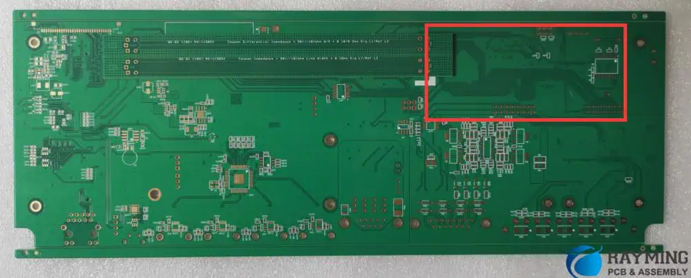
A board to board connector pcb to pcb connector is a connector that is used to join printed circuit boards (PCBs) together electrically and mechanically. These connectors provide reliable interconnections between boards, allowing signals and power to be transmitted. With the continuing miniaturization of electronics, board to board connectors play a crucial role in packing more functionality into smaller products.

Board to board connectors come in a wide variety of styles, pitches, mounting configurations and materials to accommodate varied application requirements. From low speed signals in consumer products to high speed differential pairs in telecom systems – board to board connectors enable complex multi-PCB architectures across industries.

This article provides a detailed overview of board to board connector technology, architectures, attributes and selection factors when choosing the appropriate connector.

What is a Board to Board Connector?

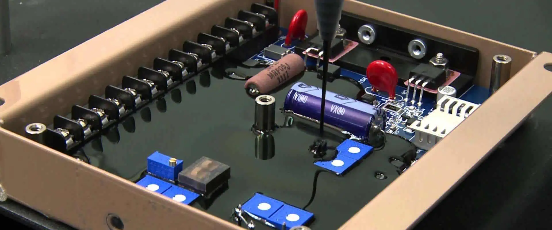
A board to board connector creates a removable electrical and mechanical connection between two or more printed circuit boards (PCBs). As opposed to cables and wires, these connectors allow boards to be stacked together achieving higher component density.

Some key characteristics of board to board connectors are:

  • Creates electrical connectivity for signals and power between PCBs
  • Provides mechanical rigidity securing PCB stack
  • Allows easy assembly/disassembly for repair or upgrades
  • Achieves higher density versus cables/wires
  • Facilitates high speed transmission with impedance control
  • Available in wide variety of pitches, interfaces and materials

Board to board connectors serve applications such as:

  • Stacking boards in electronic devices (cell phones, handheld devices)
  • Joining backplanes, midplanes and daughtercards (servers, network/telecom hardware)
  • Interconnecting boards in industrial, medical, defense systems
  • Testing/programming multi-PCB systems faster

With increasing functionality integration, board to board connectors enable optimized PCB-based system partition while retaining modular upgradability.

Types of Board to Board Connectors

Board to board connectors can be classified based on orientation, mounting style, contact type and interface. The four main architectures are:

  1. Board Stack Connectors: Vertical connectors that allow PCBs to be stacked one over another with signals routed across boards. Common type is header-receptacle.
  2. Mezzanine Connectors: Right-angle connectors that join motherboards to daughtercards/modules oriented parallel to each other. Common type is male/female header-socket strip.
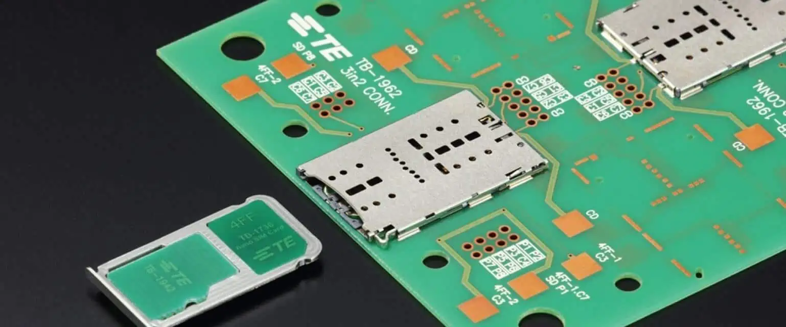
  3. Board to Board Edge Connectors: Connectors mounted on edge of PCB to route signals to backplanes, midplanes over short distances. Common type is plug-receptacle.
  4. Flex Cable Board to Board Connectors: Flex cables connecting two parallel boards using various interconnect technologies like ZIF, bottom entry, top entry.ArchitectureOrientationSpacingBoard StackVerticalSmall (<2.54 mm)MezzanineRight AngleMedium (>2.54 mm)Edge BoardParallelShortFlex CableParallelAdjustable

Table: Board to Board Connector Classification

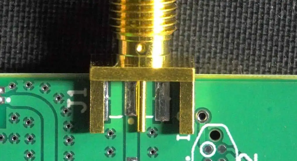
Additionally, board to board connectors may use interface/contact technologies like:

  • Pogo pins – spring loaded pins
  • Terminal pins – solid metal pins
  • Stamped contacts
  • Tuning fork contacts
  • MagJack – magnetic coupled contacts

This allows optimization of reliability, density, speed and power delivery across various applications.

Advantages of Using Board to Board Connectors

Board to board connectors offer several benefits versus traditional cabling:

Size: Enables dense vertical stacking of thin PCBs not feasible with cables

Speed: Allows matching impedance up to speeds > 25 Gbps with X, Phi contacts enabling high speed differential signals

Simplicity: Single interconnect solution from board to board without need of cable assembly and attachment points

Serviceability: Connectors allow quick insertion/removal of boards for maintenance, upgrades compared to cabled connections

Flexibility: Wide range of stackup, routing, layout, material and plating options available off the shelf from vendors

Cost: Volume economics combined with ease of assembly/servicing provides lower total cost at system level

With miniaturization, speed and edge computing trends – board to board connectors serve an important role in packing more functionality per unit volume across applications.

Key Characteristics of Board to Board Connectors

There are several key parameters to consider when selecting a board to board connector for an application from the myriad choices. These should be analyzed relative to mechanical, electrical and environmental requirements:

1. Pitch: Centerline distance between adjacent contacts/pads in connector. Pitch selection impacts stack density, routing constraints, noise coupling. Common pitches range from 0.4 mm to 5 mm.

2. Current Rating: Maximum current supported by connector pin and board traces. Important for power transmission to boards. Range is usually 0.5A to 15A.

3. Signal Pairs: Number of differential pairs the connector can support. Key for multi-gigabit interfaces using high speed serial links. Range is from 1 pair to 20+ pairs.

4. Stack Height: Distance between top and bottom PCBs, set by connector length. Affects overall system profile. Typical range is 5 mm to 60 mm.

5. Contact Type: Contact style tuned for signals (tuning fork), power (solid pin) or both. Affects reliability under thermal, vibration conditions.

6. Mounting Style: Mounting mechanism of connector to board. Common types are thru hole, surface mount, press fit, solderless. Impacts ease of assembly/servicing.

7: Alignment**: Precision guiding features to control co-planarity, alignment across stacked boards. Reduces misalignment issues.

8. Actuation: Mate/de-mate activation style from automatic, tool-less manual to assistive actuated types. Important for field replaceability

9. Environmental sealing: Gaskets, housing seals to prevent dust, moisture, EMI ingress for reliability. IP ratings specify degree of protection.

Above parameters for board to board connectors must be evaluated vis-a-vis mechanical requirements (vibration, shock, system profile), electrical needs (signal speeds, ampacity), assembly constraints (automation or manual steps) and environment factors (sealing, humidity, pollution degree).

Application priorities would drive selection across this range – from a 0.4 mm pitch mezzanine signal connector to a ruggedized 5 mm pitch duo-beam power connector. Interconnect modeling early in the design phase is crucial to make informed decisions balancing these tradeoffs.

Board to Board Connector Materials and Platings

Connector contacts go through millions of insertion cycles requiring materials tuned for strength, conductivity and environmental resilience. Key connector component materials include:

Contact Material

  • Copper Alloys: phosphor bronze, beryllium copper. Most common offering combination of strength and conductivity for signals. Lower cost.
  • Stainless Steel: Good strength properties and resistance to vibrations and corrosive atmospheres. Used for higher reliability connections.
  • Brass: Economical material for low frequency power transmission when contact resistance not critical.

Plating

  • Tin: Basic economical plating. Prone to oxidizing (tin whiskers) which increases contact resistance over lifetime
  • Gold: Does not oxidize. Excellent environmental resistance and minimizes contact resistance. Most common for high reliability despite higher cost.
  • Palladium or Palladium Nickel alloy: Intermediate choice offering oxidation resistance at lower cost profile versus gold.

Insulator Material

  • Plastics: Most common formula being high temperature engineered thermoplastics like PEEK, PPS, LCP due to combination of dielectric strength, toughness and temperature rating
  • Ceramics: Used when very high dielectric strength and temperature properties needed despite fragility considerations.

Choice of materials also extends to mechanical components like connector housing, board locks, shields etc in addition to contacts and insulators which are taking the electrical transmission load. This determines mechanical robustness, sealing effectiveness and system level reliability over product lifetime.

Board to Board Connector Interface Comparisons

pcb-connectors-wire-to-board

Some application considerations and tradeoff comparisons between popular board to board connector interfaces are shown below – from industrial/consumer applications to commercial/defense systems:

Application Key Needs Interface Choice Tradeoffs
Smartphones, Tablets Thin, light, low cost Board Stack 0.4mm pitch Lower power, dust ingress issues
Handheld Medical Devices Signal integrity, contact reliability Mezzanine 1mm FR4 Tuning fork Higher cost, medium density
ATE Board Testers High mating cycles, shock/vibe Press fit tuned for cycles Needs PCB keepouts, via transitions
HPC Server Risers Power delivery, thermal, field replaceable Current Sense Pogo Pin Tall profile, manual actuation
Routers, Switches Signal integrity at speed, heat dissipation Tuning fork phi contacts Precise alignment features key
Rugged Laptops Vibration, EMI sealing, power/signal combo Metal shielding, combo pins Design complexity, thermal loads
Avionics vetronics Hermetic sealing, corrosion resistance Glass seals connectors Less replaceable, special handling

Table: Board Connector Interfaces Compared Across Applications

As can be seen, there is significant variety in best fit board to board connectors depending on end system requirements, environmental needs and product lifecycle considerations. Getting these interconnects right is vital to long term reliable functioning of electronic systems and hence rigorous modeling and testing is emphasized by experts before commitment to production.

Trends in Board to Board Connectors

Some key trends shaping board to board connector evolution driven by customer applications are:

1. Higher Density Interconnects: To pack more functionality per unit volume, there is drive towards fine pitch (>0.5 mm pitch) connectors plus multi-row architectures. This sets reliability challenges due to coplanarity demands requiring advanced SMT equipment.

2. Power Delivery: To feed increasing compute cores, GPU and memory needs – power currents per pin rising with high amp 12V, 5V, 3V standards needing reliable delivery. Innovative power-signal optimized contacts and filtering being adopted.

3. Higher Signal Speeds: Multi-gigabit Serdes speeds going from 25 Gbps towards 50-100 Gbps per differential pair adopted in server, network applications. This requires impedance control, crosstalk minimization and EMI shielding for signal integrity.

4. Ruggedized Design: Vibration damping, sealed connectors designed for harsh shock, moisture, contamination and wide temperature variations seen in defense, industrial uses. This demands analysis beyond standard commercial specs.

5. Tool-less Assembly: Solder-less press fit connectors gaining adoption due to ease of automated or manual board stacking avoiding solder process reliability issues and hazards. Self-alignment and mating hardware aids this goal.

Above trends demand modeling interconnects in detail prior to launch and working closely with connector vendors to get appropriate solutions matched to application needs from product inception.

Best Practices for Board to Board Connector Selection

Selecting the optimal board to board connector solution entails following key steps:

1. Setting Requirements: Define interface density, maximum data speeds, power needs, mechanical stackup, environmental factors based on product’s use cases and customer expectations. These serve as guiding functional requirements.

2. Modeling Constraints: Identify interface routing topologies, spacing rules, component placements constraints based on PCB and enclosure design architectures.

3. Research connector technologies: Explore industry standard interfaces plus latest proprietary innovations from connector vendors to generate viable shortlist matching needs.

4. Simulate Performance: Component level modeling using SPICE models and 3D EMI/Thermal simulations establishes electrical, environmental integrity checking mechanical robustness with shock/vibe and thermal desktop testing.

5. Prototype evaluation: Validate connector design performance with solder down prototypes pcba put through environmental stress screening and electrical tests measuring signal integrity under dynamic conditions faced over product lifecycle.

6. Volume Manufacturing Planning: Lock down board to board connector supplier providing modeling support up front to aide successful volume manufacturing, meeting regulatory compliance plus supplying to service spares for maintenance repairs over total lifespan.

Above best practice methodology avoids pitfalls of over-specifying connector just based in paper specs versus modeling it within system use conditions plus locking reliability over total product life. This ensures the highest quality of connector selection decision.

Frequently Asked Questions

Q1. How are board to board connectors different from cable connectors?

Board connectors create direct mating between PCBs without need for cables or wires to route signals. This saves space, minimizes transmission loss. But connectors have lower current ratings than cables, limit flexible routing.

Q2. How many insertion cycles do board to board connectors support?

Most connectors are specified for 100-500 mate/de-mate cycles for low end industrial/consumer applications while high end mezzanine connectors used in server/network applications support 500 to 1500+ cycles.

Q3. Do board connectors work for flexible or rigid-flex PCBs?

Yes, flexible connectors using flex cable wiring or ruggedized board stack connectors work for directly stacking flex PCBs. Care must be taken to minimize flexing damage with strain relief.

Q4. What are common mounting styles for board connectors?

Thru-hole pin is most common but surface mount, press fit tuning fork contacts are gaining adoption for automated assembly. Hybrid mounting allowing both permanent and field replaceable connections also exist.

Q5. What modeling tools are used for board connector design validation?

Platforms like Ansys HFSS, Ansys Q3D for EMI/signal integrity analysis. Ansys Mechanical, Solidworks Simulation for thermal plus structural modeling leveraged along with SPICE models.

Summary

Board to board connectors serve a vital interconnection role in electronic systems allowing signal and power transmission across stacked PCB architectures in space constrained compact product packaging.

With increasing focus on high speed multi-gigabit interfaces, power delivery demands plus ruggedized designs – choice of the optimal connector solution through detailed modeling and validation ensures reliable system performance.

By following structured engineering processes to characterize mechanical, electrical and environmental constraints early while evaluating technology options – optimum board connector selection happens balancing density, speed, reliability and cost metrics delivering successful volume production.

Circuit Printing Easy Way: Machine, Process and Cost

Circuit printing refers to additive manufacturing processes that can directly print the electrical traces and components onto substrate boards to construct functioning electronic circuits. This revolutionary technology promises to greatly simplify laying out custom printed circuit board (PCB) designs without relying on complex fabrication steps.

As hobbyists and startups push innovation boundaries with highly complex boards, circuit printing now offers an easier alternative to traditional PCB making methods. This article provides a comprehensive overview of various aspects of circuit printing including – suitable equipment, underlying printing process, key materials as well as overall costs.

Benefits of Circuit Printing

Here are some of the major advantages of adopting circuit printing:

  • Allows printing functional electronics without harsh chemicals
  • Eliminates complex PCB fabrication steps like masking and etching
  • Accommodates rapid design changes through easy file modification
  • Enables embedding components within board itself
  • Achieves finer trace resolution than commercial PCBs
  • Allows printing unconventional substrate materials
  • Simpler and cheaper than CNC milling or laser cutting
  • Faster concept validation by instantly printing inventions

For rapid prototyping needs, circuit printers greatly simplify constructing new ideas.

Types of Circuit Printers

Custom PCB Printing
Custom PCB Printing

Various types of printing technologies allow additive formation of electrical circuit boards. The main circuit printing methods include:

Inkjet Printing

Uses piezoelectric print heads to jet tiny droplets of special conductive inks to draw circuit layouts on thin substrates.

Aerosol Jet Printing

Employs an aerodynamic focusing nozzle to atomize conductive ink into a dense aerosol spray which gets printed.

Nano-particle Jetting

Proprietary process utilizing gas flow to deposit metal nano-particle inks through an array of jet heads to print tracks.

Direct Ink Writing

Uses robotic 3D micro-extrusion of viscoelastic silver & graphene pastes to print free-standing wires without support.

Laser-Induced Forward Transfer

Lasers pulse to propel tiny volumes of conductive ink onto boards thus printing complex patterns with no masks.

Desktop sized circuit printers costing under $5000 target hobbyists and startups exploring innovative electronics ideas.

Circuit Printer Machine Considerations

When selecting circuit printers, key factors to evaluate include:

Print Resolution โ€“ Finer nozzle diameters allow more intricate circuits but reduce throughput. 100 ฮผm lines are standard.

Print Speed โ€“ Print heads with higher jetting frequencies speed up printing larger boards. Minimal movement also boosts rates.

Supported Inks โ€“ Printers are usually optimized for certain proprietary conductive/resistive/dielectric ink chemistries.

Substrate Handling โ€“ Flatbed printers accommodate rigid boards up to 300mm x 500mm size while roll-to-roll printers suit flexible films.

Layer Registration โ€“ Precision board alignment for printing multi-layer circuits without shorting between layers.

Software Workflow โ€“ Seamless data interface from PCB design to printer interface to executing print runs quickly.

Cost โ€“ Desktop printers provide an affordable entry point but offer lower resolution and accuracy versus industrial solutions.

Analyzing application needs and production expectations guides appropriate printer selection.

Circuit Printing Process Overview

The typical circuit printing workflow involves:

1. Design – Creating required circuit layout in CAD software

2. File Conversion – Generating printer-specific file formats like Gerber/SVG/HPGL etc.

3. Substrate Loading – Mounting suitable board blank onto printer bed

4. Alignment – Precisely positioning substrate by optically detecting fiducials

5. Printing – Executing conductive ink deposition toolpaths

6. Drying – Using heaters or UV lights to quickly cure printed ink

7. Testing – Validating printed trace continuity and absence of shorts

8. Component Assembly – Mounting and soldering surface mount devices to complete circuit

This additive printing process revolutionizes laying out custom circuit boards.

Circuit Printing Materials

PCB Screen printing

Specialized conductive and dielectric inks made using nano-particle metals and insulating polymers form the foundation for circuit printing.

Conductive Inks

Silver, copper or graphene based particle inks dispensed from cartridges serve to print the electrically functional traces and pads. Only 10-15% metal loading by weight is required for conductivity.

Dielectric Inks

Insulating acrylic-epoxy formulations precisely printed to encapsulate crossed-over traces or define soldermask areas prevent shorting while providing structural base.

Substrate

Materials like FR4, flexibilized PET/PC films, paper or textiles act as the foundational board blank to print circuits atop.

By developing custom inks tuned for stability and printability, a wide spectrum ofsubstrate materials can be transformed into functional electronics.

Design Rules for Printable Circuits

To effectively fabricate a circuit layout by printing, the PCB artwork must comply with certain constraints related to printhead capabilities, ink performance etc.

Follow these guidelines when designing circuits targeting additive printing:

1. Define minimum wire width: Static droplets constrain resolution so widths >= 100 microns print well.

2. Set spacing rules: Gap between adjacent traces should exceed nozzle diameter to prevent bridging shorts.

3. Minimize acute angles: Gradual bends aid continuous ink flow compared to tight angles risking interruptions.

4. Allow conductor overlaps: Intersecting traces should overprint each other slightly for reliable connections after curing.

5. Include fiducials: Printer camera detects board reference points like cross marks to align subsequent layers precisely.

6. Ink volume limits: Constrain total length x width of traces printed to avoid printhead clogging and downtime.

7. Validate DFM: Printer manufacturer design rule checks validate artwork suitability before actual printing.

Accounting for process-specific capabilities allows achieving high circuit print yields.

Layer Registration Accuracy

For reliable multi-layer circuit printing, accurate alignment between printed layers is vital to prevent electrical shorts. High precision is achieved through:

Precise Stages โ€“ Printer beds featuring linear drives, precision ground rails, and/or air bearings offer highly repeatable X-Y positioning.

Vision Systems โ€“ Onboard cameras and optical recognition algorithms provide accurate positional feedback for registration.

Fiducial Marks โ€“ Cross hair squares or circle center alignment patterns on each board layer serve as layer-to-layer image detection points.

Software Compensation โ€“ Any residual distortions are digitally compensated through warping printed image to match earlier layers.

Advanced printers provide 5-10 ฮผm registration accuracy allowing dense multilayer circuits with traces pitched at 200-400 ฮผm.

Sintering Process

Once printed, the deposited conductive ink traces require controlled heating to evaporate carriers, melt nano-particle metals and form connected solid tracks in a process called sintering.

Sintering drives off solvents and enhances inter-atomic diffusion bonding between particles to increase electrical conductivity. This fixation transforms printed patterns into functional traces.

Rapid photonic curing systems using high intensity pulsed light provide instantaneous selective sintering without degrading delicate substrates. Sintering occurs in seconds depending on volume to solidify prints.

Printing Cost Analysis

Evaluating the cost implications of adopting circuit printing involves:

Printer Equipment โ€“ Desktop printers for under $5000 target hobbyists while advanced inkjet printers suited for small-scale production can cost over $75,000.

Printed Electronics โ€“ Conductive inks price around $300 per liter while dielectric inks cost ~$200 for insulation and encapsulation.

Substrates โ€“ Base materials like FR4 blanks are $10-30 per square feet area depending on thickness. Flex PCB grades cost extra.

Ancillary Tools โ€“ Additional sintering systems, curing equipment, testing stations etc. entails further expenses.

Operator Labor โ€“ Prep time for file processing, setup, postprint steps require manual intervention so factor hourly rates.

For low volume printed electronics, equipment depreciation influences cost prominence while material and labor dominate for mass production economics.

Advantages over Conventional PCBs

Printed circuits offer many benefits compared to traditional rigid FR4 boards:

Simpler Fabrication โ€“ No repetitive masking, etching, stripping steps involved allowing faster prototyping.

Design Flexibility โ€“ Changing layouts only requires updated print file instead of regenerating entire fabrication process.

Substrate Versatility โ€“ Choice of foundation materials like textiles, polymers beyond just rigid laminates.

Environmental Sustainability โ€“ Process avoids using toxic chemicals required for conventional PCB manufacture.

Embedding Capability โ€“ Can directly print passive components like resistors/capacitors integrated into the board.

Superior High-Frequency Performance โ€“ Direct write circuits have smooth coplanar traces allowing high frequency operation.

Applications of Printed Electronics

The capabilities of printed electronics are enabling promising applications such as:

Wearable Devices โ€“ Directly printing circuits onto fabrics allows creating smart garments flexibly conforming to ergonomics.

Medical Sensors โ€“ Soft biosensors can monitor patient health parameters seamlessly when mounted directly on skin by printing.

Smart Packaging โ€“ In-mold electronics printing before injection molding plastic enclosures simplifies integrating circuits into products.

RFID Tags โ€“ Additively printing antenna and chip bonding lands greatly simplifies fabrication of wireless tags.

PE Textiles โ€“ Inkjet printing conductive patterns onto apparel can create flexible thin heating pads or illuminated clothing.

Automotive Displays โ€“ Low temperature deposition is ideal for directly printing polymer electronics onto curved surfaces inside cars.

Printing advancements offer electronics beyond mechanical PCB substrates to applications requiring form factor flexibility where conventional boards remain incompatible.

Limitations of Printed Electronics

While constantly improving, circuit printing technology still poses certain limitations presently:

Line Resolution โ€“ Printed traces remain thicker than photolithographic processes so circuits cannot miniaturize further.

Registration Accuracy โ€“ Overlay printing multiple ink layers precisely to prevent shorting between crossing conductors faces challenges.

Ink Stability โ€“ Ensuring shelf-life before particle settling as well as preventing printhead nozzle clogging need improvements.

Print Speeds โ€“ Additively generating intricate multilayer boards takes longer production time versus batch processing PCBs.

Conductor Quality โ€“ Achievable conductive ink resistivity still lags behind bulk copper tracks restricting high power applications.

Substrate Variety โ€“ Material compatibility still limits directly printing onto several advanced composites.

Further development of printing systems, inks and substrates continues to push boundaries lowering barriers to adoption.

Conclusion

Circuit printing promises to transform laying out even complicated electronics inventions by replacing tedious fabrication steps through direct material deposition. What used to rely on skilled technicians and days long process now gets simplified to instantly printing from CAD models inhouse. By merging printed electronics together with conventional components onto builder friendly substrates, innovators can bring product concepts to life faster and cheaper than ever before. Despite certain lingering limitations around ultimate miniaturization potential, registration needs and conductor quality, the ease-of-use and customization possible with printed circuits constitutes an invaluable asset during early development phases for enterprises and individual inventors alike. With global initiatives around environmentally progressive manufacturing also gaining prominence, it seems certain that printed electronics will continue making inroads providing simpler circuit foundations across an ever expanding slate of imaginative applications.

Frequently Asked Questions

Here are some common queries regarding circuit printing:

Q: What materials are used for printing substrates?

A: Paper, PET, PC and textiles allow low temperature deposition. Ceramic coated metal foils offer higher temperature stability. Composite boards also enable directly embedding printed electronics.

Q: What is achievable PCB line width resolution?

A: Most printers can achieve around 100 ฮผm line width and 125 ฮผm line spacing reliably. Ultra-precision systems approach 25 ฮผm resolution but remain slower.

Q: Are printed circuits as conductive as copper boards?

A: Ink curing generates around 2-5x bulk resistivity relative to rolled copper so high power density boards still favor etched metal tracks today.

Q: Can components be directly printed onto boards?

A: Modern ink chemistries allow co-printing simple resistors, capacitors, antennas alongside conductors in a single pass but traditional SMD devices still need manual attach.

Q: How accurate is layer-to-layer registration?

A: Advanced Industrial printers ensure registration accuracy within 5-10 ฮผm allowing reliable interlayer interconnections at 200+ ฮผm pitch. Hobby printers remain ~50 ฮผm.

How to CNC Your PCB Prototype Board

Computer numerical control (CNC) machining is an essential part of taking your printed circuit board (PCB) design from prototype to production. CNC milling accurately fabricates complex 2.5D and 3D features on custom PCBs that cannot be achieved with traditional manufacturing means.

CNC machining removes unwanted copper from specified areas of the PCB through an automated, programmable process to shape the circuits as per the design files. This article provides a comprehensive overview of using CNC technology to machine your own PCB prototypes.

Benefits of CNC Machining PCBs

Here are some of the major advantages of using CNC milling for PCB prototyping:

  • Creates functional prototypes from CAD models faster
  • Enables fabrication of multi-layer PCBs
  • Allows embedding active/passive components
  • Saves time and cost compared to outsourced small-batch PCB production
  • Achieves fine line width/spacing down to 125 ฮผm
  • Creates precision 2.5D contour milling not possible through etching
  • Allows micro-vias and buried vias for dense interconnection
  • Suitable for circuits with high-frequency, controlled impedance

By adopting CNC machining, PCB inventors can quickly implement and test ideas without relying on external factories.

CNC Machining Process Overview

The typical workflow for CNC milling PCBs involves:

1. Design – Creating the PCB layout in CAD software and generating CAM/Gerber files

2. Fixturing – Preparing the PCB blank and securing it onto the CNC machine bed

3. Probing – Work-piece coordinate system alignment to position the endmill over the board

4. Milling – Machining conductive traces by rastering the endmill per the toolpath

5. Deburring – Removing rough edges and burrs from milled conductors

6. Cleaning – Washing away milling debris and dust from the board

7. Visual Inspection – Checking for any shorts, opens or gouges

This basic process transforms the raw PCB blank into a finished board ready for component assembly and testing.

CNC Machines for PCB Prototyping

Various types of CNC machines like desktop routers, small-format mills, and mini-CNC machines are now available for machining custom printed circuit boards.

When selecting a CNC machine, key factors to consider are:

  • Workspace envelope (max PCB size)
  • Spindle speed and power
  • Supported endmills (diameter, length)
  • Drill precision and chip load
  • Software integration and workflow
  • Cost
Machine Description
Desktop CNC Routers Compact and affordable machines for home workshops good for double-sided PCBs up to 200mm x 300mm size
Small Format Mills Industrial grade machines with high spindle speeds and precision suited for faster, more intricate PCB milling
Micro-CNC Machines Specialized systems for milling tiny circuits like sensors down to 25mm x 25mm size with small endmills
Laser CNC Machines Uses a laser cutter instead of a router to ablate unwanted copper without physical contact

Desktop CNC routers provide an economical starting point for prototyping digital circuits at home or in makerspaces.

PCB Design Rules for CNC Milling

To effectively machine your custom PCB board, the layout must be designed while keeping CNC constraints and capabilities in mind.

Follow these key PCB design rules when targeting CNC fabrication:

1. Allow adequate tool clearances: Provide at least twice the cutter diameter as spacing around pads and traces for tool access. Account for tool shoulders too.

2. Include fiducials: Add alignment markers to use optical probing for coordinate system referencing before milling.

3. Set appropriate track sizes: Minimum trace width and gap should exceed bit diameter. A 10 mil end mill yields 8 mil lines.

4. Limit trace angles: Avoid acute angles zones as endmills cannot machine those properly. Use 45ยฐ/90ยฐ traces.

5. Define board outline: Clearly indicate board contours to machine the outline profile cut. Panelize designs for better fixturing.

6. Minimize vias: Countersunk holes need extra machining time so use judiciously. Bury only critical signals needing layer transitions.

7. Split ground planes: Machine inability to clear large copper areas will require intelligent splits.

By designing upfront for manufacturability, efficient, optimized CNC programs can be generated to machine the boards.

PCB Materials for CNC Milling

The blank PCB substrate selected influences suitable milling parameters and quality of machined traces. Important considerations when choosing CNC milling PCB materials include:

Machinability: Softer, non-glass reinforced substrates like FR-4 machine faster with lower tool wear. Rogers RO4000 series bonds well but have higher abrasivity.

Dimensional Stability: Lower expansion coefficient substrates sustain precision geometries despite heating during milling better.

Bonding: Good copper foil adhesion prevents lifting or tearing during end mill passes while poor bonding raises chances of delamination.

Heat Tolerance: Glass transition temperatures above the heat generated during milling ensures material retain its strength. Ceramic-filled substrates withstand higher cutting temperatures.

Standard 1.6mm FR-4 blanks with 1oz copper foil offer a reasonable starting point for DIY CNC milling PCB prototypes.

PCB CNC Milling Tools

PCB Milling

Carbide endmills are commonly used to remove unwanted copper when CNC machining PCBs. Various types of tools for specific applications include:

Rigid Endmills โ€“ Single piece solid carbide spiral flute tools for general purpose 2D contour milling of traces.

Ball End Mills โ€“ Carbide cutters with a ball tip to perform 3D contour machining for sculpted circuits.

V-Bits โ€“ ‘V’ shaped carbide mills used make trenches for rectangular milled traces.

Drills โ€“ High speed carbide micro-drills create holes for conductive thru-hole vias.

Diamond Cutters โ€“ Polycrystalline diamond tools prolong tool life when milling abrasive substrates like ceramic PCBs.

Proper feeds, speeds, stepovers and axial/radial depths based on tool geometries must be set for robust milling performance.

Fixturing Considerations for PCB CNC Milling

Even small PCB blanks can resonate and vibrate extensively during aggressive material removal if not properly secured.

Here are some guidelines for reliably fixturing PCBs to withstand milling forces without movement:

  • Use a spoilboard/sacrificial layer between PCB and machine bed
  • Low profile clamps distribute holding forces closest to milling zone
  • Vacuum beds utilize negative pressure for forceful workholding
  • Adhesives temporarily bond board directly to spoilboard
  • Add stiffening ribs or perimeter supporting fixtures structures
  • Employ self-indicating pressure sensitive films to map grip distribution

Since PCBs expand on heating up during milling, use slip sheets or boundary constraints to permit thermal expansion.

PCB CAM Processing

To translate the PCB layout into toolpaths executable on a CNC machine, CAM (computer-aided manufacturing) software is necessary.

CAM software allows:

  • Importing Gerber, ODB++ and other standard PCB file formats
  • Specifying machine, tools and stock model
  • Setting pass depths, stepover parameters
  • Defining toolpaths (traces, outlines, holes etc.)
  • Simulating milling process visually
  • Calculating accurate cycle time estimates
  • Generating machine-ready G-code programs
  • Adding fiducials markers for probing

With optimal CAM strategies and post-processing, the milled quality of even high density PCBs with 6 mil lines/spaces can approach conventional PCB etched limits.

PCB Probing and Datuming

pcb-cnc-router

To accurately align the CNC endmill over desired regions of the blank PCB, probing is necessary. This establishes a coordinate system to locate all toolpath positions correctly relative the board.

Workflow:

  1. PCB loaded and clamped to machine bed
  2. Camera centers board in view field
  3. Touch probe electrically contacts added fiducial points
  4. Software records exact coordinate values
  5. Completed board profile aligned to programmed paths

Fiducials as reference datums may be:

  • Round pads โŒ€ 0.5 to 1 mm
  • Square pads 1 mm
  • Drilled holes 1 mm diameter
  • Slot or edge markers

Datuming compensates for variations in blank positioning and allows achieving reliable, repeatable milling quality.

PCB CNC Milling Feeds and Speeds

The cutting parameters specify the velocity (feed rate) at which the endmill machines the PCB traces as well as its spindle RPM. This impacts:

  • Material removal rate
  • Cutting forces and torque
  • Tool wear
  • Machined edge finish
  • Process cycle time

General guidelines for initial PCB milling parameters:

Spindle RPM โ€“ 15,000 to 20,000 RPM

Feed Rates โ€“ 50 to 150 mm/min

Higher number of flutes, adept use of climb versus conventional milling and optimizing chiploads boosts performance. Rigid fixturing is vital for chatter-free milling.

PCB CNC Milling Strategies

Various toolpath strategies exist to clear copper regions when isolating PCB conductors. Key methods include:

Trace Isolation Milling

Thin parallel passes with a certain overlap percentage traces out individual conductors by removing material between them. 50% overlap is commonly used balance cycle time and surface finish. Wider traces may allow faster 75% stepover overlap passes.

Slotting

plunge cutting trenches on both sides to define rectangular milled traces. Requires two pass milling but prevents copper burrs compared to outline milling.

Area Clearance Strategies

Fitting path rasters, direction parallel passes or adaptive clearing patterns remove large copper zones efficiently while preventing tool overload.

Drilling for Vias

Peck drilling, chip breaking and regular retracts during hole boring helps chip evacuation and prevent clogging to achieve clean vertical via holes.

Proper path sorting, entry/exit strategies and optimal tool orientation further boosts milling performance.

Post Processing Steps after PCB CNC Milling

After machining the board, some secondary processing steps help improve milled PCB quality:

Deburring โ€“ Removing rough copper edges around traces manually or through automated abrasive flow deburring equipment.

PCB Washing โ€“ Thorough cleaning with pressurized water jet sprays or PCB immersion tanks removes swarf, debris and dust.

Nickel Plating โ€“ Electroless nickel coating prevents copper traces from oxidation and improves solderability.

Electrical Testing โ€“ Validating continuity between intended conductors and absence of any shorts with a multimeter probe.

Visual Inspection โ€“ Microscope checks at 30X to 60X magnification confirm channel integrity with no copper smearing or gouges.

These post processing steps enhance machined PCB quality to build fully functional boards.

Lean Manufacturing Aspects

Adopting lean manufacturing principles maximizes CNC machine utilization, optimizes changeover times and improves productivity when milling PCB prototype boards in low volumes.

Some lean aspects that can boost efficiency are:

  • Standardized fixturing elements for quick loading
  • Color-coded setup components
  • Shadow boards to organize endmills by type
  • Custom macros for common parameter sets
  • Probe routines to expedite referencing
  • Storage racks near machines for ready access
  • Digital status indicators for free capacity
  • Preventive maintenance during machine downtime
  • Setup templates to minimize changeover time

With enhanced workflow management, CNC milling works well for fast fabrication of digitally designed PCB innovations.

Advantages over PCB Etching

Strip film etching line

While chemical etching can produce basic PCBs, CNC machining offers many advantages:

Precision โ€“ Endmills can create fine details with tighter tolerances and superior dimensional accuracy than etching.

Reliability โ€“ Milling gives positively isolated traces instead of undercuts prone tracks from over-etching.

Consistency โ€“ Automated machining ensures uniform channel widths across the board unlike etching.

Flexibility โ€“ No need to generate etching masks. Easy to rapidly rework designs by just updating toolpaths.

Functionality โ€“ Can fabricate high density boards impossible through etching like 8-12 layer multilayer boards with blind/buried vias.

As DIY hobbyists push circuit complexity, CNC fabrication provides better reliability and performance.

Limitations of PCB CNC Milling

Some inherent limitations still constrain achievable quality levels relative to commercial PCB production using lithography when CNC milling prototypes:

  • Surface finish not as smooth as commercial PCBs
  • Maximum millable trace density lower than masking/imaging limits
  • Restricted to proto-run volumes given process throughput
  • Face milling constrains layer alignment precision unlike precision lamination
  • Higher initial setup costs for CNC systems compared to etching
  • Still requires manual assembly of components unlike SMT lines
  • More process expertise needed to generate toolpaths, set parameters etc.

But the ability to quickly iterate innovative board designs provides tremendous value despite these technology restrictions.

Safety Precautions

CNC milling PCBs poses some unique hazards requiring appropriate precautions:

  • Rotating tools can violently throw loose debris when they snag so secure workpieces and nearby objects
  • Always keep hands away from moving machine elements with awareness barriers around work zones
  • Wear safety glasses to prevent eye injuries from chips and guard against particulate inhalation
  • Fire risk exists as insightsulative swarf ignites so have extinguishers and avoid combustion sources nearby
  • High pitch noises mandate using hearing protection plugs or noise cancelling headgear
  • Allow hot milled PCBs to adequately cool down before handling to prevent finger burns

With training and adoption of safe working habits, CNC milling provides a very versatile PCB prototyping choice.

Conclusion

As PCB designs increase in complexity with shrinking geometries and rising interconnect densities, CNC milling delivers fabrication capabilities scaling beyond chemical etching limits for prototyping digital logic circuits and high frequency analog boards alike. With easy desktop solutions now available, electrical engineers can cost-effectively implement innovations using agile inhouse milling. By applying appropriate design principles and CAM strategies, even 0.006 inch trace channels are realizable. While certain accuracy and volume barriers remain relative to mature PCB production ecosystem, the quick turnaround enables by CNC milling delivers huge savings in development costs through rapid design revisions. With sufficient fixturing, process expertise and safety precautions, CNC technology constitutes the future of PCB prototyping for innovators.

Frequently Asked Questions

Here are some common queries regarding CNC PCB milling:

Q: What PCB materials can be machined well?

A: Standard FR-4 material with 1oz foil bonds nicely without cracking for small prototype runs. Rogers RO4000 series works too but requires reduced feeds. Ceramic PCBs require diamond coated endmills.

Q: What should be the minimum clearance between traces?

A: Its ideal to keep >= 2 times tool diameter as spacing through isolation paths are generated around traces so a 10 mil cutter needs >= 20 mil gaps.

Q: Can CNC mill complex boards like 12 layer multilayers?

A: Yes, with a precision production CNC machine allowing variable Z-depth machining, complex multilayer PCBs can be section milled layer-by-layer by adjusting milling depth per pass.

Q: What tolerances are achievable while milling PCBs?

A: With tight fixture schemes and dialing in appropriate parameters, machining accuracy of +/- 0.003″ is definitely feasible meeting typical PCB needs. Precision systems can further boost accuracy.

Q: How to prevent short circuits between traces after CNC milling?

A: Perform visual inspection at high magnification after milling to check for insulation smearing. Alternatively, apply immersion tin plating to fully coat exposed copper traces preventing inter-channel shorts.

Why Is Controlled Impedance So Important in PCB Design ?

impedance control pcb

Controlled impedance constitutes one of the most crucial considerations in modern high-speed printed circuit board (PCB) design. Simply, impedance represents the opposition to electrical current flow within the board. Controlled impedance tracks ensure the PCB environment presents consistent impedance to critical signals.

Maintaining proper impedance matching along transmission paths allows clean signaling critical for high frequency applications. Uncontrolled impedance introduces reflections and losses degrading signal integrity. This article details what impedance entails, why control ranks so necessary in circuits along with methods to master impedance in layouts.

YouTube video

What is Impedance?

In PCB design, impedance refers to the apparent resistance presented to electric current flow along a conductive trace. It encompasses the comprehensive opposition considering capacitive, inductive and resistive properties of the materials comprising the circuit path.

Impedance changes with operating frequency as reactive elements take effect. It defines the voltage / current ratio at a given frequency:

Impedance (Z) = Voltage / Current

The impedance depends on inductance (L), capacitance (C), resistance (R) inherent to the trace and surrounding environment:

Z = โˆš(R + jฯ‰L)2 + (jฯ‰C)2

R โ€“ Sheet resistance of copper trace
L โ€“ Self-inductance along trace
C โ€“ Capacitance to reference planes

At low frequencies, resistive terms dominate. At higher frequencies, inductive and capacitive elements impose impedance. Controlling factors like dielectric constants and trace dimensions dictate the impedance response a signal encounters in a PCB channel.

Why Control Impedance?

PCB Impedance

Uncontrolled impedance causes signal reflection issues leading to overshoot, ringing artifacts and data loss that impedes reliable operation at Increased operating frequencies. Control supports signal integrity.

1. Prevent Signal Reflections

High-speed signals require matched source, transmission line and load impedances to absorb the full signal. Mismatched impedance causes partial wave reflections interfering with the original signal.

Even minor impedance deviations lead to disproportionate reflectance with more noise disrupting faster, higher frequency signals. Reflections degrade rise times and jitter degrading bit error rates. Controlled tracks prevent reflections.

2. Facilitate Impedance Matching

Source and load components assume designed impedance values for interconnects – typically 50 ฮฉ or 100 ฮฉ differential. Traces must match anticipated impedance ensuring necessary termination resistors properly damp signals.

Mismatched lines over/under load termination networks hampering absorption of fast transient edges. Controlled lines present expected impedance for matching components.

3. Reduce EMI Radiation

Uncontrolled impedance increases high frequency return loss and ringing which worsens electromagnetic interference (EMI). Controlled lines help confine signals avoiding unintended radiation that risks coupling into nearby susceptible circuits.

In summary, controlled impedance traces counteract reflections, absorb signals cleanly, and reduce interference – critical factors for reliable high-speed PCB functionality.

How to Achieve Controlled Impedance?

Core-built PCBs impedance control

Adjusting physical PCB parameters allows tuning impedance to target values along traces mitigating unchecked variations:

1. Trace Width

The main conductor width sets baseline impedance value. Wider lines decrease; narrower traces increase impedance assuming uniform thickness.

2. Dielectric Stackup

Dielectric material type and thickness surrounding traces heavily influences impedance based on inherent capacitance. Tighter dielectrics raise values.

3. Reference Planes

Closeby continuous reference planes augment capacitance lowering impedance. Spread planes raise impedance by reducing coupling.

4. Trace Separation

Spacing between signal and surrounding traces, pads or void areas impacts coupling determining impedance.

By tuning parameters appropriately, target impedance achieves matching. Advanced fabricators carefully model stackup dimensions and material electrical properties to yield controlled impedance across routing layers.

Controlled Impedance Target Values

Differential Impedance

While impedance ranges widely, two target values dominate modern PCB layouts:

50 ฮฉ Impedance

  • Standard controlled impedance used for single-ended signals
  • Matches source/load termination resistance
  • Requires narrower traces with tighter reference planes

100 ฮฉ Differential Impedance

  • Typical value for differential pair routing
  • Wider trace spacing balances capacitive coupling
  • Closer planes increase capacitance

Many factors determine choice of target impedance for a design but these two levels handle majority of applications. Control resolution within +/- 10% desired.

Traces get clearly marked in layouts meeting controlled spec after extensive modeling. Strict dimensional tolerances maintained throughout fabrication for consistency.

How Accurately to Control Impedance?

Edge-Coupled Stripline (symmetrical) pcb impedance control

Extremely tightly controlled impedance better maximizes signal quality but demands much higher process capabilities driving up cost. Reasonable tolerances work for most applications.

A useful way to consider controlled impedance accuracy:

Impedance ControlApplication
+/- 5-10 ฮฉHighest speed RF boards >5 Gbps
+/- 10%Fast digital 2-5 Gbps
+/- 15%Slower bandwidth below 2 Gbps

Realistically, impedance depends on many interrelated factors that individually influence values as much as +/- 20% even on controlled lines:

  • Copper thickness
  • Dielectric composition
  • Trace locate position
  • Layer registration
  • Fabrication accuracy

Well characterized PCB processes keep deviations reasonably constrained. But extensive modeling best informs expectations when pushing higher frequencies.

Controlling Impedance in PCB Layout

Beyond smart stackup, layout practices greatly aid achieving impedance control and timing across routing:

  • Minimize length variance between differential pairs
  • Match lengths through vias and layers
  • Eliminate acute angle turns on traces
  • Avoid impedance discontinuities
  • Validate with impedance analysis

Careful layout adhering to controlled parameters ensures PCB environments present consistent, matched impedance to facilitate high-speed signaling.

When are Controlled Impedance Lines Necessary?

Edge-Coupled Surface Microstrip pcb impedance control

Controlled impedance traces help maximize signal quality and reliability but come with fabrication difficulty and cost impacts. Reserved only for necessary nets, some key considerations around usage include:

Clock Signals

High frequency clocks over 100 MHz propagate fast rise times requiring impedance control to prevent skew between board sections. Route clock trees through controlled dielectric layers.

SerDes Data Lines

High speed serializer/deserializer data channels demand matched impedance environments to limit reflections between source and destination components.

Analog Lines

Mixing uncontrolled digital routing can introduce noise into analog signals. Maintain impedance through analog channel length including shield layers for isolation.

Memory Buses

Address/command/data buses to RAM devices with clock/strobe signals benefit from consistent impedance routing to time signals reaching memory IC pads.

In summary, controlled impedance applies to nets with high frequency components or susceptibility. Matching impedance ensures quality signaling over traces, through vias across layers in the PCB stackup.

Implementing Impedance Control

pcb impedance test coupon

Achieving impedance requires coordination across design stages:

Simulation

Model anticipated stackup with projected dielectric constants and trace dimensions to calculate expected impedance. Assess termination schemes and line lengths.

Stackup Planning

Specify laminate materials, prepreg, copper weights, and layer sequencing to achieve impedance targets while meeting isolation needs.

Layout

Carefully route wide/narrow traces in controlled dielectrics with referenced return planes maintaining consistent geometry.

Fabrication

Precisely process board layers under strict dimensional tolerances keeping registered alignment. Test coupons validate continuity.

Verification

Employ impedance analysis to identify undesired variations exceeding limits needing layout adjustments or review of process assumptions.

While controlled impedance layout ability steadily improves in PCB tools, fabricators also enhance dimensional accuracy and stackup repeatability easing the challenge of impedance control for designers.

Overview of Controlled Impedance Advantages

In summary, controlled impedance tracks bring major high-frequency signaling benefits:

  • Prevent reflections that distort signal rise times
  • Enable impedance matching to properly terminate lines
  • Reduce EMI from uncontrolled ringing
  • Maintain fast switching speeds and data integrity
  • Ensure high bandwidth with low bit error rates
  • Critical for multi-gigabit SERDES channels

As data rates continue increasing, controlled impedance applies to an expanding range of chip-to-chip nets. Constraint driven trace width, spacing and layer planning facilitate quality high-speed signaling.

FAQ

Why is impedance matching important?

Impedance matching means source, transmission line and load all share common impedance preventing signal reflection allowing full absorption of wavefronts. Clean signaling relies on matched impedance environments.

What is Copper Pour in PCB?

A copper pour (or area fill) in printed circuit board (PCB) design refers to a large solid conductive area that floods sections of the board with copper. This acts as a versatile supplement to conductive traces to provide enhanced functionality.

Pours seamlessly fill open regions of the PCB layers with copper creating polygons connected to a net. They integrate as part of the circuit connecting components while facilitating power distribution, shielding, cooling and rigidity.

Well implemented pours bring several benefits:

  • Reinforce power integrity
  • Improve signal return path
  • Reduce trace inductance
  • Facilitate heat dissipation
  • Electromagnetically shield noise
  • Mechanically stiffen board

Pours rank as one of the most useful tools available in PCB design requiring mastery to leverage appropriately.

This article provides a complete overview of PCB copper pours, their functions, how to implement, along with layout recommendations.

Why Use Copper Pours on Circuit Boards?

Flooding unused board space with copper instead of leaving glass epoxy dielectric offers many advantages that improve circuit performance.

Power Delivery

Copper possesses extremely high conductivity. Pours provide a low impedance path supplementing traces to deliver current across the board. This counteracts inductance maintaining steady voltage to components.

Thermal Transport

The excellent thermal conductivity of copper facilitates heat spreading from hot components. Pours help conduct heat allowing large planes to sink energy and mitigate localized elevated temperatures.

Strengthening Structure

Sheets of solid copper mechanically reinforce the laminate composite improving PCB rigidity and preventing warpage. The expansion coefficients also better match.

EMI Shielding

Pours readily form shielded enclosures or barriers blocking radiated noise when connected to ground. This isolates sensitive analog or digital sections.

High Frequency Return Path

Copper planes establish low impedance reference at RF/microwave regimes improving transmission line performance and controlled impedance environment.

Reliability

Greater copper area lowers current density levels in individual traces reducing risk of overheating and extending operational life of board.

In summary, pours improve stability, durability, and functional performance of PCB systems by leveraging the superb electrical and thermal properties of copper across the laminate area.

Implementation of Copper Pours

Integrating copper pours into designs requires considered layout practices for effectiveness. Done sloppily, large areas of copper cause problems. Well configured, they elevate and reinforce circuit performance tremendously.

Net Connection

All pours electrically connect to an assigned net tying directly to components in the schematic. Typically this involves ground and power nets:

Ground Pour

  • Low impedance reference plane when flooded with ground copper
  • Reduces ground loop noise pickup
  • Shields EMI leakage

Power Pour

  • Distributes current with less series resistance
  • Less inductive reactance supports steady voltage delivery
  • Floods area around associated components

Pours may also connect to general purpose nets with multiple tied pins to augment trace conductivity. Just ensure adequate isolation from other nets.

Geometry Creation

Pours contain fluid perimeter segments that fill around traced channels and voids. CAD tools automatically generate complex polygons when the net designation gets tied to a region.

The poured copper adopts clearance spacing from traces and pads per electrical rules. Pours self-terminate at suitable distances from other nets and board edges unless settings enlarged.

Fine pitch surface mount lands often completely get encapsulated on a power plane as small isolation trenches laser ablate during fabrication.

Split Planes

Extensive copper sheets can require segmentation into split planes having multiple polygons on a net. This prevents creating annealed large area parts during etching or overly stiffening sections of the board.

Channel gaps purposefully split planes allowing control of material expansion and relieving stresses. Meandering space consuming traces can selectively bisect planes where preferable as well.

Planes still electrically connect between splits through component pads or linking traces along split borders to maintaincontiguous low resistance net conductivity.

In summary, copper pours involve tying extensive solid copper fill regions to a common net spanning large board sections with automated wrap-around clearance boundary spacing. Careful prevents over-constraint.

Best Practices for PCB Copper Pours

Proper implementation and layout of copper pours requires some design finesse to prevent detrimental effects. Useful tips:

Assign to Ground First

Populating ground layers with continuous copper should take priority over flooding power planes. Robust grounded pours enhance all aspects of performance. Every board needs solid reference planes.

Mind Trace Currents

While reducing inductance seems beneficial, excess pour area can negatively impact control over load circuit tuning. Keep traced channels along high DI/DT paths.

Pour Symmetrically

Duplicate polygon shapes on opposite board faces to keep expansion and humidity response balanced. This prevents bowing.

Watch Acute Angles

Stay away from long thin copper protrusions or angles below 45 degrees. These can break off becoming antennas or flappers during shock/vibe.

Include Relief Geometry

Slots, anti-pads and thermal spokes help mitigate stresses from material expansion allowing large shapes especially for power planes.

Review Fate Masks Carefully

The automated shapes often require manual adjustment and tweaking to remove artifacts or undesirable formations around complex component groups.

With robust fill connectively assigned to suitable nets, designers wield tremendous control over circuit electrical and physical properties by distributing copper intelligently across substrates.

Copper Pour Clearances and Settings

To properly integrate the copper polygons requires configuring layout settings appropriately:

Clearance Rules

Determine spacing applied around the pour edges from nearby board features:

ItemTypical Clearance
Traces5 mil \ 125 ฮผm minimum
Signal Layers10 mil \ 250 ฮผm
Plane Layers5 mil \ 125 ฮผm
Board Edge20 mil \ 500 ฮผm

Thermal Relief Pads

Antipad void around component pads prevents solder bridging:

  • 20 mil \ 500 ฮผm pads
  • 30 mil \ 750 ฮผm large or thermally sensitive pads

Plane Connection

  • Tie pours to nets in schematic to propagate names
  • Connect to ground first then power distribution
  • Assign to quiet nets if acting as RF ground

Relief Geometry

Introduce thin segmentation channels or voids to mitigate stresses:

  • 10 mil \ 250 ฮผm slots
  • Thermal spoke antenna voids
  • Removing acute angles

Settings integrate polygons as reference infrastructure aiding electrical conductivity and physical rigidity when populated appropriately across layouts.

Layer Placement of Copper Pours

All layers of a PCB can implement copper pours provided adequate isolation form other nets. This allows spreading the benefits throughout the board stackup:

Signal Layers

  • Pours between traces act as RF reference planes
  • Flood around controlled impedance lines
  • Can pour unused areas but review impedance impact

Internal Power Planes

  • Excellent for flooding current across voltage domains
  • Carefully isolate power and ground layers
  • Split power regions to prevent resonance

External Layers

  • Serves RF shielding surrounding circuits
  • Creates Faraday cage enclosure via edge plating
  • Improves environmental seal and moisture ingress protection when soldermask coats

Every fabrication layer introduces tradeoffs between sheet resistance, dielectric standoff impact and lamination stresses. But spreading pours throughout stackup allows tailoring performance across domains.

Comparison to Copper Fills

Copper Fills constitute an alternate approach to infrastructural copper elements within PCB substrates. As the name suggests, fills encompass swathes of board space similar to a pour.

However, fills lack automatic wrap-around clearance boundaries. Instead the shape boundary connects directly to adjacent copper features like traces and pads.

Small gaps purposefully leave breaks along the shapes perimeter to prevent fully enclosing regions. Fills otherwise behave like pours as floating copper sheets:

  • Attach to nets in schematic
  • Flood regions with ground first
  • Help reduce loop inductance
  • Mechanically stiffen board
  • Leverage high copper conductivity

But the lack of insulated spacing brings concerns:

  • Risks shorting to nearby traces without careful manual isolation
  • Voids may mistakenly get bridged failing testing
  • Boundary gaps can collect etching solution or debris
  • Cannot fully envelope surface mount pads

So in summary, copper fills constitute a legacy approach to adding conductive copper area which risks completion issues or spacing defects compared to intelligent poured clearance boundaries.

Thermal Considerations

While excellent at removing heat, extensive copper pours can alternatively cause problems if temperatures get too extreme. Features help mitigate issues:

What is the Core In a PCB?

PCB Core &. Prepreg Materials

A printed circuit board (PCB) relies on an electrically insulating core between layers of conductive copper to prevent short circuits. The core forms the foundation upon which all other PCB elements get built upon.

The core material choice significantly impacts costs, performance, manufacturability and reliability in electronics. Engineers balance tradeoffs between mechanical, electrical and thermal properties during selection.

This article provides a comprehensive overview of the various types of cores used in PCBs and their relative advantages.

Functions of the PCB Core Layer

The core layer fulfills several critical roles:

Physical Support

  • Creates a firm substrate for component mounting and copper traces
  • Maintains shape and dimensional stability of PCB throughout product lifecycle

Electrical Isolation

  • Prevents shorting between high speed, high power traces
  • Allows routing of traces on both sides of core without interference

Heat Dissipation

  • Conducts heat away from hot components to keep junction temperatures in check
  • Prevents damage to surrounding fragile parts from excessive temperatures

Environmental Protection

  • Forms barrier against humidity, contaminants reaching electronic components
  • Reinforces PCB rigidity to withstand shock, vibration, flexing damage

Hermetic Sealing (for some material types)

  • Encases electronic modules in airtight enclosure
  • Used heavily in military, aerospace, and medical applications

With power density and performance demands rising each product generation, the core plays an increasingly vital role.

Classification of Core Materials in PCBs

PCB-CORE-VS-PREPREG-MATERIALS

PCB cores can be grouped into three broad material categories:

Organic Cores

  • Base is organic polymer resin system
  • Most common core type
  • Examples – FR-4, CEM-1, FR-5, G-10

Inorganic Cores

Specialty Cores

  • PTFE (Teflon), Quartz glass, Woven fiberglass
  • Feature exceptional thermal or dielectric characteristics
  • Useful for niche applications

Next, we explore the composition, manufacturing process, and relative pros and cons of each core type.

Organic PCB Core Materials

fr4 Epoxy Resin

Organic cores constitute the majority of PCB substrates thanks to their low cost and ease of processing. FR-4 stands as the most popular grade today.

Composition

Organic cores contain:

  • Thermoset polymer resin (epoxy, cyanate ester, polyimide)
  • Reinforcement material (woven glass fabric)
  • Fillers (silica)

Flame retardant additives give the FR designation.

Manufacturing Process

Fabrication involves:

Impregnation – Glass fabric gets soaked in liquid state resin

B-stage – Resin viscosity increases to solid yet pliable state

Lamination – Multiple prepreg layers are stacked, compressed under heat/pressure to fully cure resin

Cooling – Crosslinking continues growing polymer chains as temperature gradually lowers

Machining – Sheets get cut to standard PCB panel sizes

Properties and Characteristics

ParameterRating
Dielectric Constant4.2-4.5 (FR-4)
Loss Tangent0.02 max
Dielectric Strength400-600 V/mil
Moisture Absorption0.2% max
Thermal Conductivity0.3 W/m-K

Advantages

  • Low material cost
  • Easy production and drilling
  • Good mechanical strength
  • Flame resistance

Disadvantages

  • Anisotropic expansion coefficient
  • Degrades at high temperatures
  • Higher loss tangent above 1 GHz

Organic cores tradeoff electrical and thermal performance for affordability. They serve lightweight, cost driven commercial and consumer electronics well up to 6-8 layer designs.

Ceramic PCB Core Materials

Inorganic ceramic substrates boast exceptional high frequency characteristics thanks to higher rigidity, thermal conductivity and near hermetic sealing.

Alumina substrates reign most popular due to lower cost than Beryillia or Aluminum Nitride. Dimensional stability proves extremely precise.

Composition

  • Alumina (Al2O3) – 96%
  • Beryllia (BeO) โ€“ 97%+
  • Aluminum Nitride (AlN) โ€“ 85%+

They may also contain small percentages of silica, oxides and proprietary additives.

Manufacturing Process

Ceramic production utilizes thin film technologies:

Tape Casting – Slurry poured onto smooth surface, rolled to precise thickness

Blanking – Individual sheets punched into shapes

Registration – Sheets collated, layered & laminated

Co-firing โ€“ Baked at high heat to form solid ceramic

Metalization – Vacuum deposition applies patterned copper

Properties and Characteristics

ParameterAluminaAlNBeryilliaFR-4
Dielectric Constant9.98.86.74.3
Thermal Conductivity301702600.3
CTE74.37.417
Frequency (GHz)15+20+18<5
Loss Tangent0.00030.00050.00040.02

Advantages

  • Extremely low signal loss
  • High thermal conduction
  • Near zero moisture absorption
  • Fine geometry patterning

Disadvantages

  • Difficult machining/drilling
  • Sensitive to thermal shock
  • High substrate cost (10-30x organic cores)

Alumina, AlN, and Beryillia cores enable electronics operating well into microwave frequencies for aerospace systems and wireless infrastructure. The ceramic production process also lends itself towards embedding components or channels within the core.

Specialty Core Materials for PCBs

Multilayer Metal Core PCB

Certain applications require exceptional thermal performance, low dielectric constant or tight impedance control that standard cores cannot satisfy. This spurred development of high cost specialty materials.

Polytetrafluoroethylene (PTFE)

  • Brand names – Teflon, RT/duroid 5870/5880
  • Consists of fluoropolymer resin matrix
  • Features extremely low dielectric constant and loss tangent
  • Poor thermal conduction
  • Mainly used in mm-wave multi-layer boards above 30 GHz

Quartz

  • Extremely rigid glass-ceramic made of silicon dioxide
  • Nearly zero water absorption
  • Outstanding dimensional stability
  • Low CTE provides unmatched thermal shock resistance
  • Difficult processing restricts use to niche applications

Woven Fiberglass

  • Ultra-thin glass strands woven into mesh cloths
  • Impregnated with epoxy resin
  • Tailorable dielectric constant and thermal expansion traits via weave patterns
  • Primarily found in flex circuits, rigid-flex boards

While cost prohibits mainstream adoption, these specialty cores impart capabilities beyond traditional materials for extreme performance envelopes.

Key Selection Criteria for PCB Core Materials

Ideally, engineers select cores to fulfill performance needs at the lowest feasible cost. This requires balancing tradeoffs between:

Dielectric Constant

  • Controls signal speed, impedance, crosstalk
  • Lower values desired for high speed designs

Loss Tangent

  • Signal loss drops with lower loss tangents
  • Important for RF microwaves, millimeter waves

Thermal Conductivity

  • Cores with higher k values dissipate heat faster from hot components
  • Reduces junction temperatures

Coefficient of Thermal Expansion (CTE)

  • Matching CTE between core, copper, components prevents warping, delamination issues

Moisture Resistance

  • Superior moisture resistance maintains stable electrical performance

Frequency Range

  • Dielectric and loss traits vary over operating frequency spectrum

Fabrication Factors

  • availability, manufacturability, drillability affect cost

Weighing the above parameters against application requirements and cost targets helps drive proper core material selection decisions tailored for every PCB design scenario.

PCB Copper Core Types Comparison

Copper plays the vital role of forming the conductive traces in circuit boards. Enabling higher trace densities proves essential to keep pace with electronics innovation. Semiconductor advancements expand copper usage given their superior signal carrying capacity.

Copper Foil Composition

Electrodeposited copper foil contains:

  • Copper (99%+) – carries signal currents

What is Din Rail Mount PCB?

A DIN rail mount PCB (printed circuit board) is a circuit board designed to snap onto a DIN rail for easy installation and removal in industrial control panels or automation equipment.

DIN rail refers to a standard metal rail for mounting circuit breakers, I/O modules, power supplies, and other devices commonly used in the automation industry. The rail is 35 mm wide and conforms to DIN EN 50022 standards established by the Deutsche Institut fรผr Normung (German Institute for Standardization).

Key Features of Din Rail Mount PCBs

  • Designed with locking clips, hooks, or spring clips to securely attach the PCB to the DIN rail
  • Compact size to fit standard DIN rail widths
  • Connectors aligned to easily wire with other DIN rail components
  • Durable construction for vibrating machinery environments
  • Facilitates easy installation, access, and replacement of components
  • Promotes modular flexibility, customization

Applications of Din Rail Mount PCB Assemblies

Din rail mount PCB assemblies are ubiquitous across industrial automation settings:

  • Programmable logic controllers (PLCs)
  • Human machine interfaces (HMIs)
  • Motor drives and controllers
  • Sensors (proximity, photoelectric)
  • Timers and counters
  • Power supplies
  • Relays
  • Terminal blocks and fuse holders

They provide an integrated, space-optimizing solution for control panels.

Construction of Din Rail Mount Printed Circuit Boards

Specialized PCBs are designed and manufactured to integrate with standard DIN rail brackets. Several din rail mounting methods secure the board firmly onto the rail.

Board Design

The PCB layout differs from traditional Eurocard formats. Key elements:

  • Compact length and height dimensions
  • Slotted mounting holes, edge cutouts, or specialized connectors to lock onto DIN rail
  • Components only installed on one side
  • High-density interconnects

DIN Rail Mounting Methods

There are several techniques to mount the PCB onto rails securely, while still enabling relatively easy install and de-installation:

1. Spring Loaded Clips

  • Plastic or metal spring clips fix to the PCB edge
  • Clips snap into position when the board is pushed onto the rail
  • Release buttons allow technicians to dismount the board with light force

{{Image-Springclipdinpcb.jpg|Spring clip DIN rail PCB}}

2. PCB Cutouts and Hooks

  • Rectangular edge slots or V-shaped notches designed into PCB
  • Cutouts slip right over the top lip of DIN rail
  • Special hooks, caps, or tabs lock it into place underneath

{{Image-Cutoutdinpcb.jpg|Cutout DIN rail PCB}}

3. Bolted Brackets

  • Low-profile aluminum brackets secure to PCB bottom side with bolts
  • Brackets hook over one edge of DIN rail
  • Allow boards to cantilever off the rail surface

Layout Guidelines for Din Rail Mount Printed Circuit Boards

Proper PCB layout is critical generating a functional, field-reliable din rail mount board.

Component Placement

  • Keep height under 4โ€ to fit enclosures
  • Ensure width matches DIN rail dimensions
  • Place tall components parallel with height
  • Arrange high-density areas over supported sections

Connector Positioning

  • Align ports consecutive to terminal wiring
  • Put connectors along the long side for accessibility
  • Make ports facing outwards for cable insertion
  • Include marker symbols for polarity and pin 1 labels

Heat Management

  • Use thermal relief cutouts or copper openings around heat-sensitive parts
  • Incorporate generous spacing around high-power components
  • Locate heat sinks underneath hot devices
  • Add ventilation holes above ventilation channels

Mechanical Reinforcement

  • Avoid thin board sections prone to vibration issues
  • Incorporate corner gussets or ribs to strengthen weak geometric shapes
  • Install stiffeners, standoffs or metal backing around heavy devices
  • Use conformal coating to harden board against dust and moisture

By incorporating these design practices, PCB developers mitigate field reliability risks associated with din rail mount boards in harsh industrial settings.

Benefits of Using Din Rail Mount Printed Circuit Boards

Switching to din rail mount PCB solutions provides automation users several advantages:

Easier Integration

Installation Method Average Time
Traditional PCB Mounting 45-90 minutes
Pre-fabricated DIN Rail PCB 5-10 minutes
  • Enables rapid install and replacement by technicians
  • Eliminates drilling, machining, fabrication for mounting panels
  • Saves costs associated with field enclosures and custom brackets

Space Saving

  • Compact board size reduces control cabinet space
  • High component density packed into small form
  • Frees up room for additional I/O and communications

Flexibility

  • Modular boards facilitate design changes
  • Engineers can quickly create functional prototypes board
  • Allows higher customization

Reliability

  • Rigid mounting prevents loosening from vibrations
  • Boards rated for higher shock/drop test specs
  • Components braced against intense mechanical forces

For automation applications requiring interchangeable controls and space efficiency, din rail mount PCBs present the optimal solution.

Cost Analysis of Din Rail Mount Boards

Here is a comparison of cost factors influencing din rail mount PCB production:

Materials

Material Estimate Price Notes
FR-4 Glass Epoxy $5-10 per ft2 Flame resistant grade for electronics
Aluminum Brackets $2-5 per board Low quantity, custom brackets
DIN Rail Clips $0.50-2 per clip PEI plastic or stainless spring steel
Connectors $1-5 per I/O High density, field removable types
Components $5-15 per BOM Optimized for vibration resilience

Costs above are rough estimates only – actual pricing based on volume, complexity factors

Services

Service Typical Cost ย 
PCB Design Engineering $70-120 per hour Complex layout development
Board Fabrication $300-1000 per design Prototyping costs, small batch fees
PCB Assembly $10-25 per hour Manual assembly and soldering
Testing/Programming $50+ per hour Burn-in testing, firmware loads

When weighing initial price versus field maintenance and replacement costs over product lifecycles, the long term savings still favor transitioning to din rail mount PCB solutions. Their ease of integration and modularity ensures users recoup their investment through dramatically lower ownership costs.

Applications and Selection of Din Rail Mount Circuit Boards

Types of DIN Rail PCB Assemblies

The compact, modular form lends din rail PCBs usage across a broad range of low-mid voltage automation settings:

Control Modules

  • PLC central processing units (CPUs)
  • Digital and analog I/O cards
  • Communication and networking cards

Intelligent Power Devices

  • Motor drives and servo controllers
  • Stepper and variable speed drives
  • Solid state relays and contactors

Electrical Apparatuses

  • Signal conditioners
  • Alarm annunciators
  • Recorders
  • Timers and counters

Monitoring and Diagnostics

  • HMIs and data acquisition hardware
  • RTU and remote telemetry units

Nearly any electronic system involving logic control, communications, instrumentation, can integrate with standardized DIN rail brackets utilizing custom din rail mount PCB configurations.

Selection Criteria for DIN Rail PCBs

  • Environment: temperature, shock, vibration, humidity ranges
  • Power: max current, voltage, surge handling capability
  • Density: I/O count, component height restrictions
  • Programming: interface protocols, memory specs, coding languages
  • Reliability: uptime performance, mean time between failures
  • Safety: hazardous location ratings, certifications

Engineers work closely with manufacturer design teams to define usage parameters and performance requirements for custom din rail mount PCB projects based on individual use case needs.

Quality Control and Testing of Din Rail Mount PCBs

Stringent verification processes are implemented to validate reliable operation of din rail mount boards under intense industrial environments.

Design Qualification Testing

  • Shock/Vibration – assess component anchoring, solder joint integrity, board warping
  • Thermal Cycle – evaluate material stresses, connections through temp fluctuations
  • Humidity Test – check corrosion resistance, leakage current thresholds
  • HALT – discover design weaknesses through highly

How to Read Electrical schematics

An electrical schematic, or simply โ€œschematicโ€, is a diagram that uses symbols to accurately represent the components and interconnections within an electrical or electronic circuit. Being able to read and understand schematics is an essential skill for anyone working with electronics as an electrician, circuit designer, technician, engineer and even hobbyist.

This article provides a step-by-step guide on how to read electrical schematics, identify commonly used components/symbols and trace the connectivity through circuits. By the end, you should have a basic grasp of depicting electronic systems from block diagrams to intricate circuit schematics.

Getting Started with Electrical Schematics

Some key fundamentals about electrical schematics:

  • Used for depicting electronic/electrical systems ranging from high level block diagrams to precise circuit connections
  • Use standardized symbols and diagrams instead of realistic pictures of components
  • Lines connecting symbols show electrical connectivity to allow flow of current and signals
  • Provides technical visual representation of components, connections and functions of an electrical circuit

Schematics serve varied applications across:

  • Design and engineering โ€“ for prototype assembly board development, PCB fabrication, system design changes etc.
  • Testing and troubleshooting โ€“ guides process of testing circuits and fault diagnosis during repair
  • Manufacturing/Production โ€“ assembly instructions for technicians to populate and solder components on PCBs
  • Documentation โ€“ detailed performance specifications of complex systems for future maintenance/debugging

So in summary, schematics facilitate communication between circuit designers โžก hardware assembly teams โžก repair and maintenance personnel โžก and even end customers.

Basic Symbols and Conventions

Before diving into reading full fledged schematics, it is vital to get acquainted with some basic symbols and drawing conventions used universally:

Key aspects to note:

  • Symbols use simplified versions, not necessarily look like real world components physically
  • Multiple symbols possible e.g. LED shown as diode with arrows or triangle
  • Polarity matters e.g. Electrolytic capacitor, diode with Cathode and Anode marked
  • Symbols sized for convenience, does not represent actual dimensions

Additionally, some drawing conventions standardize schematic representation:

  • Symbols aligned horizontally or vertically, not drawn haphazardly
  • High voltage symbols highlighted e.g. enclosed in a circle โญ•
  • Power rails labeled with terms like VCC for collector voltage or VDD to indicate drain voltage
  • Connections shown clearly between terminal points, named where helpful
  • Components and sections grouped appropriately e.g. power supply separated

With a grasp over basic component recognition and schematic drawing etiquettes, we can now transition to interpreting full circuit schematics.

Tracing Current Flow and Connectivity

PCB Current Calculator

The purpose of schematics is to clearly visualize component connectivity to enable current flow for intended functioning of the overall electrical system.

Some guidelines for mapping electrical connectivity:

  • Source components with power output marked e.g. battery symbol indicates start of circuit
  • Lines connect between component terminals, shows potential transfer ability
  • Trace lines to determine possible current flows e.g. through biasing components
  • Junction points can help locate interconnections e.g. input/output stages
  • Understand continuity to isolate stages e.g. transformers, relays

Let’s take an example of a simple rectifier circuit with Power input, Transformer, Diode and Filter Capacitor:

  • We start tracing from power source AC with sine wave symbol
  • Current flows through primary winding of center tapped transformer
  • Diodes receive AC signal from transformer secondary and rectifies
  • Capacitors smooth rippled output to give steady DC voltage

Through step-by-step connectivity tracing, we could understand the underlying working concept of this basic rectification circuit.

This similar approach of tracking continuity and current directionality applies more complex schematics with multiple interconnected stages as well.

Reading Electrical Schematics – Block Diagrams

We will adopt a step-wise approach to learn schematic interpretation starting from system level block diagrams and progressively transitioning to detailed circuit schematics.

Block diagrams represent a complex electronic system through functional blocks connected to portray:.

  1. Key sections/stages of the complete system
  2. Interrelationships and connectivity between these blocks
  3. Overall workflow and flow of signals/power

For example, let’s take a generic television set block diagram:

We can clearly interpret:

  • Different stages of functionality like Tuner/Receiver, Video Processing, Display etc.
  • Critical connectivity between stages for passage of video and audio signals depicted
  • Indicative flow from picking up broadcast signals towards displaying output

So block diagrams are essentially top down system level representations providing a hierarchical overview before further decomposition into specific circuits.

Reading Schematics – Power Supplies

pcb schematics
pcb schematics

Power supplies form core building blocks across electronic systems for step-down conversion and regulation of voltages driving different stages.

Hence aptly reading power supply schematics offers vital comprehension into electrical systems. We will cover:

  1. AC-DC Power Supply (Basic Converter)
  2. DC-DC Switch Mode Power Supply (Regulator)

AC-DC Power Supply

This represents commonly used rectifier type secondary DC power supplies.

Schematic interpretation:

  • AC mains input stepped down through transformer for safety isolation
  • Full bridge rectifier converts incoming AC to pulsating DC
  • Filter capacitor smoothens rippled output into steady DC voltage
  • Regulator ICs provide stabilized DC output of common fixed values

Switch Mode Power Supply

Switch mode power supplies (SMPS) are efficient regulator modules extensively used in modern electronics due to high efficiency in a compact footprint.

Schematic decoding:

  • Switched mode conversion for voltage step down
  • PWM controller and Switching transistors provide pulsed power
  • Output rectification and filtering to achieve steady DC
  • Feedback loop with opto-isolator helps maintain regulated DC output
  • Range of protections for overcurrent, thermal shutdown etc.

Reading schematics of power supplies in relative isolation helps build approach for more complex builds incrementally.

Reading Electronic Schematics – Analog Circuits

We will continue our progressive schematic reading journey towards few commonly encountered analog circuits.

Why focus on analog circuits?

Though modern gadgets are largely digital in core functionality, analog interfaces help bridge the real world sensors, inputs and outputs with digital processing cores. Hence apt understanding remains vital.

Transistor Amplifier Configurations

Transistors can be connected in various forms to design amplifiers tailored for different applications:

Let’s interpret the common emitter amplifier:

  • Base biased with voltage divider network to keep transistor in active region
  • AC input fed through coupling capacitor and output taken from collector
  • Suitable bias resistors selected for achieving amplification
  • Concept extendable to FET amplifiers by replacing base with gate

Operational Amplifier Circuits

Opamps are fundamentally versatile analog ICs providing gain, filtering and mathematical operations through different feedback configurations.

We will try deciphering a non-inverting opamp design.

Key observations:

  • Dual supply connected to amplifier power pins ยฑVS
  • Input fed directly to non-inverting terminal
  • Feedback network between output and inverting terminal determines closed loop gain
  • Output signal in phase with input due to non inverting topology
  • Applications involve I-V converters, filters, adders, instrumentation etc.

Through practice, interpretation of opamp circuits providing amplification, integration/differentiation, subtraction, filtering can get intuitive following similar tracing approach.

Reading Advanced Electronic Schematics

pcb schematics
pcb schematics

Finally we transition towards deciphering real world schematics for electronic devices, appliances and circuits by applying our layered learning.

Switch Mode Battery Charger

Modern gadgets employ switch mode chargers for efficient power delivery typically involving:

Schematic mapping:

  • High frequency switched mode power conversion
  • Voltage and current regulation through feedback loop
  • Control MCU and peripheral ICs for charge management
  • Interfaces and indicators for battery connection

This provides a glimpse of SMPS based designs with digital control, interface and analog stages.

Servo Motor Driver

Servo motors have applications across appliances, robots, industrial automation etc. Driving them involves tailored amplifier circuits for position/speed control.

Key sections:

  • Power supply regulation and noise suppression
  • Motor driving signal generation through PWM and opamps
  • Current sensing resistors and potentiometers
  • Interface connectors for external control

We can thus interpret application specific circuits by applying fundamental concepts.

Tips for Rapid Schematic Comprehension

schematic-eagle
  • Get contextย – Note down specifications about nature of circuit for reference
  • Scan sectionsย – Do a pass through identifying key stages e.g. power, control, IO
  • Group chunksย โ€“ Logically cluster associated circuit blobs in schematic sheet
  • Label stagesย โ€“ Annotate functional objective of each section
  • Trace criticallyย โ€“ Follow possible flows using pen/finger for organic learning
  • Be visualย โ€“ Draw simplified sketches of building blocks focusing on connectivity
  • Revisit difficult partsย – Spend extra time where tracing gets ambiguous
  • Cross-verify with datasheetsย – Check manufacturers specs for ICs/Components
  • Take breaksย – Let subconscious mind connect dots through background processing

With regular practice across diverse schematics, interpretation can gradually become second nature complemented through referencing technical catalogs.

Applications of Schematics

Beyond aiding design and development, schematics serve varied critical downstream applications:

PCB Population โ€“ Production floor operators populate printed circuit boards following schematics for placing components

Equipment Maintenance โ€“ Field technicians leverage schematics for diagnosing and repairing faults through methodical testing

Technical Writing โ€“ Writers incorporate schematics to illustrate working concepts spanning textbooks to equipment manuals

Academic/Vocational Training โ€“ Students and trainees get hands on practice transforming schematics to functioning prototypes

Product Development โ€“ Schematics guide effort estimation, test plans and development processes as key technical artifacts

Regulatory Approvals โ€“ Safety, interference and compliance testing agencies scrutinize schematics as part of product certification

Patenting โ€“ Novel topologies submitted as illustrations for intellectual property protection

Thus apt comprehension remains vital across electronics industry ecosystem.

Future Evolution

  • Simulation Modelsย โ€“ Detailed replica of schematics modeled in software like SPICE for functional validation through simulation
  • Interactive Navigationย โ€“ Leverage graphs/trees for tracing multi page schematics and finding interconnections
  • Augmented Viewsย โ€“ Overlay schematics over physical PCBs and equipment to visualize real world correlation
  • Dimensioning/Tolerancingย โ€“ Special callouts for precise production specification communicates designer intent
  • Integration with Mechanicalย โ€“ Unified electrical-mechanical illustrations for complete product design passage
  • Living Schematicsย โ€“ Hosted on cloud enables collaborative review/redline for rapid design iterations
  • AI Assistanceย โ€“ Contextual help from search to design rule checking recommendations using machine learning

Thereby with increasing systems complexity, schematics are evolving both in terms of comprehension aids as well as integration across product realization workflows.

Frequently Asked Questions

Q1. What are the essential elements of an electrical schematic?

The key aspects of a schematic are – standardized symbols to depict electronic components, connecting lines to show electrical continuity and annotations/labels to highlight key functions, voltages or signal types.

Q2. Is it possible for a beginner to learn to read complex schematics?

Yes, with practice starting from basic symbols towards real world multi-page schematics, novice engineers can progressively get better at tracing connectivity and interpreting functions. Using context, creating sketches and taking breaks help in gradually developing visual comprehension.

Q3. How are electrical schematics different from wiring diagrams?

Wiring diagrams focus specifically on physical cabling connections between equipment and devices in a system. On the other hand, schematics abstract underlying functions through symbols and lines irrespectively of tangible wiring/harnesses.

Q4. Can electrical schematics be read like flowcharts?

Yes, high level block diagrams can be mapped similar to flowcharts with cascading processes transferred through connecting lines analogous to flowchart decision blocks and connectors. This helps in establishing a logical framework for reading elaborate schematics.

Q5. Which industries/domains require the ability to read schematics?

Across electronics, electrical, aerospace, defense, automotive and allied verticals, professionals like technicians, test engineers, maintenance crews and even technical writers need to leverage schematics constantly for design, assembly, troubleshooting and repair applications.

Electronic Manufacturing Services Market Size,Growth and Trends (2023-2030)

The electronic manufacturing services (EMS) industry refers to companies that design, test, manufacture, distribute and provide return/repair services for electronic components and assemblies for original equipment manufacturers (OEMs).

The EMS market has seen substantial growth over the past decade, driven by factors like:

  • Increasing outsourcing by OEMs
  • Rapid technological advancements
  • Cost optimization by OEMs
  • Growing consumer electronics market

This article provides an in-depth analysis of the size, growth trends and future outlook of the global EMS market. Analysis includes historical market data from 2015-2022 and market forecast up to 2030.

Electronic Manufacturing Services Market Overview

The electronic manufacturing services market was valued at USD $499.4 billion in 2022 and is projected to reach USD $1,252.6 billion by 2030, growing at a CAGR of 9.7% from 2023 to 2030.

Key growth factors include:

  • Transition towards a fabless or asset-light model by major OEMs to reduce manufacturing overhead costs and focus on core competencies like R&D and product design
  • Increasing scope of EMS across various industries like automotive, aerospace, medical devices etc apart from traditional consumer electronics domain
  • Rising penetration in emerging Asian markets like India and Southeast Asia

North America accounted for the largest revenue share of over 35% in 2022 on account of prominence of major EMS companies in the region as well as proximity to some key OEM hubs. However, APAC is anticipated to exhibit the fastest CAGR over the forecast period owing to rapid industrialization and favorable government policies attracting substantial investments in electronics manufacturing in China, Taiwan, South Korea and Southeast Asian countries.

Key Market Trends

The EMS market is being shaped by certain emerging trends like:

Trend 1: Increasing Adoption of Smart Manufacturing Technologies

Implementation of smart factory solutions including AI, ML, IoT, cloud and big data analytics by EMS companies to enable data driven manufacturing, predictive maintenance and process automation forlean and efficient production. For instance, Foxconn uses thousands of Foxbots (robotic arms) to automate production.

Trend 2: Geographic and Supply Chain Diversification

EMS providers expanding global footprint beyond traditional hubs like China to locales like India, Vietnam, Mexico etc to serve customers in multiple locations and mitigate risks of supply chain disruptions.

Trend 3: Rising Demand for Aftermarket Services

Increasing EMS revenue contribution from higher margin aftermarket services like repairs, returns, refurbishing, parts management and connected services for once sold products providing an additional revenue stream.

Market Drivers

Key factors propelling growth of the EMS industry include:

  • Transition towards outsourcing of manufacturing operations by major OEMs over the past decade to optimize Capex, focus more on core competencies and accelerate go-to-market for new products
  • Rapid pace of technological evolution with electronics becoming integral to products across industries. This leads to increasing complexity and need for specialists like EMS players for manufacturing and testing using cutting edge capabilities
  • Economies of scale with large EMS providers such as Foxconn, Flextronics, Jabil having established manufacturing with latest tools and processes

Additionally, growth of pivotal end use sectors like consumer electronics, automotive, industrial, telecom and medical devices will fuel demand for EMS in coming years. Expanding electronics content in products across industries is presenting significant business opportunities for EMS companies.

Competitive Landscape Analysis

through-hole assembly process

The global EMS market is moderately concentrated with the top 5 players accounting for around 35% market share.

1. Foxconn

The largest EMS provider globally, Foxconn (Hon Hai) generates annual revenues of over USD $200 billion. It manufactures electronic products for major technology companies including Apple, HP, Dell etc.

Key strengths:

  • Largest electronics manufacturer offering complete production cycle from product design to logistics management
  • Possesses extensive production facilities globally with over 30 industrial parks in China itself along with presence in over 15 countries
  • High degree of automation with thousands of Foxbots along with skilled workforce exceeding 1.3 million employees enables efficient scale production

2. Flex

With 2022 revenues of $28.4 billion, Flex (Flextronics International Ltd) has over 100 design and manufacturing facilities across 30 countries in Americas, Europe and Asia.

Competitive advantages:

  • Leading intelligent manufacturing services for range of products from simple PCB assemblies to complete product solutions across industries
  • Global scale and distributed supply chain minimizes geographic risks enabling delivery to customer locations worldwide
  • Strategic acquisitions like Anord Mardix (power solutions) in 2021 to expand presence across industries

3. Jabil Circuit

Headquartered in Florida USA, Jabil reported FY2022 (ending August 2022) revenues of $32.3 billion. It has over 260K employees and 200+ facilities in 30 countries serving customers globally.

Distinctive strengths

  • One of the top players in electronics design, production and product management services provider to wide array of end markets
  • Possesses capabilities to take customers products from initial concept to volume production and lifecycle management through aftermarket services
  • Making investments of $42 million for expanding capacity in Michigan site to meet demand growth especially for EV ecosystem solutions

4. Sanmina Corporation

With 2022 annual revenues of $7.5 billion, Sanamina provides EMS solutions including product design, manufacturing, testing etc primarily serving OEMs in communication networks and cloud solutions segments.

Key advantages:

  • Balanced portfolio spanning components production to complete end product builds including for products with high mix / low & medium volume
  • Highly integrated IT system connects 50+ manufacturing sites across key geographies enabling seamless information flow and consistent production quality
  • Emphasis on technology innovation through investments in advanced manufacturing technologies and R&D partnerships with customers

Other key players in the EMS market include Benchmark Electronics, Celestica, Kimball Electronics Group, Plexus Corp. etc. Mid-sized companies are competing through services differentiation in niche areas along with geographic expansion in emerging markets.

Electronic Manufacturing Services Market Segments

Box Build ASSEMBLY

Based on service type, the market is analyzed across segments like:

Electronic Design & Engineering

  • Includes development services for hardware, software, prototyping, testing and supporting certification
  • Critical for OEMs to accelerate product development and release to market
  • Accounts for over 15% of the EMS market currently

Electronics Assembly

  • Testing and assembly of electronic components into PCBAs and other sub assemblies
  • Constitutes the largest segment with a share of nearly 40% presently
  • Involves high labor intensity making low cost regions like China attractive production bases

Electronic Manufacturing

  • Encompasses procurement, production, testing and distribution of complete electronic products on behalf of OEMs
  • Key strengths of EMS players like supply chain partnerships make them ideal for managing entire production cycle
  • Contributes to over 25% of total market size owing to rising outsourcing of full product manufacturing

Others

  • Includes post-production/aftermarket services like part repairs, returns management, connected services etc
  • Higher margins than contract manufacturing driving service extensions by EMS players
  • 20% revenue share but likely to witness strong growth in coming years

Based on industry verticals, key end use sectors include:

  1. Consumer Electronics
    • Largest segment accounting for over 40% share driven by demand for smartphones, wearables, home appliances etc
    • Focus on product miniaturization and technology integration makes OEMs reliant on EMS partners
  2. Automotive
    • Fast growing vertical with rising electronic content per vehicle
    • EMS support needed for connectivity solutions, EV components production etc
    • Segment contribution expected to cross 25% by 2030
  3. Industrial
    • Covers medical devices, instrumentation, semiconductor production equipment etc
    • High mix / low volume manufacturing and reliability requirements make EMS adoption critical
  4. Networking & Telecommunications
    • Includes production of routers, switches, base stations etc
    • EMS capabilities around high precision, quick turnaround times leveraged by telecom players

Other sectors witnessing increasing EMS penetration include aerospace & defense, lighting, solar etc.

Regional Landscape

North America is the leading regional market with over 35% revenue share presently:

  • Presence of key EMS companies like Jabil, Flex, Sanmina etc along with clusters of electronics and semiconductor manufacturing in countries like US and Mexico
  • Booming growth in segments like EVs, communications infrastructure, aerospace & defense etc to fuel regional EMS demand

However the APAC market consisting primarily of China, South Korea, Japan and India accounts for over 30% share currently and is slated to witness the fastest growth of 10.8% CAGR till 2030.

  • Rapid growth across end markets such as 5G infrastructure, biomedical devices etc. driving substantial volume growth
  • Favorable environment including government incentives, improving IP protections making APAC especially SE Asia manufacturing hub for electronics

Other regions like Europe, South America, MEA together account for the remaining market share presently. Expanding outsourcing by regional OEMs coupled with capacity expansions by large EMS companies to serve customers locally expected to drive growth across these markets as well.

Key Challenges: Contract Manufacturing Industry

pick and place machine for pcb assembly

Certain factors pose challenges for growth of the EMS/contract manufacturing market:

  • Maintaining consistency of product quality and managing risks across global supply chains
  • Investment requirements for keeping pace with evolving technologies from AI to digital manufacturing
  • Pricing pressures from OEMs demanding cost reductions despite inflationary pressures
  • Geopolitical issues including rising trade protectionism that could disrupt demand-supply balance

However leading EMS providers are addressing these aspects through measures like:

  • Investments to automate production leveraging best-in-class fabrication technologies
  • Developing supply networks close to target markets providing regionalized support
  • Vertical integration and long term supply agreements with strategic component partners
  • Developing capabilities in emerging high potential areas like medical, EV manufacturing

Thereby major outsourcing trends across electronics and adjacent industries remains positive driven by OEMs focusing increasingly on innovating core platform technologies and new products.

Growth Drivers and Forecast, 2023 Onwards

The global electronic manufacturing services market is projected to reach $1.25 trillion by 2030 expanding at a CAGR of around 9.7% between 2023 to 2030.

Key growth factors include:

  • Increasing electronic systems adoption across critical industries to drive substantial demand growth from automotive, healthcare, aerospace & defense sectors
  • Developing technologies from ADAS, IoT, AI, 5G communications etc requiring specialist manufacturing support and expected to gain wider penetration
  • Global demand for electronic goods including mobile devices, computers, internet related hardware driving steady rise of over 3% CAGR triggering production outsourcing
  • Export oriented markets with favorable manufacturing environments like China, Southeast Asia, India attracting investments from both domestic as well as foreign players

In terms of services split, the highest expansion is likely in:

  • Aftermarket services with rising demand for repair, return and refurbished electronics
  • Complete product manufacturing as OEMs increase focus on product design and platform development

From a regional standpoint the order of growth rates is expected as below:

RegionExpected Growth Rate
Asia Pacific10.5% CAGR
North America9.3% CAGR
Europe7.1% CAGR
South America8.4% CAGR
Middle East & Africa7.9% CAGR

Key Market Participants Growth Outlook

We expect established EMS leaders to outperform the broader market growing between 11-13% annually during 2023-2030 driven by:

1. Inorganic Growth: – Leveraging M&A to augment technological capabilities and expand into higher margin services – Targeted acquisitions to enhance presence in key geographical clusters or enter new regional markets

2. Investments in Advanced Manufacturing Technologies: – Transition towards smart data driven manufacturing to optimize production flows – Automation to offset labor cost inflation and ensure quality consistency

3. Strategic Partnerships with Key Customers: – Co-innovation and co-creation of manufacturing roadmaps to support strategic clients and markets – Catering to customer needs from design to after sales support through one shop solution

4. Focus on Sustainability: – Initiatives toward renewable energy, recyclable materials driving customer mindshare
– Helps attract business from sustainability focused clients especially in Europe / Americas

For instance, Sanmina is making considerable investments to develop design and manufacturing infrastructure for electric vehicles while Jabil has launched major expansion plans in certain clusters like Asia and Americas to serve strategic end markets better.

Analyst Perspective on Market Outlook

As per leading industry analysts, the positive outlook for the global EMS market is attributed to:

  • โ€œIncreasing adoption of outsourcing strategies by technology OEMs to optimize operations and allocate resources more efficiently overheads towards product differentiation and lifecycle managementโ€
  • โ€œEMS providers expanding capabilities to deliver integrated solutions spanning design prototyping, volume manufacturing, after sales support etc better positioned to increase customer wallet share in coming decadeโ€
  • โ€œDouble digit growth rates forecast particularly across medical equipment, clean energy, defense and automotive sectors with rising electronics content to drive outsourcing needs by product companiesโ€

Overall, the rising complexity of technological solutions across industries is compelling OEMs to leverage specialists for manufacturing and testing thereby expanding the addressable market for electronic manufacturing services vendors over the long run.

Frequently Asked Questions (FAQs)

SMT-assembly-board

Q1. Who are the key players operating in the global electronic manufacturing services industry?

Some of the major companies offering electronic manufacturing services globally are Foxconn, Flex, Jabil Circuit, Sanmina, Celestica, Benchmark Electronics, Plexus, Kimball Electronics etc.

Q2. What is the current size of the global electronic manufacturing services market?

The EMS market was sized at around $500 billion as of 2022 and is forecast to exceed $1.2 trillion by 2030 expanding at close to 10% CAGR during 2023-2030.

Q3. What are some of the latest trends emerging in the EMS industry? Some key trends shaping the competitive landscape include adoption of smart manufacturing technologies leveraging IoT, analytics and automation; geographic and supply chain diversification by service providers; along with growing demand for aftermarket services such as repairs and refurbishing.

Q4. Which region accounts for the largest share of the EMS market?

Currently North America represents the largest regional market contributing over 35% to the global EMS industry. However APAC is forecast to expand at the fastest pace of 10-11% CAGR until 2030.

Q5. What impact has the Covid 19 pandemic had on the EMS sector?

While temporary supply chain disruptions and component shortages posed some initial headwinds, increased electronics adoption across healthcare, remote work/learning and communication infrastructures has led to steady recovery and robust order pipeline for EMS companies since 2021.

What is Epoxy for PCB?

Epoxy refers to a class of high performance thermoset polymers valued for mechanical strength, temperature resilience, and electrical insulation.

Such attributes make epoxies ideal protecting printed circuit boards (PCBs) which serve as the backbone of electronics. Epoxy coatings shield delicate PCB components and traces from environmental stresses that could otherwise impede functionality or shorten product lifetimes.

This article explores roles of epoxy in PCB manufacturing and applications including:

  • Protecting against mechanical stresses
  • Mitigating thermal strains
  • Insulating against shorts
  • Moisture and corrosion resistance
  • Enhancing aesthetics
  • Various application methods

Weโ€™ll examine how appropriate epoxy selection allows optimizing PCB protection.

Protecting PCBs from Environmental Stresses

fr4 Epoxy Resin

PCBs face immense stresses that degrade performance, reliability and longevity. Just some factors include:

Temperature Cycling – Repeated heating/cooling cycles fatigue materials and joints leading to cracks or delamination.

Vibration – Sustained vibration mechanically weakens solder joints, traces, and components.

Impact Damage – Sudden impacts break delicate parts or knock components out of alignment.

Moisture Ingress – Absorbed moisture corrodes copper and leaks bias currents.

Dust/Debris – Built up contaminants can bridge circuits or impair thermal dissipation.

Table 1 summarizes common environmental stresses degrading PCBs.

Damage ModeExample Failures
Thermal CyclingJoint cracks, delamination
VibrationBroken leads, weakened joints
Impact DamageBroken components, cracked board
Moisture IngressLeakage currents, corrosion
Dust/DebrisShort circuits, blocked vents

Properly selecting and applying epoxy helps mitigate such stresses for improved reliability. Next weโ€™ll overview popular options.

Types of Epoxy for PCBs

Many epoxy variants exist but several stand out for PCB coating applications:

Polyurethane โ€“ Tough, flexible protection against abrasion/impacts.

Silicone โ€“ Withstands extreme thermal cycling and temperatures. Resists moisture and chemicals.

Acrylic โ€“ Clarity facilitates inspections. Fast room temperature cure.

UV Curing โ€“ Cures rapidly under UV light. Enables selective application.

Solvent-Based โ€“ Flows into tiny spaces. Thin applications. Improved aesthetics.

Table 2 compares epoxy types for PCBs

TypeKey Attributes
PolyurethaneToughness, Flexibility
SiliconeExtreme Temp, Water Resistance
AcrylicOptical Clarity, Room Temp Cure
UV CuringRapid Selective Curing
Solvent-BasedThin, Uniform Coatings

Understanding strengths of each type allows matching protection needs of electronics. Tradeoffs exist between properties like cure speeds, operating temperatures, dielectric strengths, and costs.

Now letโ€™s examine popular PCB protection applications.

PCB Protection Applications

Major epoxy applications protecting PCB integrity include:

Moisture Barriers

Exposed boards slowly absorb atmospheric moisture over time without protection. Even modest levels (under 5%) severely reduce surface insulation and enable electrochemical migration between traces. This leads to leakage currents or dendritic growths that eventually short out circuits.

Applying a thin epoxy layer over the entire populated PCB assembly seals out moisture. Conformal coatings as thin as 25 microns work well. Such barriers also help meet industry standards for moisture resistance like IPC-CC-830.

Thermal Management

Certain high powered circuits like LED drivers and converters require special thermal epoxy dispensing onto hot components to prevent overheating. Such thermally conductive epoxies contain ceramic fillers that dissipate heat efficiently from localized hotspots out across the board. Thermal epoxy can cut temperatures by over 20ยฐ C.

Dust and Chemical Resistance

Harsh industrial environments slowly accumulate corrosive films or conductive debris across exposed PCBs that can undermine performance over time. Abrasion resistant epoxy coatings shield boards from such issues. They simply wipe clean while protecting for years.

Component Securing

Vibration forces progressively weaken solder joints and loosening component leads over time. Select epoxies like acrylic and polyurethane can fully encapsulate individual chips and parts. This absorbs mechanical stresses to prevent intermittent connections or failures. Such reinforcement is popular for automotive applications.

Damaged PCB Rehabilitation

PCBs receiving localized damage during handling or assessments can often be recovered with specialty repair epoxy formulations. Careful injection under damaged components or torn traces binds damage securely. Room temperature cure variants enable such repairs without adding thermal stresses.

So in summary, versatile epoxy resins enable optimized PCB protection across a spectrum of needs from moisture sealing to thermal management and component reinforcement.

Next we’ll compare various application methods.

Epoxy Application Methods

Applying epoxy resin appropriately ensures coatings meet thickness, coverage and uniformity requirements needed for protecting PCBs.

Popular application methods include:

Spray Coating โ€“ High volume automated spraying generates smooth, thin, uniform coatings. It works well for simple board geometries.

Brush Application โ€“ Manual brushing allows selective coating and edge profiling. Useful for low volumes or touching up spray applications.

Dispensing โ€“ Precise dispensers meter exact amounts needed on localized areas like thermal pads.

Dipping โ€“ Dipping entire board enables thickness consistency even on complex 3D geometries.

Injection โ€“ Needles locally inject repair epoxy into damaged board areas.

Weighing tradeoffs helps select best approach for production needs:

MethodControlSpeedGeometry
SprayingModerateVery HighSimple
BrushingHighSlowComplex
DispensingHighModerateLocalized
DippingLowHighComplex
InjectionHighSlowLocalized

Table 3 compares common PCB epoxy application methods

With an overview of preparing and protecting PCBs with epoxy complete, let’s recap key points.

Conclusion and Summary

Epoxy coatings play a vital role protecting PCB integrity across demanding electrical and mechanical application environments. Main points include:

  • Epoxies shield boards from stresses including thermal cycling, vibration, impacts, moisture, and contaminant ingress that degrade performance.
  • Major variants include polyurethane, silicone, acrylic, UV cured, and solvent-based; each offers unique performance advantages.
  • Protecting PCBs involves sealing surface moisture, equalizing thermal gradients, securing components, rehabilitating localized damage, and shielding from dust/chemicals.
  • Application methods ranging from spraying to dispensing and injection enable optimized epoxy application for production needs.

In short, epoxies form a first line of defense for maintaining PCB reliability. And continued material innovations will further strengthen protection capabilities moving forward.

Frequently Asked Questions

What stresses damage uncovered PCBs?

Major risks include repeated thermal cycling fatiguing materials, vibration forcing connections loose over time, impacts instantly damaging traces, moisture enabling electrochemical corrosion, and contaminant buildup shorting circuits.

What epoxy best handles high temperatures?

Silicone epoxies retain elastomeric properties exceeding 200ยฐC making them uniquely suited for coating boards facing extreme temperatures.

How does moisture degrade PCB performance?

Absorbed moisture reduces surface resistivity enabling leakage currents between traces. It also initiates electrochemical migration corroding copper over time. Just 5% moisture can severely impact functionality.

Can damaged PCBs be repaired with epoxy?

Yes, carefully injecting specialty epoxy formulations under torn traces or around cracked components structurally repairs boards that would otherwise require full replacement.

Does epoxy application method influence performance?

Yes, techniques like spraying or dip coating generally enable thinner and more uniform coatings than manual brushing. This matters for moisture sealing properties based on thickness. But thicker brushed epoxy better withstands mechanical damage.