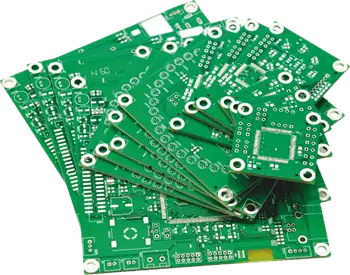
Circuit printing refers to additive manufacturing processes that can directly print the electrical traces and components onto substrate boards to construct functioning electronic circuits. This revolutionary technology promises to greatly simplify laying out custom printed circuit board (PCB) designs without relying on complex fabrication steps.
As hobbyists and startups push innovation boundaries with highly complex boards, circuit printing now offers an easier alternative to traditional PCB making methods. This article provides a comprehensive overview of various aspects of circuit printing including – suitable equipment, underlying printing process, key materials as well as overall costs.
Benefits of Circuit Printing
Here are some of the major advantages of adopting circuit printing:
- Allows printing functional electronics without harsh chemicals
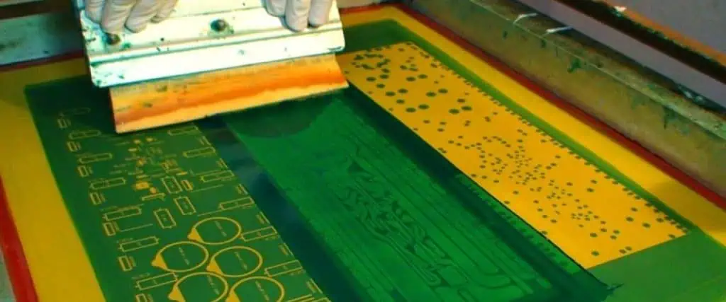
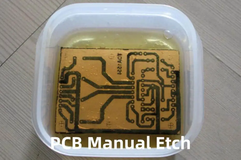
- Eliminates complex PCB fabrication steps like masking and etching
- Accommodates rapid design changes through easy file modification
- Enables embedding components within board itself
- Achieves finer trace resolution than commercial PCBs
- Allows printing unconventional substrate materials
- Simpler and cheaper than CNC milling or laser cutting
- Faster concept validation by instantly printing inventions
For rapid prototyping needs, circuit printers greatly simplify constructing new ideas.
Types of Circuit Printers

Various types of printing technologies allow additive formation of electrical circuit boards. The main circuit printing methods include:
Inkjet Printing
Uses piezoelectric print heads to jet tiny droplets of special conductive inks to draw circuit layouts on thin substrates.
Aerosol Jet Printing
Employs an aerodynamic focusing nozzle to atomize conductive ink into a dense aerosol spray which gets printed.
Nano-particle Jetting
Proprietary process utilizing gas flow to deposit metal nano-particle inks through an array of jet heads to print tracks.
Direct Ink Writing
Uses robotic 3D micro-extrusion of viscoelastic silver & graphene pastes to print free-standing wires without support.
Laser-Induced Forward Transfer
Lasers pulse to propel tiny volumes of conductive ink onto boards thus printing complex patterns with no masks.
Desktop sized circuit printers costing under $5000 target hobbyists and startups exploring innovative electronics ideas.
Circuit Printer Machine Considerations
When selecting circuit printers, key factors to evaluate include:
Print Resolution – Finer nozzle diameters allow more intricate circuits but reduce throughput. 100 μm lines are standard.
Print Speed – Print heads with higher jetting frequencies speed up printing larger boards. Minimal movement also boosts rates.
Supported Inks – Printers are usually optimized for certain proprietary conductive/resistive/dielectric ink chemistries.
Substrate Handling – Flatbed printers accommodate rigid boards up to 300mm x 500mm size while roll-to-roll printers suit flexible films.
Layer Registration – Precision board alignment for printing multi-layer circuits without shorting between layers.
Software Workflow – Seamless data interface from PCB design to printer interface to executing print runs quickly.
Cost – Desktop printers provide an affordable entry point but offer lower resolution and accuracy versus industrial solutions.
Analyzing application needs and production expectations guides appropriate printer selection.
Circuit Printing Process Overview
The typical circuit printing workflow involves:
1. Design – Creating required circuit layout in CAD software
2. File Conversion – Generating printer-specific file formats like Gerber/SVG/HPGL etc.
3. Substrate Loading – Mounting suitable board blank onto printer bed
4. Alignment – Precisely positioning substrate by optically detecting fiducials
5. Printing – Executing conductive ink deposition toolpaths
6. Drying – Using heaters or UV lights to quickly cure printed ink
7. Testing – Validating printed trace continuity and absence of shorts
8. Component Assembly – Mounting and soldering surface mount devices to complete circuit
This additive printing process revolutionizes laying out custom circuit boards.
Circuit Printing Materials

Specialized conductive and dielectric inks made using nano-particle metals and insulating polymers form the foundation for circuit printing.
Conductive Inks
Silver, copper or graphene based particle inks dispensed from cartridges serve to print the electrically functional traces and pads. Only 10-15% metal loading by weight is required for conductivity.
Dielectric Inks
Insulating acrylic-epoxy formulations precisely printed to encapsulate crossed-over traces or define soldermask areas prevent shorting while providing structural base.
Substrate
Materials like FR4, flexibilized PET/PC films, paper or textiles act as the foundational board blank to print circuits atop.
By developing custom inks tuned for stability and printability, a wide spectrum ofsubstrate materials can be transformed into functional electronics.
Design Rules for Printable Circuits
To effectively fabricate a circuit layout by printing, the PCB artwork must comply with certain constraints related to printhead capabilities, ink performance etc.
Follow these guidelines when designing circuits targeting additive printing:
1. Define minimum wire width: Static droplets constrain resolution so widths >= 100 microns print well.
2. Set spacing rules: Gap between adjacent traces should exceed nozzle diameter to prevent bridging shorts.
3. Minimize acute angles: Gradual bends aid continuous ink flow compared to tight angles risking interruptions.
4. Allow conductor overlaps: Intersecting traces should overprint each other slightly for reliable connections after curing.
5. Include fiducials: Printer camera detects board reference points like cross marks to align subsequent layers precisely.
6. Ink volume limits: Constrain total length x width of traces printed to avoid printhead clogging and downtime.
7. Validate DFM: Printer manufacturer design rule checks validate artwork suitability before actual printing.
Accounting for process-specific capabilities allows achieving high circuit print yields.
Layer Registration Accuracy

For reliable multi-layer circuit printing, accurate alignment between printed layers is vital to prevent electrical shorts. High precision is achieved through:
Precise Stages – Printer beds featuring linear drives, precision ground rails, and/or air bearings offer highly repeatable X-Y positioning.
Vision Systems – Onboard cameras and optical recognition algorithms provide accurate positional feedback for registration.
Fiducial Marks – Cross hair squares or circle center alignment patterns on each board layer serve as layer-to-layer image detection points.
Software Compensation – Any residual distortions are digitally compensated through warping printed image to match earlier layers.
Advanced printers provide 5-10 μm registration accuracy allowing dense multilayer circuits with traces pitched at 200-400 μm.
Sintering Process
Once printed, the deposited conductive ink traces require controlled heating to evaporate carriers, melt nano-particle metals and form connected solid tracks in a process called sintering.
Sintering drives off solvents and enhances inter-atomic diffusion bonding between particles to increase electrical conductivity. This fixation transforms printed patterns into functional traces.
Rapid photonic curing systems using high intensity pulsed light provide instantaneous selective sintering without degrading delicate substrates. Sintering occurs in seconds depending on volume to solidify prints.
Printing Cost Analysis
Evaluating the cost implications of adopting circuit printing involves:
Printer Equipment – Desktop printers for under $5000 target hobbyists while advanced inkjet printers suited for small-scale production can cost over $75,000.
Printed Electronics – Conductive inks price around $300 per liter while dielectric inks cost ~$200 for insulation and encapsulation.
Substrates – Base materials like FR4 blanks are $10-30 per square feet area depending on thickness. Flex PCB grades cost extra.
Ancillary Tools – Additional sintering systems, curing equipment, testing stations etc. entails further expenses.
Operator Labor – Prep time for file processing, setup, postprint steps require manual intervention so factor hourly rates.
For low volume printed electronics, equipment depreciation influences cost prominence while material and labor dominate for mass production economics.
Advantages over Conventional PCBs
Printed circuits offer many benefits compared to traditional rigid FR4 boards:
Simpler Fabrication – No repetitive masking, etching, stripping steps involved allowing faster prototyping.
Design Flexibility – Changing layouts only requires updated print file instead of regenerating entire fabrication process.
Substrate Versatility – Choice of foundation materials like textiles, polymers beyond just rigid laminates.
Environmental Sustainability – Process avoids using toxic chemicals required for conventional PCB manufacture.
Embedding Capability – Can directly print passive components like resistors/capacitors integrated into the board.
Superior High-Frequency Performance – Direct write circuits have smooth coplanar traces allowing high frequency operation.
Applications of Printed Electronics
The capabilities of printed electronics are enabling promising applications such as:
Wearable Devices – Directly printing circuits onto fabrics allows creating smart garments flexibly conforming to ergonomics.
Medical Sensors – Soft biosensors can monitor patient health parameters seamlessly when mounted directly on skin by printing.
Smart Packaging – In-mold electronics printing before injection molding plastic enclosures simplifies integrating circuits into products.
RFID Tags – Additively printing antenna and chip bonding lands greatly simplifies fabrication of wireless tags.
PE Textiles – Inkjet printing conductive patterns onto apparel can create flexible thin heating pads or illuminated clothing.
Automotive Displays – Low temperature deposition is ideal for directly printing polymer electronics onto curved surfaces inside cars.
Printing advancements offer electronics beyond mechanical PCB substrates to applications requiring form factor flexibility where conventional boards remain incompatible.
Limitations of Printed Electronics

While constantly improving, circuit printing technology still poses certain limitations presently:
Line Resolution – Printed traces remain thicker than photolithographic processes so circuits cannot miniaturize further.
Registration Accuracy – Overlay printing multiple ink layers precisely to prevent shorting between crossing conductors faces challenges.
Ink Stability – Ensuring shelf-life before particle settling as well as preventing printhead nozzle clogging need improvements.
Print Speeds – Additively generating intricate multilayer boards takes longer production time versus batch processing PCBs.
Conductor Quality – Achievable conductive ink resistivity still lags behind bulk copper tracks restricting high power applications.
Substrate Variety – Material compatibility still limits directly printing onto several advanced composites.
Further development of printing systems, inks and substrates continues to push boundaries lowering barriers to adoption.
Conclusion
Circuit printing promises to transform laying out even complicated electronics inventions by replacing tedious fabrication steps through direct material deposition. What used to rely on skilled technicians and days long process now gets simplified to instantly printing from CAD models inhouse. By merging printed electronics together with conventional components onto builder friendly substrates, innovators can bring product concepts to life faster and cheaper than ever before. Despite certain lingering limitations around ultimate miniaturization potential, registration needs and conductor quality, the ease-of-use and customization possible with printed circuits constitutes an invaluable asset during early development phases for enterprises and individual inventors alike. With global initiatives around environmentally progressive manufacturing also gaining prominence, it seems certain that printed electronics will continue making inroads providing simpler circuit foundations across an ever expanding slate of imaginative applications.
Frequently Asked Questions
Here are some common queries regarding circuit printing:
Q: What materials are used for printing substrates?
A: Paper, PET, PC and textiles allow low temperature deposition. Ceramic coated metal foils offer higher temperature stability. Composite boards also enable directly embedding printed electronics.
Q: What is achievable PCB line width resolution?
A: Most printers can achieve around 100 μm line width and 125 μm line spacing reliably. Ultra-precision systems approach 25 μm resolution but remain slower.
Q: Are printed circuits as conductive as copper boards?
A: Ink curing generates around 2-5x bulk resistivity relative to rolled copper so high power density boards still favor etched metal tracks today.
Q: Can components be directly printed onto boards?
A: Modern ink chemistries allow co-printing simple resistors, capacitors, antennas alongside conductors in a single pass but traditional SMD devices still need manual attach.
Q: How accurate is layer-to-layer registration?
A: Advanced Industrial printers ensure registration accuracy within 5-10 μm allowing reliable interlayer interconnections at 200+ μm pitch. Hobby printers remain ~50 μm.
