How To Choose the Right Thickness for Your PCB Prototype

Thick PCB

Selecting the appropriate thickness for your Printed Circuit Board (PCB) prototype is a crucial decision that can significantly impact the performance, durability, and overall success of your electronic project. This comprehensive guide will walk you through the various factors to consider when determining the ideal PCB thickness for your specific application.

Understanding PCB Thickness

What is PCB Thickness?

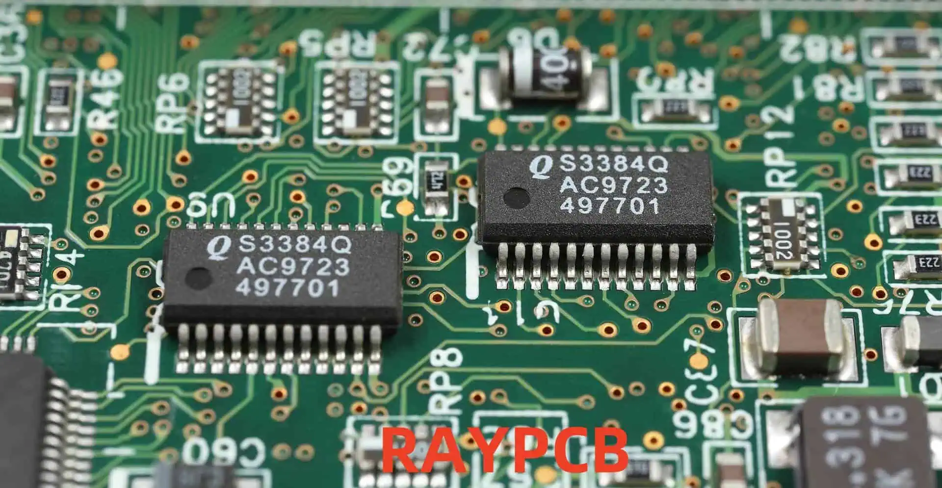
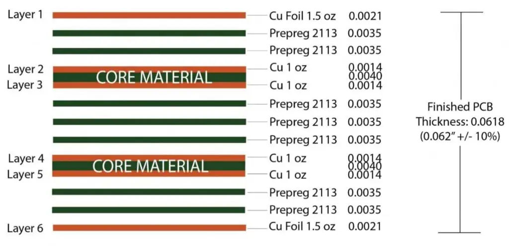
PCB thickness refers to the overall depth of the circuit board, including all layers of substrate, copper, and other materials used in its construction.

Standard PCB Thicknesses

Thickness Ranges

While custom thicknesses are available, most PCB manufacturers offer standard options to choose from:

Thickness (mm) Thickness (inches) Common Applications
0.4 mm 0.016″ Flexible PCBs, wearables
0.8 mm 0.031″ Mobile devices, thin electronics
1.6 mm 0.062″ Standard thickness for most applications
2.4 mm 0.093″ High-power applications, rugged devices
3.2 mm 0.125″ Industrial equipment, power supplies

Factors Influencing PCB Thickness Choice

1. Application Requirements

Consumer Electronics

Consumer electronics often require thinner PCBs to achieve compact designs.

Considerations for Consumer Electronics PCBs:

Industrial Applications

Industrial PCBs typically need to be more robust and may require thicker boards.

Factors for Industrial PCB Thickness:
  • Vibration resistance
  • Temperature extremes
  • Exposure to harsh environments
  • Long-term reliability

2. Mechanical Strength

The thickness of a PCB directly affects its mechanical strength and ability to withstand physical stress.

Relationship Between Thickness and Strength

Thickness Relative Strength Suitable Applications
Thin (<1.0 mm) Low Flexible electronics, space-constrained devices
Medium (1.0-2.0 mm) Moderate Most consumer electronics, general-purpose devices
Thick (>2.0 mm) High Industrial equipment, high-stress environments

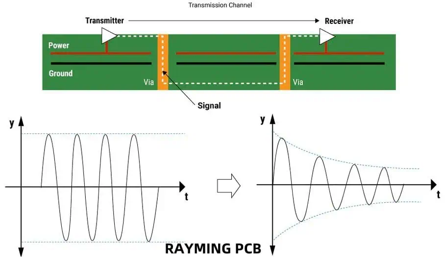
3. Electrical Performance

PCB thickness can impact the electrical characteristics of your circuit.

Electrical Considerations:

  • Impedance control
  • Signal integrity
  • EMI/EMC performance
  • Power handling capacity

4. Thermal Management

The ability of a PCB to dissipate heat is partly dependent on its thickness.

Thermal Factors:

  • Heat-generating components
  • Copper weight and distribution
  • Thermal vias and planes
  • Ambient operating temperature

5. Component Compatibility

The choice of components can influence the required PCB thickness.

Component-Related Factors:

6. Manufacturing Constraints

PCB thickness can affect the manufacturing process and associated costs.

Manufacturing Considerations:

  • Minimum feature size and aspect ratio
  • Via technology (through-hole, blind, buried)
  • Layer count and stack-up design
  • Production volume and cost

Selecting the Right Thickness for Different PCB Types

Single-Layer PCBs

Single-layer PCBs are the simplest type and are often used in basic electronic devices.

Recommended Thicknesses for Single-Layer PCBs:

  • 0.8 mm – 1.6 mm for most applications
  • Thinner (0.4 mm – 0.6 mm) for flexible or ultra-compact designs
  • Thicker (2.4 mm+) for high-power or rugged applications

Double-Layer PCBs

Double-layer PCBs offer more design flexibility and are commonly used in various electronic devices.

Typical Thicknesses for Double-Layer PCBs:

  • 1.6 mm is the most common thickness
  • 0.8 mm – 1.2 mm for space-constrained applications
  • 2.4 mm for increased durability or thermal management
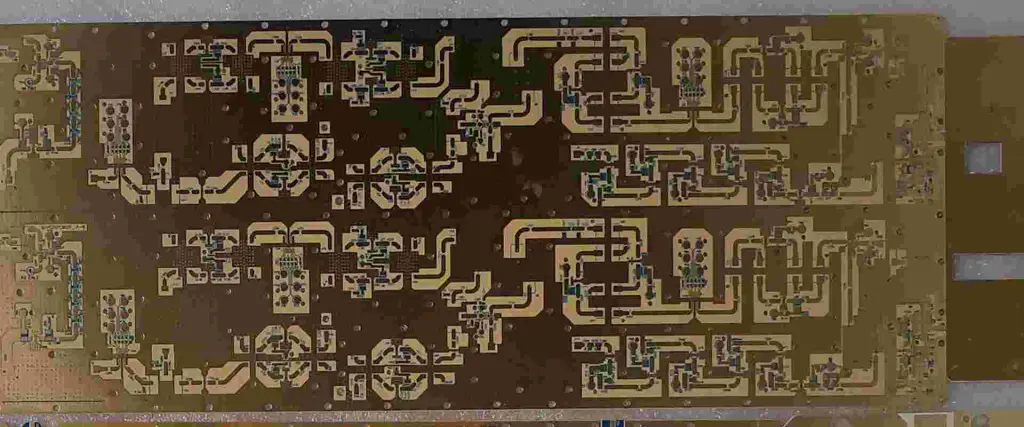
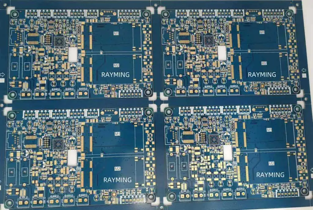
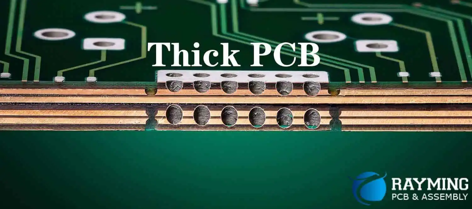
Multi-Layer PCBs

Multi-layer PCBs are used in complex electronic systems and require careful consideration of thickness.

Thickness Guidelines for Multi-Layer PCBs:

Layer Count Recommended Thickness Range (mm)
4 – 6 layers 1.6 – 2.4 mm
8 – 10 layers 1.6 – 3.2 mm
12+ layers 2.4 – 3.2 mm or custom

Special Considerations for Specific Applications

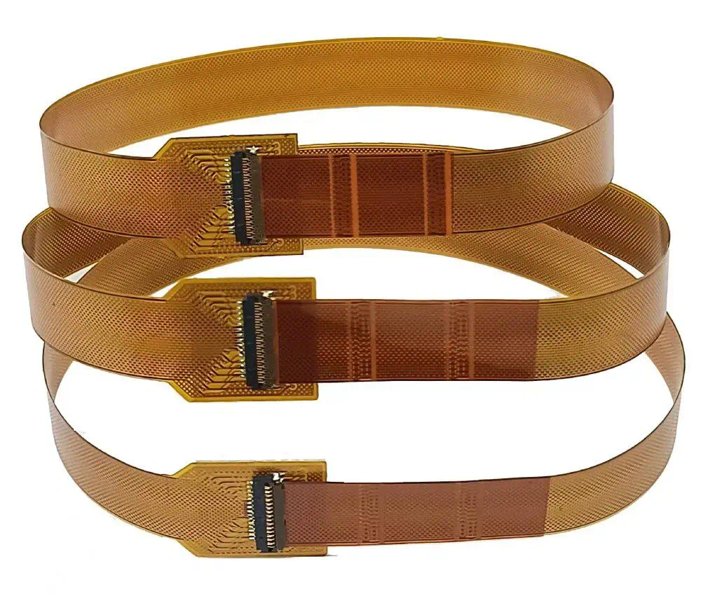
Flex and Rigid-Flex PCBs

Flex and rigid-flex PCBs require special attention to thickness for optimal performance.

Flex PCB Thickness Considerations:

flex PCB thickness
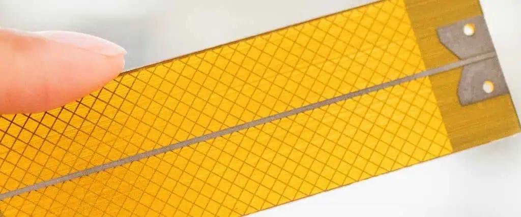
  • Ultra-thin (0.1 mm – 0.2 mm) for maximum flexibility
  • 0.3 mm – 0.6 mm for standard flex applications
  • Consider the number of flex cycles required

Rigid-Flex PCB Thickness Factors:

  • Thickness transition between rigid and flex sections
  • Overall stack-up design
  • Bend radius requirements
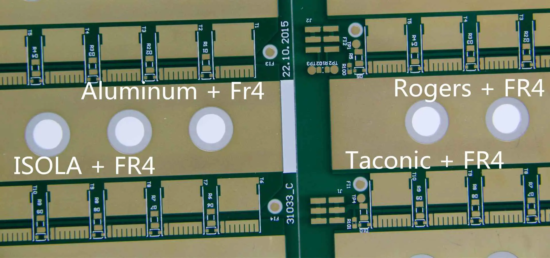
High-Frequency PCBs

High-frequency applications demand precise control over PCB thickness for optimal signal integrity.

High-Frequency PCB Thickness Factors:

  • Dielectric constant of substrate materials
  • Impedance control requirements
  • Skin effect considerations
  • Minimize thickness variations for consistent performance

Power Electronics PCBs

Power electronics often require thicker PCBs to handle high currents and thermal loads.

Power PCB Thickness Considerations:

  • Copper weight and current-carrying capacity
  • Thermal management requirements
  • Voltage isolation needs
  • Mechanical stress from heavy components

PCB Thickness and Cost Considerations

The thickness of your PCB can impact the overall cost of your project.

Cost Factors Related to PCB Thickness:

  1. Material usage
  2. Manufacturing complexity
  3. Yield rates
  4. Shipping and handling

Cost Impact of PCB Thickness

Thickness Range Relative Cost Cost Factors
Thin (<1.0 mm) Higher Specialized materials, handling challenges
Standard (1.0-2.0 mm) Baseline Most economical for general purposes
Thick (>2.0 mm) Higher Increased material usage, longer processing times

Best Practices for Choosing PCB Thickness

Follow these best practices to ensure you select the optimal thickness for your PCB prototype:

  1. Define Your Requirements: Clearly outline your project’s electrical, mechanical, and environmental needs.
  2. Consider Future Needs: Allow for potential upgrades or modifications in your thickness selection.
  3. Consult with Manufacturers: Leverage the expertise of PCB fabrication houses for guidance.
  4. Prototype Iterations: Test different thicknesses if possible to find the optimal balance of performance and cost.
  5. Balance Trade-offs: Weigh the pros and cons of different thicknesses against your project goals.
  6. Stay Standard When Possible: Use standard thicknesses unless your application absolutely requires a custom option.
  7. Think Holistically: Consider how thickness affects all aspects of your design, from electrical performance to manufacturing.

Emerging Trends in PCB Thickness

Stay ahead of the curve by considering these emerging trends in PCB thickness:

  1. Ultra-Thin PCBs: Advancements in materials and manufacturing are enabling ever-thinner PCBs for compact devices.
  2. Embedded Components: Integrating components within PCB layers is changing thickness requirements.
  3. 3D Printed Electronics: Additive manufacturing is allowing for more precise control over PCB thickness and structure.
  4. High-Density Interconnect (HDI): HDI technology is pushing the boundaries of thin, complex PCB designs.
  5. Advanced Materials: New substrate materials are offering improved performance at various thicknesses.

Frequently Asked Questions (FAQ)

1. How does PCB thickness affect signal integrity?

PCB thickness can significantly impact signal integrity, especially in high-speed or high-frequency applications. Thicker boards generally provide better signal integrity due to reduced crosstalk and improved impedance control. However, very thick boards can lead to longer via lengths, which may introduce signal degradation. The key is to find the right balance based on your specific application requirements, considering factors such as trace width, spacing, and layer stack-up design.

2. Can I use different thicknesses within the same PCB design?

Yes, it’s possible to use different thicknesses within the same PCB design, especially in rigid-flex PCBs. This approach, known as hybrid or step PCB design, allows for optimized thickness in different areas of the board. However, it requires careful planning and may increase manufacturing complexity and cost. Always consult with your PCB manufacturer to ensure feasibility and discuss any potential challenges.

3. How do I determine the minimum thickness for my PCB?

To determine the minimum thickness for your PCB, consider the following factors:

  1. Mechanical strength requirements
  2. Component types and sizes (especially for through-hole components)
  3. Electrical performance needs (e.g., impedance control, current-carrying capacity)
  4. Thermal management considerations
  5. Manufacturing limitations (e.g., aspect ratio for drilled holes)
  6. Environmental factors (e.g., vibration, temperature extremes)

Start with the thinnest standard thickness that meets all your requirements, then adjust as necessary based on prototyping and testing results.

4. What are the challenges associated with very thick PCBs?

While thick PCBs offer advantages in terms of strength and thermal management, they also present several challenges:

  1. Increased material costs
  2. Longer manufacturing times, especially for drilling and plating processes
  3. Difficulties in achieving high-aspect-ratio vias
  4. Potential for increased weight, which may be undesirable in some applications
  5. Challenges in creating uniform plating in through-holes
  6. Possible limitations in component selection due to lead length requirements

Always weigh these challenges against the benefits when considering very thick PCBs for your application.

5. How does PCB thickness affect the overall weight of my device?

PCB thickness directly impacts the weight of your device. As a general rule, doubling the thickness of a PCB will approximately double its weight, assuming the same board dimensions and materials. Here’s a rough guide for estimating PCB weight based on thickness (using standard FR-4 material):

Thickness (mm) Approximate Weight (g/cmยฒ)
0.8 mm 0.15 g/cmยฒ
1.6 mm 0.30 g/cmยฒ
2.4 mm 0.45 g/cmยฒ
3.2 mm 0.60 g/cmยฒ

Remember that these are approximate values and can vary based on copper weight, layer count, and specific materials used. For weight-sensitive applications, consider using thinner PCBs or exploring lightweight substrate materials.

In conclusion, choosing the right thickness for your PCB prototype is a critical decision that requires careful consideration of various factors. By understanding the impact of thickness on performance, manufacturability, and cost, you can make an informed decision that optimizes your PCB design for its intended application. Remember to consult with PCB manufacturers and consider prototyping different options to find the ideal thickness for your specific needs.

Easy PCB Assembly Tips and Tricks That Will Help Any Beginner

Printed Circuit Board (PCB) assembly is a crucial skill for anyone interested in electronics. Whether you’re a hobbyist, a student, or an aspiring professional, mastering PCB assembly can open up a world of possibilities for creating your own electronic projects. This article will provide you with essential tips and tricks to make your PCB assembly journey smoother and more enjoyable.

Understanding PCB Basics

Before diving into assembly techniques, it’s important to understand the basics of PCBs.

What is a PCB?

A Printed Circuit Board (PCB) is a board that connects electronic components using conductive tracks, pads, and other features etched from copper sheets laminated onto a non-conductive substrate.

Components of a PCB

PCBs consist of several key elements:

  1. Substrate
  2. Copper layers
  3. Solder mask
  4. Silkscreen
  5. Pads and vias
  6. Traces

Types of PCBs

PCB TypeDescriptionCommon Applications
Single-sidedOne copper layerSimple electronics, calculators
Double-sidedTwo copper layersPower supplies, amplifiers
Multi-layerThree or more copper layersSmartphones, computers
RigidStandard inflexible boardMost electronic devices
FlexFlexible substrateWearables, compact devices
Rigid-flexCombination of rigid and flexAerospace, medical devices

Essential Tools for PCB Assembly

Having the right tools is crucial for successful PCB assembly. Here’s a list of essential tools:

Soldering Equipment

  1. Soldering iron
  2. Soldering station
  3. Solder wire
  4. Flux
  5. Desoldering pump or wick

Hand Tools

  1. Needle-nose pliers
  2. Wire cutters
  3. Tweezers
  4. Magnifying glass or loupe
  5. Multimeter

Safety Equipment

  1. Safety glasses
  2. Fume extractor
  3. Heat-resistant mat
  4. Anti-static wrist strap

Optional but Helpful Tools

  1. Hot air rework station
  2. Microscope
  3. PCB holder or vise
  4. Solder paste dispenser

Preparing for PCB Assembly

SMT soldering Process

Proper preparation is key to successful PCB assembly. Follow these steps to ensure you’re ready to begin:

1. Gather All Necessary Components

Create a bill of materials (BOM) and ensure you have all required components before starting.

2. Organize Your Workspace

Set up a clean, well-lit area with all your tools within reach.

3. Review the PCB Design

Familiarize yourself with the PCB layout and component placement.

4. Check for Any Design Errors

Double-check the PCB design for any mistakes before beginning assembly.

5. Clean the PCB

Use isopropyl alcohol to clean the PCB surface before soldering.

PCB Assembly Techniques

There are two main techniques for PCB assembly: through-hole and surface mount. We’ll cover both methods in detail.

Through-Hole Assembly

Through-hole assembly involves inserting component leads through holes in the PCB and soldering them on the opposite side.

Steps for Through-Hole Assembly

  1. Insert components
  2. Bend leads slightly to hold components in place
  3. Flip the board
  4. Solder leads
  5. Trim excess lead length

Tips for Through-Hole Soldering

  1. Heat both the pad and the lead
  2. Apply solder to the junction, not the iron tip
  3. Create a small solder fillet around the lead
  4. Avoid overheating components

Surface Mount Assembly

Surface Mount Technology (SMT) involves soldering components directly onto the surface of the PCB.

Steps for Surface Mount Assembly

  1. Apply solder paste to pads
  2. Place components using tweezers
  3. Reflow solder using a hot air station or reflow oven
  4. Inspect and touch up as needed

Tips for Surface Mount Soldering

  1. Use a stencil for applying solder paste
  2. Practice component placement with tweezers
  3. Start with larger components and work your way to smaller ones
  4. Use flux to improve solder flow

Common PCB Assembly Mistakes and How to Avoid Them

Being aware of common mistakes can help you avoid them in your own projects.

1. Incorrect Component Orientation

Always double-check component polarity and orientation before soldering.

2. Cold Solder Joints

Ensure proper heating of both the pad and component lead for a good solder joint.

3. Solder Bridges

Use the appropriate amount of solder and clean your iron tip regularly to prevent bridges.

4. Overheating Components

Be mindful of heat-sensitive components and use heat sinks when necessary.

5. Poor Flux Removal

Clean the PCB thoroughly after soldering to remove flux residue.

Advanced PCB Assembly Techniques

smt pcb assembly machinesmt pcb assembly machine

Once you’ve mastered the basics, you can move on to more advanced techniques.

1. BGA and QFN Soldering

Ball Grid Array (BGA) and Quad Flat No-lead (QFN) packages require specialized equipment and techniques.

2. Reflow Soldering

Using a reflow oven or hot plate for precise temperature control during SMT assembly.

3. Wave Soldering

Automated soldering technique for through-hole components in high-volume production.

4. Mixed Technology Assembly

Combining through-hole and surface mount components on the same board.

Troubleshooting and Rework

Even with careful assembly, issues may arise. Here are some troubleshooting tips:

Visual Inspection

Use a magnifying glass or microscope to check for:

  1. Solder bridges
  2. Missing solder joints
  3. Incorrect component placement
  4. Damaged components

Electrical Testing

Use a multimeter to check for:

  1. Continuity
  2. Proper voltage levels
  3. Resistance measurements

Common Rework Techniques

IssueRework Technique
Solder bridgeUse desoldering wick to remove excess solder
Cold jointReflow the solder joint with fresh solder
Misaligned componentUse hot air to remove and reposition
Damaged padCreate a solder bridge or use wire to bypass

Best Practices for PCB Assembly

Follow these best practices to improve your PCB assembly skills:

1. Work in a Clean Environment

Minimize dust and contaminants in your workspace.

2. Use Quality Tools and Materials

Invest in good-quality soldering equipment and components.

3. Practice Proper ESD Protection

Use an anti-static wrist strap and mat to prevent damage to sensitive components.

4. Take Breaks and Stay Focused

PCB assembly requires concentration. Take regular breaks to maintain focus.

5. Document Your Work

Keep notes on your assembly process for future reference.

6. Continual Learning

Stay updated on new techniques and technologies in PCB assembly.

Environmental Considerations in PCB Assembly

As an electronics enthusiast, it’s important to consider the environmental impact of your hobby.

1. Use Lead-Free Solder

Opt for lead-free solder to reduce environmental hazards.

2. Proper Disposal of Electronic Waste

Recycle old PCBs and components through appropriate e-waste channels.

3. Energy Efficiency

Use energy-efficient soldering equipment and turn off tools when not in use.

4. Minimize Chemical Use

Use flux and cleaning agents sparingly and opt for environmentally friendly options when possible.

Future Trends in PCB Assembly

Stay ahead of the curve by familiarizing yourself with emerging trends in PCB assembly:

1. Automated Assembly

Increasing use of pick-and-place machines and automated soldering systems.

2. 3D Printed Electronics

Integration of 3D printing technology with PCB manufacturing.

3. Flexible and Stretchable PCBs

Development of PCBs that can bend or stretch for wearable electronics.

4. Embedded Components

Incorporating components within the PCB layers for increased density.

5. AI-Assisted Design and Assembly

Leveraging artificial intelligence for optimized PCB design and assembly processes.

Frequently Asked Questions (FAQ)

1. What’s the difference between through-hole and surface mount assembly?

Through-hole assembly involves inserting component leads through holes in the PCB and soldering them on the opposite side. Surface mount assembly involves soldering components directly onto the surface of the PCB. Through-hole is generally easier for beginners but takes up more space, while surface mount allows for higher component density and is more commonly used in modern electronics.

2. How do I choose the right soldering iron temperature?

The correct soldering iron temperature depends on the type of solder you’re using and the components you’re working with. As a general rule:

  • For lead-based solder: 300-330ยฐC (572-626ยฐF)
  • For lead-free solder: 350-370ยฐC (662-698ยฐF) Always start at a lower temperature and increase as needed to achieve good solder flow without damaging components.

3. How can I prevent solder bridges?

To prevent solder bridges:

  1. Use the appropriate amount of solder
  2. Keep your soldering iron tip clean
  3. Use flux to improve solder flow
  4. Practice proper soldering technique
  5. Use a finer soldering iron tip for closely spaced pads If bridges do occur, use desoldering wick or a solder sucker to remove excess solder.

4. What should I do if I accidentally damage a pad on the PCB?

If you damage a pad:

  1. Clean the area thoroughly
  2. If possible, scrape away the solder mask to expose nearby traces
  3. Use a small wire to create a jumper from the component lead to the exposed trace
  4. Solder the wire in place
  5. Use epoxy to secure the repair if needed For more severe damage, you may need to use a PCB repair kit or consider replacing the board.

5. How important is flux in PCB assembly?

Flux is crucial in PCB assembly as it:

  1. Removes oxides from the metal surfaces
  2. Improves solder flow and wetting
  3. Helps create stronger solder joints
  4. Prevents solder balls and bridges Always use flux when soldering, either as a separate product or within your solder wire. Remember to clean flux residue after soldering to prevent corrosion and electrical issues.

In conclusion, PCB assembly is a valuable skill that combines technical knowledge with hands-on practice. By following these tips and tricks, beginners can build a strong foundation for successful PCB assembly. Remember that patience and persistence are key โ€“ with practice, you’ll soon be creating professional-quality PCB assemblies for your electronics projects.

6 Amazing PCB Facts You Might Not Know

Printed Circuit Boards (PCBs) are the unsung heroes of modern electronics. These intricate networks of conductors and components form the backbone of nearly every electronic device we use today. While most people are familiar with the green boards found inside computers and smartphones, there’s much more to PCBs than meets the eye. In this article, we’ll explore six fascinating facts about PCBs that might surprise even the most tech-savvy individuals.

1. PCBs Have a Rich History Dating Back to World War II

The Birth of Modern Electronics

The story of PCBs begins in the early 20th century, but it was during World War II that they truly came into their own. The need for reliable and compact electronic systems in military equipment drove rapid innovation in circuit board technology.

From Point-to-Point to Printed Circuits

Before PCBs, electronic components were connected using point-to-point construction. This method was time-consuming, prone to errors, and resulted in bulky, unreliable devices. The development of PCBs revolutionized electronics manufacturing by providing a more efficient and reliable alternative.

Key Milestones in PCB History
ColorCommon UsesCharacteristics
GreenGeneral electronicsTraditional, most common
BlueAerospace, medical devicesHigh contrast for inspection
RedTelecommunicationsHeat resistant
BlackAudio equipmentReduces light reflection
WhiteLED applicationsEnhances light reflection
YellowAutomotiveHigh visibility for safety
PurpleMilitary and defenseSpecific military standards

The evolution of PCBs from wartime necessity to commercial ubiquity is a testament to their versatility and importance in modern electronics.

2. PCBs Come in a Rainbow of Colors

Rogers RO4835 PCB

Beyond the Traditional Green

When most people think of PCBs, they picture the iconic green boards found in many electronic devices. However, PCBs actually come in a wide variety of colors, each serving a specific purpose or adhering to certain industry standards.

The Colorful World of PCBs

CharacteristicRigid PCBsFlexible PCBsStretchable PCBs
Base MaterialFR-4, ceramicPolyimide, polyesterElastomers, silicone
FlexibilityNoneCan bend and foldCan elongate
DurabilityHighMedium to HighMedium
CostLowerHigherHighest
Space EfficiencyLowHighVery High
WeightHeavierLighterLightest
Application RangeWideSpecializedHighly specialized

The Significance of PCB Colors

While the color of a PCB doesn’t directly affect its electrical performance, it can serve several important functions:

  1. Identification: Different colors can help manufacturers quickly identify board types or revisions.
  2. Inspection: Some colors provide better contrast, making visual inspection easier.
  3. Thermal Management: Certain colors can help with heat dissipation or retention.
  4. Aesthetics: In consumer electronics, PCB color can be chosen to match product design.
  5. Industry Standards: Some industries have color preferences or requirements for PCBs.

Understanding the diverse palette of PCB colors reveals the thoughtful design considerations that go into even the most minute aspects of electronic manufacturing.

3. PCBs Can Be Flexible and Even Stretchable

Breaking the Rigid Mold

While traditional PCBs are rigid, technological advancements have led to the development of flexible and even stretchable PCBs. These innovations are opening up new possibilities in electronics design and application.

Flexible PCBs

Flexible PCBs (or flex PCBs) are made using flexible base materials like polyimide or polyester films. They can bend, fold, and conform to various shapes, making them ideal for applications where space is at a premium or where the PCB needs to fit into unconventional spaces.

Applications of Flexible PCBs
  1. Smartphones and tablets
  2. Wearable technology
  3. Medical devices (e.g., pacemakers)
  4. Automotive electronics
  5. Aerospace systems

Stretchable PCBs

Taking flexibility even further, stretchable PCBs can elongate and return to their original shape without losing functionality. This emerging technology is still in its early stages but shows great promise for future applications.

Potential Uses for Stretchable PCBs
  1. Smart clothing
  2. Biomedical implants
  3. Soft robotics
  4. Human-machine interfaces
  5. Structural health monitoring

Comparison: Rigid vs. Flexible vs. Stretchable PCBs

EraTypical Maximum LayersCommon Applications
1960s4 layersEarly computers
1980s8-12 layersPersonal computers
2000s20-30 layersServers, high-end electronics
2020s50+ layersSupercomputers, advanced telecommunications

The development of flexible and stretchable PCBs demonstrates the ongoing innovation in the field of electronics, pushing the boundaries of what’s possible in device design and functionality.

4. PCBs Can Have Up to 50+ Layers

The World of Multilayer PCBs

While simple electronic devices might use single or double-layer PCBs, complex systems often require multilayer boards. These PCBs consist of multiple layers of conductive material separated by insulating layers, allowing for incredibly dense and complex circuitry.

The Evolution of PCB Layers

EraTypical Maximum LayersCommon Applications
1960s4 layersEarly computers
1980s8-12 layersPersonal computers
2000s20-30 layersServers, high-end electronics
2020s50+ layersSupercomputers, advanced telecommunications

Benefits of Multilayer PCBs

  1. Increased Circuit Density: More layers allow for more components and connections in a smaller area.
  2. Improved Signal Integrity: Dedicated ground and power planes reduce noise and interference.
  3. Better EMI Shielding: Multiple layers can provide better protection against electromagnetic interference.
  4. Enhanced Thermal Management: More layers can help distribute and dissipate heat more effectively.
  5. Reduced Size and Weight: Complex circuits can be packed into smaller, lighter boards.

Challenges of High Layer Count PCBs

While the benefits of multilayer PCBs are significant, they also present unique challenges:

  1. Manufacturing Complexity: Each additional layer increases the difficulty and cost of production.
  2. Signal Propagation: Signals traveling through many layers can experience delays and distortion.
  3. Thermal Management: Heat dissipation becomes more complex with tightly packed layers.
  4. Testing and Troubleshooting: Identifying issues in deeply buried layers can be challenging.

Despite these challenges, the demand for ever-more complex and compact electronic devices continues to drive innovation in multilayer PCB technology.

5. PCBs Can Be Manufactured with Embedded Components

Revolutionizing PCB Design

Embedded component technology is a cutting-edge approach to PCB manufacturing where components are integrated directly into the inner layers of the board. This technique represents a significant leap forward in electronics miniaturization and performance optimization.

Types of Embedded Components

  1. Active Components: Transistors, ICs, LEDs
  2. Passive Components: Resistors, capacitors, inductors

Advantages of Embedded Component Technology

AdvantageDescription
Size ReductionComponents embedded within layers save surface space
Improved PerformanceShorter connection paths reduce signal delays and interference
Enhanced ReliabilityProtected components are less susceptible to environmental factors
Better Thermal ManagementImproved heat distribution throughout the board
Increased Design FlexibilityAllows for more creative and efficient circuit layouts

Challenges and Considerations

While embedded component technology offers numerous benefits, it also presents some challenges:

  1. Manufacturing Complexity: Requires specialized equipment and processes
  2. Cost: Initially more expensive than traditional PCB manufacturing
  3. Repairability: Embedded components are difficult or impossible to replace
  4. Testing: Requires advanced techniques to ensure proper functionality

Despite these challenges, embedded component technology is gaining traction in industries where size, performance, and reliability are critical, such as aerospace, medical devices, and high-end consumer electronics.

6. PCBs Can Be Manufactured Using 3D Printing Technology

The Future of PCB Prototyping and Production

3D printing, also known as additive manufacturing, is revolutionizing many industries, and PCB manufacturing is no exception. While traditional PCB manufacturing methods remain dominant for large-scale production, 3D printing offers exciting possibilities for rapid prototyping and small-batch production.

3D Printed PCB Manufacturing Methods

  1. Fused Deposition Modeling (FDM): Layering conductive and non-conductive materials
  2. Stereolithography (SLA): Using photosensitive resins and conductive inks
  3. Aerosol Jet Printing: Depositing nano-particle inks for fine-pitch circuits

Comparison: Traditional vs. 3D Printed PCBs

AspectTraditional PCBs3D Printed PCBs
Production SpeedSlower for prototypesRapid prototyping
Minimum Feature SizeVery small (0.1mm or less)Larger (0.5mm typical)
Material OptionsLimitedDiverse, including flexible materials
Cost for Small BatchesHigherLower
Environmental ImpactHigher (chemical processes)Lower (less waste)
ComplexityHighMedium to High
ScalabilityExcellentLimited

Applications and Future Prospects

3D printed PCBs are particularly useful in:

  1. Rapid prototyping for product development
  2. Custom electronics for research and education
  3. Small-batch production for specialized devices
  4. Creating unique form factors and flexible circuits

As 3D printing technology continues to advance, we can expect improvements in resolution, material properties, and production speed. This could lead to more widespread adoption of 3D printed PCBs in various industries, potentially revolutionizing the way we design and manufacture electronic devices.

Frequently Asked Questions (FAQ)

1. What does PCB stand for, and what is its primary function?

PCB stands for Printed Circuit Board. Its primary function is to mechanically support and electrically connect electronic components using conductive tracks, pads, and other features etched from copper sheets laminated onto a non-conductive substrate.

2. How long does it typically take to manufacture a PCB?

The time to manufacture a PCB can vary widely depending on complexity, number of layers, and production volume. For simple boards, it can take as little as 24 hours for prototypes. More complex multilayer boards or large production runs can take several weeks.

3. Are PCBs recyclable?

Yes, PCBs are recyclable, but the process is complex due to the variety of materials used in their construction. Specialized e-waste recycling facilities can extract valuable metals like copper and gold from PCBs while safely disposing of potentially harmful substances.

4. What’s the difference between a PCB and a PCBA?

A PCB (Printed Circuit Board) is the bare board with conductive tracks but no components. A PCBA (Printed Circuit Board Assembly) is a PCB that has had components soldered onto it, creating a functional electronic circuit.

5. Can PCBs be repaired if damaged?

In many cases, PCBs can be repaired if damaged. Common repairs include replacing damaged components, repairing broken traces, and fixing solder joints. However, the feasibility and cost-effectiveness of repair depend on the extent of the damage and the complexity of the board.

In conclusion, PCBs are fascinating pieces of technology that continue to evolve and shape the world of electronics. From their colorful appearances to their flexible forms and embedded components, PCBs are far more diverse and complex than many people realize. As technology advances, we can expect to see even more innovations in PCB design and manufacturing, further pushing the boundaries of what’s possible in electronic devices.

A Brief History of Printed Circuit Boards

ROGERS + FR4 PCB

Printed Circuit Boards (PCBs) are the backbone of modern electronics, serving as the foundation for countless devices we use daily. From smartphones to satellites, PCBs have revolutionized the way we design, manufacture, and use electronic equipment. This article will take you on a journey through time, exploring the fascinating history of PCBs from their humble beginnings to their current state-of-the-art applications.

The Early Days: Pre-PCB Era

Point-to-Point Construction

Before the advent of PCBs, electronic devices were assembled using a method called point-to-point construction. This technique involved connecting components directly to each other or to terminal strips using wires.

Challenges of Point-to-Point Construction

  1. Time-consuming assembly process
  2. Prone to wiring errors
  3. Difficult to repair and maintain
  4. Limited scalability for complex circuits
  5. Bulky and heavy designs

The Need for a Better Solution

As electronic devices became more complex, the limitations of point-to-point construction became increasingly apparent. Engineers and inventors began searching for more efficient and reliable methods to connect electronic components.

The Birth of Printed Circuit Boards

100-layer-PCB-circuit-board

Early Concepts and Patents

The concept of printed circuits dates back to the early 20th century. Several inventors contributed to the development of what would eventually become the modern PCB.

Key Early Patents

YearInventorContribution
1903Albert HansonPatented flat foil conductors on an insulating board
1904Thomas EdisonExperimented with chemical methods of plating conductors onto linen paper
1913Arthur BerryPatented a print-and-etch method for producing circuit patterns
1925Charles DucasPatented a method of creating an electrical path directly on an insulated surface

The Breakthrough: Paul Eisler’s Invention

While these early patents laid the groundwork, it was Paul Eisler who is widely credited with inventing the modern printed circuit board in 1936.

Paul Eisler’s Contribution

  • Developed the PCB while working on a radio set in England
  • Initially used the technology to build a radio for personal use
  • Filed a patent for his invention in 1943

World War II: The Catalyst for PCB Development

Military Applications

World War II played a crucial role in accelerating the development and adoption of PCB technology.

PCBs in Wartime Technology

  1. Proximity Fuses: PCBs were used in proximity fuses for anti-aircraft shells
  2. Radio and Communication Equipment: Compact and reliable circuits were essential for military communication
  3. Radar Systems: PCBs enabled the miniaturization of radar equipment

Post-War Commercialization

After the war, the U.S. government released the technology for commercial use, paving the way for widespread adoption in consumer electronics.

The 1950s-1960s: PCB Technology Takes Off

Transition to Commercial Use

The 1950s saw a rapid increase in PCB use across various industries, particularly in consumer electronics.

Milestones in Commercial PCB Adoption

YearEvent
1947First commercial PCB produced in the United States
1948U.S. Army releases PCB technology for commercial use
1956Photoengraving process developed, allowing for more complex PCB designs
1960First fully automated PCB assembly line introduced

Technological Advancements

The 1960s brought significant improvements in PCB manufacturing techniques and materials.

Key Advancements

  1. Introduction of multi-layer PCBs
  2. Development of plated-through holes
  3. Improvement in base materials (e.g., FR-4 glass-reinforced epoxy laminate)
  4. Advancements in etching and plating processes

The 1970s-1980s: The PC Revolution

PCBs in Personal Computing

The rise of personal computers in the 1970s and 1980s dramatically increased demand for PCBs and drove further innovation in the field.

Notable PCB-Driven Computer Advancements

  1. 1971: Intel 4004, the first commercially available microprocessor
  2. 1977: Apple II, one of the first successful mass-produced microcomputers
  3. 1981: IBM PC, which set the standard for personal computers

Surface Mount Technology (SMT)

The introduction of surface mount technology in the 1980s marked a significant leap forward in PCB design and manufacturing.

Advantages of SMT

  1. Increased component density
  2. Reduced board size and weight
  3. Improved electrical performance
  4. Lower production costs
  5. Enhanced reliability

The 1990s-2000s: Miniaturization and Complexity

Shrinking Form Factors

As consumer electronics became smaller and more portable, PCB designers faced new challenges in miniaturization.

Miniaturization Techniques

  1. High-Density Interconnect (HDI) PCBs
  2. Micro via technology
  3. Buried and blind vias
  4. Flex and rigid-flex PCBs

Increasing Complexity

The demand for more powerful and feature-rich electronics led to increasingly complex PCB designs.

Advancements in PCB Complexity

  1. Increase in layer count (up to 30+ layers)
  2. Finer trace widths and spaces
  3. Advanced materials for high-speed and high-frequency applications
  4. Embedded passive and active components

The 2010s-Present: Smart Manufacturing and Industry 4.0

PCB Design and Manufacturing in the Digital Age

The past decade has seen a shift towards smart manufacturing and Industry 4.0 principles in PCB production.

Key Technologies in Modern PCB Manufacturing

  1. Computer-Aided Design (CAD) and simulation tools
  2. Automated Optical Inspection (AOI)
  3. 3D printing for rapid prototyping
  4. Artificial Intelligence and Machine Learning for design optimization

Emerging Trends in PCB Technology

As we move further into the 21st century, several exciting trends are shaping the future of PCB technology.

Current and Future PCB Trends

TrendDescription
Flexible ElectronicsBendable and stretchable PCBs for wearable devices and IoT applications
3D Printed ElectronicsAdditive manufacturing techniques for custom, low-volume PCB production
Green PCBsEnvironmentally friendly materials and manufacturing processes
Embedded ComponentsIntegration of components within PCB layers for increased density
High-Frequency PCBsSpecialized designs for 5G and other high-frequency applications

The Impact of PCBs on Modern Society

Revolutionizing Industries

PCBs have had a profound impact on virtually every industry, enabling technological advancements that were once thought impossible.

Industries Transformed by PCB Technology

  1. Consumer Electronics
  2. Telecommunications
  3. Automotive
  4. Aerospace and Defense
  5. Medical Devices
  6. Industrial Automation

Enabling the Digital Revolution

The development of PCB technology has been instrumental in driving the digital revolution, paving the way for the information age.

PCBs in the Digital Age

  1. Smartphones and tablets
  2. Internet infrastructure
  3. Cloud computing data centers
  4. Internet of Things (IoT) devices
  5. Artificial Intelligence and Machine Learning hardware

The Future of PCB Technology

As we look to the future, PCB technology continues to evolve, promising even more exciting developments in the years to come.

Emerging Technologies

Several cutting-edge technologies are set to shape the future of PCBs:

  1. Quantum Computing PCBs
  2. Biodegradable PCBs
  3. Self-healing PCBs
  4. Photonic PCBs for optical computing
  5. Nanotech-enhanced PCBs

Challenges and Opportunities

The PCB industry faces both challenges and opportunities as it continues to push the boundaries of what’s possible:

  1. Meeting the demands of 5G and beyond
  2. Addressing environmental concerns in manufacturing
  3. Adapting to the increasing complexity of electronic devices
  4. Balancing cost-effectiveness with advanced capabilities
  5. Developing new materials for extreme environments (space, deep sea, etc.)

Frequently Asked Questions (FAQ)

1. What is the main difference between early PCBs and modern ones?

Early PCBs were primarily single-sided boards with simple designs, while modern PCBs can have multiple layers (sometimes 30 or more), much higher component density, and utilize advanced materials for improved performance. Modern PCBs also incorporate technologies like surface mount components, micro vias, and embedded passives, which were not available in early designs.

2. How has the manufacturing process for PCBs changed over time?

PCB manufacturing has evolved from manual processes to highly automated production lines. Key changes include:

  • Adoption of photolithography for precise pattern transfer
  • Introduction of computer-aided design (CAD) tools
  • Development of surface mount technology (SMT)
  • Implementation of automated optical inspection (AOI)
  • Use of advanced materials and multi-layer construction techniques

3. What role did the military play in the development of PCB technology?

The military played a crucial role in PCB development, especially during World War II. PCBs were used in proximity fuses for anti-aircraft shells, which significantly improved their effectiveness. The need for compact, reliable electronics in military equipment drove rapid innovation in PCB technology. After the war, the U.S. government released this technology for commercial use, accelerating its adoption in various industries.

4. How have PCBs impacted the development of consumer electronics?

PCBs have been instrumental in the miniaturization and increased functionality of consumer electronics. They’ve enabled:

  • Smaller, lighter devices (e.g., smartphones, laptops)
  • More complex and powerful electronics
  • Increased reliability and durability of devices
  • Cost-effective mass production of electronics
  • Rapid prototyping and development of new products

5. What are some of the most significant challenges facing PCB technology today?

Some of the main challenges in PCB technology include:

  • Meeting the demands of higher frequencies (e.g., 5G and beyond)
  • Increasing component density while managing heat dissipation
  • Developing environmentally friendly materials and manufacturing processes
  • Adapting to the needs of emerging technologies like quantum computing and AI
  • Balancing performance improvements with cost-effectiveness

In conclusion, the history of printed circuit boards is a testament to human ingenuity and the relentless pursuit of technological advancement. From their humble beginnings in the early 20th century to their current status as the foundation of modern electronics, PCBs have come a long way. As we look to the future, it’s clear that PCB technology will continue to evolve, enabling new innovations and shaping the world of tomorrow.

How Reliable Your PCBs Are: Laminates Using High Tg Material

tg180 pcb

Printed Circuit Boards (PCBs) are the backbone of modern electronics, providing mechanical support and electrical connections for components. The reliability of these boards is crucial for the overall performance and longevity of electronic devices. One key factor in PCB reliability is the choice of laminate material, particularly those with a high glass transition temperature (Tg). This article delves into the world of high Tg laminates, exploring their properties, benefits, and impact on PCB reliability.

Understanding Glass Transition Temperature (Tg)

What is Tg?

The glass transition temperature, commonly referred to as Tg, is a critical property of polymeric materials used in PCB laminates. It represents the temperature at which the material transitions from a rigid, glassy state to a more flexible, rubbery state.

Importance of Tg in PCB Laminates

Tg is crucial for several reasons:

  1. Thermal stability
  2. Dimensional stability
  3. Electrical performance
  4. Reliability during manufacturing and operation

High Tg Laminates: An Overview

Different High Tg PCB Material and its Applications

Definition of High Tg

High Tg laminates are typically considered those with a glass transition temperature above 170ยฐC. However, the definition can vary depending on the industry and application.

Common High Tg Materials

Some popular high Tg materials include:

  1. FR-4 (high Tg variants)
  2. Polyimide
  3. Cyanate Ester
  4. Bismaleimide Triazine (BT)
  5. PTFE (Teflon)

Let’s compare these materials in terms of their Tg values:

MaterialTypical Tg Range (ยฐC)FR-4 (standard)130-140FR-4 (high Tg)170-180Polyimide250-260Cyanate Ester240-250BT180-220PTFE327

Benefits of High Tg Laminates

Improved Thermal Stability

High Tg laminates offer better resistance to heat-induced deformation, making them suitable for applications involving high temperatures or thermal cycling.

Enhanced Dimensional Stability

These materials maintain their shape and size more effectively under thermal stress, reducing issues like warpage and delamination.

Better Electrical Performance

High Tg materials often exhibit superior electrical properties, including:

  1. Lower dielectric constant
  2. Lower dissipation factor
  3. Higher insulation resistance

Increased Reliability

PCBs made with high Tg laminates tend to have longer lifespans and better performance in harsh environments.

Factors Affecting PCB Reliability with High Tg Laminates

Thermal Management

Even with high Tg materials, proper thermal management is crucial. Consider:

  1. Heat dissipation techniques
  2. Component placement
  3. Layer stack-up design

Moisture Absorption

Many high Tg materials have lower moisture absorption rates, but it’s still an important factor to consider:

MaterialTypical Moisture Absorption (%)FR-4 (standard)0.10-0.20FR-4 (high Tg)0.08-0.15Polyimide0.30-0.40Cyanate Ester0.05-0.10BT0.10-0.20PTFE<0.01

Coefficient of Thermal Expansion (CTE)

CTE mismatch between different materials can lead to reliability issues. High Tg laminates often have lower CTE values, which can be advantageous.

Manufacturing Processes

Proper manufacturing processes are essential for realizing the benefits of high Tg laminates:

  1. Accurate drilling and routing
  2. Proper curing cycles
  3. Controlled plating processes

Applications Benefiting from High Tg Laminates

The Multi-layers High Glass Transition (TG) Printed Circuit Boards Manufacturer

Automotive Electronics

High-temperature environments under the hood require materials that can withstand thermal stress.

Aerospace and Defense

Reliability is paramount in these industries, where failure can have severe consequences.

Telecommunications Infrastructure

High-speed, high-frequency applications benefit from the electrical properties of high Tg materials.

Industrial Controls

Harsh industrial environments often require PCBs that can withstand extreme conditions.

Selecting the Right High Tg Material

Considerations for Material Selection

  1. Operating temperature range
  2. Frequency requirements
  3. Environmental conditions
  4. Cost constraints
  5. Regulatory compliance

Comparison of High Tg Materials

Let’s compare some key properties of high Tg materials:

PropertyFR-4 (High Tg)PolyimideCyanate EsterBTPTFE
Tg (ๆŽณC)170-180250-260240-250180-220327
Dielectric Constant (@ 1 MHz)4.0-4.53.8-4.53.0-3.83.5-4.02.1-2.5
Dissipation Factor (@ 1 MHz)0.015-0.0200.008-0.0150.004-0.0100.008-0.0150.0002-0.0005
CTE (ppm/ๆŽณC, z-axis)50-7040-6030-5040-6070-280
Relative CostLowHighVery HighModerateHigh

Design Considerations for High Tg PCBs

Layer Stack-up Design

Optimize the layer stack-up to manage thermal and electrical performance:

  1. Use symmetrical designs
  2. Consider thermal planes
  3. Manage impedance control

Component Selection and Placement

Choose components compatible with high Tg materials and place them strategically:

  1. Consider thermal zones
  2. Use appropriate pad designs
  3. Implement proper grounding techniques

Signal Integrity Considerations

High Tg materials can offer advantages for signal integrity:

  1. Lower dielectric loss
  2. Better impedance control
  3. Reduced crosstalk

Manufacturing and Assembly Challenges

Drilling and Routing

High Tg materials can be more challenging to drill and route:

  1. Use appropriate tools and speeds
  2. Implement proper cooling techniques
  3. Consider laser drilling for high-density interconnects

Plating and Etching

Adjust processes to account for the properties of high Tg materials:

  1. Optimize plating bath chemistry
  2. Adjust etching parameters
  3. Implement proper surface preparation techniques

Soldering Considerations

High Tg materials can withstand higher soldering temperatures, but care is still needed:

  1. Use appropriate soldering profiles
  2. Consider the impact on components
  3. Implement proper cooling techniques

Testing and Qualification of High Tg PCBs

Thermal Stress Testing

Evaluate the PCB’s performance under thermal stress:

  1. Thermal cycling tests
  2. Thermal shock tests
  3. High-temperature storage tests

Electrical Testing

Verify electrical performance across the operating temperature range:

  1. Impedance testing
  2. Insulation resistance testing
  3. Dielectric withstanding voltage tests

Reliability Testing

Assess long-term reliability:

  1. Accelerated life testing
  2. Environmental stress screening
  3. Highly accelerated stress testing (HAST)

Future Trends in High Tg PCB Materials

Advanced Polymer Composites

Research into new polymer blends and composites promises even higher Tg values and improved properties.

Nanomaterial-Enhanced Laminates

Incorporation of nanomaterials like carbon nanotubes or graphene may lead to enhanced thermal and electrical properties.

Bio-based and Sustainable Materials

Development of environmentally friendly high Tg materials is an emerging trend in the industry.

Conclusion

High Tg laminates play a crucial role in enhancing the reliability of PCBs, particularly in demanding applications. By understanding the properties, benefits, and challenges associated with these materials, engineers can make informed decisions to optimize PCB performance and longevity. As technology continues to advance, we can expect further innovations in high Tg materials, pushing the boundaries of what’s possible in electronic design and manufacturing.

Frequently Asked Questions (FAQ)

Q1: What is considered a “high” Tg for PCB laminates?

A1: Generally, laminates with a Tg above 170ยฐC are considered high Tg materials. However, this definition can vary depending on the specific industry and application requirements.

Q2: Are high Tg laminates always necessary for reliable PCBs?

A2: Not always. The need for high Tg laminates depends on factors such as operating temperature, environmental conditions, and performance requirements. For many standard applications, traditional FR-4 materials may be sufficient.

Q3: How does Tg affect the soldering process?

A3: Higher Tg materials can typically withstand higher soldering temperatures without degradation. This can be advantageous for lead-free soldering processes, which often require higher temperatures. However, it’s still important to follow proper soldering profiles to avoid damaging components or the PCB itself.

Q4: Can high Tg materials improve signal integrity in high-speed designs?

A4: Yes, high Tg materials often have lower dielectric constants and dissipation factors, which can lead to improved signal integrity in high-speed and high-frequency applications. However, other factors such as proper stackup design and impedance control are also critical for optimal signal integrity.

Q5: Are there any drawbacks to using high Tg laminates?

A5: While high Tg laminates offer many benefits, they can have some drawbacks:

  1. Higher cost compared to standard materials
  2. Potentially more challenging to process during manufacturing
  3. May require specialized equipment or processes
  4. Some high Tg materials may be more brittle, requiring careful handling

It’s important to weigh these factors against the benefits when selecting materials for a specific application.

PCB COST VS. FUNCTIONALITY VS. MANUFACTURABILITY

In the world of electronics, printed circuit boards (PCBs) are the backbone of nearly every device. When designing and producing PCBs, engineers and manufacturers must constantly balance three crucial factors: cost, functionality, and manufacturability. This article delves into the intricate relationship between these factors, exploring how they influence each other and impact the final product.

Understanding the Triad: Cost, Functionality, and Manufacturability

The Importance of Balance

Achieving the right balance between cost, functionality, and manufacturability is crucial for creating successful PCB designs. Each factor plays a vital role in the overall success of a product:

  1. Cost affects market competitiveness and profit margins
  2. Functionality determines the product’s performance and features
  3. Manufacturability influences production efficiency and yield rates

Interdependence of Factors

These three factors are deeply interconnected, often creating a complex web of trade-offs:

  • Increasing functionality may drive up costs and complicate manufacturing
  • Prioritizing low cost might limit functionality or reduce manufacturability
  • Focusing solely on manufacturability could compromise functionality or increase costs

Cost Considerations in PCB Design

Components of PCB Cost

Understanding the various elements that contribute to PCB cost is essential for effective design optimization:

  1. Materials
  2. Design complexity
  3. Manufacturing processes
  4. Testing and quality control
  5. Volume of production

Strategies for Cost Reduction

Several strategies can be employed to reduce PCB costs without significantly impacting functionality or manufacturability:

1. Optimizing Board Size

Reducing board size can lead to substantial cost savings, as it directly impacts material usage and the number of PCBs that can be produced from a single panel.

2. Component Selection

Choosing the right components can significantly affect overall costs:

  • Use of generic components instead of specialized ones
  • Opting for surface mount technology (SMT) over through-hole components
  • Standardizing component types across designs

3. Layer Count Optimization

Minimizing the number of layers can reduce costs, but it’s important to balance this with functionality requirements:

Layer Count Relative Cost Complexity
1-2 layers Low Simple
4-6 layers Medium Moderate
8+ layers High Complex

4. Design for Manufacturing (DFM)

Implementing DFM principles can reduce manufacturing costs and improve yield rates:

  • Using standard trace widths and spacing
  • Avoiding unnecessarily tight tolerances
  • Optimizing component placement for automated assembly

Enhancing PCB Functionality

Key Aspects of PCB Functionality

PCB functionality encompasses various aspects that contribute to the overall performance of the electronic device:

  1. Signal integrity
  2. Power distribution
  3. Thermal management
  4. Electromagnetic compatibility (EMC)
  5. Reliability and durability

Strategies for Improving Functionality

To enhance PCB functionality, consider the following strategies:

1. Advanced Materials

Using high-performance materials can improve signal integrity and thermal management:

Material Type Advantages Cost Impact
FR-4 Low cost, widely available Low
High-Tg FR-4 Better thermal stability Medium
Rogers Excellent high-frequency performance High
Polyimide High temperature resistance High

2. Controlled Impedance Design

Implementing controlled impedance traces ensures signal integrity in high-speed designs:

  • Proper stackup design
  • Trace width and spacing optimization
  • Use of impedance calculators and field solvers

3. Power Integrity Management

Effective power distribution is crucial for functionality:

  • Proper decoupling and bypass capacitor placement
  • Use of power and ground planes
  • Implementation of power integrity simulation tools

4. Advanced Routing Techniques

Employing sophisticated routing strategies can enhance functionality:

  • Differential pair routing for high-speed signals
  • Length matching for critical signals
  • Use of microvia technology for high-density interconnects

Optimizing Manufacturability

Key Aspects of PCB Manufacturability

Manufacturability refers to the ease with which a PCB can be produced efficiently and with high yield rates. Key aspects include:

  1. Design rule compliance
  2. Component placement and orientation
  3. Solder mask and silkscreen considerations
  4. Testability and inspection access
  5. Assembly process compatibility

Strategies for Improving Manufacturability

To enhance PCB manufacturability, consider the following approaches:

1. Design Rule Optimization

Adhering to manufacturer-specific design rules ensures producibility:

  • Minimum trace width and spacing
  • Minimum drill size and annular ring requirements
  • Copper-to-edge clearances

2. Component Placement Optimization

Proper component placement facilitates efficient assembly:

  • Adequate spacing between components
  • Consistent orientation of similar components
  • Consideration of automated assembly equipment limitations

3. Panelization and Breakaway Tab Design

Efficient panelization improves manufacturing yield and reduces costs:

  • Optimal arrangement of multiple PCBs on a single panel
  • Proper design of breakaway tabs or v-score lines
  • Consideration of panel size limitations of manufacturing equipment

4. Testability Enhancements

Designing for testability improves quality control and reduces costs:

  • Implementation of test points for in-circuit testing (ICT)
  • Use of fiducial marks for automated optical inspection (AOI)
  • Consideration of boundary scan (JTAG) testing requirements

Balancing the Triad: Practical Approaches

Design Trade-offs and Decision Making

Balancing cost, functionality, and manufacturability often requires making trade-offs. Here’s a framework for decision-making:

  1. Identify critical requirements for each factor
  2. Prioritize requirements based on product goals
  3. Evaluate the impact of design decisions on all three factors
  4. Iterate and refine the design to achieve optimal balance

Case Studies: Balancing Act in Action

Let’s examine how different industries approach the balance between cost, functionality, and manufacturability:

Consumer Electronics

Factor Priority Approach
Cost High High-volume production, optimized component selection
Functionality Medium Focus on essential features, use of integrated components
Manufacturability High Design for automated assembly, standardized processes

Aerospace and Defense

Factor Priority Approach
Cost Low Focus on reliability and performance over cost
Functionality High Use of high-performance materials, advanced design techniques
Manufacturability Medium Emphasis on quality control, specialized manufacturing processes

Industrial Equipment

Factor Priority Approach
Cost Medium Balance between cost and durability
Functionality High Focus on reliability and longevity
Manufacturability High Design for ease of maintenance and repair

Future Trends and Innovations

As technology continues to evolve, new trends are emerging that impact the balance between cost, functionality, and manufacturability:

  1. Advanced materials for improved performance and reduced costs
  2. 3D printing technologies for rapid prototyping and small-scale production
  3. Artificial intelligence and machine learning for optimized design and manufacturing processes
  4. Increased integration of components and systems-on-chip (SoC) designs
  5. Growing emphasis on sustainable and environmentally friendly PCB production

Frequently Asked Questions (FAQ)

Q1: How does the choice between single-layer, double-layer, and multi-layer PCBs affect cost, functionality, and manufacturability?

A1: The number of layers in a PCB significantly impacts all three factors:

  • Cost: Generally, more layers increase cost due to additional materials and manufacturing complexity.
  • Functionality: Multi-layer boards offer improved signal integrity, better power distribution, and allow for more complex circuits in a smaller area.
  • Manufacturability: Single and double-layer boards are typically easier to manufacture, while multi-layer boards require more sophisticated processes.

The choice depends on the specific requirements of the project, balancing the need for functionality with cost and manufacturing considerations.

Q2: How does the selection of PCB material impact the balance between cost, functionality, and manufacturability?

A2: PCB material selection plays a crucial role:

  • Cost: Standard materials like FR-4 are cost-effective, while high-performance materials like Rogers or polyimide are more expensive.
  • Functionality: Advanced materials offer better electrical and thermal properties, enhancing performance in high-frequency or high-temperature applications.
  • Manufacturability: Some specialized materials may require specific manufacturing processes or handling, potentially increasing complexity and cost.

The choice of material should be based on the specific requirements of the application, considering the trade-offs between performance needs and production constraints.

Q3: How does Design for Manufacturing (DFM) influence the balance between cost, functionality, and manufacturability?

A3: Design for Manufacturing (DFM) primarily aims to improve manufacturability, but it also impacts cost and functionality:

  • Cost: DFM can reduce production costs by improving yield rates and reducing the need for rework.
  • Functionality: While DFM may sometimes limit design options, it ensures that the intended functionality can be reliably produced at scale.
  • Manufacturability: DFM significantly enhances manufacturability by considering production processes during the design phase.

Implementing DFM principles often requires finding a balance between ideal design and practical manufacturing constraints.

Q4: How do component choices affect the triad of cost, functionality, and manufacturability in PCB design?

A4: Component selection has a significant impact on all three factors:

  • Cost: The choice between generic and specialized components, as well as the decision to use through-hole or surface-mount technology, can greatly affect overall costs.
  • Functionality: Specialized or high-performance components can enhance functionality but may increase costs.
  • Manufacturability: Component size, packaging, and placement affect the ease of assembly and potential for automated manufacturing.

Optimal component selection requires considering availability, performance requirements, and manufacturing capabilities.

Q5: How does the production volume influence the balance between cost, functionality, and manufacturability in PCB design?

A5: Production volume plays a crucial role in determining the optimal balance:

  • Cost: Higher volumes generally allow for lower per-unit costs due to economies of scale, but may require higher initial tooling investments.
  • Functionality: Large production runs may justify more complex designs or specialized components that enhance functionality.
  • Manufacturability: High-volume production often favors designs optimized for automated assembly and testing, which may influence certain design decisions.

For low-volume or prototype runs, the focus may shift towards flexibility and faster turnaround times, potentially at the expense of per-unit cost or optimized manufacturability.

Calculate Trace Length From Time Delay Value For High Speed PCB Design

In the world of high-speed PCB design, precise timing is crucial for maintaining signal integrity and ensuring optimal performance. One of the key aspects of this precision is understanding and managing the relationship between trace length and time delay. This article will delve into the intricacies of calculating trace length from time delay values, providing engineers and PCB designers with the knowledge and tools necessary to create high-performance boards.

Understanding Time Delay in PCB Traces

What is Time Delay?

Time delay, in the context of PCB design, refers to the time it takes for an electrical signal to propagate along a trace from one point to another. This delay is a critical factor in high-speed designs where timing synchronization between different signals is essential for proper operation.

Factors Affecting Time Delay

Several factors influence the time delay in PCB traces:

  1. Trace length
  2. Dielectric constant of the PCB material
  3. Trace geometry (width, thickness)
  4. Surrounding materials (ground planes, other traces)
  5. Signal frequency

The Importance of Time Delay in High-Speed Design

In high-speed PCB design, managing time delay is crucial for:

  1. Maintaining signal integrity
  2. Ensuring proper clock synchronization
  3. Minimizing skew between differential pairs
  4. Meeting timing requirements for high-speed interfaces (e.g., DDR memory, PCIe)

The Relationship Between Trace Length and Time Delay

The Basic Equation

The fundamental relationship between trace length and time delay can be expressed using the following equation:

Time Delay = Length / Velocity

Where:

  • Time Delay is measured in seconds
  • Length is the trace length in meters
  • Velocity is the signal propagation velocity in meters per second

Signal Propagation Velocity

The signal propagation velocity in a PCB trace is not the same as the speed of light in vacuum. It is affected by the dielectric constant of the PCB material and can be calculated using the following equation:

Velocity = c / sqrt(ฮต_eff)

Where:

  • c is the speed of light in vacuum (approximately 3 x 10^8 m/s)
  • ฮต_eff is the effective dielectric constant of the PCB material

Calculating Trace Length from Time Delay

Step-by-Step Process

To calculate trace length from a given time delay value, follow these steps:

  1. Determine the effective dielectric constant (ฮต_eff) of your PCB material
  2. Calculate the signal propagation velocity using the equation mentioned earlier
  3. Use the basic equation to solve for length:
Length = Time Delay * Velocity

Example Calculation

Let’s walk through an example:

Given:

  • Time Delay: 1 nanosecond (1 x 10^-9 seconds)
  • PCB material: FR-4 with ฮต_eff = 4.0

Step 1: We already have the effective dielectric constant.

Step 2: Calculate velocity

Velocity = 3 x 10^8 / sqrt(4.0) = 1.5 x 10^8 m/s

Step 3: Calculate length

Length = (1 x 10^-9) * (1.5 x 10^8) = 0.15 meters or 150 mm

Therefore, a trace length of 150 mm will result in a 1 nanosecond delay in this PCB material.

Factors Influencing Effective Dielectric Constant

PCB Material Properties

The base dielectric constant of the PCB material is a starting point, but the effective dielectric constant can be influenced by:

  1. Resin content
  2. Glass weave
  3. Operating frequency
  4. Temperature

Trace Geometry and Surrounding Structures

The effective dielectric constant is also affected by:

  1. Trace width
  2. Trace thickness
  3. Distance to ground planes
  4. Presence of nearby traces

Frequency Dependence

At higher frequencies, the effective dielectric constant tends to decrease slightly. This phenomenon is known as dispersion and should be considered in very high-speed designs.

Tools and Techniques for Accurate Calculations

PCB Claculator Trace Width

Field Solvers

Field solvers are sophisticated software tools that use numerical methods to calculate electromagnetic field distributions. They can provide highly accurate results for complex PCB structures.

PCB Design Software

Many modern PCB design software packages include built-in calculators for determining trace length based on time delay requirements.

Online Calculators

Various online calculators are available for quick estimations, though they may not account for all factors affecting real-world designs.

Empirical Methods

In some cases, designers may use empirical methods, such as creating test boards and measuring actual time delays, to fine-tune their calculations.

Practical Considerations in High-Speed PCB Design

Impedance Matching

While calculating trace length for time delay, it’s crucial to maintain proper impedance matching. Here’s a table showing typical impedance values for common high-speed interfaces:

InterfaceSingle-Ended ImpedanceDifferential Impedance
PCIe50  ฮฉ100  ฮฉ
USB90  ฮฉ90  ฮฉ
SATA50  ฮฉ100  ฮฉ
DDR3/450  ฮฉ100  ฮฉ

Dealing with Different Trace Lengths

In real-world designs, you may need to match delays across traces of different lengths. Techniques for managing this include:

  1. Serpentine routing (adding controlled meandering)
  2. Using different trace widths
  3. Adjusting layer transitions

Temperature and Voltage Considerations

Remember that time delay can be affected by operating temperature and voltage. Consider these factors in your calculations for critical high-speed designs.

Advanced Topics in Trace Length and Time Delay

Differential Pairs

Calculating trace length for differential pairs involves additional considerations:

  1. Maintaining consistent spacing between the pair
  2. Ensuring equal length of both traces
  3. Managing intra-pair skew

Via Effects on Time Delay

Vias introduce additional delay and can affect signal integrity. Consider the following when dealing with vias:

  1. Via stub length
  2. Back-drilling techniques
  3. Via transitions between layers

Crosstalk and Its Impact on Time Delay

Crosstalk between adjacent traces can affect the effective time delay. Mitigation techniques include:

  1. Increasing trace spacing
  2. Using guard traces
  3. Optimizing layer stackup

Best Practices for Managing Trace Length and Time Delay

  1. Start with accurate material properties and stackup information
  2. Use field solvers or advanced PCB design software for complex calculations
  3. Consider all factors that might affect the effective dielectric constant
  4. Verify calculations through simulation or measurement when possible
  5. Document your design decisions and calculations for future reference

Future Trends in High-Speed PCB Design

As clock speeds and data rates continue to increase, managing trace length and time delay will become even more critical. Some emerging trends include:

  1. Advanced materials with more stable dielectric properties
  2. Increased use of embedded and 3D structures
  3. Machine learning-assisted routing and optimization
  4. Integration of more sophisticated timing analysis tools in PCB design software

Frequently Asked Questions (FAQ)

Q1: How does the dielectric constant of the PCB material affect trace length calculations?

A1: The dielectric constant of the PCB material directly affects the signal propagation velocity in the trace. A higher dielectric constant results in a lower propagation velocity, which means a shorter trace length is needed for a given time delay. Conversely, a lower dielectric constant allows for longer traces to achieve the same time delay.

Q2: Can I use the same calculations for both single-ended and differential signals?

A2: While the basic principles are the same, differential signals require additional considerations. You need to ensure that both traces in the differential pair have equal length and maintain consistent spacing. The effective dielectric constant may also be slightly different due to the interaction between the two traces in the pair.

Q3: How do vias affect time delay calculations?

A3: Vias introduce additional delay and can complicate time delay calculations. The delay introduced by a via depends on factors such as the via’s length, diameter, and the number of layers it passes through. For precise calculations, especially in very high-speed designs, you may need to use advanced field solvers or measurement techniques to account for via effects accurately.

Q4: What is the impact of temperature on time delay calculations?

A4: Temperature can affect time delay in two main ways:

  1. It can change the dielectric constant of the PCB material, which affects the signal propagation velocity.
  2. It can cause thermal expansion or contraction of the traces, slightly altering their length.

For most designs, these effects are minimal, but for very high-precision timing or extreme operating conditions, temperature effects should be considered and compensated for in your calculations.

Q5: How do I handle time delay calculations for traces that change layers?

A5: When a trace changes layers through a via, you need to consider:

  1. The additional delay introduced by the via itself
  2. Potential changes in the effective dielectric constant if the new layer has different surrounding conditions (e.g., distance to ground plane)
  3. Any width changes that might be necessary to maintain consistent impedance on the new layer

For accurate results, treat each segment of the trace (on different layers) separately in your calculations, and add the delays together, including the via delay. Advanced PCB design software or field solvers can help manage these complex scenarios more accurately.

6 Must-Know Things About Silkscreen Printing of PCBs

Silkscreen printing is a crucial process in the manufacturing of printed circuit boards (PCBs). It provides essential information and markings on the board surface, aiding in assembly, maintenance, and identification. This article will explore six key aspects of silkscreen printing for PCBs that every electronics engineer and PCB designer should know.

1. The Basics of Silkscreen Printing

What is Silkscreen Printing?

Silkscreen printing, also known as screen printing or silk screening, is a method of applying text, symbols, and other markings to the surface of a PCB. This process involves pushing ink through a fine mesh or screen onto the board, creating a thin layer of text or graphics.

The Purpose of Silkscreen on PCBs

The silkscreen layer serves several important functions:

  1. Component identification and orientation
  2. Pin numbering and labeling
  3. Board identification and branding
  4. Warning symbols and regulatory markings
  5. Assembly and testing instructions

Common Silkscreen Colors

Silkscreen
Silkscreen

While white is the most common color for silkscreen printing on PCBs, other colors are also used for specific purposes or aesthetic reasons. Here’s a table showing common silkscreen colors and their typical uses:

ColorCommon Uses
WhiteStandard color for most PCBs
YellowHigh contrast on dark boards, caution indicators
BlackUsed on light-colored boards (e.g., aluminum PCBs)
RedWarnings, critical components, or aesthetic purposes
GreenEnvironmental or safety indications
BlueFunctional grouping or aesthetic purposes

2. The Silkscreen Printing Process

Steps in Silkscreen Printing

The silkscreen printing process for PCBs typically involves the following steps:

  1. Design preparation
  2. Screen creation
  3. Board preparation
  4. Ink application
  5. Curing
  6. Quality control

Ink Types and Properties

The choice of ink is crucial for achieving high-quality, durable silkscreen prints. Here are some common ink types used in PCB silkscreen printing:

  1. Epoxy-based inks
  2. UV-curable inks
  3. Thermal-curable inks
  4. Solvent-based inks

Each ink type has its own properties, affecting factors such as durability, curing time, and environmental resistance.

Equipment Used in Silkscreen Printing

Silkscreen printing requires specialized equipment to ensure precise and consistent results. Key equipment includes:

  1. Screen printing machine
  2. Screens or stencils
  3. Squeegees
  4. Curing ovens or UV lamps
  5. Inspection systems

3. Design Considerations for Silkscreen Printing

pcb silkscreen

Minimum Feature Size and Spacing

When designing the silkscreen layer, it’s essential to consider the minimum feature size and spacing that can be reliably printed. These limitations depend on various factors, including the printing equipment, ink properties, and board surface.

Here’s a table showing typical minimum feature sizes for silkscreen printing:

FeatureMinimum Size
Text height0.032″ (0.8mm)
Line width0.006″ (0.15mm)
Space between lines0.006″ (0.15mm)
Filled areas0.020″ (0.5mm)

Font Selection and Readability

Choosing the right font for silkscreen printing is crucial for ensuring readability and preventing smudging or bleeding. Some guidelines for font selection include:

  1. Use sans-serif fonts for better legibility
  2. Avoid fonts with fine details or thin strokes
  3. Consider using vector fonts for scalability
  4. Test readability at different sizes

Placement and Orientation

Proper placement and orientation of silkscreen elements are essential for effective communication and assembly. Consider the following:

  1. Align text and symbols with component orientation
  2. Avoid placing silkscreen on pads or vias
  3. Leave adequate space around components for easy reading
  4. Use consistent orientation for similar components

4. Common Challenges in Silkscreen Printing

Registration and Alignment Issues

Accurate registration and alignment of the silkscreen layer with the PCB features are critical for proper component identification and assembly. Common challenges include:

  1. Misalignment between silkscreen and component positions
  2. Shifting or stretching of the silkscreen during printing
  3. Inconsistent registration across multiple boards

Ink Adhesion and Durability

Ensuring proper ink adhesion and durability is essential for long-lasting silkscreen markings. Challenges in this area include:

  1. Poor adhesion to certain board materials or surface finishes
  2. Ink chipping or flaking during handling or assembly
  3. Fading or degradation due to environmental factors

Fine Detail Reproduction

Reproducing fine details in silkscreen printing can be challenging, especially for complex designs or small text. Issues to consider include:

  1. Bleeding or smudging of fine lines and small text
  2. Loss of detail in intricate symbols or logos
  3. Inconsistent ink coverage in small filled areas

5. Quality Control and Testing

PCB silkscreen
PCB silkscreen

Visual Inspection

Visual inspection is a crucial step in ensuring the quality of silkscreen printing. Key aspects to check include:

  1. Text legibility and clarity
  2. Alignment with board features and components
  3. Consistency of ink coverage
  4. Absence of smudges, bleeding, or other defects

Automated Optical Inspection (AOI)

AOI systems can be used to automate the inspection process for silkscreen printing. These systems can detect:

  1. Missing or misaligned silkscreen elements
  2. Incorrect text or symbols
  3. Defects in ink coverage or quality

Adherence and Durability Testing

To ensure the longevity of silkscreen markings, various tests can be performed:

  1. Tape test for adhesion
  2. Solvent resistance test
  3. Abrasion resistance test
  4. Thermal cycling test

Here’s a table summarizing common quality control tests for silkscreen printing:

Test TypePurposeMethod
Visual InspectionDetect visible defectsManual or automated visual examination
AOIIdentify errors and inconsistenciesAutomated image analysis
Tape TestEvaluate ink adhesionApply and remove adhesive tape
Solvent ResistanceCheck chemical resistanceExpose to solvents used in manufacturing
Abrasion TestAssess wear resistanceMechanical abrasion with specified force
Thermal CyclingEvaluate temperature stabilityExpose to temperature extremes

6. Advancements and Future Trends in Silkscreen Printing

Digital Printing Technologies

Advancements in digital printing technologies are beginning to impact PCB silkscreen printing. These include:

  1. Inkjet printing for PCB legend
  2. Direct imaging systems
  3. LED-UV curing technologies

Environmentally Friendly Inks and Processes

The industry is moving towards more environmentally friendly silkscreen printing options:

  1. Water-based inks
  2. Low-VOC (Volatile Organic Compound) formulations
  3. Energy-efficient curing systems

Integration with Other PCB Manufacturing Processes

Future trends in silkscreen printing include better integration with other PCB manufacturing processes:

  1. Inline printing and inspection systems
  2. Automated legend design based on PCB data
  3. Customizable and variable data printing

Frequently Asked Questions (FAQ)

Q1: What is the difference between silkscreen and solder mask on a PCB?

A1: While both silkscreen and solder mask are applied to the surface of a PCB, they serve different purposes. Silkscreen is used for printing text, symbols, and other markings to aid in assembly and identification. Solder mask is a thin lacquer-like layer of polymer that is applied to the copper traces of a PCB to prevent oxidation and to control where solder adheres during the soldering process.

Q2: Can silkscreen be applied on both sides of a PCB?

A2: Yes, silkscreen can be applied to both the top and bottom sides of a PCB. This is common in double-sided and multilayer PCBs where components or important information need to be identified on both sides of the board.

Q3: How durable is PCB silkscreen printing?

A3: The durability of PCB silkscreen printing depends on several factors, including the type of ink used, the curing process, and the environmental conditions the PCB is exposed to. High-quality silkscreen printing using epoxy or UV-curable inks can be very durable, resisting solvents, abrasion, and temperature changes. However, excessive handling or exposure to harsh chemicals can degrade the silkscreen over time.

Q4: Can silkscreen be removed or changed after PCB manufacturing?

A4: While it is possible to remove or change silkscreen after PCB manufacturing, it is not recommended and can be challenging. Removing silkscreen typically involves using solvents or mechanical abrasion, which can damage the underlying solder mask or copper layers. Adding new silkscreen markings after manufacturing is possible but may not adhere as well as the original printing. It’s always best to ensure the silkscreen design is correct before manufacturing.

Q5: How does silkscreen printing affect the overall cost of PCB production?

A5: Silkscreen printing is generally considered a standard part of PCB production and doesn’t significantly impact the overall cost. However, certain factors can increase costs:

  1. Use of non-standard colors
  2. Very complex or high-resolution designs
  3. Two-sided silkscreen printing
  4. Special inks for specific requirements (e.g., high temperature resistance)

The cost impact is usually minimal compared to other aspects of PCB production, and the benefits of clear component identification and assembly instructions often outweigh any additional expenses.

6 PCB Grounding Methods and 8 Types of Grounding in Circuits

Grounding is a critical aspect of electrical and electronic design, playing a crucial role in both printed circuit boards (PCBs) and various types of circuits. Proper grounding techniques ensure safety, reduce electromagnetic interference (EMI), and improve overall system performance. This comprehensive article will explore six essential PCB grounding methods and eight types of grounding used in circuits. By understanding these concepts, engineers and designers can create more reliable and efficient electronic systems.

PCB Grounding Methods

1. Single-Point Grounding

Single-point grounding, also known as star grounding, is a method where all ground connections converge at a single point. This technique is particularly useful for analog and low-frequency circuits.

Key features:

  • Minimizes ground loops
  • Reduces noise coupling between different circuit sections
  • Simplifies troubleshooting

Implementation:

  1. Identify a central ground point on the PCB
  2. Route all ground connections to this single point
  3. Keep ground traces as short and wide as possible

2. Multi-Point Grounding

Multi-point grounding involves connecting ground points at multiple locations on the PCB. This method is often used in high-frequency circuits and digital designs.

Advantages:

  • Lower impedance at high frequencies
  • Better performance in RF applications
  • Improved EMI shielding

Considerations:

  • Can create ground loops if not properly implemented
  • Requires careful planning of ground connections

3. Plane Grounding

Plane grounding utilizes a large, continuous ground plane layer within the PCB stackup. This method is widely used in multi-layer PCB designs.

Benefits:

  • Low impedance return path for signals
  • Excellent EMI shielding
  • Simplified routing of ground connections

Implementation:

  1. Dedicate one or more layers to ground planes
  2. Ensure proper connection between planes using vias
  3. Avoid large gaps or splits in the ground plane

4. Hybrid Grounding

Hybrid grounding combines different grounding techniques to optimize performance for mixed-signal circuits. This method is particularly useful when dealing with both analog and digital sections on the same PCB.

Key aspects:

  • Separate ground planes for analog and digital sections
  • Strategic placement of ground connections
  • Careful management of return currents

Implementation steps:

  1. Identify analog and digital sections of the PCB
  2. Create separate ground planes for each section
  3. Connect the ground planes at a single point near the power supply

5. Floating Ground

Floating ground, also known as isolated ground, is a grounding method where the circuit’s ground is not directly connected to earth ground. This technique is often used in sensitive measurement equipment and medical devices.

Advantages:

  • Reduces noise coupling from external sources
  • Improves common-mode rejection
  • Enhances safety in certain applications

Considerations:

6. Mesh Grounding

Mesh grounding involves creating a network of interconnected ground points across the PCB. This method is particularly effective for high-frequency applications and large PCBs.

Key features:

  • Provides multiple low-impedance paths for return currents
  • Improves EMI performance
  • Enhances thermal management

Implementation:

  1. Create a grid-like pattern of ground connections
  2. Use vias to connect ground planes on different layers
  3. Ensure proper spacing and sizing of ground traces

Types of Grounding in Circuits

1. Earth Ground

Earth ground, also known as protective earth (PE), is a direct physical connection to the Earth’s conductive surface. This type of grounding is fundamental to electrical safety and is widely used in power distribution systems.

Key characteristics:

  • Provides a safe discharge path for fault currents
  • Helps protect against electric shock
  • Required by electrical codes and standards

Implementation:

  • Connect to a ground rod driven into the earth
  • Use dedicated ground wires in electrical installations
  • Ensure low resistance connection to earth

2. Chassis Ground

Chassis ground refers to the connection of conductive parts of equipment enclosures or frames to a ground point. This type of grounding is essential for safety and EMI reduction in electronic devices.

Benefits:

  • Protects users from electric shock
  • Reduces electromagnetic emissions
  • Improves overall system stability

Considerations:

  • Proper bonding of chassis components
  • Potential for ground loops if not carefully implemented

3. Signal Ground

Signal ground serves as the reference point for signal measurements and processing in electronic circuits. It is crucial for maintaining signal integrity and reducing noise.

Key aspects:

  • Provides a stable reference for analog and digital signals
  • Helps minimize noise and interference
  • Often separated from power ground in sensitive circuits

Implementation:

  1. Use dedicated signal ground planes or traces
  2. Keep signal ground separate from noisy power grounds
  3. Implement proper grounding techniques based on circuit type (analog or digital)

4. Power Ground

Power ground is the return path for current in power supply circuits. It is essential for proper operation of electronic devices and plays a crucial role in power distribution.

Characteristics:

  • Handles large currents
  • Requires low impedance paths
  • Often separated from signal ground to prevent noise coupling

Design considerations:

  • Use wide traces or planes for power ground
  • Implement star grounding for sensitive circuits
  • Consider voltage drops in ground paths

5. Digital Ground

Digital ground serves as the reference for digital logic circuits. It is crucial for maintaining proper logic levels and ensuring reliable operation of digital systems.

Key features:

  • Handles fast-switching currents
  • Requires careful management of return paths
  • Often separated from analog ground in mixed-signal designs

Implementation:

  1. Use ground planes for low impedance
  2. Keep digital ground separate from sensitive analog circuits
  3. Implement proper bypassing and decoupling techniques

6. Analog Ground

Analog ground is the reference point for analog circuits and is critical for maintaining signal accuracy and reducing noise in sensitive analog systems.

Importance:

  • Provides a stable reference for precise measurements
  • Helps minimize noise and interference in analog signals
  • Often kept separate from digital ground in mixed-signal designs

Best practices:

  • Use a dedicated analog ground plane
  • Implement single-point grounding for sensitive circuits
  • Avoid running digital signals near analog ground

7. Virtual Ground

Virtual ground is an artificially created reference point that sits between the positive and negative supply voltages. It is commonly used in op-amp circuits and single-supply designs.

Applications:

  • Single-supply operation of dual-supply circuits
  • Creating a mid-point reference in audio circuits
  • Implementing level-shifting in analog designs

Implementation:

  • Use voltage dividers or op-amp circuits to create virtual ground
  • Ensure low impedance of the virtual ground node
  • Consider buffering the virtual ground for high-current applications

8. Floating Ground

Floating ground, also known as isolated ground, is a ground reference that is not directly connected to earth or other ground systems. It is used in specialized applications where isolation is required.

Use cases:

  • Battery-powered devices
  • Medical equipment
  • Measurement instruments

Considerations:

  • Requires careful management of parasitic capacitances
  • May need protection against large common-mode voltages
  • Can be susceptible to EMI if not properly shielded

Comparison of Grounding Methods and Types

To better understand the different grounding methods and types, let’s compare their key characteristics in the following tables:

Table 1: Comparison of PCB Grounding Methods

MethodBest forAdvantagesDisadvantages
Single-PointLow-frequency analogMinimizes ground loopsLimited for high-frequency
Multi-PointHigh-frequency digitalLow impedance at HFPotential ground loops
PlaneMulti-layer PCBsExcellent EMI shieldingRequires careful stackup design
HybridMixed-signal circuitsOptimized for analog/digitalComplex implementation
FloatingSensitive measurementsReduces external noiseESD susceptibility
MeshLarge, HF PCBsMultiple low-Z pathsIncreased design complexity

Table 2: Comparison of Grounding Types in Circuits

TypePrimary FunctionKey CharacteristicTypical Applications
EarthSafetyPhysical earth connectionPower distribution
ChassisEMI reductionConnects to enclosureElectronic equipment
SignalReference for signalsStable reference pointAll electronic circuits
PowerCurrent returnHandles large currentsPower supplies
DigitalLogic referenceFast switching currentsDigital systems
AnalogPrecision referenceLow noiseSensitive analog circuits
VirtualArtificial referenceCreated by circuitryOp-amp circuits
FloatingIsolationNot earth-referencedBattery-powered devices

Frequently Asked Questions (FAQ)

1. What is the difference between earth ground and signal ground?

Earth ground is a physical connection to the Earth’s surface, primarily used for safety and protection against electrical faults. Signal ground, on the other hand, is a reference point for electronic signals within a circuit and may not necessarily be connected to earth ground. While earth ground ensures safety, signal ground is crucial for proper circuit operation and signal integrity.

2. How do I choose between single-point and multi-point grounding for my PCB design?

The choice between single-point and multi-point grounding depends on your circuit’s frequency and complexity. Single-point grounding is generally preferred for low-frequency analog circuits, as it minimizes ground loops and simplifies troubleshooting. Multi-point grounding is better suited for high-frequency digital circuits, offering lower impedance paths for fast-switching signals. For mixed-signal designs, a hybrid approach combining both methods may be optimal.

3. Why is it important to separate analog and digital grounds in mixed-signal PCBs?

Separating analog and digital grounds in mixed-signal PCBs is crucial to prevent noise coupling between the two domains. Digital circuits often generate high-frequency noise due to fast-switching signals, which can interfere with sensitive analog circuits. By keeping the grounds separate and connecting them at a single point, you can minimize noise transfer and maintain signal integrity in both analog and digital sections of the PCB.

4. What are the potential issues with using a floating ground?

While floating grounds can be beneficial in certain applications, they come with some potential issues:

  1. Susceptibility to electrostatic discharge (ESD) if not properly protected
  2. Vulnerability to electromagnetic interference (EMI) without proper shielding
  3. Possible safety concerns if large voltage potentials develop between the floating ground and earth ground
  4. Challenges in interfacing with other grounded systems

To mitigate these issues, proper isolation techniques, shielding, and protection circuits should be implemented when using floating grounds.

5. How does grounding affect electromagnetic compatibility (EMC) in electronic designs?

Grounding plays a crucial role in electromagnetic compatibility (EMC) by:

  1. Providing a low-impedance return path for currents, reducing electromagnetic emissions
  2. Creating a shield against external electromagnetic interference
  3. Equalizing potential differences that could lead to unwanted radiation
  4. Helping to maintain signal integrity by minimizing ground bounce and noise coupling

Proper grounding techniques, such as using ground planes, implementing EMI filters, and carefully routing sensitive signals, can significantly improve a design’s EMC performance and help meet regulatory requirements.

How to Reduce Signal Attenuation in High-Speed PCB

Signal attenuation is a critical concern in high-speed PCB design, as it can significantly impact the performance and reliability of electronic systems. This comprehensive guide will explore various techniques and best practices to minimize signal attenuation in high-speed PCBs, ensuring optimal signal integrity and system performance.

Understanding Signal Attenuation in PCBs

What is Signal Attenuation?

Signal attenuation refers to the loss of signal strength as it propagates through a transmission medium, such as a PCB trace. In high-speed PCBs, this phenomenon becomes more pronounced and can lead to signal degradation, increased bit error rates, and overall system performance issues.

Causes of Signal Attenuation

Several factors contribute to signal attenuation in high-speed PCBs:

  1. Conductor losses
  2. Dielectric losses
  3. Skin effect
  4. Radiation losses
  5. Impedance mismatches
  6. Crosstalk

Understanding these factors is crucial for implementing effective strategies to reduce signal attenuation.

Selecting the Right PCB Materials

Choosing Low-Loss Dielectric Materials

One of the most effective ways to reduce signal attenuation is by selecting appropriate PCB materials, particularly low-loss dielectric substrates. The dielectric loss tangent (tan ฮด) is a key parameter to consider when choosing materials for high-speed applications.

MaterialDielectric Constant (Dk)Loss Tangent (tan ฮด)
FR-44.2 – 4.80.015 – 0.025
Nelco N4000-133.7 – 3.90.008 – 0.010
Rogers RO4350B3.480.0037
Isola Astra MT7730.0017

As shown in the table above, materials like Rogers RO4350B and Isola Astra MT77 offer significantly lower loss tangents compared to standard FR-4, making them excellent choices for high-speed PCB designs.

Copper Foil Selection

The type of copper foil used in PCB fabrication can also impact signal attenuation. Reverse-treated copper foils or very low-profile (VLP) copper foils can help reduce conductor losses and skin effect, especially at high frequencies.

Optimizing PCB Stackup Design

Controlled Impedance Considerations

A well-designed PCB stackup is crucial for maintaining consistent impedance throughout the board, which helps minimize signal reflections and attenuation. Consider the following guidelines:

  1. Use ground planes adjacent to signal layers for better impedance control
  2. Maintain consistent dielectric thickness between signal layers and reference planes
  3. Utilize impedance-controlled routing techniques

Minimizing Layer Transitions

Reducing the number of layer transitions can significantly decrease signal attenuation. When transitions are necessary, use proper via design techniques to maintain signal integrity.

Trace Design and Routing Strategies

Optimal Trace Geometry

The geometry of PCB traces plays a crucial role in minimizing signal attenuation. Consider the following aspects:

  1. Trace width: Wider traces generally have lower resistance and inductance, reducing attenuation
  2. Trace thickness: Thicker copper can help reduce conductor losses
  3. Trace length: Minimize trace length to reduce overall signal path loss

Implementing Differential Signaling

Differential signaling can help reduce electromagnetic interference (EMI) and improve signal integrity. When implementing differential pairs:

  1. Maintain consistent spacing between the pair
  2. Route differential pairs close together to maximize common-mode noise rejection
  3. Ensure equal length traces to minimize skew

Advanced Routing Techniques

Consider implementing advanced routing techniques to further reduce signal attenuation:

  1. Serpentine routing for length matching
  2. Teardrop pad connections for improved signal transitions
  3. Mitered bends to reduce reflections at corners

Via Design and Optimization

Minimizing Via Stubs

Via stubs can cause signal reflections and increase attenuation, especially at high frequencies. To mitigate this issue:

  1. Use back-drilling to remove unused portions of vias
  2. Implement blind and buried vias where appropriate
  3. Consider via-in-pad designs for shorter signal paths

Optimizing Via Geometry

The geometry of vias can impact signal integrity. Consider the following guidelines:

  1. Use smaller via diameters to reduce capacitance
  2. Increase the distance between signal vias and ground vias to reduce crosstalk
  3. Implement ground vias near signal vias to provide a clear return path

Implementing Proper Grounding and Power Distribution

Ground Plane Design

Effective grounding is essential for reducing signal attenuation and maintaining signal integrity. Consider the following best practices:

  1. Use solid ground planes instead of grid or hatched planes
  2. Minimize gaps or splits in ground planes
  3. Implement stitching vias to connect ground planes across layers

Power Distribution Network (PDN) Optimization

A well-designed PDN helps reduce noise and maintain signal integrity. Consider the following techniques:

  1. Use dedicated power planes for critical voltage rails
  2. Implement decoupling capacitors strategically
  3. Utilize power islands for noise-sensitive circuits

Signal Termination Techniques

Implementing Proper Termination

Proper termination helps reduce signal reflections and attenuation. Consider the following termination methods:

  1. Series termination
  2. Parallel termination
  3. AC termination
  4. Differential termination

The choice of termination method depends on the specific requirements of your high-speed design.

Termination Component Selection

Selecting appropriate termination components is crucial for effective signal integrity management. Consider the following factors:

  1. Resistance tolerance
  2. Power handling capability
  3. Frequency response
  4. Temperature coefficient

Advanced Techniques for Signal Attenuation Reduction

Pre-emphasis and De-emphasis

Pre-emphasis and de-emphasis techniques can help compensate for signal attenuation, especially in long PCB traces or high-loss materials. These techniques involve boosting specific frequency components of the signal to counteract the effects of attenuation.

Equalization

Equalization is another advanced technique that can help mitigate signal attenuation. It involves adjusting the frequency response of the system to compensate for the channel’s attenuation characteristics. There are two main types of equalization:

  1. Transmit equalization (Tx EQ)
  2. Receive equalization (Rx EQ)

Active Signal Conditioning

For extremely high-speed or long-distance applications, active signal conditioning techniques may be necessary. These can include:

  1. Repeaters or redrivers
  2. Adaptive equalization
  3. Clock and data recovery (CDR) circuits

Signal Integrity Analysis and Verification

Simulation and Modeling

Utilizing simulation tools is crucial for predicting and mitigating signal attenuation issues before PCB fabrication. Consider the following simulation techniques:

  1. Time-domain reflectometry (TDR) simulation
  2. S-parameter analysis
  3. Eye diagram analysis
  4. Crosstalk analysis

Measurement and Testing

After PCB fabrication, it’s essential to verify signal integrity through measurement and testing. Consider the following methods:

  1. Vector Network Analyzer (VNA) measurements
  2. Time Domain Reflectometry (TDR) measurements
  3. Bit Error Rate (BER) testing
  4. Eye diagram measurements

Conclusion

Reducing signal attenuation in high-speed PCBs requires a comprehensive approach that addresses multiple aspects of PCB design, from material selection to advanced signal conditioning techniques. By implementing the strategies outlined in this article, designers can significantly improve signal integrity and overall system performance in high-speed PCB applications.

Frequently Asked Questions (FAQ)

1. What is the primary cause of signal attenuation in high-speed PCBs?

Signal attenuation in high-speed PCBs is primarily caused by a combination of factors, including conductor losses, dielectric losses, and the skin effect. These factors become more pronounced at higher frequencies, leading to increased signal degradation over longer trace lengths.

2. How does the choice of PCB material impact signal attenuation?

The choice of PCB material, particularly the dielectric substrate, significantly impacts signal attenuation. Materials with lower dielectric loss tangents (tan ฮด) generally exhibit less signal attenuation at high frequencies. For example, specialized high-frequency materials like Rogers RO4350B or Isola Astra MT77 offer better performance compared to standard FR-4 for high-speed applications.

3. What are some effective techniques for reducing signal attenuation in long PCB traces?

Several techniques can be employed to reduce signal attenuation in long PCB traces:

  1. Using wider traces to reduce resistance and inductance
  2. Implementing pre-emphasis or de-emphasis techniques
  3. Utilizing equalization to compensate for channel losses
  4. Considering the use of repeaters or redrivers for extremely long traces
  5. Optimizing via design and minimizing layer transitions

4. How does differential signaling help reduce signal attenuation?

Differential signaling helps reduce signal attenuation indirectly by improving overall signal integrity. It offers better immunity to common-mode noise, reduces electromagnetic interference (EMI), and allows for lower voltage swings. These characteristics can help maintain signal quality over longer distances and at higher frequencies, effectively mitigating the impact of signal attenuation.

5. What role does impedance control play in reducing signal attenuation?

Impedance control plays a crucial role in reducing signal attenuation by minimizing signal reflections and maintaining consistent signal quality throughout the transmission path. Proper impedance control ensures that the signal encounters minimal discontinuities, which can cause reflections and energy loss. This is achieved through careful PCB stackup design, controlled trace geometry, and appropriate termination techniques.