How to Prevent Short Circuits to Ground in QFN Components

Quad Flat No-Lead (QFN) components have become increasingly popular in modern electronics due to their compact size and excellent electrical and thermal performance. However, these benefits come with challenges, particularly the risk of short circuits to ground. This article will explore the causes of short circuits in QFN components and provide comprehensive strategies to prevent them, ensuring the reliability and longevity of your electronic designs.

Understanding QFN Components

What are QFN Components?

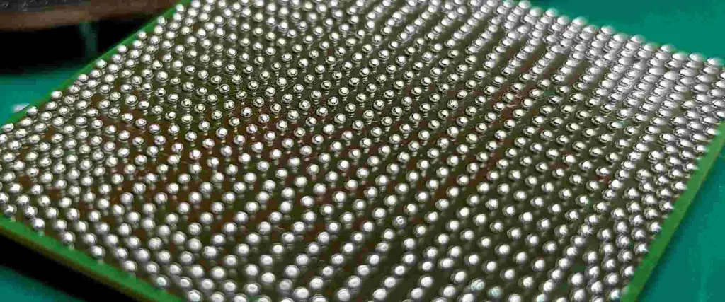
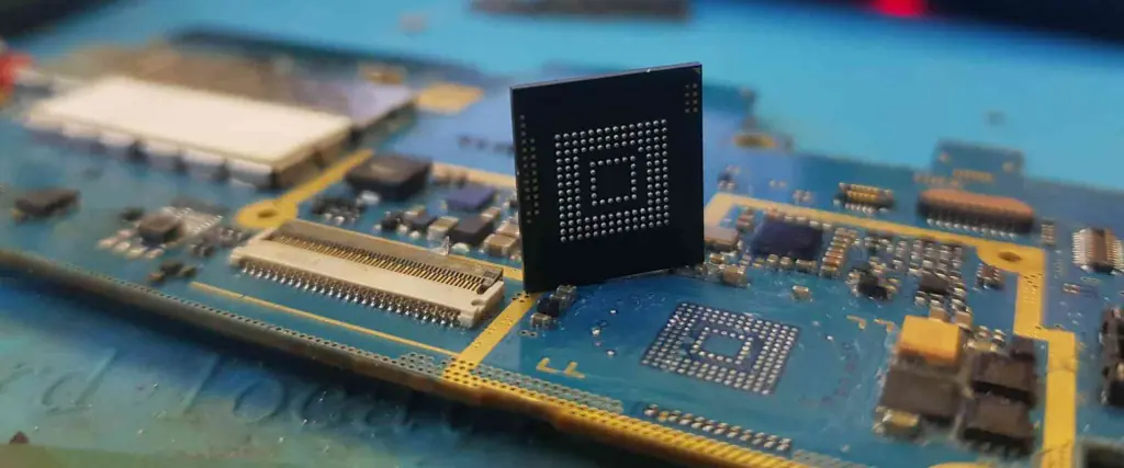
QFN (Quad Flat No-Lead) components are a type of surface-mount integrated circuit package. They are characterized by their flat profile, absence of leads, and exposed thermal pad on the bottom of the package. QFN components offer several advantages:

  • Smaller footprint
  • Improved thermal performance
  • Better electrical performance due to shorter connection paths
  • Lower parasitic inductance and capacitance

Common Applications of QFN Components

QFN components are widely used in various electronic applications, including:

  1. Mobile devices
  2. Automotive electronics
  3. Internet of Things (IoT) devices
  4. Consumer electronics
  5. Industrial control systems

Causes of Short Circuits to Ground in QFN Components

QFN
QFN

Understanding the root causes of short circuits is crucial for developing effective prevention strategies. Here are the main factors that can lead to short circuits in QFN components:
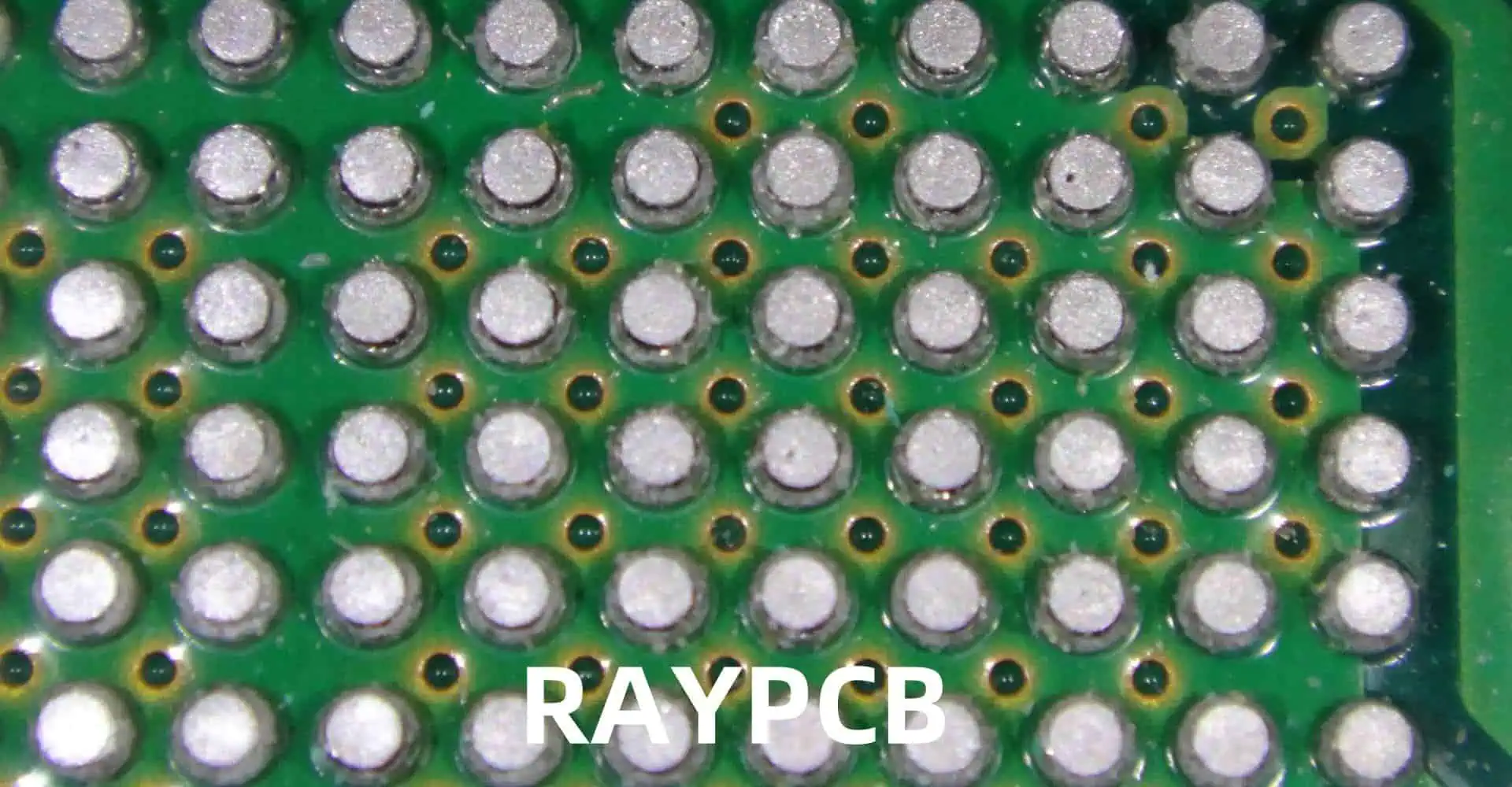
1. Solder Bridging

Solder bridging occurs when excess solder forms a conductive path between adjacent pads or between a pad and the exposed thermal pad. This is one of the most common causes of short circuits in QFN components.

2. Component Misalignment

Improper placement of the QFN component during assembly can result in pins contacting the wrong pads or the thermal pad, leading to short circuits.
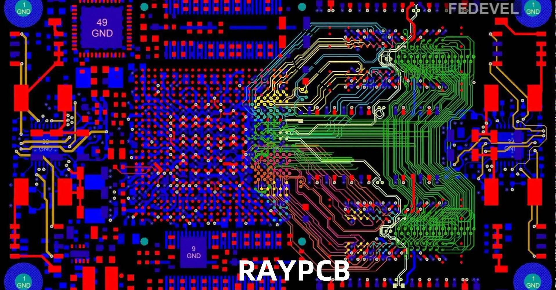
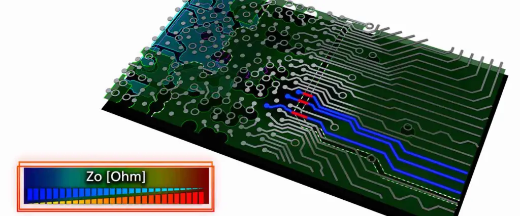
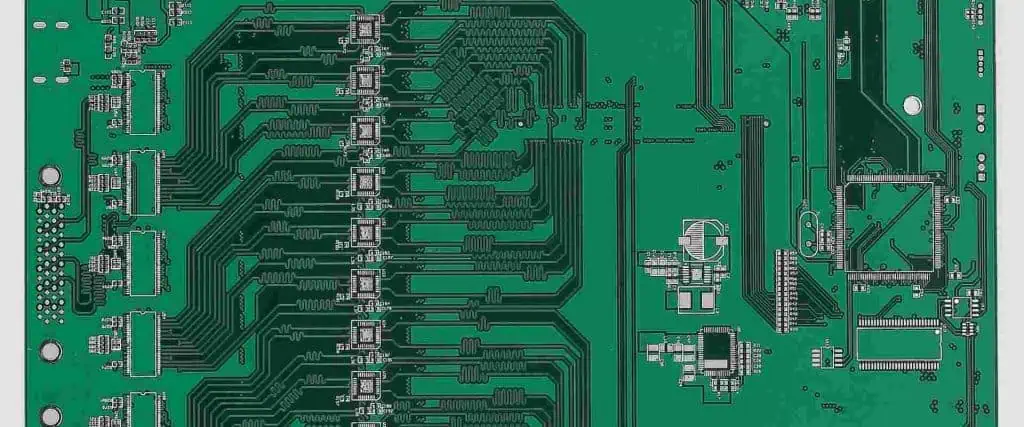
3. PCB Design Flaws

Inadequate spacing between pads, improper pad sizing, or incorrect thermal pad design can increase the risk of short circuits.

4. Contamination

Flux residues, moisture, or other contaminants can create conductive paths between pads and ground, causing intermittent or permanent short circuits.

5. Thermal Pad Issues

Overfilling or underfilling the thermal pad with solder can lead to component floating or solder balls, both of which can cause short circuits.

6. Mechanical Stress

Excessive mechanical stress during assembly or operation can cause component warpage or cracking, potentially leading to internal short circuits.

Preventing Short Circuits to Ground in QFN Components

To mitigate the risk of short circuits, a multi-faceted approach is necessary. Let’s explore various prevention strategies:

1. Optimizing PCB Design
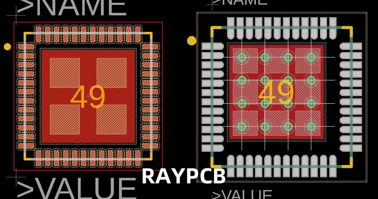
Proper Pad Design

  • Use the manufacturer’s recommended pad layout
  • Ensure adequate spacing between pads
  • Implement teardrop pads for improved solder flow

Thermal Pad Considerations

  • Design the thermal pad with proper segmentation
  • Use a grid of small vias for improved heat dissipation
  • Implement solder mask defined (SMD) pads for better control

Ground Plane Design

  • Use a solid ground plane beneath the QFN component
  • Implement ground plane cutouts to prevent solder bridging

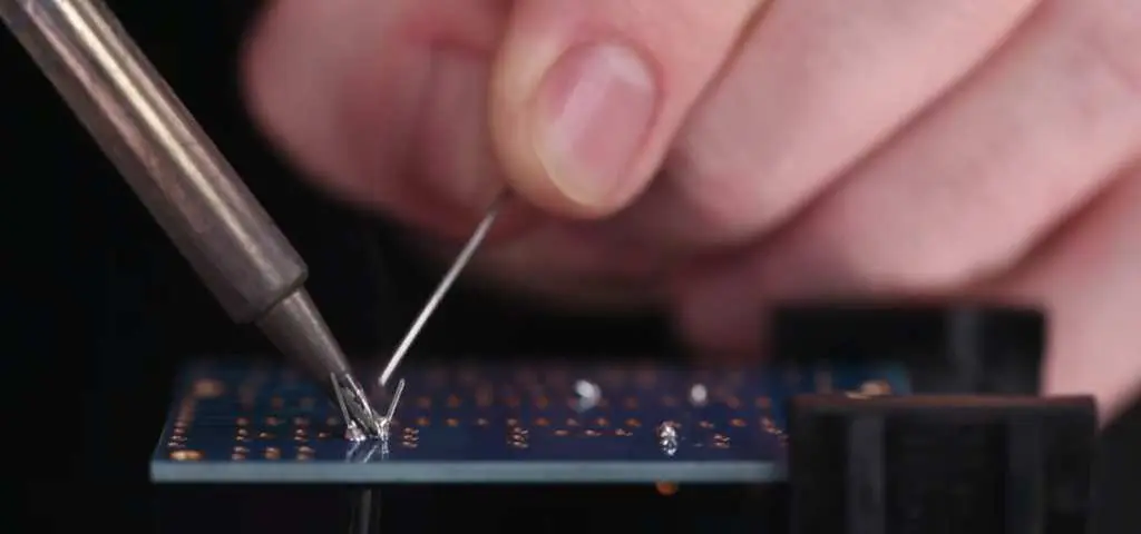
2. Improving Assembly Processes

Solder Paste Application

  • Use a high-quality, fine-pitch stencil
  • Optimize solder paste volume
  • Consider using Type 4 or Type 5 solder paste for finer pitch components

Component Placement

  • Use precision pick-and-place equipment
  • Implement optical alignment systems
  • Verify placement accuracy before reflow

Reflow Profile Optimization

  • Develop a reflow profile specific to QFN components
  • Monitor and control temperature ramp rates
  • Ensure proper peak temperature and time above liquidus

3. Implementing Inspection and Testing

Automated Optical Inspection (AOI)

  • Use high-resolution AOI systems
  • Develop custom algorithms for QFN inspection
  • Implement 3D AOI for improved defect detection

X-ray Inspection

  • Use X-ray systems to inspect hidden solder joints
  • Check for voids in the thermal pad solder
  • Verify internal component integrity

Electrical Testing

  • Perform in-circuit testing (ICT) for short circuit detection
  • Implement functional testing to verify proper operation
  • Use boundary scan testing for improved test coverage

4. Enhancing Cleaning and Contamination Control

Flux Selection

  • Use no-clean fluxes when possible
  • If cleaning is necessary, select easily removable fluxes

Cleaning Processes

  • Implement effective cleaning processes for flux removal
  • Use ultrasonic cleaning for hard-to-reach areas
  • Verify cleanliness using ionic contamination testing

Environmental Controls

  • Control humidity in storage and assembly areas
  • Implement proper handling procedures to prevent contamination
  • Use dry storage for moisture-sensitive components

5. Implementing Design for Manufacturability (DFM)

Component Selection

  • Choose QFN packages appropriate for your manufacturing capabilities
  • Consider using components with larger pitch for easier assembly

Fiducial Placement

  • Implement proper fiducial marks for accurate component placement
  • Use local fiducials for critical components

Testability Considerations

  • Design for testability to improve fault detection
  • Implement test points for critical nets

Best Practices for QFN Component Assembly

To summarize the key points for preventing short circuits in QFN components, here’s a table of best practices:

CategoryBest Practice
PCB Design– Use manufacturer-recommended pad layouts<br>- Implement proper thermal pad design<br>- Ensure adequate spacing between pads
Solder Paste Application– Use high-quality, fine-pitch stencils<br>- Optimize solder paste volume<br>- Consider using Type 4 or Type 5 solder paste
Component Placement– Use precision pick-and-place equipment<br>- Implement optical alignment systems<br>- Verify placement accuracy before reflow
Reflow Process– Develop QFN-specific reflow profiles<br>- Monitor and control temperature ramp rates<br>- Ensure proper peak temperature and time above liquidus
Inspection– Implement high-resolution AOI<br>- Use X-ray inspection for hidden solder joints<br>- Perform electrical testing for short circuit detection
Cleaning– Use no-clean fluxes when possible<br>- Implement effective cleaning processes<br>- Verify cleanliness using ionic contamination testing
Environmental Control– Control humidity in storage and assembly areas<br>- Implement proper handling

Advanced Techniques for Short Circuit Prevention

As technology advances, new techniques are being developed to further reduce the risk of short circuits in QFN components:

1. Conformal Coating

Applying a thin, protective layer of conformal coating can help prevent short circuits caused by contamination or moisture. However, care must be taken to ensure proper application and curing of the coating.

2. Underfill Technology

Using underfill materials can improve the mechanical stability of QFN components and prevent solder joint failures. This technique is particularly useful in applications subject to high vibration or thermal cycling.

3. Advanced PCB Materials

New PCB materials with improved thermal and electrical properties can help reduce the risk of short circuits. These materials often offer better dimensional stability and reduced moisture absorption.

4. Plasma Cleaning

Implementing plasma cleaning processes before and after assembly can significantly reduce contamination and improve solder joint reliability.

5. Machine Learning in Inspection

Incorporating machine learning algorithms into AOI and X-ray inspection systems can improve defect detection accuracy and reduce false positives.

Comparing Short Circuit Prevention Techniques

To help you choose the most appropriate techniques for your application, here’s a comparison table of various short circuit prevention methods:

Prevention TechniqueEffectivenessCostComplexityApplicability
Optimized PCB DesignHighLowModerateAll applications
Precision AssemblyHighModerateModerateAll applications
AOI and X-ray InspectionHighHighHighAll applications
Conformal CoatingModerateModerateLowMoisture-sensitive applications
Underfill TechnologyHighHighHighHigh-reliability applications
Advanced PCB MaterialsModerateHighLowHigh-performance applications
Plasma CleaningModerateModerateModerateAll applications
Machine Learning InspectionHighHighHighHigh-volume production

Conclusion

Preventing short circuits to ground in QFN components requires a comprehensive approach that addresses all aspects of the design and manufacturing process. By implementing the strategies outlined in this article, you can significantly reduce the risk of short circuits and improve the overall reliability of your electronic designs.

Remember that prevention is always more cost-effective than dealing with failures in the field. Invest time and resources in optimizing your design and manufacturing processes to ensure the long-term success of your products.

Frequently Asked Questions (FAQ)

Q1: How can I determine if a short circuit has occurred in a QFN component?

A1: Short circuits in QFN components can be detected through various methods:

  • Visual inspection using high-magnification microscopes or AOI systems
  • X-ray inspection to check for solder bridging or internal defects
  • Electrical testing, including in-circuit testing and functional testing
  • Thermal imaging to identify hot spots that may indicate a short circuit

Q2: Are there any specific design guidelines for the thermal pad of QFN components?

A2: Yes, some key guidelines for thermal pad design include:

  • Follow the manufacturer’s recommendations for pad size and layout
  • Use a grid of small vias for improved heat dissipation
  • Implement thermal pad segmentation to reduce the risk of solder bridging
  • Consider using solder mask defined (SMD) pads for better solder control

Q3: How does humidity affect the risk of short circuits in QFN components?

A3: High humidity can increase the risk of short circuits in QFN components by:

  • Promoting corrosion of exposed metal surfaces
  • Causing moisture absorption in PCB materials, leading to delamination
  • Facilitating the formation of conductive paths between pads due to moisture To mitigate these risks, control humidity in storage and assembly areas, and use moisture-resistant materials and coatings when appropriate.

Q4: What are the advantages of using X-ray inspection for QFN components?

A4: X-ray inspection offers several advantages for QFN components:

  • Ability to inspect hidden solder joints beneath the component
  • Detection of voids in the thermal pad solder
  • Verification of internal component integrity
  • Non-destructive inspection method
  • Capability to detect subtle defects that may not be visible with optical inspection

Q5: How can I optimize the reflow profile for QFN components?

A5: To optimize the reflow profile for QFN components:

  • Start with the component manufacturer’s recommended profile
  • Adjust the preheat slope to allow for proper flux activation and solvent evaporation
  • Ensure the peak temperature is sufficient to form reliable solder joints without damaging the component
  • Control the time above liquidus to allow proper wetting while preventing excessive intermetallic growth
  • Use thermocouples or thermal profiling equipment to verify and fine-tune the profile Remember to consider the thermal characteristics of other components on the PCB when developing the reflow profile.

Suppression Method of Signal Reflection in High-Speed PCB Layout

In the realm of high-speed printed circuit board (PCB) design, signal integrity is paramount. As clock speeds increase and edge rates become faster, the challenge of managing signal reflections becomes increasingly critical. Signal reflections can lead to distorted waveforms, false triggering, and reduced noise margins, ultimately compromising the reliability and performance of electronic systems. This article delves into the various methods and techniques for suppressing signal reflection in high-speed PCB layouts, providing designers with a comprehensive toolkit to ensure optimal signal integrity.

Understanding Signal Reflection

What Causes Signal Reflection?

Signal reflection occurs when an electrical signal encounters a discontinuity in the transmission line impedance. This discontinuity can be caused by various factors:

  1. Impedance mismatches
  2. Vias and layer transitions
  3. Connectors and component leads
  4. Trace width or layer changes
  5. Improper termination

The Impact of Reflections on Signal Integrity

Reflections can have several negative effects on signal integrity:

  1. Voltage overshoot and undershoot
  2. Ringing and oscillations
  3. Increased electromagnetic interference (EMI)
  4. Reduced timing margins
  5. False switching and logic errors

Impedance Matching Techniques

PCB Impedance

Controlled Impedance Traces

One of the fundamental techniques for reflection suppression is the use of controlled impedance traces.

Common Impedance Values

ApplicationTypical Impedance
Single-ended50ฮฉ or 75ฮฉ
Differential100ฮฉ or 120ฮฉ

Impedance Calculation

The impedance of a microstrip or stripline can be calculated using various formulas, considering factors such as trace width, dielectric thickness, and dielectric constant.

Stackup Considerations

Proper stackup design is crucial for maintaining consistent impedance throughout the board.

Stackup Best Practices

  1. Use adjacent ground planes for microstrip and stripline configurations
  2. Maintain consistent dielectric thickness
  3. Consider using high-speed laminates with stable dielectric constants

Termination Strategies

Series Termination

Series termination involves placing a resistor near the signal source to match the trace impedance.

Advantages of Series Termination

  1. Reduces reflections at the source
  2. Minimal impact on DC levels
  3. Low power consumption

Parallel Termination

Parallel termination uses a resistor at the end of the transmission line to match the characteristic impedance.

Types of Parallel Termination

  1. Simple parallel termination
  2. Thevenin termination
  3. AC termination

Active Termination

Active termination uses voltage-controlled current sources or other active components to dynamically match impedance.

Via Design and Optimization

Via Types and Selection

Choosing the appropriate via type is crucial for minimizing reflections at layer transitions.

Common Via Types

Via TypeDescriptionBest Use Case
Through-holeSpans all layersGeneral purpose
BlindConnects outer to inner layerHigh-density designs
BuriedConnects inner layersHigh-layer count boards
MicroviasSmall diameter, typically laser-drilledHDI designs

Via Stub Removal

Via stubs can cause significant reflections and should be minimized or eliminated.

Stub Reduction Techniques

  1. Back-drilling
  2. Buried vias
  3. Stacked microvias

Via Spacing and Placement

Proper via spacing and placement can help maintain signal integrity.

Via Placement Guidelines

  1. Place vias close to the source for series-terminated lines
  2. Use multiple vias for power and ground connections
  3. Maintain consistent via spacing for differential pairs

Trace Routing Techniques

Length Matching

Matching trace lengths is crucial for maintaining timing relationships and reducing reflections in parallel buses.

Length Matching Tolerance

Signal TypeTypical Tolerance
Single-endedยฑ5% of total length
Differentialยฑ2.5% of total length

Serpentine Routing

Serpentine routing is used to add length to shorter traces for length matching purposes.

Serpentine Design Rules

  1. Maintain minimum bend radius
  2. Avoid sharp corners (use 45-degree or arc bends)
  3. Keep serpentines away from sensitive areas

Differential Pair Routing

Proper differential pair routing is essential for maintaining common-mode rejection and reducing reflections.

Differential Routing Guidelines

  1. Maintain consistent spacing between the pair
  2. Route differential pairs closely coupled
  3. Avoid splits in the reference plane beneath the pair

Power Integrity and Its Impact on Reflections

Proper Decoupling

Effective decoupling reduces power supply noise and helps maintain signal integrity.

Decoupling Capacitor Selection

Frequency RangeCapacitor Type
Low (< 10 MHz)Bulk electrolytic
Medium (10 MHz – 100 MHz)Ceramic MLCC
High (> 100 MHz)Low-ESR ceramic

Power Plane Design

Well-designed power planes provide low-impedance power distribution and help reduce reflections.

Power Plane Best Practices

  1. Use solid planes rather than traces for power distribution
  2. Implement proper plane separation
  3. Use stitching vias to connect split planes

Advanced Reflection Suppression Techniques

Pre-emphasis and De-emphasis

Pre-emphasis and de-emphasis techniques can be used to compensate for channel losses and reduce reflections.

Pre-emphasis Implementation

  1. Transmitter-based pre-emphasis
  2. Receiver-based equalization
  3. Adaptive equalization techniques

Spread Spectrum Clocking

Spread spectrum clocking can help reduce EMI and mitigate the effects of reflections.

Spread Spectrum Parameters

ParameterTypical Range
Modulation Rate30-33 kHz
Modulation Amplitude0.5-1% of center frequency

Electromagnetic Band Gap (EBG) Structures

EBG structures can be used to suppress specific frequency bands and reduce reflections.

EBG Applications

  1. Power plane noise suppression
  2. Isolation of sensitive circuits
  3. Reduction of edge-launched surface waves

Signal Integrity Simulation and Analysis

Time Domain Reflectometry (TDR)

TDR analysis is a powerful tool for identifying and locating impedance discontinuities.

TDR Measurement Parameters

  1. Rise time
  2. Incident voltage
  3. Reflection coefficient

S-Parameter Analysis

S-parameters provide a comprehensive characterization of high-speed interconnects.

Key S-Parameters

  1. S11 (Return Loss)
  2. S21 (Insertion Loss)
  3. S31 (Near-end Crosstalk)
  4. S41 (Far-end Crosstalk)

Eye Diagram Analysis

Eye diagrams offer a visual representation of signal quality and can help identify reflection-related issues.

Eye Diagram Metrics

  1. Eye height
  2. Eye width
  3. Jitter
  4. Bit error rate (BER)

PCB Material Considerations

Dielectric Material Selection

Choosing the right dielectric material is crucial for maintaining consistent impedance and reducing signal loss.

Common High-Speed PCB Materials

MaterialDk RangeDf RangeBest Use Case
FR-43.8-4.80.01-0.02General purpose
Rogers 4350B3.480.0037High-frequency
Megtron 63.40.002Low-loss, high-speed

Copper Foil Considerations

The type and quality of copper foil can impact signal integrity and reflection suppression.

Copper Foil Types

  1. Standard ED copper
  2. Reverse-treated foil (RTF)
  3. Very low profile (VLP) foil

Manufacturing and Testing Considerations

Controlled Impedance Manufacturing

Working closely with PCB manufacturers to ensure controlled impedance fabrication is crucial.

Manufacturing Specifications

  1. Dielectric thickness tolerances
  2. Copper thickness tolerances
  3. Trace width tolerances

Signal Integrity Testing

Implementing comprehensive signal integrity testing helps verify reflection suppression efforts.

Testing Methods

  1. Vector Network Analyzer (VNA) measurements
  2. TDR/TDT testing
  3. Bit Error Rate Testing (BERT)

Conclusion

Suppressing signal reflections in high-speed PCB layouts requires a multifaceted approach, combining proper design techniques, material selection, and advanced analysis methods. By implementing the strategies outlined in this article, PCB designers can significantly improve signal integrity, leading to more reliable and higher-performing electronic systems.

Frequently Asked Questions

Q1: How do I determine if signal reflection is a significant issue in my PCB design?

A1: Several indicators can suggest that signal reflection is a significant issue:

  1. Ringing or oscillations on signal waveforms
  2. Unexplained EMI problems
  3. Intermittent system failures or data errors
  4. Poor eye diagram measurements (reduced eye height or width)
  5. Failed signal integrity tests (e.g., TDR measurements showing large discontinuities)

To determine if reflection is the root cause, you can:

  • Perform time-domain reflectometry (TDR) analysis
  • Conduct S-parameter measurements
  • Use signal integrity simulation tools to model and analyze the design
  • Examine eye diagrams for signal quality issues

If these analyses reveal significant impedance discontinuities or waveform distortions, signal reflection is likely a concern that needs to be addressed.

Q2: What are the trade-offs between different termination methods?

A2: The main termination methods (series, parallel, and active) each have their own trade-offs:

  1. Series Termination:
    • Pros: Low power consumption, minimal impact on DC levels
    • Cons: Signal delay, not suitable for multi-drop buses
  2. Parallel Termination:
    • Pros: Effective for multi-drop buses, maintains signal integrity at receiver
    • Cons: Higher power consumption, can impact DC levels
  3. Active Termination:
    • Pros: Adaptable to changing conditions, can handle complex impedance matching
    • Cons: Higher cost, increased complexity, potential for additional noise

The choice depends on factors such as:

  • Signal characteristics (frequency, rise time)
  • Board topology (point-to-point vs. multi-drop)
  • Power budget
  • Cost constraints
  • Available board space

Consider these factors carefully when selecting the most appropriate termination method for your specific design requirements.

Q3: How can I effectively manage reflections in high-speed differential pairs?

A3: Managing reflections in high-speed differential pairs involves several key strategies:

  1. Maintain consistent differential impedance (typically 100ฮฉ or 120ฮฉ) throughout the entire path.
  2. Use symmetrical routing to ensure equal length and impedance for both signals in the pair.
  3. Keep the pair tightly coupled to maintain common-mode rejection.
  4. Avoid splits in the reference plane beneath the differential pair.
  5. Use appropriate differential termination techniques, such as:
    • Differential series termination near the source
    • Differential parallel termination at the receiver
  6. Minimize via transitions and ensure symmetry when transitions are necessary.
  7. Use matched-length vias for layer changes.
  8. Implement careful length matching between pairs in multi-pair buses.
  9. Consider using high-quality, low-loss PCB materials for critical differential pairs.
  10. Perform differential TDR and eye diagram analysis to verify pair performance.

By applying these techniques, you can significantly reduce reflections and maintain signal integrity in high-speed differential pairs.

Q4: What role does PCB stackup design play in reflection suppression?

A4: PCB stackup design plays a crucial role in reflection suppression:

  1. Impedance Control: Proper stackup ensures consistent impedance for signal layers, minimizing reflections due to impedance variations.
  2. Return Path: A well-designed stackup provides continuous return paths for high-speed signals, reducing discontinuities.
  3. Crosstalk Reduction: Strategic layer ordering and spacing can minimize crosstalk, which can contribute to reflections.
  4. Power Integrity: Incorporating dedicated power and ground planes helps maintain a stable power distribution network, reducing noise-induced reflections.
  5. Via Performance: The stackup influences via stub length and overall via performance, affecting signal transitions between layers.
  6. Dielectric Thickness: Consistent dielectric thickness between layers helps maintain uniform impedance.
  7. Material Selection: The stackup determines which materials are used for each layer, impacting overall signal loss and impedance stability.
  8. EMI Control: Proper shielding layers in the stackup can reduce EMI, which can indirectly contribute to signal integrity issues.

A carefully designed stackup is foundational to effective reflection suppression in high-speed PCB layouts.

Q5: How do I balance reflection suppression techniques with other design constraints like cost and manufacturability?

A5: Balancing reflection suppression with cost and manufacturability involves several considerations:

  1. Material Selection:
    • Use standard FR-4 for less critical signals
    • Reserve high-performance (and costlier) materials for critical high-speed sections
  2. Layer Count:
    • Optimize layer count to balance signal integrity needs with cost
    • Consider using hybrid stackups with selective use of high-performance materials
  3. Via Strategy:
    • Use through-hole vias where possible for lower cost
    • Implement back-drilling or blind/buried vias only for critical signals
  4. Termination:
    • Use series termination where applicable to reduce component count
    • Implement parallel termination judiciously, considering power consumption
  5. Trace Geometry:
    • Design traces within standard manufacturing tolerances
    • Use controlled impedance only where necessary
  6. Component Selection:
    • Choose components with integrated termination or ESD protection to reduce BOM complexity
  7. Design for Testability:
    • Incorporate test points for critical signals to enable easier manufacturing verification
  8. Simulation and Analysis:
    • Utilize simulation tools early in the design process to optimize designs before committing to manufacturing
  9. Manufacturing Partnerships:
    • Work closely with PCB manufacturers to understand their capabilities and limitations
  10. Design Rules:
    • Develop and adhere to design rules that balance performance requirements with manufacturability

By carefully considering these factors, you can achieve effective reflection suppression while maintaining reasonable cost and manufacturability in your high-speed PCB designs.

Visual Inspection: A Shortcut to Cost Reduction and Reliability Improvement of Electronics Manufacturing

In the competitive landscape of electronics manufacturing, companies are constantly seeking ways to reduce costs while maintaining or improving product reliability. Visual inspection, often overlooked in favor of more advanced automated testing methods, remains a crucial shortcut to achieving both cost reduction and reliability improvement. This article explores the significance of visual inspection in electronics manufacturing, its implementation strategies, and the tangible benefits it brings to the production process.

The Importance of Visual Inspection in Electronics Manufacturing

Definition and Scope

Visual inspection in electronics manufacturing refers to the process of examining components, printed circuit boards (PCBs), assemblies, and finished products using the human eye, often aided by magnification tools. It encompasses various stages of production, from incoming component inspection to final product evaluation.

Role in Quality Assurance

Visual inspection serves as a critical first line of defense in quality assurance, capable of detecting a wide range of defects that may be missed by automated testing systems.

Types of Defects Detectable by Visual Inspection

Visual Inspection PCBA
Defect CategoryExamples
Component DefectsMisalignment, wrong polarity, missing components
Soldering IssuesInsufficient solder, solder bridges, cold joints
PCB DefectsScratches, delamination, copper exposure
Assembly ProblemsBent pins, lifted leads, foreign material
Cosmetic IssuesDiscoloration, surface damage, label errors

Implementing Effective Visual Inspection Processes

Training and Qualification of Inspectors

Developing a skilled workforce of visual inspectors is crucial for the success of the inspection process.

Key Elements of Inspector Training

  1. Understanding of product specifications and quality standards
  2. Familiarity with common defect types and their visual characteristics
  3. Proper use of inspection tools and equipment
  4. Ergonomics and eye strain prevention techniques
  5. Documentation and reporting procedures

Inspection Environment and Tools

Creating an optimal inspection environment enhances the accuracy and efficiency of visual inspections.

Essential Elements of an Inspection Workstation

ElementPurpose
LightingProper illumination to reveal defects
MagnificationDetailed examination of small components
Ergonomic SeatingComfort for extended inspection periods
Anti-static EquipmentPrevention of ESD damage
Documentation AccessQuick reference to specifications

Inspection Criteria and Checklists

Developing clear, standardized inspection criteria ensures consistency across inspectors and shifts.

Sample Visual Inspection Checklist

  1. Component presence and orientation
  2. Solder joint quality and uniformity
  3. PCB surface condition
  4. Dimensional accuracy of assemblies
  5. Labeling and marking accuracy
  6. Cleanliness and absence of foreign materials

Integration with Production Workflow

Seamless integration of visual inspection into the production process maximizes its effectiveness without compromising efficiency.

Strategic Inspection Points

  1. Incoming component inspection
  2. Post-placement inspection (before reflow)
  3. Post-reflow inspection
  4. Final assembly inspection
  5. Pre-packaging inspection

Cost Reduction Through Visual Inspection

9 PCB inspection precautions

Early Defect Detection

Identifying defects early in the production process significantly reduces the cost of rework and scrap.

Cost Savings Example

Stage of DetectionRelative Cost to Correct
Component Level1x
PCB Assembly10x
Final Product100x
Field Failure1000x

Reduction in Automated Testing Time

Effective visual inspection can reduce the reliance on time-consuming automated testing procedures.

Minimization of Customer Returns

Catching cosmetic and functional defects before shipment reduces costly customer returns and warranty claims.

Process Improvement Insights

Visual inspection provides valuable feedback for continuous improvement of manufacturing processes.

Reliability Improvement Through Visual Inspection

Prevention of Latent Defects

Many reliability issues stem from defects that are not immediately apparent but can be detected through careful visual inspection.

Examples of Latent Defects Detectable by Visual Inspection

  1. Insufficient solder on critical connections
  2. Microscopic cracks in PCB traces
  3. Improper component placement leading to stress
  4. Contamination that could cause long-term corrosion

Enhanced Process Control

Regular visual inspections help maintain tight control over manufacturing processes, ensuring consistent quality.

Identification of Systemic Issues

Patterns observed during visual inspection can reveal systemic problems in design or production processes.

Compliance with Industry Standards

Visual inspection plays a crucial role in meeting industry standards and regulatory requirements.

Relevant Industry Standards

StandardFocus Area
IPC-A-610Acceptability of Electronic Assemblies
J-STD-001Requirements for Soldered Electrical and Electronic Assemblies
MIL-STD-883Test Method Standard for Microcircuits

Advanced Visual Inspection Techniques

Automated Optical Inspection (AOI)

While not strictly “visual” in the traditional sense, AOI systems complement manual inspection processes.

Benefits of AOI Integration

  1. High-speed inspection of large production volumes
  2. Consistent application of inspection criteria
  3. Digital documentation of inspection results
  4. Ability to detect defects beyond human visual acuity

Machine Learning in Visual Inspection

Emerging AI technologies are enhancing the capabilities of both manual and automated visual inspection processes.

Applications of Machine Learning in Visual Inspection

  1. Defect classification and categorization
  2. Predictive maintenance of inspection equipment
  3. Optimization of inspection parameters
  4. Anomaly detection in complex assemblies

3D Inspection Technologies

Advanced 3D inspection systems provide additional dimensions of analysis for complex assemblies.

Types of 3D Inspection Technologies

  1. Laser triangulation
  2. Structured light scanning
  3. Computed tomography (CT) scanning

Challenges and Limitations of Visual Inspection

Human Factors

Visual inspection is subject to human limitations and variability.

Common Human Factor Challenges

  1. Fatigue and attention span
  2. Subjective interpretation of defects
  3. Inconsistency between inspectors
  4. Eye strain and ergonomic issues

Scalability Concerns

As production volumes increase, maintaining thorough visual inspection becomes challenging.

Invisible Defects

Some defects may not be visible even with magnification, requiring additional testing methods.

Best Practices for Implementing Visual Inspection

bga inspection

Standardization and Documentation

Develop and maintain detailed inspection standards and procedures.

Continuous Training and Certification

Implement ongoing training programs to maintain and improve inspector skills.

Regular Audits and Calibration

Conduct periodic audits of the inspection process and calibrate inspection equipment regularly.

Integration of Multiple Inspection Methods

Combine visual inspection with other testing methods for comprehensive quality assurance.

Feedback Loop Implementation

Establish a system for inspectors to provide feedback on recurring issues or process improvements.

Future Trends in Visual Inspection for Electronics Manufacturing

Augmented Reality (AR) in Inspection

AR technologies promise to enhance inspector capabilities by overlaying digital information onto physical products.

Collaborative Robotics

Cobots may assist human inspectors in handling and manipulating products during inspection.

Big Data Analytics

Leveraging big data from inspection processes can provide insights for predictive quality management.

Conclusion

Visual inspection remains a powerful tool in the arsenal of electronics manufacturers seeking to reduce costs and improve reliability. By implementing robust visual inspection processes, companies can catch defects early, streamline production, and ensure the delivery of high-quality products to their customers. As technology advances, the integration of visual inspection with automated systems and AI promises to further enhance its effectiveness, cementing its role as a critical component of modern electronics manufacturing.

Frequently Asked Questions

Q1: How does visual inspection compare to automated testing methods in terms of cost-effectiveness?

A1: Visual inspection is often more cost-effective than automated testing methods for several reasons:

  1. Lower initial investment: Visual inspection requires minimal equipment compared to complex automated systems.
  2. Flexibility: Inspectors can quickly adapt to new products or quality criteria without reprogramming.
  3. Early defect detection: Visual inspection can catch issues earlier in the production process, reducing costly rework.
  4. Comprehensive defect detection: Human inspectors can often spot unusual or unexpected defects that automated systems might miss.

However, for high-volume production, a combination of visual and automated inspection often provides the best balance of cost-effectiveness and thoroughness.

Q2: What are the key factors in training effective visual inspectors?

A2: Training effective visual inspectors involves several key factors:

  1. Product knowledge: Thorough understanding of the products and their specifications.
  2. Defect recognition: Ability to identify and classify various types of defects.
  3. Attention to detail: Developing keen observational skills and focus.
  4. Consistency: Training in applying standards uniformly across different products and situations.
  5. Tool proficiency: Proper use of magnification and other inspection tools.
  6. Ergonomics: Techniques to maintain focus and prevent fatigue during long inspection sessions.
  7. Documentation: Skills in accurately recording and reporting inspection results.
  8. Continuous learning: Ongoing training to keep up with new technologies and standards.

Q3: How can companies measure the ROI of implementing or improving visual inspection processes?

A3: Companies can measure the ROI of visual inspection improvements through several metrics:

  1. Defect escape rate: Reduction in defects caught by customers or later testing stages.
  2. Rework costs: Decrease in expenses related to fixing defects later in production.
  3. Customer returns: Reduction in product returns due to quality issues.
  4. Production yield: Increase in first-pass yield rates.
  5. Inspection time: Efficiency improvements in the inspection process itself.
  6. Warranty claims: Reduction in long-term reliability issues caught by customers.
  7. Customer satisfaction: Improvements in customer feedback and ratings.

By tracking these metrics before and after implementing visual inspection improvements, companies can quantify the financial benefits and calculate ROI.

Q4: What are the limitations of visual inspection, and how can they be mitigated?

A4: Visual inspection has several limitations:

  1. Subjectivity: Different inspectors may interpret defects differently.
  2. Fatigue: Long inspection sessions can lead to decreased accuracy.
  3. Speed: Manual inspection can be slower than automated methods for high volumes.
  4. Invisible defects: Some issues may not be detectable by eye.

These limitations can be mitigated by:

  1. Implementing standardized inspection criteria and regular calibration exercises.
  2. Rotating inspectors and providing ergonomic workstations to reduce fatigue.
  3. Using a hybrid approach combining visual and automated inspection methods.
  4. Supplementing visual inspection with other testing techniques (e.g., X-ray, in-circuit testing) for comprehensive quality assurance.

Q5: How is artificial intelligence (AI) changing the landscape of visual inspection in electronics manufacturing?

A5: AI is transforming visual inspection in several ways:

  1. Automated defect detection: AI algorithms can analyze images to identify defects with high accuracy and speed.
  2. Consistency: AI systems apply consistent criteria across large volumes of products.
  3. Learning and adaptation: Machine learning models can improve over time, learning to detect new types of defects.
  4. Data analysis: AI can process vast amounts of inspection data to identify trends and predict quality issues.
  5. Augmented human inspection: AI can assist human inspectors by highlighting potential defects or providing decision support.
  6. Integration with other systems: AI can combine visual data with other sensor inputs for more comprehensive quality assessment.

While AI is enhancing visual inspection capabilities, it’s important to note that human expertise remains valuable, especially for complex or novel defect types. The future of visual inspection likely lies in the effective collaboration between human inspectors and AI systems.

Ultiboard PCB Design Tutorial

Ultiboard is a powerful printed circuit board (PCB) design software developed by National Instruments. It offers a comprehensive suite of tools for creating professional-grade PCB layouts. This tutorial will guide you through the process of designing a PCB using Ultiboard, from initial setup to final production files.

Getting Started with Ultiboard

System Requirements

Before installing Ultiboard, ensure your system meets the following requirements:

ComponentMinimum Requirement
Operating SystemWindows 10 (64-bit)
ProcessorIntel Core i5 or equivalent
RAM8 GB
Hard Disk Space5 GB free space
GraphicsDirectX 11 compatible

Installation Process

  1. Download the Ultiboard installer from the National Instruments website
  2. Run the installer and follow the on-screen instructions
  3. Activate your license or choose the trial version

Ultiboard Interface Overview

Familiarize yourself with the main components of the Ultiboard interface:

  1. Design Toolbox
  2. Component Bin
  3. Design Rules Manager
  4. Layer Manager
  5. Properties Window
  6. Design Canvas

Setting Up a New PCB Project

Creating a New Project

  1. Launch Ultiboard
  2. Click on “File” > “New” > “PCB Design”
  3. Choose a template or start with a blank design

Configuring Board Settings

  1. Set the board size and shape
  2. Define the number of layers
  3. Specify the grid settings

Importing Schematic

  1. If using Multisim, go to “Transfer” > “Transfer to Ultiboard”
  2. For other formats, use “File” > “Import” and select the appropriate file type

Component Placement

Understanding Component Types

Ultiboard supports various component types:

  1. Through-hole components
  2. Surface-mount devices (SMD)
  3. Connectors
  4. Custom components

Placing Components

  1. Select components from the Component Bin
  2. Click on the design canvas to place components
  3. Use the Properties Window to adjust component attributes

Component Arrangement Techniques

  1. Logical grouping of related components
  2. Consideration of signal flow
  3. Thermal management concerns

Routing Techniques

Manual Routing

  1. Select the “Route Manual” tool
  2. Click on component pins to start routing
  3. Use the Properties Window to adjust trace width and layer

Auto-routing

  1. Configure auto-router settings
  2. Select nets to auto-route
  3. Run the auto-router

Differential Pair Routing

  1. Identify differential pairs in your design
  2. Use the “Differential Pair” routing tool
  3. Maintain consistent trace length and spacing

Design Rule Checking (DRC)

Setting Up Design Rules

  1. Open the Design Rules Manager
  2. Define clearance rules
  3. Set trace width and via size rules
  4. Establish manufacturing constraints

Running DRC

  1. Go to “Tools” > “Design Rule Check”
  2. Select rule sets to check
  3. Review and address any violations

Power and Ground Planes

Creating Power Planes

  1. Add a new layer for the power plane
  2. Use the “Copper Pour” tool to create the plane
  3. Connect components to the plane using thermal reliefs

Designing Ground Planes

  1. Dedicate a layer for the ground plane
  2. Use a solid copper pour for optimal performance
  3. Ensure proper connection of components to the ground plane

Advanced Techniques

High-Speed Design Considerations

  1. Controlled impedance routing
  2. Signal integrity analysis
  3. EMI/EMC considerations

Flex and Rigid-Flex PCB Design

  1. Defining flex regions
  2. Placement of components on flex areas
  3. Special routing considerations for flex circuits

3D Visualization and Checking

  1. Enable 3D view mode
  2. Check for component clearances and interference
  3. Verify board fit within enclosures

Manufacturing Output

Generating Gerber Files

  1. Go to “File” > “Export” > “Gerber/Excellon Files”
  2. Configure layer mapping
  3. Set aperture and drill sizes

Creating Bill of Materials (BOM)

  1. Use “Tools” > “Reports” > “Bill of Materials”
  2. Customize BOM format and content
  3. Export to desired file format (e.g., CSV, Excel)

Design for Manufacturing (DFM) Checks

  1. Run final DRC with manufacturing rules
  2. Check for silkscreen overlaps
  3. Verify drill and via sizes

Tips for Efficient PCB Design in Ultiboard

Keyboard Shortcuts

ActionShortcut
Zoom InCtrl + +
Zoom OutCtrl + –
PanSpacebar + Left Mouse Button
Rotate ComponentR
Switch LayersShift + Up/Down Arrow

Using Custom Libraries

  1. Create custom component libraries for frequently used parts
  2. Import third-party libraries for expanded component selection

Design Versioning

  1. Use meaningful file naming conventions
  2. Implement a version control system for your PCB designs

Troubleshooting Common Issues

Dealing with Unrouted Nets

  1. Verify component connections in the schematic
  2. Check for disconnected pins or floating nets
  3. Use the “Highlight Net” feature to trace problematic connections

Resolving DRC Violations

  1. Systematically address each violation category
  2. Use the “Violation Browser” to navigate through issues
  3. Consider adjusting design rules if necessary

Optimizing Auto-router Performance

  1. Place critical components manually before auto-routing
  2. Define routing keepouts for sensitive areas
  3. Experiment with different auto-router strategies

Frequently Asked Questions

Q1: How does Ultiboard compare to other PCB design software?

A1: Ultiboard offers several advantages:

  1. Seamless integration with Multisim for schematic capture
  2. User-friendly interface suitable for beginners and professionals
  3. Powerful auto-routing capabilities
  4. Comprehensive design rule checking
  5. 3D visualization features

However, it may have a steeper learning curve compared to some entry-level PCB design tools and might lack some advanced features found in high-end professional software.

Q2: Can I import designs from other PCB software into Ultiboard?

A2: Yes, Ultiboard supports importing designs from various formats:

  1. ODB++ format for PCB layouts
  2. IPC-2581 format for board designs
  3. Gerber files for individual layers
  4. DXF files for mechanical layers

To import, use the “File” > “Import” menu and select the appropriate file type. However, note that some design elements may not translate perfectly between different software platforms, so always review imported designs carefully.

Q3: How can I ensure my Ultiboard design is ready for manufacturing?

A3: To prepare your Ultiboard design for manufacturing:

  1. Run a comprehensive Design Rule Check (DRC) with manufacturing-specific rules
  2. Generate and verify Gerber files for all necessary layers
  3. Create an accurate Bill of Materials (BOM)
  4. Produce assembly drawings with component placement information
  5. Conduct a final visual inspection in 3D view mode
  6. Consider sending your design to your PCB manufacturer for a DFM (Design for Manufacturing) review

Q4: What are some best practices for organizing complex designs in Ultiboard?

A4: For complex designs in Ultiboard, consider the following practices:

  1. Use a hierarchical approach with multiple sheets for large schematics
  2. Implement a consistent naming convention for nets, components, and layers
  3. Utilize custom libraries for frequently used components
  4. Create separate routing layers for different signal types (e.g., digital, analog, power)
  5. Use design partitioning for very large boards or modular designs
  6. Maintain detailed documentation of design decisions and revisions

Q5: How can I optimize the auto-routing process in Ultiboard for better results?

A5: To optimize auto-routing in Ultiboard:

  1. Manually place and route critical components and nets before auto-routing
  2. Set up appropriate design rules and constraints before running the auto-router
  3. Use routing keepouts to protect sensitive areas of the board
  4. Experiment with different auto-routing strategies and settings
  5. Consider using a combination of auto-routing and manual touch-up for best results
  6. Break down the auto-routing process into stages, focusing on different net classes or board areas in each stage

Remember that while auto-routing can be a useful tool, critical or high-speed sections of your design may still require manual routing for optimal performance.

A Comprehensive Introduction of IoT Based on RFID

The Internet of Things (IoT) has revolutionized the way we interact with our environment, connecting physical objects to the digital world. Among the various technologies enabling IoT, Radio Frequency Identification (RFID) plays a crucial role in bridging the gap between the physical and digital realms. This comprehensive introduction explores the intersection of IoT and RFID, delving into their synergies, applications, and the transformative potential they offer across various industries.

Understanding IoT and RFID

What is IoT?

The Internet of Things refers to the network of interconnected physical devices, vehicles, home appliances, and other items embedded with electronics, software, sensors, and network connectivity, which enables these objects to collect and exchange data.

What is RFID?

Radio Frequency Identification is a technology that uses electromagnetic fields to automatically identify and track tags attached to objects. RFID systems consist of three main components:

  1. RFID tags (or transponders)
  2. RFID readers (or interrogators)
  3. RFID middleware

Key Components of RFID Systems

ComponentFunction
RFID TagStores and transmits data about the object it’s attached to
RFID ReaderSends radio waves to read data from tags
AntennaEnables communication between tags and readers
MiddlewareProcesses and manages data from RFID readers

The Role of RFID in IoT

Enabling Object Identification

RFID serves as a foundational technology for IoT by providing a means to uniquely identify physical objects in the digital realm.

Data Collection and Transmission

RFID tags can store and transmit data about objects, including:

  1. Identification numbers
  2. Product details
  3. Location information
  4. Environmental conditions (with sensor-enabled tags)

Real-time Tracking and Monitoring

RFID enables real-time tracking of objects, facilitating:

  1. Supply chain visibility
  2. Asset management
  3. Inventory control
  4. Process optimization

RFID Technologies in IoT

Types of RFID Systems

Passive RFID

  • No internal power source
  • Powered by electromagnetic energy from the reader
  • Shorter read range (up to 10 meters)
  • Lower cost and longer lifespan

Active RFID

  • Internal power source (battery)
  • Longer read range (up to 100 meters or more)
  • Higher data transmission capabilities
  • More expensive but suitable for real-time locating systems (RTLS)

Semi-passive RFID

  • Battery-assisted passive tags
  • Longer read range than passive tags
  • Used in specific applications requiring enhanced performance

RFID Frequency Bands

Frequency BandCharacteristicsTypical Applications
Low Frequency (LF)Short range, penetrates water and metalAnimal tracking, access control
High Frequency (HF)Medium range, good for liquids and metalsPayment systems, smart cards
Ultra-High Frequency (UHF)Long range, fast data transferSupply chain, inventory management
MicrowaveLongest range, highest data rateVehicle tracking, electronic toll collec

Integration of RFID with IoT Platforms

RFID Data Processing

  1. Data capture from RFID readers
  2. Filtering and aggregation of raw data
  3. Event processing and pattern recognition

Middleware and Cloud Integration

  1. RFID middleware for data management
  2. Integration with enterprise systems (ERP, WMS, etc.)
  3. Cloud-based data storage and analytics

Edge Computing in RFID-IoT Systems

  1. Processing data closer to the source
  2. Reducing latency and bandwidth usage
  3. Enabling real-time decision making

Applications of RFID in IoT Ecosystems

intel iot
intel iot

Supply Chain and Logistics

Inventory Management

  • Real-time visibility of stock levels
  • Automated reordering systems
  • Reduction of stockouts and overstock situations

Asset Tracking

  • Tracking of containers, pallets, and high-value assets
  • Improved asset utilization and reduced loss

Cold Chain Monitoring

  • Temperature monitoring for perishable goods
  • Ensuring product quality and compliance

Retail and Consumer Goods

Smart Shelves

  • Automated inventory tracking
  • Dynamic pricing based on demand and expiration dates

Anti-counterfeiting

  • Authentication of luxury goods and pharmaceuticals
  • Tracking product lifecycle from manufacture to sale

Interactive Customer Experiences

  • Product information retrieval via smartphone apps
  • Personalized recommendations based on shopping history

Healthcare and Pharmaceuticals

Patient Tracking

  • Real-time location of patients in hospitals
  • Improved workflow and patient safety

Medication Management

  • Tracking of medication from pharmacy to patient
  • Ensuring correct dosage and preventing errors

Equipment Tracking

  • Locating and managing medical equipment
  • Optimizing equipment utilization and maintenance

Manufacturing and Industrial IoT

Production Line Optimization

  • Real-time tracking of work-in-progress
  • Quality control and defect tracking

Maintenance and Repair

  • Predictive maintenance based on usage data
  • Streamlined repair processes with accurate part identification

Safety and Compliance

  • Tracking of personal protective equipment (PPE)
  • Ensuring compliance with safety regulations

Smart Cities and Infrastructure

Waste Management

  • Optimizing waste collection routes
  • Pay-as-you-throw systems for residential waste

Public Transportation

  • Contactless ticketing systems
  • Real-time vehicle tracking and passenger information

Access Control and Security

  • RFID-enabled access cards for buildings and areas
  • Integration with smart city security systems

Challenges and Considerations

Security and Privacy

  1. Encryption of RFID data
  2. Authentication mechanisms for RFID systems
  3. Privacy concerns related to tracking and data collection

Standardization

  1. Interoperability between different RFID systems
  2. Compliance with global RFID standards (ISO, EPC)
  3. Integration with IoT protocols and standards

Environmental Factors

  1. Impact of metal and liquids on RFID performance
  2. Interference from other RF devices
  3. Durability of RFID tags in harsh environments

Cost Considerations

  1. Initial investment in RFID infrastructure
  2. Ongoing costs for tags and system maintenance
  3. ROI calculation for RFID-IoT implementations

Future Trends in RFID-IoT Integration

Advanced Sensor Integration

  1. RFID tags with integrated environmental sensors
  2. Fusion of RFID with other sensing technologies (e.g., GPS, accelerometers)

Artificial Intelligence and Machine Learning

  1. Predictive analytics based on RFID-IoT data
  2. Automated decision-making in complex IoT ecosystems

Blockchain and RFID

  1. Enhanced traceability and transparency in supply chains
  2. Secure and immutable records of RFID-tracked assets

5G and RFID

  1. Improved connectivity for RFID-IoT systems
  2. Enhanced real-time capabilities and lower latency

Implementing RFID-IoT Solutions

rfid module
rfid module

Planning and Strategy

  1. Identifying business objectives and use cases
  2. Assessing existing infrastructure and integration points
  3. Developing a phased implementation plan

System Design and Architecture

  1. Selecting appropriate RFID technologies and frequencies
  2. Designing the IoT platform and data management systems
  3. Ensuring scalability and flexibility for future expansion

Pilot Testing and Deployment

  1. Conducting small-scale pilot projects
  2. Evaluating performance and ROI
  3. Scaling up to full deployment based on pilot results

Maintenance and Optimization

  1. Regular system audits and performance monitoring
  2. Continuous improvement based on data analytics
  3. Staying updated with emerging RFID and IoT technologies

Frequently Asked Questions

Q1: How does RFID differ from other IoT identification technologies like barcodes or QR codes?

A1: RFID offers several advantages over barcodes and QR codes in IoT applications:

  1. No line-of-sight required: RFID can read tags without direct visual contact.
  2. Multiple tag reading: RFID readers can scan multiple tags simultaneously.
  3. Dynamic data: Some RFID tags can be rewritten, allowing for updated information.
  4. Durability: RFID tags can withstand harsh environments better than printed codes.
  5. Automation: RFID enables fully automated scanning without human intervention.

Q2: What are the main security concerns with RFID in IoT, and how can they be addressed?

A2: The main security concerns with RFID in IoT include:

  1. Unauthorized tag reading: Use encryption and authentication mechanisms.
  2. Data interception: Implement secure communication protocols.
  3. Tag cloning: Use anti-cloning techniques and unique identifiers.
  4. Privacy issues: Implement access controls and data minimization practices.
  5. System vulnerabilities: Regularly update and patch RFID-IoT systems.

Addressing these concerns involves a combination of technological solutions, best practices, and adherence to security standards specific to RFID and IoT.

Q3: How can businesses determine if implementing an RFID-IoT solution is cost-effective for their operations?

A3: To determine the cost-effectiveness of an RFID-IoT solution, businesses should:

  1. Identify specific use cases and potential benefits (e.g., improved inventory accuracy, reduced labor costs).
  2. Conduct a thorough cost-benefit analysis, including initial investment and ongoing operational costs.
  3. Consider intangible benefits like improved customer satisfaction and competitive advantage.
  4. Perform small-scale pilot tests to validate assumptions and ROI projections.
  5. Compare RFID-IoT solutions with alternative technologies or process improvements.

The decision should be based on a comprehensive evaluation of both quantitative and qualitative factors aligned with the company’s strategic goals.

Q4: What are the key considerations for integrating RFID-IoT systems with existing enterprise software?

A4: Key considerations for integrating RFID-IoT systems with existing enterprise software include:

  1. Data compatibility: Ensure RFID data formats are compatible with existing systems.
  2. Middleware selection: Choose appropriate middleware to process and route RFID data.
  3. API and integration protocols: Develop or utilize APIs for seamless data exchange.
  4. Scalability: Design the integration to handle increasing data volumes.
  5. Real-time capabilities: Ensure the integrated system can process RFID data in real-time if required.
  6. Security: Implement end-to-end security measures for data transfer and storage.
  7. User training: Provide training for staff to effectively use the integrated system.

Q5: How is the combination of RFID and IoT contributing to sustainability and environmental initiatives?

A5: RFID-IoT combinations are contributing to sustainability and environmental initiatives in several ways:

  1. Optimizing logistics: Reducing fuel consumption and emissions through efficient route planning and load optimization.
  2. Waste reduction: Improving inventory management to reduce overproduction and product waste.
  3. Energy management: Tracking and optimizing energy consumption in smart buildings and industrial processes.
  4. Circular economy: Enhancing product lifecycle tracking for better recycling and reuse.
  5. Sustainable agriculture: Monitoring crop conditions and optimizing resource use in precision farming.
  6. Water conservation: Tracking water usage and detecting leaks in smart water management systems.
  7. Carbon footprint tracking: Enabling detailed monitoring of carbon emissions across supply chains.

These applications demonstrate how RFID-IoT technologies can be leveraged to support environmental goals and promote sustainable business practices.

The Most Comprehensive Principles of Thermal Design for PCBs

Thermal management is a critical aspect of printed circuit board (PCB) design, especially as electronic devices become more powerful and compact. Effective thermal design ensures optimal performance, reliability, and longevity of electronic components and systems. This comprehensive guide explores the principles, techniques, and best practices for thermal design in PCBs, covering everything from basic concepts to advanced strategies.

Understanding Heat Generation and Transfer in PCBs

Sources of Heat in PCBs

Heat generation in PCBs primarily comes from active components such as:

  1. Integrated circuits (ICs)
  2. Power semiconductors
  3. Resistors
  4. LEDs

Heat Transfer Mechanisms

There are three main heat transfer mechanisms in PCBs:

  1. Conduction
  2. Convection
  3. Radiation

Heat Transfer Coefficients

MechanismTypical Range (W/mยฒK)
Conduction (through PCB)0.3 – 0.8
Natural Convection (air)5.-25
Forced Convection (air)10 – 300
Radiation5.-8

Thermal Management Strategies

Thermal Clad PCB
Thermal Clad PCB

Component Selection and Placement

Thermal Considerations for Component Selection

  1. Maximum operating temperature
  2. Thermal resistance (junction-to-case, junction-to-ambient)
  3. Power dissipation

Component Placement Guidelines

  1. Place high-power components away from heat-sensitive devices
  2. Allow adequate spacing for airflow
  3. Consider thermal coupling between adjacent components

PCB Material Selection

The choice of PCB material significantly impacts thermal performance.

Thermal Conductivity of Common PCB Materials

MaterialThermal Conductivity (W/mK)
FR-40.3 – 0.5
Aluminum PCB1.0 – 3.0
Ceramic PCB20 – 270
Copper400

Copper Pour and Plane Design

Copper planes and pours play a crucial role in heat distribution across the PCB.

Copper Thickness and Thermal Performance

Copper WeightThickness (ยตm)Relative Thermal Performance
0.5 oz17.51.0 (baseline)
1 oz352
2 oz704
3 oz1056

Thermal Vias

Thermal vias enhance heat transfer between PCB layers.

Thermal Via Design Guidelines

  1. Use multiple small vias instead of fewer large vias
  2. Place vias in a grid pattern under hot components
  3. Fill vias with thermally conductive material when possible

Thermal Relief and Starved Thermal Pads

Balancing thermal performance with manufacturability is crucial.

Thermal Relief Design

  1. Use thermal relief connections for easier soldering
  2. Adjust spoke width and count based on thermal requirements
  3. Consider direct connections for high-power components

Advanced Thermal Management Techniques

Heat Sinks and Spreaders

Heat sinks and spreaders increase the surface area for heat dissipation.

Heat Sink Selection Factors

  1. Thermal resistance
  2. Size and weight constraints
  3. Airflow characteristics
  4. Attachment method

Forced Air Cooling

Implementing forced air cooling can significantly enhance thermal performance.

Airflow Design Considerations

  1. Fan placement and orientation
  2. Duct design for directed airflow
  3. Impedance matching for optimal air movement

Liquid Cooling Systems

For high-power applications, liquid cooling offers superior heat dissipation.

Liquid Cooling Methods

  1. Cold plates
  2. Immersion cooling
  3. Spray cooling

Thermoelectric Cooling (Peltier Devices)

Thermoelectric coolers can provide active cooling for specific components.

Peltier Device Considerations

  1. Power consumption
  2. Heat dissipation requirements
  3. Temperature differential capabilities

Thermal Analysis and Simulation

Thermal Modeling Techniques

Accurate thermal modeling is essential for predicting PCB thermal performance.

Common Thermal Modeling Approaches

fr4 thermal conductivity
  1. Lumped parameter models
  2. Computational Fluid Dynamics (CFD)
  3. Finite Element Analysis (FEA)

Thermal Resistance Calculations

Understanding thermal resistance helps in estimating component temperatures.

Thermal Resistance Network

PathSymbolDescription
Junction to CaseฮธJCInternal component resistance
Case to Heat SinkฮธCSInterface material resistance
Heat Sink to AmbientฮธSAHeat sink efficiency

Total thermal resistance: ฮธJA = ฮธJC + ฮธCS + ฮธSA

CFD Simulation for PCB Thermal Analysis

CFD simulations provide detailed insights into thermal behavior.

Key Parameters for CFD Simulation

  1. Component power dissipation
  2. PCB material properties
  3. Ambient conditions (temperature, airflow)
  4. Enclosure geometry

Thermal Management for High-Density Designs

3D Packaging Thermal Considerations

3D packaging introduces unique thermal challenges.

Thermal Management Strategies for 3D Packages

  1. Through-Silicon Vias (TSVs) for heat extraction
  2. Interposer layers with high thermal conductivity
  3. Microchannel cooling within the package

Thermal Design for Flex and Rigid-Flex PCBs

Flexible circuits require special thermal management approaches.

Thermal Considerations for Flex PCBs

  1. Limited heat spreading due to thin copper layers
  2. Use of polyimide or other high-temperature materials
  3. Implementation of stiffeners for improved heat dissipation

Thermal Testing and Validation

Temperature Measurement Techniques

Accurate temperature measurement is crucial for thermal design validation.

Common Temperature Measurement Methods

  1. Thermocouples
  2. Infrared thermography
  3. Temperature-sensitive paints
  4. On-chip temperature sensors

Thermal Cycling and Reliability Testing

Thermal cycling tests assess long-term reliability under varying temperature conditions.

Thermal Cycling Test Parameters

ParameterTypical Range
Temperature Range-40ยฐC to +85ยฐC (or application-specific)
Dwell Time15 – 30 minutes
Ramp Rate10ยฐC – 20ยฐC per minute
Number of Cycles500 – 1000 (or more)

Regulatory Compliance and Thermal Design

Thermal Requirements in Industry Standards

Various industry standards specify thermal requirements for electronic equipment.

Key Thermal Standards

  1. IPC-2152: Standard for Determining Current-Carrying Capacity in Printed Board Design
  2. JEDEC JESD51: Standards for Thermal Measurement of Semiconductor Devices
  3. MIL-STD-810: Environmental Engineering Considerations and Laboratory Tests

Safety Considerations in Thermal Design

Thermal design must address safety concerns to prevent hazards.

Thermal Safety Considerations

  1. Maximum touch temperature limits
  2. Fire prevention and containment
  3. Thermal runaway protection

Emerging Trends in PCB Thermal Management

Advanced Materials for Thermal Management

New materials offer improved thermal performance for PCBs.

Emerging Thermal Management Materials

  1. Graphene-based thermal interface materials
  2. Carbon nanotube-enhanced composites
  3. Phase change materials for thermal energy storage

AI and Machine Learning in Thermal Design

Artificial intelligence is increasingly used to optimize thermal designs.

AI Applications in Thermal Management

  1. Predictive thermal modeling
  2. Automated component placement optimization
  3. Real-time thermal management in adaptive systems

Frequently Asked Questions

Q1: What are the primary goals of thermal management in PCB design?

A1: The primary goals of thermal management in PCB design are:

  1. Maintaining component temperatures within their specified operating ranges
  2. Ensuring overall system reliability and longevity
  3. Preventing thermal-induced failures or performance degradation
  4. Optimizing power efficiency
  5. Meeting regulatory and safety requirements related to temperature

Q2: How do I determine if my PCB requires active cooling?

A2: To determine if your PCB requires active cooling:

  1. Calculate the total power dissipation of all components
  2. Estimate the PCB’s ability to dissipate heat passively (through conduction, natural convection, and radiation)
  3. Compare the estimated component temperatures with their maximum operating temperatures
  4. Consider environmental factors such as ambient temperature and airflow
  5. If passive cooling is insufficient to maintain safe operating temperatures, active cooling methods (e.g., fans, heat sinks, or more advanced cooling systems) should be considered

Q3: What are some common mistakes in PCB thermal design?

A3: Common mistakes in PCB thermal design include:

  1. Underestimating component power dissipation
  2. Neglecting thermal coupling between adjacent components
  3. Insufficient copper pour or improper use of thermal vias
  4. Ignoring the effects of enclosures on heat dissipation
  5. Failing to consider worst-case scenarios or environmental conditions
  6. Overlooking the impact of thermal design on EMI/EMC performance

Q4: How can I improve the thermal performance of an existing PCB design?

A4: To improve the thermal performance of an existing PCB design:

  1. Add or enhance heat sinks on critical components
  2. Implement forced-air cooling if not already present
  3. Increase copper weight or add additional copper pours
  4. Add thermal vias under hot components to improve heat transfer to other layers
  5. Use thermal interface materials to improve heat transfer to enclosures or heat sinks
  6. Consider component upgrades to more thermally efficient alternatives
  7. Optimize component placement to reduce thermal coupling and improve airflow

Q5: What role does PCB stack-up play in thermal management?

A5: PCB stack-up plays a significant role in thermal management:

  1. The number and thickness of copper layers affect heat spreading capability
  2. Inner ground and power planes can act as heat spreaders
  3. The choice of dielectric materials impacts overall thermal conductivity
  4. Stack-up symmetry helps prevent board warpage due to thermal stress
  5. The position of high-power components relative to thermal layers affects heat dissipation efficiency

How to Design Image Planes for High-Speed PCBs?

In the realm of high-speed printed circuit board (PCB) design, image planes play a crucial role in ensuring signal integrity, power distribution, and electromagnetic compatibility. This article delves into the intricacies of designing effective image planes for high-speed PCBs, covering key concepts, best practices, and advanced techniques to optimize performance.

Understanding Image Planes

What Are Image Planes?

Image planes, also known as reference planes or return planes, are large areas of copper on a PCB that serve as a return path for high-frequency signals and provide a low-impedance power distribution network.

Types of Image Planes

  1. Ground planes
  2. Power planes
  3. Split planes

Importance in High-Speed Design

Image planes are essential for:

  1. Maintaining signal integrity
  2. Reducing electromagnetic interference (EMI)
  3. Providing low-impedance power distribution
  4. Controlling impedance of transmission lines

Fundamentals of Image Plane Design

high-speed automotive circuit board PCB design

Plane Thickness and Material

The thickness and material of image planes affect their effectiveness in high-speed designs.

FactorConsideration
Copper Weight1 oz (35 ยตm) to 2 oz (70 ยตm) typical
Dielectric MaterialFR-4, high-speed laminates (e.g., Rogers, Megtron)
Skin DepthInfluences high-frequency current flow

Plane Spacing and Stackup Considerations

Proper spacing between planes and strategic placement within the PCB stackup are crucial for optimal performance.

Recommended Stackup Configurations

Layer CountTypical Stackup
4-layerSignal – Ground – Power – Signal
6-layerSignal – Ground – Signal – Power – Ground – Signal
8-layerSignal – Ground – Signal – Power – Ground – Power – Ground – Signal

Plane Stitching and Via Placement

Effective stitching between planes ensures low-impedance return paths and reduces EMI.

Stitching Guidelines

  1. Use multiple vias for connections between planes
  2. Place stitching vias near high-speed signal vias
  3. Maintain a maximum distance of ฮป/20 between stitching vias (where ฮป is the wavelength of the highest frequency)

Advanced Image Plane Design Techniques

Partitioning and Zoning

Dividing image planes into separate areas for different power domains or functional blocks can improve isolation and reduce noise coupling.

Zoning Strategies

  1. Analog/Digital separation
  2. Noisy/Quiet circuit isolation
  3. Multiple voltage domain management

Plane Cutouts and Antipads

Strategic use of plane cutouts and antipads can control return current paths and reduce crosstalk.

Design Rules for Cutouts and Antipads

  1. Minimize cutout size to reduce impedance discontinuities
  2. Use antipads around vias to prevent unwanted coupling
  3. Maintain a 5H rule for plane edges (where H is the dielectric thickness)

Handling Plane Transitions

Proper handling of plane transitions is crucial for maintaining signal integrity in multi-layer designs.

Transition Techniques

  1. Via stitching at layer transitions
  2. Maintaining reference plane continuity
  3. Using ground vias for signal layer changes

Impedance Control and Image Planes

impedance control pcb

Calculating Trace Impedance

Image planes play a significant role in determining the impedance of transmission lines.

Impedance Calculation Factors

FactorImpact on Impedance
Trace WidthWider traces lower impedance
Dielectric ThicknessThicker dielectric increases impedance
Dielectric ConstantHigher ฮตr lowers impedance
Plane SpacingGreater spacing increases impedance

Differential Pair Considerations

Designing image planes for differential pairs requires special attention to maintain consistent differential impedance.

Differential Pair Design Guidelines

  1. Route differential pairs over continuous ground planes
  2. Avoid splits or gaps in reference planes under differential pairs
  3. Maintain symmetry in the return path for both signals

Power Integrity and Image Planes

Plane Capacitance and Decoupling

Image planes contribute to the overall capacitance of the power distribution network (PDN).

Plane Pair Capacitance

The capacitance between power and ground planes can be estimated using:

C = (ฮต0 * ฮตr * A) / d

Where:

  • C is the capacitance
  • ฮต0 is the permittivity of free space
  • ฮตr is the relative permittivity of the dielectric
  • A is the area of the plane
  • d is the distance between planes

Power Plane Segmentation

Segmenting power planes can help isolate noise and improve power integrity.

Segmentation Strategies

  1. Use separate plane areas for different voltage domains
  2. Implement guard traces or moats between plane segments
  3. Use ferrite beads or inductors for additional isolation

EMI Reduction Techniques

Edge Termination

Proper termination of plane edges can significantly reduce EMI radiation.

Edge Termination Methods

  1. Via stitching along plane edges
  2. Implementing ground rings
  3. Using edge plating on board perimeter

Slot Resonance Mitigation

Slots in image planes can create resonant structures that radiate EMI.

Slot Resonance Prevention

  1. Avoid long, narrow slots in planes
  2. Use multiple smaller slots instead of single large slots
  3. Implement stitching vias along slot edges

Signal Routing Considerations

Return Path Discontinuities

Minimizing return path discontinuities is crucial for maintaining signal integrity.

Best Practices

  1. Route high-speed signals over continuous reference planes
  2. Use stitching vias when crossing plane splits
  3. Avoid routing sensitive signals near plane edges or slots

Via Design and Placement

Proper via design and placement are essential for maintaining signal integrity and controlling EMI.

Via Design Guidelines

bga via in pad
bga via in pad
  1. Use ground vias adjacent to signal vias for improved return path
  2. Implement back-drilling for high-frequency signals
  3. Consider via stub effects in impedance calculations

Simulation and Analysis

Electromagnetic Field Solvers

Using electromagnetic field solvers can help validate image plane designs and identify potential issues.

Simulation Objectives

  1. Verify plane resonances
  2. Analyze current distribution
  3. Identify potential EMI hotspots

Time Domain Reflectometry (TDR)

TDR analysis can help identify impedance discontinuities and validate plane transitions.

TDR Applications

  1. Verifying trace impedance
  2. Identifying plane split effects
  3. Validating via transitions

Manufacturing Considerations

Plane Copper Pour Techniques

Proper copper pour techniques ensure uniform plane coverage and reduce impedance variations.

Copper Pour Guidelines

  1. Use thermal relief connections for component pads
  2. Implement hatched planes for improved flexibility in flex PCBs
  3. Maintain minimum copper width to ensure manufacturability

Controlled Impedance Fabrication

Working with PCB manufacturers to ensure controlled impedance fabrication is crucial for high-speed designs.

Fabrication Considerations

  1. Specify target impedances and tolerances
  2. Provide stackup details and dielectric requirements
  3. Request test coupons for impedance verification

Frequently Asked Questions

Q1: Why are image planes important in high-speed PCB design?

A1: Image planes are crucial in high-speed PCB design because they provide low-impedance return paths for signals, help maintain signal integrity, reduce electromagnetic interference (EMI), and enable controlled impedance transmission lines. They also play a vital role in power distribution and thermal management.

Q2: How do I choose the right stackup for my high-speed PCB?

A2: Choosing the right stackup depends on various factors, including the number of layers, signal integrity requirements, and power distribution needs. Generally, it’s recommended to have ground and power planes adjacent to signal layers. For example, a 4-layer board might use a Signal-Ground-Power-Signal configuration, while a 6-layer board could use Signal-Ground-Signal-Power-Ground-Signal.

Q3: What are the best practices for handling plane splits in high-speed designs?

A3: When dealing with plane splits in high-speed designs, consider the following best practices:

  1. Avoid routing high-speed signals across plane splits.
  2. If crossing is necessary, use stitching capacitors or vias to provide a low-impedance return path.
  3. Implement guard traces or small moats to isolate different power domains.
  4. Ensure that differential pairs always reference the same plane and don’t cross splits.

Q4: How do I mitigate EMI issues related to image planes?

A4: To mitigate EMI issues related to image planes:

  1. Implement proper edge termination techniques, such as via stitching along plane edges.
  2. Avoid long, narrow slots in planes that can create resonant structures.
  3. Use multiple smaller plane cutouts instead of single large ones when necessary.
  4. Ensure proper stitching between power and ground planes.
  5. Implement EMI suppression techniques like guard traces and shielding when necessary.

Q5: What role do image planes play in impedance control?

A5: Image planes play a critical role in impedance control by providing a consistent reference for signal traces. The distance between the signal trace and the reference plane, along with the dielectric material properties and trace width, determines the characteristic impedance of the transmission line. Consistent and well-designed image planes help maintain uniform impedance throughout the board, which is crucial for signal integrity in high-speed designs.

BGA Components and Their Soldering Technologies in SMT Assembly

Ball Grid Array (BGA) components have revolutionized the electronics industry by enabling higher component density, improved electrical performance, and enhanced thermal management in surface mount technology (SMT) assembly. This article delves into the world of BGA components, exploring their types, advantages, challenges, and the various soldering technologies used in their assembly process.

What Are BGA Components?

Definition and Basic Structure

BGA components are a type of surface-mount packaging used for integrated circuits. Unlike traditional leaded packages, BGAs use an array of solder balls on the underside of the package to connect to the printed circuit board (PCB).

Types of BGA Packages

There are several types of BGA packages, each designed for specific applications and requirements:

  1. Plastic BGA (PBGA)
  2. Ceramic BGA (CBGA)
  3. Tape BGA (TBGA)
  4. Micro BGA (ฮผBGA)
  5. Fine-pitch BGA (FBGA)

Key Features of BGA Components

FeatureDescription
Ball CountRanges from a few dozen to over 1000
Ball PitchTypically 0.4mm to 1.27mm
Package SizeFrom 5x5mm to 50x50mm or larger
I/O DensityHigh, allowing for complex chips
Thermal PerformanceImproved heat dissipation compared to leaded packages

Advantages of BGA Components

BGA Reballing

Increased Functionality in a Smaller Footprint

BGAs allow for higher pin counts in a smaller area, enabling more complex and powerful chips to be packaged efficiently.

Improved Electrical Performance

The shorter interconnects in BGAs result in reduced inductance and capacitance, leading to better signal integrity and faster operation speeds.

Enhanced Thermal Management

The larger surface area of BGAs facilitates better heat dissipation, crucial for high-performance applications.

Self-Alignment During Reflow

The surface tension of molten solder balls helps to align the BGA package during the reflow process, reducing placement errors.

Challenges in BGA Assembly

Inspection Difficulties

The hidden solder joints under the package make visual inspection challenging, requiring advanced inspection techniques like X-ray imaging.

Rework Complexities

Replacing or repairing BGA components is more complex than traditional leaded packages, requiring specialized equipment and skills.

Thermal Management Concerns

While BGAs offer improved thermal performance, managing heat in high-density assemblies remains a challenge.

Warpage Issues

BGA packages and PCBs can warp due to thermal stresses, potentially leading to open or short circuits.

Soldering Technologies for BGA Components

Reflow Soldering

Reflow soldering is the most common method for attaching BGA components to PCBs. The process involves the following steps:

  1. Solder paste application
  2. Component placement
  3. Reflow in a controlled oven

Reflow Profile Considerations

The reflow profile is critical for successful BGA soldering. A typical profile includes:

ZoneTemperature RangePurpose
Preheat150-170ยฐCGradual heating to prevent thermal shock
Soak170-190ยฐCActivate flux and allow for temperature equalization
Reflow210-250ยฐC (peak)Melt solder and form joints
CoolingRamp down to room temperatureSolidify solder joints

Vapor Phase Soldering

Vapor phase soldering uses the latent heat of vaporization of a special liquid to heat the PCB and components uniformly.

Advantages of Vapor Phase Soldering for BGAs

  1. Uniform heating
  2. Oxygen-free environment
  3. Reduced risk of component damage due to overheating

Selective Soldering

Selective soldering can be used for mixed-technology boards where BGAs coexist with through-hole components.

Flux Considerations for BGA Soldering

eMMC BGA

Types of Flux

  1. No-clean flux
  2. Water-soluble flux
  3. Rosin-based flux

Flux Selection Criteria

CriteriaConsideration
Activator StrengthDetermines cleaning ability and potential residue issues
ViscosityAffects printability and slump resistance
Tack TimeImportant for component placement stability
Cleaning RequirementsImpacts post-assembly processes

Solder Paste for BGA Assembly

Solder Alloy Composition

Common lead-free solder alloys for BGA assembly include:

  1. SAC305 (Sn96.5Ag3Cu0.5)
  2. SAC387 (Sn95.5Ag3.8Cu0.7)
  3. SN100C (Sn-Cu-Ni+Ge)

Solder Paste Particle Size

Finer particle sizes are typically used for BGAs with small pitch:

TypeParticle SizeTypical Application
Type 325-45 ฮผmStandard BGAs
Type 420-38 ฮผmFine-pitch BGAs
Type 515-25 ฮผmUltra-fine-pitch BGAs

Stencil Design for BGA Assembly

Aperture Size and Shape

Proper stencil design is crucial for depositing the correct amount of solder paste for BGA assembly.

FactorConsideration
Area RatioShould be >0.66 for reliable paste release
Aspect RatioShould be <1.5 for good paste release
Aperture ShapeTypically round for BGAs

Stencil Thickness

Stencil thickness affects the volume of solder paste deposited. Common thicknesses range from 4 to 6 mils (0.1 to 0.15 mm) for BGAs.

Placement Considerations for BGA Components

Placement Accuracy

High placement accuracy is essential for successful BGA assembly. Modern pick-and-place machines can achieve accuracies of ยฑ25 ฮผm or better.

Coplanarity Requirements

BGA packages and PCB pads must meet strict coplanarity requirements to ensure proper connection of all solder balls.

Inspection and Quality Control

X-ray Inspection

X-ray inspection is the primary method for checking BGA solder joint quality. It can detect issues such as:

  1. Solder bridges
  2. Insufficient solder
  3. Voids in solder joints
  4. Misalignment

Automated Optical Inspection (AOI)

While AOI cannot inspect hidden solder joints, it can be used to check for:

  1. Component presence and orientation
  2. Solder paste deposition before reflow
  3. BGA ball coplanarity

In-Circuit Testing (ICT) and Functional Testing

These tests verify the electrical functionality of the assembled PCB and can detect issues that may not be visible through optical or X-ray inspection.

Rework Procedures for BGA Components

Rework Process Steps

  1. Component removal
  2. Site preparation
  3. Solder paste or flux application
  4. New component placement
  5. Reflow
  6. Inspection

Specialized BGA Rework Equipment

BGA rework requires specialized equipment, including:

  1. Hot air rework stations
  2. IR rework systems
  3. BGA reballing tools

Future Trends in BGA Technology

Smaller Pitch Sizes

The trend towards miniaturization is driving the development of BGAs with even finer pitch sizes, down to 0.3mm and below.

3D Packaging

Stacked BGAs and package-on-package (PoP) configurations are becoming more common, enabling higher component density and improved performance.

Advanced Materials

New solder alloys and substrate materials are being developed to improve reliability and performance, especially for high-temperature and high-reliability applications.

Frequently Asked Questions

Q1: What are the main advantages of using BGA components?

A1: The main advantages of BGA components include increased functionality in a smaller footprint, improved electrical performance due to shorter interconnects, enhanced thermal management, and self-alignment during the reflow process.

Q2: How are BGA solder joints inspected?

A2: BGA solder joints are primarily inspected using X-ray technology, which can detect issues such as solder bridges, insufficient solder, voids, and misalignment. Automated Optical Inspection (AOI) and electrical testing methods are also used to complement X-ray inspection.

Q3: What are the challenges in BGA rework?

A3: BGA rework challenges include the need for specialized equipment, precise temperature control, proper alignment of the new component, and potential damage to the PCB or surrounding components during the rework process. Additionally, inspecting the reworked joint can be difficult due to its hidden nature.

Q4: How does the solder paste particle size affect BGA assembly?

A4: Solder paste particle size is crucial for BGA assembly, especially for fine-pitch BGAs. Smaller particle sizes (Type 4 or Type 5) are typically used for fine-pitch BGAs to ensure proper solder paste deposition and to reduce the risk of solder bridging between adjacent balls.

Q5: What are the key factors in designing a stencil for BGA assembly?

A5: Key factors in stencil design for BGA assembly include the aperture size and shape, which should be optimized for the BGA ball pitch and size. The area ratio should be greater than 0.66, and the aspect ratio should be less than 1.5 for reliable paste release. Stencil thickness is also important, as it affects the volume of solder paste deposited.

Some Handy Methods in Evaluating SMT Assembler’s Capabilities

hardware design engineer

Surface Mount Technology (SMT) has revolutionized the electronics manufacturing industry, enabling the production of smaller, more complex, and more efficient electronic devices. As the demand for increasingly sophisticated electronic products grows, so does the need for highly capable SMT assemblers. Evaluating the capabilities of an SMT assembler is crucial for ensuring high-quality production, minimizing defects, and optimizing overall manufacturing efficiency. This comprehensive guide will explore various methods and techniques for assessing SMT assembler capabilities, providing valuable insights for manufacturers, engineers, and quality control professionals.

Understanding SMT Assembly

The SMT Assembly Process

Before delving into evaluation methods, it’s essential to understand the basic steps of SMT assembly:

  1. Solder paste application
  2. Component placement
  3. Reflow soldering
  4. Inspection and testing

Key Components of an SMT Assembly Line

An SMT assembly line typically consists of the following equipment:

Component TypeAcceptable Tolerance
Chip components (0201, 0402, etc.)ยฑ0.05mm to ยฑ0.1mm
QFP, SOIC, TSOPยฑ0.1mm to ยฑ0.2mm
BGA, CSPยฑ0.075mm to ยฑ0.15mm

Evaluating SMT Assembler Capabilities

How to Use Desoldering Wire

1. Component Placement Accuracy

Importance

Accurate component placement is critical for ensuring proper electrical connections and preventing short circuits or open circuits.

Evaluation Methods

  1. Fiducial Mark Accuracy
    • Use a vision system to measure the offset between fiducial marks and placed components
    • Calculate the average and standard deviation of placement errors
  2. First Article Inspection
    • Thoroughly inspect the first assembled board of each production run
    • Use high-magnification microscopes or AOI systems for detailed examination
  3. Statistical Process Control (SPC)
    • Implement SPC charts to monitor placement accuracy over time
    • Analyze trends and patterns to identify potential issues early

Acceptance Criteria

Typical industry standards for component placement accuracy:

MetricAcceptable Range
Volume80% to 150% of nominal
Heightยฑ25% of stencil thickness
Areaยฑ15% of pad area

2. Solder Paste Deposition

Importance

Proper solder paste deposition is crucial for creating reliable solder joints and minimizing defects such as solder bridges or insufficient solder.

Evaluation Methods

  1. Solder Paste Inspection (SPI)
    • Use an automated SPI system to measure solder paste volume, area, and height
    • Compare measurements to predefined specifications
  2. Stencil Design Evaluation
    • Assess the stencil’s aperture size, shape, and thickness
    • Analyze the relationship between stencil design and paste transfer efficiency
  3. Print Process Parameters
    • Evaluate key parameters such as squeegee pressure, speed, and separation speed
    • Optimize parameters based on paste characteristics and board design

Acceptance Criteria

Typical solder paste deposition specifications:

ParameterTypical Range
Preheat Slope1-3ยฐC/second
Soak Time60-120 seconds
Time Above Liquidus30-90 seconds
Peak Temperature20-40ยฐC above solder melting point
Cooling Rate2-4ยฐC/second

3. Reflow Profile Optimization

Importance

An optimized reflow profile ensures proper solder joint formation, minimizes component thermal stress, and reduces defects.

Evaluation Methods

Melting Point of Solder
  1. Thermal Profiling
    • Use thermal profiling equipment to measure temperature across the PCB during reflow
    • Analyze key profile parameters such as soak time, peak temperature, and cooling rate
  2. Profile Simulation Software
    • Utilize software tools to simulate reflow profiles based on board and component characteristics
    • Compare simulated results with actual measurements
  3. Visual Inspection of Solder Joints
    • Examine solder joint appearance for signs of proper wetting and formation
    • Look for defects such as voids, cold joints, or tombstoning

Acceptance Criteria

General guidelines for reflow profile parameters:

ParameterTypical RangePreheat Slope1-3ยฐC/secondSoak Time60-120 secondsTime Above Liquidus30-90 secondsPeak Temperature20-40ยฐC above solder melting pointCooling Rate2-4ยฐC/second

4. Defect Detection and Analysis

Importance

Effective defect detection and analysis are crucial for maintaining high product quality and continuously improving the assembly process.

Evaluation Methods

  1. Automated Optical Inspection (AOI)
    • Implement AOI systems at various stages of the assembly process
    • Analyze defect data to identify trends and root causes
  2. X-ray Inspection
    • Use X-ray systems to inspect hidden solder joints and BGA components
    • Evaluate void percentages and joint integrity
  3. In-Circuit Testing (ICT) and Functional Testing
    • Perform electrical tests to verify proper component connections and functionality
    • Analyze test results to identify recurring issues

Acceptance Criteria

Typical defect rate targets for SMT assembly:

Defect TypeTarget Rate
Component Placement<100 DPM (Defects Per Million)
Solder Joint<500 DPM
Overall<1000 DPM

5. Process Capability Analysis

Importance

Process capability analysis helps determine whether the SMT assembly process can consistently produce within specified tolerances.

Evaluation Methods

  1. Capability Indices (Cp and Cpk)
    • Calculate Cp and Cpk for critical process parameters
    • Use these indices to assess process stability and centering
  2. Measurement System Analysis (MSA)
    • Evaluate the reliability and repeatability of measurement systems
    • Ensure that measurement variation doesn’t significantly impact process evaluation
  3. Design of Experiments (DOE)
    • Conduct structured experiments to optimize process parameters
    • Analyze the impact of various factors on assembly quality

Acceptance Criteria

General guidelines for process capability indices:

IndexMinimum Acceptable ValuePreferred Value
Cp1.33โ‰ฅ1.67
Cpk1.33โ‰ฅ1.67

6. Equipment Maintenance and Calibration

Importance

Regular maintenance and calibration of SMT assembly equipment are essential for ensuring consistent performance and reducing unplanned downtime.

Evaluation Methods

  1. Preventive Maintenance Schedules
    • Review and assess the effectiveness of existing maintenance schedules
    • Analyze equipment downtime and failure rates
  2. Calibration Records
    • Examine calibration records for all critical equipment
    • Verify adherence to calibration intervals and procedures
  3. Overall Equipment Effectiveness (OEE)
    • Calculate and track OEE to assess equipment performance
    • Identify areas for improvement in availability, performance, and quality

Acceptance Criteria

Typical targets for equipment-related metrics:

MetricTarget
Preventive Maintenance Compliance>95%
Calibration Compliance100%
Overall Equipment Effectiveness (OEE)>85%

Implementing a Comprehensive Evaluation Program

To effectively evaluate an SMT assembler’s capabilities, consider implementing the following steps:

  1. Develop a standardized evaluation checklist
  2. Establish clear performance metrics and acceptance criteria
  3. Conduct regular audits and assessments
  4. Implement continuous improvement initiatives based on evaluation results
  5. Foster open communication with the SMT assembler to address issues and share best practices

Conclusion

Evaluating SMT assembler capabilities is a multifaceted process that requires a comprehensive approach. By focusing on key areas such as component placement accuracy, solder paste deposition, reflow profile optimization, defect detection, process capability, and equipment maintenance, manufacturers can ensure high-quality production and continuous improvement in their SMT assembly processes. Regular evaluation and optimization of these aspects will lead to increased efficiency, reduced defects, and ultimately, higher customer satisfaction.

Frequently Asked Questions (FAQ)

Q1: How often should I evaluate my SMT assembler’s capabilities?

A1: The frequency of evaluations can vary depending on your production volume and quality requirements. As a general guideline, conduct comprehensive evaluations quarterly or semi-annually. However, certain aspects like first article inspections and SPC should be performed continuously or for each production run.

Q2: What are the most critical factors to consider when evaluating an SMT assembler?

A2: While all aspects are important, the most critical factors typically include:

  1. Component placement accuracy
  2. Solder paste deposition quality
  3. Reflow profile optimization
  4. Defect detection and analysis capabilities
  5. Overall process capability (Cp and Cpk)

These factors directly impact the quality and reliability of the assembled PCBs.

Q3: How can I improve the accuracy of my evaluation methods?

A3: To improve evaluation accuracy:

  1. Use calibrated and certified measurement equipment
  2. Implement Measurement System Analysis (MSA) to ensure measurement reliability
  3. Train personnel on proper evaluation techniques and procedures
  4. Use statistical methods to analyze data and identify trends
  5. Regularly review and update your evaluation criteria based on industry standards and best practices

Q4: What should I do if my SMT assembler fails to meet the evaluation criteria?

A4: If your SMT assembler fails to meet the criteria:

  1. Clearly communicate the issues and your expectations
  2. Work collaboratively to develop an improvement plan
  3. Set realistic timelines for implementing corrective actions
  4. Conduct follow-up evaluations to verify improvements
  5. If persistent issues remain unresolved, consider alternative assemblers or bringing the process in-house

Q5: Are there industry standards or certifications for SMT assembly capabilities?

A5: Yes, there are several relevant standards and certifications:

  1. IPC-A-610: Acceptability of Electronic Assemblies
  2. J-STD-001: Requirements for Soldered Electrical and Electronic Assemblies
  3. ISO 9001: Quality Management Systems
  4. IPC QML (Qualified Manufacturers List) Program
  5. IATF 16949: Quality Management System for Automotive Industry Suppliers

When evaluating SMT assemblers, consider their adherence to these standards and any relevant certifications they hold.

How Can You Repair the Solder Mask on a PCB?

Printed Circuit Boards (PCBs) are the backbone of modern electronics, providing a sturdy foundation for electronic components and their interconnections. One crucial element of a PCB is the solder mask, a thin layer of polymer that protects the copper traces and prevents solder bridges between closely spaced solder pads. However, like any component, solder masks can become damaged over time or during the manufacturing process. This comprehensive guide will explore the various methods and techniques for repairing solder masks on PCBs, ensuring the longevity and reliability of your electronic devices.

Understanding Solder Mask

What is a Solder Mask?

A solder mask is a thin layer of polymer applied to the copper traces of a printed circuit board. Its primary functions are:

  1. Protection: Shielding the copper traces from oxidation and environmental factors
  2. Insulation: Preventing short circuits between adjacent traces
  3. Solder control: Limiting solder flow during the soldering process
  4. Visual aid: Providing a contrasting background for component placement and inspection

Types of Solder Mask Materials

There are several types of solder mask materials used in PCB manufacturing:

Material TypeCharacteristicsCommon Applications
Epoxy LiquidDurable, chemically resistantStandard PCBs
Liquid Photoimageable (LPI)High resolution, flexibleHigh-density PCBs
Dry FilmUniform thickness, easy to applyLarge-scale production
UV CurableQuick curing, environmentally friendlyRapid prototyping

Common Solder Mask Defects

Before diving into repair techniques, it’s essential to understand the types of defects that can occur in solder masks:

Mechanical Damage

  • Scratches
  • Peeling
  • Chipping

Manufacturing Defects

  • Pinholes
  • Bubbles
  • Uneven coverage

Chemical Damage

  • Discoloration
  • Degradation due to exposure to harsh chemicals

Assessing Solder Mask Damage

Visual Inspection

The first step in repairing a solder mask is to assess the extent of the damage. This can be done through:

  1. Naked eye examination
  2. Using a magnifying glass or loupe
  3. Microscope inspection for fine details

Electrical Testing

In some cases, electrical testing may be necessary to identify areas where the solder mask has failed to provide adequate insulation:

  1. Continuity testing between adjacent traces
  2. Insulation resistance measurements

Preparing for Solder Mask Repair

Safety Precautions

Before beginning any repair work, ensure you have the following safety equipment:

  • Safety glasses
  • Nitrile gloves
  • Adequate ventilation or a fume extractor

Tools and Materials

Gather the necessary tools and materials for the repair process:

CategoryItems
Cleaning SuppliesIsopropyl alcohol, lint-free cloths, cotton swabs
AbrasivesFine-grit sandpaper, fiberglass pen
Repair MaterialsSolder mask repair pen, UV-curable solder mask, epoxy-based solder mask
Application ToolsSmall brushes, toothpicks, syringes with fine tips
Curing EquipmentUV lamp (for UV-curable masks), heat gun or oven (for thermal curing)

Solder Mask Repair Techniques

Minor Repairs: Using a Solder Mask Pen

For small scratches or minor damage:

  1. Clean the affected area thoroughly with isopropyl alcohol
  2. Shake the solder mask pen well
  3. Apply a thin, even layer of solder mask to the damaged area
  4. Allow to air dry or cure according to the manufacturer’s instructions

Moderate Repairs: Applying Liquid Solder Mask

For larger areas of damage:

  1. Clean and lightly sand the affected area
  2. Mix the two-part liquid solder mask according to the manufacturer’s instructions
  3. Apply the mask using a small brush or syringe
  4. Remove any bubbles with a toothpick
  5. Cure the mask using UV light or heat, as appropriate

Major Repairs: Stripping and Reapplying Solder Mask

For extensive damage or when precision is crucial:

  1. Remove the old solder mask using a chemical stripper or mechanical abrasion
  2. Clean the PCB thoroughly
  3. Apply new solder mask using screen printing or photoimaging techniques
  4. Cure the new mask according to the manufacturer’s specifications

Advanced Repair Techniques

Laser Solder Mask Repair

For high-precision repairs:

  1. Use a laser to remove damaged solder mask
  2. Apply new solder mask material
  3. Cure using UV light or heat

Photoimageable Solder Mask Repair

For complex repairs on high-density boards:

  1. Apply liquid photoimageable solder mask
  2. Expose to UV light through a photomask
  3. Develop the mask to remove unexposed areas
  4. Final cure using UV light or heat

Post-Repair Procedures

Inspection and Quality Control

After completing the repair:

  1. Visually inspect the repaired area under magnification
  2. Perform electrical tests to ensure proper insulation
  3. Check for any remaining defects or inconsistencies

Curing and Hardening

Ensure proper curing of the repaired solder mask:

  1. Follow manufacturer’s recommendations for curing time and temperature
  2. Use appropriate curing equipment (UV lamp, oven, etc.)
  3. Allow sufficient cooling time before handling

Touchup and Finishing

For a professional appearance:

  1. Sand any rough edges or high spots
  2. Apply additional layers if necessary for proper thickness
  3. Clean the repaired area thoroughly

Preventing Future Solder Mask Damage

Proper Handling and Storage

To minimize the risk of future damage:

  1. Use appropriate ESD protection when handling PCBs
  2. Store PCBs in anti-static bags or containers
  3. Avoid stacking heavy objects on PCBs

Environmental Controls

Maintain suitable environmental conditions:

  1. Control humidity levels to prevent moisture absorption
  2. Avoid exposure to extreme temperatures
  3. Protect PCBs from UV light when not in use

Regular Maintenance

Implement a maintenance schedule:

  1. Periodically inspect PCBs for signs of wear or damage
  2. Clean PCBs regularly using appropriate methods
  3. Address any issues promptly to prevent further damage

Frequently Asked Questions

Q1: Can I use nail polish as a temporary solder mask repair?

A1: While nail polish can provide temporary insulation, it is not recommended as a long-term solution. Nail polish is not designed to withstand the heat and chemicals associated with PCB manufacturing and use. It’s best to use proper solder mask repair materials for lasting results.

Q2: How long does it take for a repaired solder mask to cure?

A2: Curing times can vary depending on the type of solder mask material used and the curing method. UV-curable masks may cure in seconds under intense UV light, while thermally cured masks might take 30 minutes to several hours in an oven. Always refer to the manufacturer’s instructions for specific curing times and conditions.

Q3: Is it possible to change the color of the solder mask during repair?

A3: Yes, it is possible to change the color of the solder mask during repair, but it may not always be advisable. If you need to change the color, ensure that the new solder mask material is compatible with the existing board and components. Keep in mind that changing the color may affect the board’s appearance and potentially its thermal properties.

Q4: How do I know if the solder mask damage is too severe for DIY repair?

A4: If the damage extends beyond superficial scratches or small areas, or if it affects critical areas of the PCB such as fine-pitch components or high-speed signal traces, it may be best to consult a professional. Additionally, if you’re working with high-reliability or safety-critical devices, professional repair or board replacement is often the safest option.

Q5: Can solder mask repair affect the electrical properties of the PCB?

A5: Properly executed solder mask repairs should not significantly affect the electrical properties of the PCB. However, if the repair is not done correctly, it could potentially introduce issues such as changes in impedance, increased capacitance between traces, or inadequate insulation. It’s crucial to use appropriate materials and techniques, and to verify the board’s performance after repair.