Why Need EMI Shielding in Electronics ?

Introduction

EMI or electromagnetic interference shielding refers to techniques used for suppressing electromagnetic interference generated by electronic devices. EMI shielding blocks electromagnetic waves from reaching or escaping the device using conductive materials that reflect or absorb radiated energy.

This article provides a comprehensive overview of EMI shielding including:

  • Basics of electromagnetic interference
  • Need for shielding electronics
  • Shielding principles and materials
  • Shielding methods and design
  • Shielding measurement
  • Applications and trends

Understanding EMI shielding concepts enables designing robust electronic products that function reliably by containing interference.

Basics of Electromagnetic Interference

Electromagnetic interference (EMI) refers to disturbances caused due to unwanted generation, propagation and reception of electromagnetic energy that can potentially degrade the performance of electronics.

Sources of EMI

  • Switching signals and clocks
  • Power supply rectification
  • Data and control buses
  • High speed serial links
  • Displays and touch interfaces
  • DC-DC converters
  • Motors and relays

Effects of EMI

  • Increased error rates in data transmission
  • Noise on audio and video signals
  • False switching and spurious behaviors
  • Degradation of signal integrity
  • Equipment malfunctions and shutdowns

With greater computing speeds, closed system architectures and sensitive analog interfacing, EMI mitigation through shielding becomes vital for reliability.

Need for Shielding Electronics from EMI

Electronic Shielding

Shielding is essential for ensuring proper functioning of electronic equipment due to:

Susceptibility Requirements

  • Electronics need protection from external interference sources

Emission Requirements

  • Prevent device emissions from disrupting other equipment

Regulatory Compliance

  • Meet EMC/EMI standards for electronic products

Signal Integrity

  • Guard noise sensitive analog signals and sensor interfaces

Safety

  • Avoiding equipment malfunctions and shutdowns

Security

  • Contain compromising emanations from circuits

From laptops to medical devices, automotive electronics to LTE basestations, shielding helps electronics operate reliably and safely by suppressing interference.

Shielding Methods and Materials

EMI shielding aims to contain EMI through reflection, absorption or diffusing the emitted energy using conductive materials surrounding the source. Common shielding methods include:

Faraday Cage Shielding

An enclosure made of conducting material that blocks external fields. Works by induced surface currents cancelling incident fields.

Conductive Coatings

Paints loaded with conductive fillers like nickel, copper or carbon particles that reflect/absorb EMI when coated on plastics.

Conductive Plastics

Plastics mixed with fillers like stainless steel fibers, carbon particles or nickel coated graphite that provide shielding through absorption when molded into enclosures.

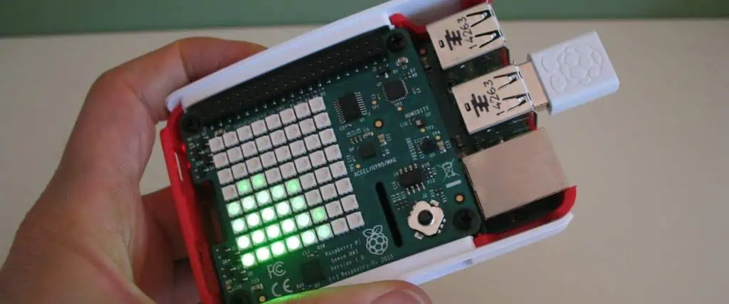
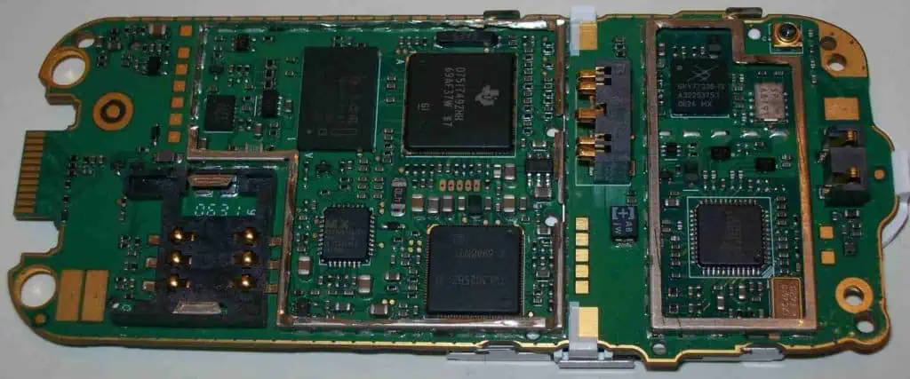
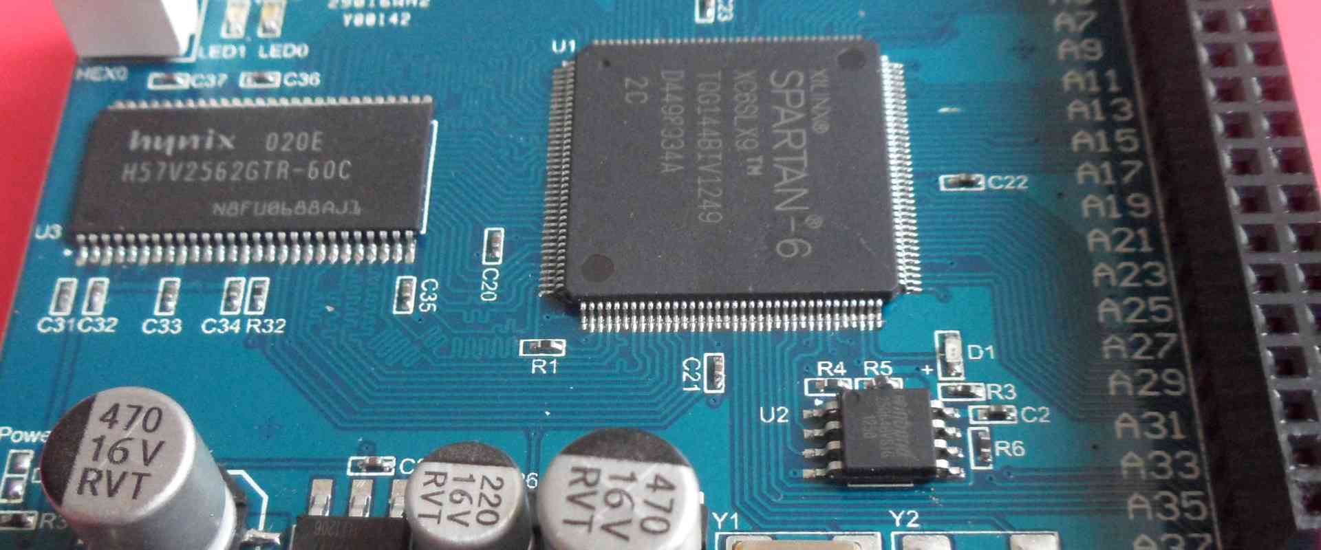
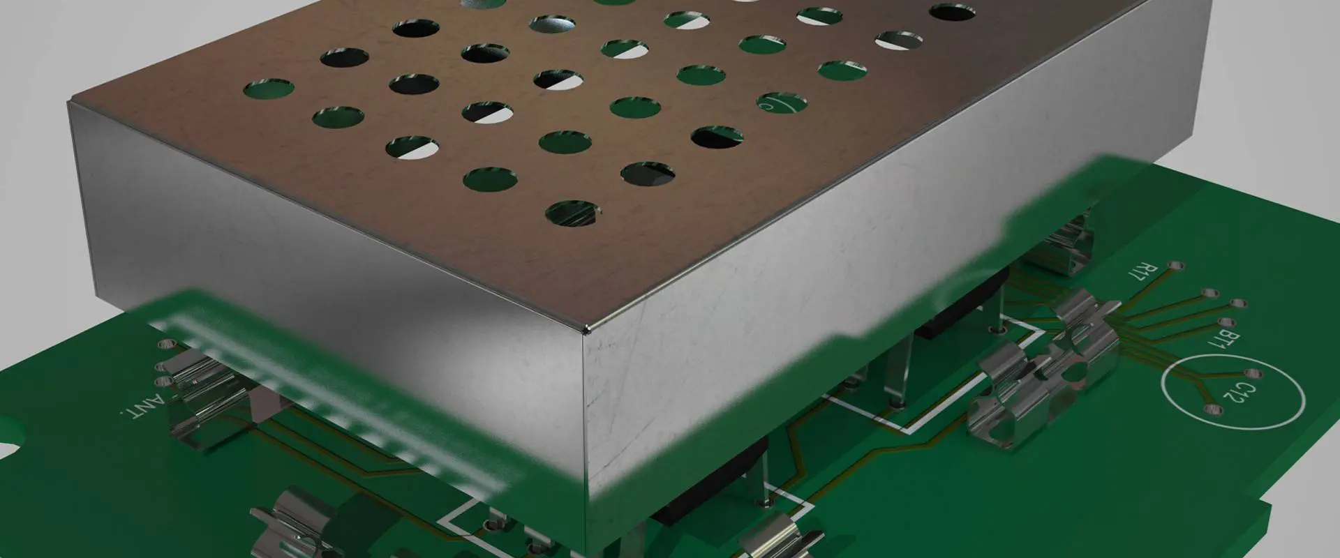
Board Level Shielding

Small metal cans soldered onto PCBs enclosing components needing isolation. Effective for blocking high frequency noise.

Cable Shielding

Foils or braided mesh surrounding cables that isolates signals from external noise pickup/radiation.

Component Shielding

Shielding integrated into component construction. Examples include metal core PCBs, shielded connectors, absorptive cables.

EMI Gaskets

Conductive elastomer gaskets placed between metallic chassis/covers that compress during closure to block EMI leakage through gaps.

Optimal shielding combines multiple techniques tailored to the frequency range, emissions sources, mechanical design and cost.

Shielding Materials

Materials commonly used for EMI shielding include:

  • Metals โ€“ Steel, nickel, copper, aluminium, tin
  • Conductive paints โ€“ Nickel/copper filled latex, epoxy, acrylic
  • Conductive coatings โ€“ Vacuum deposited aluminium on plastic
  • Conductive plastics โ€“ ABS, polycarbonate with Ni-coated graphite filler
  • Conductive foams โ€“ Silver coated open cell PU foam
  • EMI absorbers โ€“ Ferrite tiles, carbon loaded foam absorbers
  • EMI gaskets โ€“ Conductive elastomers with silver plating

Selecting suitable materials involves balancing shielding effectiveness, manufacturability, corrosion resistance, cost constraints and mechanical needs.

Shielding Design Considerations

Some key aspects for effective EMI shielding implementation are:

Governing Standards

  • Understand applicable emissions and immunity standards like FCC, CISPR 11

Frequency Range

  • Blocking lower frequencies requires thicker, solid metal shields unlike high frequencies

Shield Location

  • Close proximity to sources provides optimal containment

Seams and Gaps

  • Minimize openings for leakage of unwanted emissions

Grounding

  • Robust grounding of enclosure using multiple low impedance paths

Filtered Connectors

  • Prevent noise coupling through shields via connectors
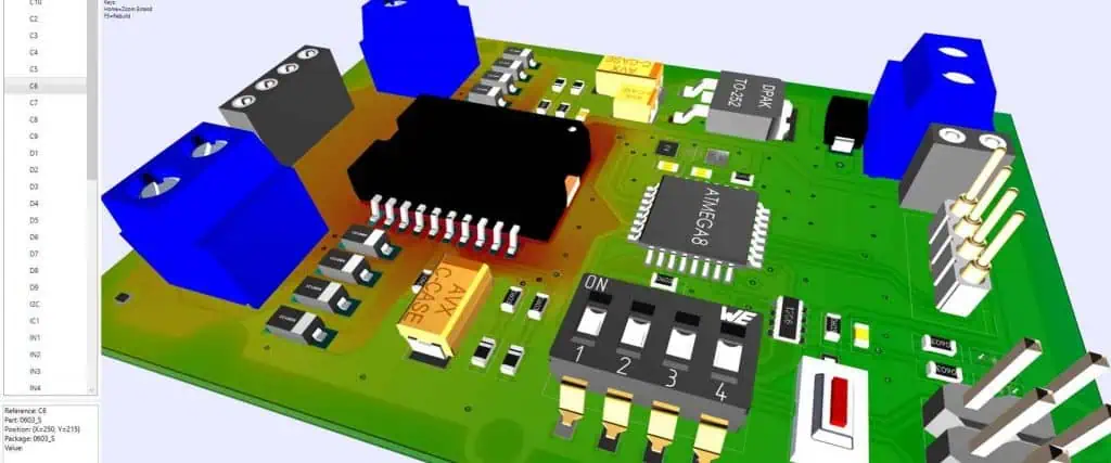
PCB Layout

  • Careful component placement, routing and stackups to isolate noise sources and victims

Simulation

  • Model shields and analyze with full-wave solvers to predict resonances

An optimized shielding system requires a holistic approach across mechanical, electrical and electronic design.

Shielding Performance Metrics

Shielding effectiveness indicates the reduction in radiated and conducted interference by shields and is expressed in dB. Key metrics are:

Plane Wave Shielding Effectiveness (PWSE)

Measures far-field attenuation when plane EM waves impact the shield. Important for emissions containment.

Near Field Shielding Effectiveness (NFSE)

Measures shielding performance for near-field electric and magnetic coupling. Crucial for immunity and signal isolation.

Transfer Impedance (ZT)

Determines conductivity across the shield between source and victim. Lower ZT indicates better absorption.

Insertion Loss

Measures the reduction in conducted interference from source to victim through shield. Similar concept as transfer impedance.

These parameters help evaluate material suitability and design robustness during shielding development. Shielding performance varies with frequency and needs to be validated across the spectrum.

EMI Shielding Measurement

Measuring the shielding effectiveness quantitatively helps assess design choices and improvements. Common measurement methods are:

Anechoic Chamber Testing

Full compliance testing method with antennas transmitting and receiving through the shielding barrier characterizing both plane wave and near field shielding. Provides wide frequency characterization in controlled lab environment.

GTEM Cell Testing

Uses a tapered septum transmission line to evaluate shielding effectiveness. Can test electric, magnetic and plane wave attenuation. Portable for spot measurements.

Shielded Box Method

Simple setup with noise generator and receiver placed inside and outside a shielded test enclosure to evaluate insertion loss at various points across frequency.

MESA Imaging

Scanning imaging system that maps emissions sources and propagation to pinpoint leakage points needing mitigation.

Validated measurements are crucial during prototyping to tailor the design before final compliance testing.

EMI Shielding Applications

EMI shielding is widely used in electronic products including:

Consumer Electronics

Laptops, smartphones, wearables, home appliances, game consoles

Automotive

Engine control units, infotainment systems, LIDAR modules

Aerospace

Avionics, flight control systems, communications

Medical

Monitoring equipment, implants, scanning systems

Instrumentation

Test and measurement equipment

Industrial

Automation controllers, motor drives, robotics

Communications

5G small cells, private networks, base stations

Any application where electronics need to operate reliably in noisy environments relies on EMI shielding principles implemented through careful mechanical, electrical and PCB design.

EMI Shielding Technology Trends

Advances in materials and manufacturing are expanding shielding capabilities:

  • 3D printing – Additively built metal enclosures with complex geometries
  • EMI paints – High aspect ratio carbon nanotubes for conductive coatings
  • Hybrid coatings – Composite paints combining copper and nickel for increased conductivity
  • Thin-profile shields – Flexible conductive tapes for tight space applications
  • Structural electronics – Shielding integrated into load bearing structures
  • MIT materials – Metamaterials, fractal geometries for improved absorption
  • Graphene composites – Graphene infused plastics for light yet effective shielding
  • AI-driven design – Optimizing shielding performance using simulations and generative design
  • Expanded applications – Effective shielding demands from electric vehicles, IoT endpoints and medical devices

With electronics getting more compact, efficient and operating at higher frequencies, shielding implementation is becoming more critical across application sectors.

Conclusion

As an indispensable technique for ensuring proper functioning and emission compliance of electronic equipment, EMI shielding encompasses specialized materials, design practices and measurements. Shielding methods from conductive coatings to faraday cages along with advanced materials like graphene and metamaterials provide a robust toolkit to contain radiated interference. With electronics advancement leading to increased interference susceptibility and emissions, shielding development using physics-driven modeling and AI-based design techniques promises to be a crucial competitive advantage for developing reliable, secured and compliant products.

What is EMI Shielding? – FQA

Q1. What is the purpose of EMI shielding in electronic products?

EMI shielding blocks electromagnetic interference from entering or escaping the device using conductive materials. This ensures proper functioning and meets EMC/EMI standards.

Q2. What are some common EMI shielding methods?

Shielding approaches include faraday cages, conductive coatings/plastics, board-level shields, cable shields, component shields, absorbers and EMI gaskets between metallic enclosures.

Q3. How is shielding performance quantified?

Key parameters are plane wave shielding effectiveness, near field shielding, transfer impedance and insertion loss. These determine attenuation across frequency spectrum.

Q4. What materials are commonly used for EMI shielding?

Materials used are metals like steel, nickel, copper, conductive paints, plastics, coatings, foams, absorbers, gaskets containing metallic fillers.

Q5. What are some considerations in EMI shielding design?

Considerations include applicable EMI standards, noise frequencies, shield location, seams/gaps minimization, grounding, filtered connectors, enclosure material and PCB layout techniques.

Xilinx XC7Z035-2FFG676i FPGA Price

Xilinx XC7Z035-2FFG676i

Xilinx XC7Z035-2FFG676i belongs to the Zynq-7000 family of FPGA. The architecture of the device is based on Xilinx SoC. This family of FPGA devices are integrating several features. The device is available in both double and single-core depending on the application for which it is used. The device is grounded on Xilinxโ€™s programmable logic or PS of 28nm. The device has an outstanding ARM Cortex A-9 processor that is considered the core of the device. Furthermore, these devices are having integrated on-chip memory, interfaces for peripheral connectivity, and external memory too.

Description of Processor

The processor of the Xilinx XC7Z035-2FFG676i is having four major blocks comprising the interconnects, input/output peripherals or IOP, memory interfaces, and the application processing unit or APU.

Application Processing Unit

FULL PCB MANUFACTURING Quote

The application processing unit of Xilinx XC7Z035-2FFG676i has several features such as it has single or dual-core ARM Cortex A-9 MP Cores. The ARM Cortex A-9 features comprise 2.5 DMIPS per MHz. The operational frequency range of the processor range from 667Mhz to 866Mhz for wire bond mode and flip-chip mode, it ranges from 667Mhz up to 1GHz. The APU has the capability of operating in a single processor, has dual modes for the asymmetric processor, and dual symmetric processor. The APU also has double and single precision floating points up to 2.0 MELOPS per MHz. There is a media engine known as NEON for the support of SIMD. The APU has support for the compression of code with its thumb-2. The level-1 caches are supporting separate data and instruction up to 32Kb each. The application processing unit is a four-way set associative. There is a built-in memory management unit, secure mode operation is handled with TrustZone. There is an eight-channeled DMA. The APU has support for multiple transfer types i.e., scatter-gather, peripheral to memory, memory to peripheral, and memory to memory.

Timers and Interrupts of Xilinx XC7Z035-2FFG676i

There are various timers and interrupts in the Zynq-7000 series of FPGA. The cross-trigger interface enables the triggers and breakpoints of hardware. There is trace support and CoreSight debug for Cortex A-9. For tracing and instruction, there is a program trace macro-cell. There are 2 triple counters and timers along 3 watchdog timers and a controller for general interrupt.

Memory Interfaces

The Xilinx XC7Z035-2FFG676i unit of memory interface comprises a controller for dynamic memory and an interface module for controlling static memory. The purpose of a dynamic memory controller is to extend support for DDR memories. The controller for static memory is extending support for interfaces of NAND flash, interface for NOR flash, parallel data bus, and an interface for Quad-SPI flash.

Dynamic Memory Interfaces of Xilinx XC7Z035-2FFG676i

The controller for DDR memory is multi-protocol and is being able to be configured for delivering wide access in 32 or 16 bits up to 1GB address space through the utilization of a unity rank configuration of 32, 8, or 16-bit memories of DRAM. There is dedicated 16-bit bus-access for the ECC support. The PS is incorporating associated PHY and controller for DDR comprising of its dedicated inputs/outputs. The speed support is up to 1333Mb/s for its DDR3 memory. The controller of the DDR memory is having the capability of multi-port and is enabling the system of processing a programmable logic in common access for shared memory. There is a total of 4 slave ports for the purpose to serve one as a 64-bit port that has dedicated use for the processor through the controller of level-2 cache and is configured for lower latency. For PL access, there are dedicated ports of 64-bit. There is a single 64-bit AXI-port that is common to all of the masters of AXI ports through a central interconnect.

Static Memory Interfaces of Xilinx XC7Z035-2FFG676i

The static memory interfaces of the Xilinx XC7Z035-2FFG676i are having support for external static memories as well. There is a data bus of 8-bit SRAM that can extend support to 64Mb. There is a NOR flash of 8-bit supporting till 64Mb.

Interconnects

There is a multi-layered interconnect in Xilinx XC7Z035-2FFG676i which is responsible for connecting IOP, interface unit of memory, APU, and PL. This interconnects supporting numerous master-slave transactions simultaneously and is non-blocking. The interconnect is fashioned in a way that it has latency for masters e.g., the master of ARM CPU is having displacement paths to reach memory and the masters that are bandwidth critical like PL masters are having higher throughput connection for slaves along the way they require to communicate. The regulation of traffic can be easily made through interconnecting with its QoS block. The QoS is featuring the regulation of traffic generated through CPU and DMA controllers.

Programmable Logic of Xilinx XC7Z035-2FFG676i

The key features of programmable logic or PL of the device include having a configurable logic block or CLB, 8 lookup tables in every CLB for distributed memory, and random logic implementation. The memory lookup tables are also configurable in two 32-bit block RAM or single 64-bit block RAM. These lookup tables can also be configured in the form of the shift register.  There are sixteen flip-flops through every CLB. There are two 4-bit adders in the cascaded mode for featuring arithmetic functions. The block RAM is of 36Kb.

Debug Ports

2 JTAG ports could be combined or utilized individually. Whenever combined, a single port is utilized for the ARM Cortex A-9 processor downloading of code and for the operations of run-time, PL debugs PL configuration and logic analyzer that is pro-embedded. This is enabling apparatuses like the software development kit of Xilinx and ChipScope Pro Analyzer for sharing a sole cable for downloading from the Xilinx database. Whenever JTAG ports are split, one of its ports is utilized for support of PS encompassing direct entree to the interface of ARM DAP. This interface of CoreSight is enabling the utilization of ARM acquiescent to correct and its software development tools like development studio 5. Other of the JTAG ports could be utilized by tools of Xilinx FPGA for accessing PL encompassing the downloads of bitstream configuration and PL debug along with the analyzer for integrated logic. This is the mode where workers could download and correct the PL in the form of separate FPGA.

Xilinx XC7Z020-1CLG484i Technical Data

Xilinx XC7Z020-1CLG484i

Zynq-7000 family of FPGAs have a lot of devices and Xilinx XC7Z020-1CLG484i is also one of them. These devices are built on the SoC architecture offered by Xilinx. The Zynq-7000 family is integrating abundant advanced features that its competitor devices lack. The device comes in either a single or dual-core ARM Cortex A-9 processor. The processing system of the device is grounded on the 28nm programmable logic introduced by Xilinx. The processing units are the integral part of the devices that also comprise built-in memory, interfaces for peripheral connectivity, and external memory.

The Xilinx XC7Z020-1CLG484i offers scalability and flexibility. It also delivers ease of use, power, and high performance that is associated with the ASSP and ASIC. These devices are very cost-sensitive and best suited to be used in higher performance applications from a common platform through the utilization of industry standards. Every device of the Zynq-7000 has input/output resources, PL, and PS but all features vary among devices depending on its use. There are abundant applications of Xilinx XC7Z020-1CLG484i and its family devices. For example, these devices are best to be used for driver assistance in the automotive industry, information delivery purposes to drivers, and in the infotainment of vehicles. These devices are preferred to be used in broadcasting cameras, motor control in industries, networking equipment of industries, and machine vision. The device is also utilized in smart and IP cameras. Recently, these devices were used in biomedical imaging and diagnostics, night vision, and video gadgets. Xilinx XC7Z020-1CLG484i is used in baseband and LTE radio sets and printers as well.

Interrupts and Timers

The device Xilinx XC7Z020-1CLG484i has numerous interrupts and timers. There is a controller for general interrupt. There are 3 watchdog timers i.e., each central processing unit has one watchdog timer. There are a couple of triple counters or timers. There is support offered for Cortex A-9 tracing and debugging of CoreSight. The device has a program trace macro-cell for tracing and instructions. The cross-trigger interface is enabling the deviceโ€™s triggers and hardware breakpoints.

The Input/Output Peripherals of Xilinx XC7Z020-1CLG484i

FULL PCB MANUFACTURING Quote

The input/output peripherals or IOP unit of the device has peripherals for data communication. There are abundant key features of the IOP unit such as having a couple of tri-mode 10/100/1000 peripherals for ethernet MAC having IEEE 802.3 and 1588 revision 2.0 standards. This unit has the capability of scatter-gather DMA, recognition support for 1588 revision 2 frames, and a couple of USB 2.0 peripherals each with 12 endpoints. There is support for the PHY interface along with support for full-speed and high-speed modes in on-the-go, device, and host configurations. There is an external PHY interface as well along with a couple of UARTs. There are 2 SPI ports of full-duplex mode along 3 peripheral chip selects.

External Interfaces for PS

The external PS interfaces of Xilinx XC7Z020-1CLG484i are utilizing certain dedicated pins that PL pins could not be assigned with. Such pins comprise the voltage reference, clock, boot mode, and reset pins. There are over 54 multi-use input/output pins along with software configurable pins for connecting either of the internal input/output peripherals along with controllers for static memory.

Phase-Lock Loop and Mixed-Mode Clock Manager

MMCM or mixed-mode clock manager and PLL or phase-lock loop of Xilinx XC7Z020-1CLG484i have numerous characteristics. Both PLL and MMCM could be served as the synthesizer of frequency for a large frequency range and also as a filter for jitter for all of the incoming clocks. The voltage-controlled oscillator is lying in the middle of both MMCM and PLL which is pacing up or slowing down depending on the voltage at its input from the phase frequency detector. A total of 3 programmable frequency dividers are there, namely O, M, and D. D is known as the pre-divider reducing the frequency at its input and feeding one input of conventional PLL frequency/phase comparator. M is known as a feedback divider acting like a multiplier as it is divider the output frequency of VCO before it is fed to other inputs of the phase comparator. M and D must be selected appropriately as it keeps the VCO following the required range of frequencies. There are 8 phases at the output of VCO equally spaced by 45ยฐ. There are 3 input-jitter filtering options in PLL and MMCM i.e., mode of lower-bandwidth having best jitter attenuation, higher bandwidth mode having best phase offset, and an optimized mode having tools for detecting the best setting.

Clock Management

The PS of Xilinx XC7Z020-1CLG484i is equipped with 3 PLLs that deliver the required flexibility in the configuration of clock domains through the PS region. A total of three main clock domains exists within PS. These clock domains comprise peripherals for input/output, controllers for DDR, and APU. The software tool can be utilized for configuring the frequencies of all of the domains.

Software and Hardware Debug Support

The architecture of ARM CoreSight is utilized for the debug system of Xilinx XC7Z020-1CLG484i. This architecture is utilizing components of ARM CoreSight comprising of embedded buffer trace, macro-cell for program trace, and instrument trace macro-cell. This is enabling the features of instruction trace along with triggers and hardware breakpoints. An integrated analyzer for logic can also be utilized for debugging the programmable logic.

Power Modes of Xilinx XC7Z020-1CLG484i

There are numerous power modes offered by Xilinx XC7Z020-1CLG484i such as the sleep or programmable logic power-off mode. Both PL and PS are residing on various power planes and PS is capable of running with PL being powered OFF. However, for security purposes, PL could not be powered ON before PS. PL is requiring reconfiguration after every power-ON state. Therefore, the users are supposed to consider the configurations of PL time whenever utilizing the mode of power-saving. There is a PS clock control mode. PS is capable of running even in reduced clock rates at around 30MHz through the use of internal phase-lock loops. Therefore, the clock rate could be changed dynamically. For dynamically changing the clock, the users are supposed to unlock the control register of the system for accessing the control register of the PS clock. There is a single processor mode too in which the 2nd cortex A-9 central processing unit is in turned-OFF mode through the use of clock gating and the 1st central processing unit is kept in operational mode.

Xilinx XC7Z015-1CLG485C Technical Parameter

Xilinx XC7Z015-1CLG485C

The Xilinx XC7Z015-1CLG485C device belongs to the Zynq-7000 series family and is grounded on the top-notch SoC architecture offered by Xilinx. These devices are integrating a single dual-core ARM Cortex A-9 state-of-the-art processor which is feature-rich. Moreover, these devices have outstanding processing systems based on 28nm programmable logic. The CPUs of the devices are considered processing system’s heart and are having memory integrated on-chip, interfaces for external memory, and interfaces for peripheral connectivity as well.

There are abundant features of the processing system of Xilinx XC7Z015-1CLG485C such as 2.5 DMIPS per MHz per central processing unit, the frequency of CPU can range up to 1GHz with support for coherent multi-processor. The architecture of the processing unit is based on ARMv7-A, security is of TrustZone along with instruction set of thumb-2. The environment of RCT execution is offered by Jazelle with the engine for media processing by NEON. The processing unit has interrupts and timers, 3 watchdog timers, a global timer, and 2 counters for the triple timer.  The cache of the device has support for byte parity, eight-way 512Kb set-associative cache of level-2, and four-way 32Kb set-associative level-1 data caches and instruction. There is a boot ROM on-chip, support for byte-parity, and RAM of 256Kb on-chip. Xilinx XC7Z015-1CLG485C has a multi-protocol memory controller for dynamic purposes, 16 or 32-bit interfaces for its DDR memories, and a 16-bit support mode for ECC. The device has an interface for static memory, support for NOR flash, address space of 1GB through the utilization of 32, 16, or 8-bit memories, and an 8-bit data bus for SRAM supporting up to 64MB.

The zynq-7000 series FPGA family is best suited for high bandwidth connectivity within PS and among PL and PS and has the support of QoS for critical matters for control of bandwidth and latency. The configurable logic blocks or CLBs of Xilinx XC7Z015-1CLG485C have lookup tables, adders cascaded together, and flip-flops. The block RAM of 32Kb is dual-port, supports up to 72 bits, and can also be configured as two parts in 18Kb. The DSP blocks have a pre-adder of 25-bit, an accumulator or adder of 48-bit, and a multiplier of 18×25. The PCI express of the device has support for endpoint configurations and root complex. It also has support for Gen2 speeds and 8 lanes. The transceivers are in serial mode and have about 16 transmitters and receivers with support up to data rates of 12.5Gb/s. There are a couple of 12-bit ADC or analog to digital converters having support for temperature and voltage sensing, have around 17 external input channels, and a conversion rate of up to one million samples every second.

Processor System

The processor system of Xilinx XC7Z015-1CLG485C contains four main blocks i.e., interconnects, peripherals for inputs/outputs, an application processing unit, and interfaces for memory.

Interfaces for Dynamic Memory

FULL PCB MANUFACTURING Quote

The controller of DDR memory which is multi-protocol could be configured for delivering 16 or 320bit accesses to the 1Gb address space through the utilization of unity rank configurations of 32, 16, or 8-bit DRAM memories.16-bit busses are utilized for support of ECC with the mode of bus access. PS is responsible for the incorporation of associated PHY and controller for DDR, comprising of its own input/output. The speed of the device could range to 1333Mb/s for its DDR3. The memory controllers of DDR memory are multi-port, capable of enabling the programmable logic and processing system for common access for shared memory and the controller of DDR is featuring 4 AXI ports in slave mode for the purpose.

Interfaces for Static Memory

The interfaces of the Xilinx XC7Z015-1CLG485C for static memory have support for static memories. The 8-bit data bus of SRAM is having the support of 64MB, 8-bit NOR flash is having the support of 64MB, and 1, 2, 4-bit SPI or a couple of quad-SPI serial NOR flash.

Accelerator Coherency Port

The ACP or accelerator coherency port of Xilinx XC7Z015-1CLG485Cย is 64-bit and has an interface of AXI slave providing connectivity among potential accelerator function and APU in PL. The ACP is connecting the PL and snoot control unit directly for the ARM Cortex A-9 processor that enables access for cache-coherence for the central processing unit’s data through both caches L1 and L2. ACP is also delivering a lower latency path among the PL and PS grounded accelerator whenever compared along with the legacy cache loading and flushing scheme.

The Programmable Logic of Xilinx XC7Z015-1CLG485C

The key features of the programmable logic of the device comprise configurable logic blocks or CLB and 8 lookup tables within every CLB for distributed memory or random logic implementation. The lookup tables are configurable in either one of 64-bit or two of 32-bit RAM. The lookup tables can also be configured as a shift register. There are 16 flip-flops in every CLB, a couple of 4-bit cascaded adders, block RAM of 36Kb that is 36-bit wide.

Electrical Characteristic

The outputs of Xilinx XC7Z015-1CLG485C that are single-ended are utilizing a traditional CMOS pull/push output structure that is driving it to a high state whenever towards VCCO and is driving it low whenever towards GND. The single-ended outputs can also be put to a z-state. The designer of the system is capable of specifying output strength and slew rate. The input is to be in an active state forever; however, it is often ignored whenever the output is in an active state. Every pin of the device may have an optional weak pull-down or pull-up resistor. Most pairs of signal pins can be terminated along with a 100 Ohms resistor.

System-Level Functions of Xilinx XC7Z015-1CLG485C

Various functions are spanning both PL and PS comprising reset management, device configuration, power management, clock management, along with support for software and hardware debugging.

Reset Management

The primary function of reset management is delivering the capability for the device to reset the device or even certain individual units within the device. The PS is having support for the signals and reset functions such as warm reset, reset for security violations or locked down reset, PL user resets, internal and external power-ON signal reset, reset for a watchdog timer, and resets for JTAG and software.

What is an Electronic Device?

Electronic Device

Introduction

An electronic device is equipment that operates by controlling the flow of electrons or other electrically charged particles in circuits, signal processors and other semiconductor devices. Electronic devices form the basic building blocks of complex electronic systems and play an indispensable role in our everyday lives.

This article provides a comprehensive overview of electronic devices including:

  • Definition and working principles
  • Classification based on application
  • Common components and materials used
  • Fabrication and assembly processes
  • Evolution and key milestones
  • Role and impact on society

Understanding the fundamentals of electronic devices is key to designing, manufacturing and leveraging electronics technology for benefit across industries.

What is an Electronic Device?

An electronic device is equipment that uses the controlled flow of electric charge carriers like electrons and holes in components like transistors, diodes, capacitors, resistors and inductors to process signals for implementing useful functions.

The key aspects that distinguish electronic devices are:

  • Use electricity – Electronic devices operate by controlling electricity in the form of currents and voltages rather than mechanical or optical means.
  • Semiconductor materials – They use semiconductor materials like silicon, germanium, gallium arsenide that enable control of conductivity for devices like transistors.
  • Discrete components – Individual components like transistors, ICs, resistors, capacitors, diodes and inductors fabricated from electronic materials.
  • Integrated circuits – Tiny microchips integrating thousands of electronic components like transistors and passive devices on semiconductor substrates.
  • Digital logic and processing – Devices use binary digital logic implemented through ICs to process signals and programmable operations.
  • Analog signal processing – Analog electronic circuitry handles continuously variable real-world signals like sound, images, radio waves.
  • Electron flow control – The basic operation involves controlled flow of electrons and holes in semiconductor devices.

This ability to leverage electron flow in miniaturized semiconductor components for computation, signal processing, communication and control purposes differentiates electronic devices from electrical or mechanical systems.

Classification of Electronic Devices

Electronic devices can be categorized based on their application and functionality into:

Consumer Electronics

  • Television
  • Radio
  • Smartphone
  • Laptop
  • Headphones
  • Fitness tracker
  • Smartwatch

Home Appliances

  • Washing Machine
  • Air Conditioner
  • Refrigerator
  • Microwave Oven
  • Vacuum Cleaner

Office Equipment

Industrial Electronics

  • Programmable Logic Controller
  • Process Control System
  • Robot
  • Motor Drive

Automotive Electronics

  • Engine Control Unit
  • Infotainment System
  • ABS System
  • Navigation System
  • Telematics Unit

Medical Electronics

  • ECG Machine
  • Ultrasound Scanner
  • Pacemaker
  • Blood Pressure Monitor
  • Microscope Camera

Test and Measurement

  • Digital Multimeter
  • Logic Analyzer
  • Spectrum Analyzer
  • Digital Oscilloscope
  • LCR Meter

IoT Devices

  • Smart Locks
  • Smart Lights
  • Smart Plugs
  • Security Cameras
  • Smart Sensors

From handheld gadgets to large industrial automation systems, electronic devices empower functionality and connectivity across diverse domains.

Electronic Device Components

Small Electronic Load PCBA Board

Electronic devices comprise of various components and materials that enable control and processing of electric currents and signals.

Semiconductor Materials

Materials like silicon, germanium, gallium arsenide used as substrates onto which semiconductor devices like diodes and transistors are fabricated.

Discrete Semiconductor Devices

Individual packaged diodes, transistors and thyristors that perform functions like rectification, amplification, fast switching.

Integrated Circuits

Microchips integrating thousands of transistors, diodes, resistors, capacitors on semiconductor wafers for implementing complex circuits.

Passive Components

Resistors, capacitors, inductors, transformers used for filtering signals, impedance matching, voltage division and energy storage.

Piezoelectric Materials

Piezoelectric crystals used in sensors, actuators and frequency control applications.

Magnetic Materials

Materials like ferrites, ferromagnetic alloys applied in inductors, transformers, coils, magnetic sensors.

Packaging

Plastic or ceramic packaging and interconnects housing the chip and providing terminals to connect to the external circuitry.

Printed Circuit Boards

Copper laminated boards providing mechanical structure and electrical interconnections between components.

Displays

LCD, LED displays that electronically modulate pixels to present visual information.

Sensors

Sensors like temperature, pressure, proximity, accelerometer that produce electronic signals representing physical phenomenon.

Power Supplies

AC-DC, DC-DC power converters delivering required stable, noise-free voltages.

Advances in these electronic component technologies enable development of ever more powerful and compact devices over the decades.

Electronic Device Fabrication

The core technologies used to fabricate electronic devices are:

Semiconductor Device Fabrication

Involves complex processes like photolithography, doping, etching, metallization done in specialized clean room environments to build up transistors and integrated circuits on silicon wafers.

PCB Fabrication

Involves laminating and etching multiple copper layers patterned using photoresist onto insulating substrates to create printed circuit boards.

Component Assembly

Attach discrete components onto PCBs using soldering techniques like wave soldering, reflow soldering and manual soldering.

Enclosure Fabrication

Plastic molding and metal stamping techniques used to fabricate outer casings to house the electronic sub-assemblies.

Product Integration

Individual sub-assemblies are put together including PCBs, displays, chassis, cables to assemble the final product.

System Validation

Extensive testing carried out to validate complete product functionality before shipment.

Leveraging improvements in these manufacturing processes has enabled increased sophistication, reliability and cost efficiency in electronics production.

Evolution of Electronic Devices

Electronic devices have evolved tremendously over the century through key milestones:

Vacuum Tubes

  • Early 20th century – Diodes and triodes open electronics era

Discrete Transistors

  • 1947 – Invention of bipolar junction transistor advances electronics

Integrated Circuits

  • 1958 – Integration of transistors revolutionizes electronics

Microprocessors

  • 1971 – Intel 4004 launches microprocessor revolution

Personal Computers

  • 1975 – Early PCs like Altair 8800 created

Mobile Phones

  • 1973 – First mobile handsets like Motorola DynaTAC released

Internet

  • 1983 – Internet adoption expands global connectivity

Smartphones

  • 2007 – Apple iPhone ushers the smartphone era

Internet of Things

  • 2009 – IoT connectivity accelerates growth of smart devices

Wearable Technology

  • 2015 – Consumer wearables like Apple Watch become popular

AI Acceleration

  • 2016 – AI chips increase penetration of machine intelligence

The relentless pace of miniaturization, advances in integrated circuits and wireless connectivity continue to fuel growth of innovative electronic devices.

Role and Impact of Electronic Devices

portable devices pcb

Electronic devices have deeply transformed society and the modern world through:

Computing Power

Providing exponential increases in computing power leading to the PC revolution and internet-based digital world.

Communications

Enabling real-time global wireless communications through smartphones and broadband networking.

Consumer Electronics

Driving extensive penetration of affordable and featured consumer electronics like TV, mobile, computers.

Automation

Industrial, home and office automation through sensors, robotics, control systems.

Biomedical

Improved healthcare access and diagnostics tools enabled by affordable medical electronics.

Sustainability

Driving energy efficiency, renewable energy adoption and circular economy through sensors and controls.

Research

Scientific research leveraging powerful electronic instrumentation, storage and computing.

Defense

Secure communications, precision weapons, avionics, radars for modern armed forces.

Space Technology

Satellite communications and spacecraft instrumentation.

Artificial Intelligence

Automating complex cognitive tasks through AI inferencing chips.

Electronic devices continue profoundly transforming industries and lives globally with increasing ubiquity across homes, enterprises, industrial systems and critical infrastructure. Future trends point to an era of ambient intelligence through the fusion of sensors, communications, AI and ubiquitous electronics.

Conclusion

Medical Devices pcb
Medical Devices pcb

Electronic devices encompass a broad range of equipment that process signals and accomplish useful functions by leveraging the controlled flow of electric charge through semiconductor materials and components. Ranging from discrete diodes and transistors to complex integrated circuits and embedded devices, electronics technology has been the major technological force shaping the modern digital world through exponential improvements in computing, communications, automation and connectivity. With electronics poised to become even more pervasive through concepts like IoT and edge intelligence, ongoing advances promise to reshape society in countless transformative ways in the decades ahead.

What is an Electronic Device? – FQA

Q1. What is the basic working principle of electronic devices?

Electronic devices operate by controlling the flow of electric charge carriers like electrons and holes in semiconductor materials and components for implementing useful functions.

Q2. What are the key components used in electronic devices?

Key components are semiconductor materials, discrete devices, ICs, passive components, piezoelectrics, magnetics, sensors, displays, interconnects and power supplies.

Q3. How are integrated circuits fabricated?

ICs involve complex fabrication processes like photolithography, doping, etching, metallization done in cleanroom environments to build up transistors and interconnects on semiconductor wafers.

Q4. What was the major milestone that enabled modern electronics?

The invention of the integrated circuit in 1958 allowed integrating multiple transistors into a miniaturized microchip, launching the electronics revolution.

Q5. What has been the impact of electronic devices on society?

Electronics have profoundly transformed society through computing, communications, automation, biomedical devices, defense systems, space technology and AI – making them indispensable for modern life.

What is Xilinx XC7K70T-2FBG484i FPGA ?

Introduction

The Xilinx XC7K70T-2FBG484i is a mid-range Kintex-7 series field programmable gate array (FPGA) by Xilinx featuring high performance, low power consumption and abundant resources for implementing digital circuits and systems.

This article provides an overview of the XC7K70T FPGA including:

  • Architecture and internal structure
  • Available resources and specs
  • Pinout and package details
  • Applications and use cases
  • Design considerations
  • Comparison with other Xilinx FPGAs

Understanding the capabilities and design factors for this versatile Kintex-7 FPGA enables leveraging it efficiently in various embedded, networking, industrial, automotive and interfacing applications needing programmable logic.

XC7K70T FPGA Architecture

Xilinx Artix 7
Xilinx Artix 7

The Xilinx XC7K70T belongs to the high performance mid-range Kintex-7 family built on a 28nm fabrication process. The FPGA architecture consists of:

Configurable Logic Blocks (CLBs)

  • Basic logic building blocks for implementing logic and arithmetic functions
  • Slice based architecture with two LUTs and two flip-flops per slice
  • 217,600 CLB slices, each with four 6-input LUTs and 8 flip-flops

Block RAM (BRAM)

  • 1020 dual-port 36 Kb block RAMs for on-chip data storage
  • Total 36.7 Mb memory
  • Configurable as single or dual-port RAM or ROM

DSP Slices

  • 360 DSP slices with 25 x 18 multipliers and 48-bit accumulators
  • High performance signal processing

Clock Management Tiles (CMTs)

  • 12 mixed-mode clock managers (MMCM)
  • Low jitter clock generation and frequency synthesis
  • Phase aligned clock division/multiplication

Multi-gigabit Transceivers (MGTs)

  • 16 serial transceiver blocks supporting up to 12.5 Gbps
  • Serializer/deserializer, clock correction, and data recovery

Input/Output Blocks (IOBs)

  • High speed selective I/O supporting standards like LVCMOS18, LVDS, HSTL

PCI Express Block

  • Gen2 x8 lane PCIe interface block

This combination of flexible CLBs, abundant memory, DSP slices, clocking, high-speed transceivers and I/O enables implementing a wide range of system-level functionality on the XC7K70T FPGA.

XC7K70T-2FBG484i Resources and Specifications

The commercial grade XC7K70T-2FBG484i device has the following key features and resources:

Logic Cells

  • 217,600 CLB slices with 6-input LUTs and flip-flops

Block RAM

  • 1020 x 36 Kb block RAM bits
  • Total 36.7 Mb

DSP Slices

  • 360 DSP slices with 25×18 multipliers

Transceivers

  • 16 x 12.5 Gbps transceiver channels

Maximum User I/O

  • 378 I/O pins

Clock Management Tiles

  • 12 MMCM and 13 DCM blocks

PCI Express

  • Gen2 x8 lane endpoint block

Memory Interface

  • DDR3, DDR2, LPDDR2, DDR controller blocks

Configuration

  • 667 Mb/sec SelectMAP interface
  • JTAG, SPI and BPI flash loading

Power Consumption

  • Maximum junction temperature of 100ยฐC
  • 10 W typical power

The abundant programmable resources enable implementing a wide range of complex digital systems leveraging the high speed, low power and small form factor benefits of the Kintex-7 FPGA.

XC7K70T Pinout and Package

The XC7K70T-2FBG484i comes in a 484 pin fine-pitch BGA package with dimensions of 23×23 mm offering a compact footprint.

The BGA484 package ball positions are shown below:

XC7K70T BGA484 package and pinout (Source: Xilinx)

The pins include:

  • 180 signal I/O pins
  • 16 transceiver lanes over 32 differential pairs
  • 150 power and ground pins
  • JTAG pins for debug and configuration
  • Clock pins for various clock inputs
  • DDR memory interface pins
  • Quad-SPI flash pins
  • PCIe interface pins

This high density pinout enables connecting to a large number of external signals for interfacing the XC7K70T FPGA to other devices.

Applications of XC7K70T FPGA

With its blend of programmable logic, memory, DSP, transceivers and interfaces, the Xilinx XC7K70T FPGA is well suited for a wide range of applications including:

  • Wired communications โ€“ Telecom protocols, encryption, network processors
  • Wireless infrastructure โ€“ Baseband processing, MAC, PHY layer
  • Automotive โ€“ ADAS, vision systems, engine control units
  • Industrial โ€“ Motor drives, robotics, Industry 4.0 systems
  • IoT and edge computing โ€“ Signal processing, sensor aggregation
  • Video and imaging โ€“ Encoder/decoder, codecs, filters
  • Medical โ€“ Diagnostic systems, ultrasound, tomography
  • Aerospace and defense – Navigation, guidance systems
  • High performance computing โ€“ Algorithm acceleration

For small form factor embedded applications needing FPGA programmability, the XC7K70T provides a compelling solution. The low power consumption enables battery operated portables and handheld devices as well.

XC7K70T Design Considerations

Xilinx FPGA distributor

To effectively harness the capabilities of the Xilinx XC7K70T FPGA, designers should keep in mind:

Team Expertise

  • Prior experience with Xilinx 7-Series FPGAs recommended
  • Proficiency with Vivado Design Suite tools and flows

Cooling

  • Max junction temperature is 100ยฐC
  • Utilize heat sinks, airflow for cooling in high power use cases

Pin Planning

  • Map external interfaces and connections to suitable pins
  • Plan for clocking, power schemes early

IP Integration

  • Xilinx Core Generator and IP catalogue enables integrating blocks for PCIe, Ethernet, Interlaken etc.

Simulation

  • Verify functionality through Vivado simulation before implementation

Team Collaboration

  • Use RTL source control and incremental team development

Accounting for thermal design, simulation needs, IP integration strategies early in the development cycle enables capitalizing on the XC7K70T capabilities for targeted application requirements.

XC7K70T vs other Xilinx FPGAs Comparison

XC7K70T vs XC7K160T

  • The XC7K160T offers higher capacity with ~1.5x more CLB slices
  • 16x 12.5 Gbps transceivers same as XC7K70T
  • Package options up to 780 pin count vs 484 pin for XC7K70T
  • XC7K160T suited for more complex logic, higher pin count needs

XC7K70T vs XC7K325T

  • XC7K325T has much higher capacity – almost 3x more CLB slices
  • 25x more BRAM blocks and 2.5x more DSP slices compared to XC7K70T
  • 28x 12.5 Gbps transceivers, 686 user I/O pins
  • XC7K325T fits very dense logic, high speed applications

XC7K70T vs Artix-7 100T

  • Artix-7 is low-cost, low power optimized family
  • XC7K70T has 4x more CLB slices than 100T; also more BRAM and DSP
  • Both have 16 transceivers; XC7K70T offers faster 667 Mb/s configuration
  • XC7K70T suited for more complex logic and performance needs

XC7K70T vs Zynq 7020

  • Zynq 7020 combines Cortex-A9 ARM cores with programmable logic
  • 7020 has 85k logic cells vs 217k in XC7K70T but adds dual core CPU
  • 7020 has 2.5x less BRAM; both have 16 transceivers
  • Zynq best suited for processing+logic applications vs pure FPGA needs

The Xilinx XC7K70T hits a sweet spot between capability and cost for mid-range applications compared to smaller or larger 7-series FPGAs.

Conclusion

The Xilinx XC7K70T FPGA provides an optimal blend of high performance programmable logic fabric along with abundant memory, DSP, transceivers, PCIe, memory interfaces and I/O in a power-optimized low cost package.

The Kintex-7 based architecture enables implementing a wide gamut of embedded, connected and high speed systems for applications across communications, industrial, automotive, datacenter and interfacing domains.

Adopting suitable design practices in terms of thermal management, pin planning, simulation, IP integration and expert design flows enables fully harnessing the XC7K70T capabilities for accelerated development.

What is Xilinx XC7K70T-2FBG484i FPGA? – FQA

Q1. What FPGA family does the Xilinx XC7K70T device belong to?

The XC7K70T is a member of the mid-range Kintex-7 family of FPGAs featuring high performance and low power consumption.

Q2. What are the key components in the architecture of the XC7K70T FPGA?

Key components are the CLB slices, 36Kb BRAM blocks, DSP slices, clock management tiles, multi-gigabit transceivers and flexible I/O blocks.

Q3. What applications is the XC7K70T FPGA suitable for?

It suits applications like telecom, wireless, automotive, industrial, imaging, defense, HPC needing mid-density programmable logic.

Q4. What package is used for the XC7K70T-2FBG484i device?

It uses a fine-pitch 484-pin BGA package to provide a compact 23x23mm footprint with 16 transceiver lanes.

Q5. How does the XC7K70T compare to the higher density 7-series XC7K325T FPGA?

The XC7K325T offers 3x higher programmable logic capability, 25x more BRAMs along with more transceivers and I/O suited for very complex designs.

What is Xilinx XC7A100T-2FGG676i FPGA?

Xilinx XC7A100T-2FGG676i

Introduction

The Xilinx XC7A100T-2FGG676i device is a high performance FPGA (Field Programmable Gate Array) belonging to the Artix-7 family. With its abundant programmable logic, memory, DSP, and transceiver resources, the XC7A100T FPGA is well suited for networking, wireless, aerospace, medical, and video processing applications needing medium-to-high capacity programmable hardware.

This article explores the XC7A100T FPGA architecture, available resources and configurations, design considerations, comparison with other FPGAs and target applications which helps assess its fit for different projects.

XC7A100T FPGA Architecture

The Xilinx XC7A100T FPGA is fabricated using a 28nm process and is based on the Artix-7 FPGA architecture which consists of the following key components:

Configurable Logic Blocks (CLBs)

  • The basic logic building block comprising of Look-Up Tables (LUTs), flip-flops and multiplexers
  • The XC7A100T has 115,200 CLB slices, with each slice containing 4 LUTs and 8 flip-flops

Block RAM (BRAM)

  • 16.2 Mb of total BRAM for on-chip data storage
  • Usable as 36 Kb true dual-port or 72 Kb simple dual-port blocks

Digital Signal Processing (DSP) Slices

  • 240 DSP slices with 25 ร— 18 multipliers for high-speed arithmetic

Clock Management Tiles (CMTs)

  • 8 Clock Management Tiles (CMTs) consisting of MMCMs and PLLs for clock synthesis

Input/Output Blocks (IOBs)

  • Programmable high-performance SelectIOTM interface blocks
  • Support common I/O standards like LVCMOS, LVDS

Transceivers

  • Integrated multi-gigabit transceivers with data rates up to 12.5 Gbps

This combination enables implementing wide range of complex digital interfaces, processing and control systems using the Artix-7 family architecture.

XC7A100T-2FGG676i Features and Specifications

The key features and resources available in the XC7A100T-2FGG676i FPGA variant are:

Logic Cells

  • 115,200 CLB slices
  • 460,800 LUTs, 921,600 Flip-flops

DSP Slices

  • 240 DSP48E1 slices

Block RAM

  • 16.2 Mb distributed RAM
  • 216 x 36 Kb blocks

Transceivers

  • 6 x 12.5 Gbps transceiver channels

Maximum User I/O

  • 413 I/O pins

Clock Management

  • 8 MMCM, 12 PLL blocks

PCI Express

  • Single PCIe Gen2 x1 lane endpoint

This combination makes the XC7A100T suitable for applications like wireless communications, medical imaging needing moderate programmable logic performance along with high-speed serial connectivity.

XC7A100T Design Considerations

Some key considerations when working with the XC7A100T-2FGG676i FPGA include:

Tool Flow – Xilinx Vivado tools for synthesis and implementation

Simulation – Vivado simulator, ModelSim for verifying functionality

IP Integration – Xilinx IP catalog provides various interface, processing cores

Pin Planning – Mapping system interfaces and I/O to FPGA during design entry

Clocking – Leveraging MMCMs and PLLs for synthesis and jitter control

Transceiver Design – Following Xilinx transceiver wizard and routing guidelines

Team Experience – Prior expertise with Artix-7 architecture recommended

Taking these factors into account early in the design cycle enables fully harnessing the powerful capabilities of the XC7A100T FPGA.

XC7A100T Target Applications

The Artix-7 based XC7A100T FPGA is suitable for a wide range of applications including:

  • Wireless communications – Radio and baseband processing, wireless microcells
  • Aerospace and defense – Navigation systems, avionics, image processing
  • Test and measurement – High-speed control and analysis
  • Medical – Ultrasound, tomography, DNA sequencing systems
  • Video broadcasting – Encoder/decoder systems
  • Wireline access – Ethernet switches, programmable networking
  • Automotive – Advanced driver assistance systems, infotainment
  • Industrial – Process control systems, instrumentation
  • High performance computing – Hardware acceleration, algorithm offload

The transceivers, DSP blocks and abundant programmable logic enable implementing processing intensive and high-speed interfacing systems optimized for these domains.

XC7A100T vs Other Xilinx FPGAs

XC7A100T vs Artix-7 35T

  • 35T FPGA has about 70% of the programmable logic resources
  • Reduced transceiver channels and smaller form-factor 256 pin package

XC7A100T vs Kintex-7 100T

  • Kintex-7 100T has similar capacity but higher performance minutes
  • Adds memory, PCIe Gen 3, QSFP interface capabilities

XC7A100T vs Spartan-7 100

  • Spartan-7 100 has 40% less capacity than Artix-7 100T
  • Maximum speed grade of -2, no transceivers

XC7A100T vs Zynq-7000

  • Zynq combines FPGA programmable logic with dual-core ARM CPU
  • Well suited for processor acceleration vs pure FPGA applications

The XC7A100T offers compelling programmable logic capacity and high-speed transceivers for the Artix-7 mid-range class.

Conclusion

Xilinx FPGA distributor

The Xilinx XC7A100T-2FGG676i FPGA packs 460K logic cells, 240 DSP slices and 6 integrated 12.5G transceivers that make it suitable for communication systems, image processing, test equipment and other applications demanding reasonably high logic capacity and serial connectivity. The availability of a rich set of IP, software tools and documentation enables rapid development leveraging the Artix-7 family. Engineers can fully utilize the potential of this FPGA for creating high-performance systems by following design guidelines outlined for Artix-7 devices.

What is Xilinx XC7A100T-2FGG676i FPGA? – FQA

Q1. What applications is the Xilinx XC7A100T FPGA well suited for?

The XC7A100T with 460K logic cells, 240 DSP Blocks and high-speed transceivers fits well for wireless, aerospace, medical imaging, video broadcasting and test applications.

Q2. What FPGA family does the XC7A100T device belong to?

The XC7A100T is a member of the mid-range Artix-7 family of FPGAs featuring optimized programmable logic fabric and high-speed serial connectivity.

Q3. How does the XC7A100T resource capacity compare with higher-end Kintex-7 FPGAs?

The XC7A100T has similar programmable logic capacity as Kintex-7 but lower performance, less memory, and lacks PCIe Gen 3 and QSFP blocks featured in high-end Kintex-7.

Q4. What are some key components in the XC7A100T FPGA architecture?

Major components are the 460K 6-input LUT logic cells, 16 Mb BRAM blocks, 240 DSP48E1 slices, integrated 12.5G transceivers and high-range SelectIO interface blocks.

Q5. What expertise is recommended for designing with the XC7A100T FPGA?

Prior experience with Xilinx tools and Artix-7 architecture is beneficial. Simulation, pin planning, transceiver and clocking design skills are key for harnessing XC7A100T effectively.

Xilinx XC7A35T-2CSG325i FPGA

Xilinx XC7A35T-2CSG325i

The Xilinx XC7A35T-2CSG325i device belongs to the Xilinx-7 series family of FPGAs that is addressing the wide range of requirements of the system. The requirements range from higher volume applications, logical capacity, smaller form factor, low cost up to ultra-higher bandwidth for abundant higher-performance applications. This family of FPGAs is comprising of Kintex-7, Virtex-7, Spartan-7, and Artix-7devices.

Spartan-7 devices are designed for low-cost optimization, lower power consumption, and higher input/output performance. These devices are available in lower-cost, minor form-factor packaging bearing a minor PCB footprint. The Artix-7 devices are designed for applications that consume less power, require the use of serial transceivers along with higher logical throughput and higher DSP. These devices are offering lower costs for the bill of material for cost-sensitive applications. The Kintex-7 devices are designed for achieving the best price-performance along with double improvements when compared to its competitor devices developing a novel FPGAs class. The Virtex-7 devices are designed for achieving the higher performance of the system along with double capacity improvement for the performance of its system. The device’s higher capability is enabled with the technology of stacked silicon interconnect.

Summary of Xilinx XC7A35T-2CSG325i

FULL PCB MANUFACTURING Quote

The Xilinx XC7A35T-2CSG325i device is capable of innovative FPGA logic that bears high performance and is grounded on the 6-inputs lookup table which can be configured in the form of distributed memory. There is a block RAM of size 36KB with integrated FIFO logic for buffering the data on the chip. The device is having its higher performance SELECTIO technology supporting the DDR3 interface with a size of around 1866MB/s. The serial connectivity of the device is a high speed and has an integrated transceiver of multi-gigabit that ranges from 600Mb/s to 6.6Gb/s and offers a dedicated optimized low-power mode for its all interfaces on the chip. There is an analog interface that is user-configurable incorporating a 12-bit dual MSPS converter (analog to digital) along with an integrated thermal sensor. Xilinx XC7A35T-2CSG325i has clock management tiles or CMT that are powerful and integrating both mixed-mode clock manager and phase-lock loop for achieving lower jitter and higher precision. The device is having an embedded MicroBlaze processor.  

SSI (Stacked Silicon Interconnect) Technology of Xilinx XC7A35T-2CSG325i

Several challenges are related to the creation of FPGAs with higher capacity that Xinlix is currently addressing through its SSI technology. This technology is enabling the multiple logic regions to be integrated along with a layer that is passive interposer through the use of proven assembly and manufacturing facilities from the leaders of industry for creating an FGPA having over 10 thousand SLR connection to provide connectivity of higher bandwidth along maintaining lower latency and consume less power. Two different types of SLRs are utilized in the Virtex-7 series of FPGAs. One of the SLRs is logic intensive that is utilized in the T-devices and SLR that is block RAM, DSP, or transceiver-rich is utilized in the HT and XT-devices. The SSI technology is enabling the production of FPGAs that have the highest capacity when compared to conventional methods of manufacturing that enable the higher performance and capacity FPGAs created for reaching to production phase rapidly with lower risks.

Distribution of Clock

The Xilinx XC7A35T-2CSG325i devices are offering a total of 6 dissimilar kinds of clock lines. The clock lines are names BUFMR, BUFG, BUFH, high-performance, BUFIO, and BUFR. All of these clock lines are for addressing the requirements of clocking for getting minor propagation delay, highest fanout, and low skew.

Xilinx XC7A35T-2CSG325iโ€™s Global Clock Lines

The Xilinx XC7A35T-2CSG325i devices is having a total of 32 global clock lines that are having the higher fanout that is reaching the flipflop clock, logic inputs, reset/set pins, and clock enable too. A total of twelve global clock lines are there residing within the clock region that drives through the clock buffers lying horizontally designated as BUFH. Every BUFH is capable to be disabled or enabled independently which allows turning OFF of the clocks through a specific region offering fine-grain control through which the regions of the clock are consuming power. The global clock lines are capable to be driven through global clock buffers that are allowing a glitch-free performance of the multiplexing of the clock along with other functions of the clock enable. Global clock lines can also be configured and driven from the configuration management tiles that is eliminating the delay of clock distribution.

Regional Clocks of Xilinx XC7A35T-2CSG325i

The regional clocks are capable of driving all of the clock destinations within their regions. The region is elaborated as the area having 50 of the input/output and 50 of CLBs. The Xilinx XC7A35T-2CSG325i devices are having about 2 to 24 regions in total. A total of 4 tracks of regional clock are in each region. Every buffer of regional clock could be driven through any of its 4 pins for clock-capable function at the input and their frequency could also be optionally divided with an integer that ranges from 1 to 8.  

Correction and Detection of Errors

Every of the 64-bits block RAM of Xilinx XC7A35T-2CSG325iย is capable of generation, storage, and utilization of 8 hamming code bits. The block RAM is also capable of performing error correction of single-bit and error detection of double-bit while the process of reading is in progress. The error correction and detection logic are also utilized whenever reading from or writing to the memories that are 64 to 72 bits wide.

Out-of-Band Signaling

The transceivers of the device Xilinx XC7A35T-2CSG325i are offering the out-of-band signaling that is utilized whenever sending lower speed signals from transmitter to that of receiver when the rapid transmission of serial data is not active. This is conventionally done whenever the link is at the power-down condition and is not adjusted.

Partial Reconfiguration, Readback, Encryption

The entire Xilinx-7 FPGA series with an exception of XC7S15 and XC7S6, bitstreams of FPGAs are containing sensitive consumer IP. This consumer IP is protected with AES encryption having 256-bit along with SHA-256/HMAC verification for prevention of illegal duplication of design. These FPGAs are performing decryption while the configuration is in progress with the help of a 256-bit key that is stored internally. Abundant of the configuration data could be read-back without having an impact on the operation of the system. Conventionally, the configuration is considered as the all-or-nothing operation; however, in the Xilinx-7 series family, the FPGAs are supporting partial reconfiguration. This feature is flexible and powerful too allowing the users to alter a certain portion of the device, keeping other portions in static condition.

What is Xilinx XC6SLX16-3CSG324i FPGA?

Xilinx XC6SLX16-3CSG324i

Introduction

The Xilinx XC6SLX16-3CSG324i device is a low-power, medium-capacity FPGA (Field Programmable Gate Array) belonging to the Spartan-6 family. With its combination of logic cells, memory, DSP blocks and high-speed I/O, the XC6SLX16 FPGA provides a versatile solution for networking, industrial, consumer and embedded applications.

This article provides an overview of the XC6SLX16-3CSG324i FPGA architecture, available resources, design considerations, key capabilities and target applications which helps designers evaluate its suitability for different project needs.

XC6SLX16 FPGA Architecture

The Xilinx XC6SLX16 FPGA is fabricated on a low-power 45nm process and is based on the Spartan-6 architecture which consists of the following main blocks:

Configurable Logic Blocks (CLBs)

  • The main logic resource consisting of look-up tables (LUTs) and flip-flops
  • XC6SLX16 has 10,320 CLB slices, with each slice containing 4 LUTs and 8 flip-flops

Block RAM (BRAM)

  • 148 Kb of fast dual-port block memory suitable for data storage
  • Configurable as 36 Kb memory blocks

Digital Signal Processing (DSP) blocks

  • 16 DSP48A1 slices with 25 x 18 multipliers and 48-bit adders
  • Enables high-performance arithmetic and signal processing

Input/Output Blocks (IOBs)

  • 240 High-speed I/O pins with support for common I/O standards
  • Features like differential signaling and PLLs for source synchronous interfacing

Clock Management Tiles (CMTs)

  • 4 Mixed Mode Clock Managers (MMCM) for clock synthesis, skewing, jitter filtering

PCI Express Interface

  • PCI Express Endpoint block enabling PCIe 1.1 connectivity

This combination of flexible fabric along with hardened IP blocks enables implementing a wide range of system-level functionality leveraging the Spartan-6 architecture.

XC6SLX16-3CSG324i Features and Specs

The key features and specifications of the XC6SLX16-3CSG324i FPGA are highlighted below:

Logic Cells

  • 10,320 CLB slices
  • 41,280 LUTs, 82,560 Flip-flops

DSP Slices

  • 16 DSP48A1 slices

Block RAM

  • 148 Kb
  • 36 18Kb blocks

Transceivers

  • No transceivers

Maximum User I/O

  • 240 pins

Clock Management

  • 4 MMCM, 10 DCM blocks

PCI Express

  • Single x1 lane endpoint

Memory Interfaces

  • DDR, DDR2, LPDDR controllers

Configuration

  • SelectMAP 8-bit, JTAG interfaces
  • SPI serial flash loading

The XC6SLX16 delivers an optimal balance of programmable logic, built-in blocks and high-speed I/O to address a wide range of applications.

Design Considerations with the XC6SLX16

Some key considerations for designers working with the XC6SLX16-3CSG324i FPGA include:

Tool Flow – Xilinx ISE tools for synthesis, place and route. ModelSim for simulation

Power Analysis – Analyze power consumption early in the design process

Pin Planning – Planning I/O configuration and assignments

Board Design – Following reference design layout guidelines

IP Selection – Adding relevant IP cores from Xilinx IP library

Team Skills – Prior experience with Xilinx Spartan-6 architecture is beneficial

Applications of XC6SLX16 FPGA

Some of the major application areas where the XC6SLX16 FPGA fits well are:

  • Embedded systems – Industrial automation, robotics, medical equipment
  • High speed interfacing – Video, imaging, high-performance computing
  • Wired communications – Data processing, algorithm acceleration, encryption
  • Wireless infrastructure โ€“ DAS, small cell radio processing
  • Analog and mixed signal – Protocol bridging, sensor interfaces
  • Automotive – Body electronics, instrument clusters, diagnostics
  • Security systems – Surveillance, access control, authentication
  • IoT – Gateway processing, sensor aggregation, edge computing

The Spartan-6 architecture provides a higher performance, low cost, power efficient solution for cost-sensitive applications compared to CPLDs or microcontrollers.

XC6SLX16 vs Other Xilinx FPGAs

Xilinx FPGA distributor

Some comparisons with other Xilinx FPGAs are:

XC6SLX16 vs XC7S15

  • XC7S15 belongs to a newer higher performance Artix-7 family
  • Similar logic capacity but XC7S15 adds DSP blocks and transceivers

XC6SLX16 vs XC7A50T

  • XC7A50T has twice the logic capacity with similar DSP blocks
  • Adds integrated transceivers, DDR3 interfacing

XC6SLX16 vs CoolRunner-II CPLD

  • CoolRunner-II has very low power consumption
  • But far lower logic density than XC6SLX16 FPGAs

XC6SLX16 vs Zynq-7000

  • Zynq combines Cortex-A9 ARM cores with programmable logic
  • Ideal for processor acceleration applications vs pure FPGA needs

The XC6SLX16 strikes a balance between capability and cost for mid-range applications compared to CPLDs or high-end FPGAs.

Conclusion

The Xilinx XC6SLX16-3CSG324i combines a powerful blend of 41k logic cells, 36Kb RAM blocks, 240 I/O pins, and high speed connectivity in a low power, small form factor FPGA. The Spartan-6 family enables the right mix of performance and cost efficiency for a wide gamut of embedded systems, wired communications, image processing, automotive and other applications. By following recommended design practices, engineers can fully harness the potential of this versatile mid-range FPGA.

What is Xilinx XC6SLX16-3CSG324i FPGA? – FQA

Q1. What is the Xilinx XC6SLX16-3CSG324i FPGA?

The XC6SLX16-3CSG324i is a low-power, medium-density FPGA from the Xilinx Spartan-6 family featuring over 10K logic slices and 240 I/O pins.

Q2. What are the key components in the XC6SLX16 architecture?

The key components are the configurable logic blocks for implementation of logic, 36Kb RAM blocks for data storage, DSP slices for signal processing and high-speed mixed-signal I/O.

Q3. What applications can the XC6SLX16 FPGA be used for?

This FPGA suits applications like industrial automation, video systems, wired communications, automotive body electronics and IoT edge computing needing mid-capacity programmable logic.

Q4. How does the XC6SLX16 compare with the higher-end XC7A50T FPGA?

The XC7A50T has double the programmable logic capacity along with high-speed transceivers and DDR3 interfacing making it suitable for more complex applications.

Q5. What are some key design considerations for the XC6SLX16 FPGA?

Important considerations are proper tool selection, power analysis, I/O pin planning, following reference designs, leveraging IP cores and having experience with Spartan-6 architecture.

PCB Assembly (PCBA) Design Guide

pcba design

Introduction

PCB assembly or PCBA refers to the manufacturing process where electronic components are mounted and soldered onto a printed circuit board to realize an electronic device or system. Implementing an optimized PCBA design flow is crucial for assembling PCBs that meet all functionality, reliability and quality requirements cost-effectively.

This guide provides a comprehensive overview of best practices and key considerations across the PCBA design stages:

  • Component selection
  • PCB footprint design
  • Placement considerations
  • Routing
  • Thermal design
  • Post-assembly inspection
  • Manufacturing guidelines

Following these PCBA design principles and strategies will help achieve optimized manufacturability, yield and performance.

Component Selection

Choosing the right components is the first step in PCBA design. Key guidelines for component selection are:

  • Functionality – Components must meet all technical specifications in terms of functionality, electrical ratings, tolerance, frequency response etc.
  • Availability – Select industry standard components that will be available through multiple suppliers and long lifetime.
  • Cost – Balance performance needs with component costs and pricing trends. Consider lower cost equivalents.
  • Supplier – Prefer reputable authorized suppliers over unknown third-party component vendors.
  • Packagingย – Give preference to surface mount packages for ease of assembly. Avoid outdated leaded packages.
  • Lifecycle – Choose components that are not nearing end-of-life status or select alternate replacements.
  • Counterfeits – Insist on parts from authorized distributors to avoid fake components.
  • Environment – Select RoHS compliant lead-free components suited to the operating environment.
  • Parametric Search โ€“ Leverage vendor component databases like Digikey, Mouser for parametric searching.

Careful component selection right at the design stage sets the foundation for a smooth PCBA process.

PCB Footprint Design

Footprint in PCB

The PCB footprint or land pattern refers to the copper pads and traces on the board providing the electrical and mechanical interface for soldering components. Good footprint design ensures reliable solder joints. Key aspects:

  • Datasheet recommendations – Follow datasheet specifications for pad dimensions, layout and thermal reliefs.
  • Package type – Tailor footprint layout for the component package – QFP, SOP, BGA etc.
  • Dimensioning – Account for factors like mask alignment tolerance, solder mask expansion, hole drilling accuracy.
  • Pad shape and size – Appropriate for leads or balls, allow for tolerances and solder coating.
  • Paste masks – Define suitable solder paste areas for formation of correct joints.
  • Thermal relief – Include ground plane cutouts under pads for heat dissipation during soldering.
  • Annular rings – Ensure recommended pad overlap with drill holes to avoid tombstoning.

Poor footprint design can lead to issues like open circuits, shorts, distorted solder joints and failed boards. Matching PCB footprints to component packages is essential.

Component Placement

Optimal component placement lays the foundation for efficient PCB routing by minimizing track lengths and allowing routing completion. Guidelines for effective placement include:

  • Circuit topology – Place connected components close with minimal connections between clusters.
  • High pin count ICs – Position to allow shortest routes to related sections.
  • Thermals – Separate heat generating parts with sufficient clearance for ventilation and cooling.
  • Decoupling – Place decoupling capacitors adjacent to each IC power pin.
  • Matching components – Group components like resistors and capacitors together for consistency.
  • Symmetry – Arrange sections symmetrically for ease of routing and assembly.
  • Manual vs auto-place – Use strategic manual placement before optimizing with auto-placers.
  • Density – High component density increases manufacturing difficulty and cost.
  • Assembly – Ensure adequate space for soldering and inspection access.
  • Testpoints – Include testpoints at key nodes for debugging and troubleshooting.
  • Form factor – Consider the housing and required external connectivity.

An adaptable placement with optimal grouping of components avoids routing congestion and minimizes re-spins.

Routing Considerations

Routing creates the interconnect copper traces between pins and terminals to complete the electrical connections in the PCB based on the placement. Key routing tips:

  • Trace width – Size traces based on current levels and temperature rise.
  • Via – Minimize vias for better signal quality. Use stacked/filled vias where needed.
  • Signal integrity – Use impedance matching, controlled routing layers, and termination for high-speed signals.
  • Cross-talk – Provide adequate isolation between noisy digital and noise-sensitive analog signals.
  • Split power and ground planes – Use separate ground layers for analog and digital sections to avoid digital noise coupling.
  • Decoupling – Include decoupling capacitors across power nets with very short connections.
  • Supply data – Clearly specify all supply rails including voltage levels on the schematics.
  • Alignment – Maintain alignment between routes on adjacent layers for optimal layer transitions.
  • Manufacturability – Account for fabrication limitations in trace/space and hole size.
  • Testability – Include testpoints to access internal buses and signals for testing.
  • EMI – Control radiation using shielded enclosures and internal ground planes.

Applying appropriate routing practices ultimately results in functionally complete PCBs meeting signal quality needs.

Thermal Design

fr4 thermal conductivity

Careful thermal management is vital for ensuring components operate safely within their temperature limits. Effective thermal design involves:

  • Heat sinks – Use heat sinks over hot components like linear regulators and power transistors.
  • Vias – Place thermal vias beneath hot parts connecting to ground planes to conduct heat.
  • Fans/blowers – Forced air cooling through fans, blowers to remove heat in high power boards.
  • Metal cores – Use thick metal core PCBs for enhanced heat spreading in extreme environments.
  • Clearances – Ensure sufficient clearances around sensitive ICs for air flow and ventilation.
  • Thermal analysis – Perform thermal simulation and analysis to identify hot zones and spreading.
  • Thermal camera – Use IR thermal cameras to visualize board heating during operation.
  • Thermal throttling – Implement power throttling and shutdown in firmware to prevent overheating.
  • Component ratings – Check ratings and limits before derating high power parts.
  • Heaters – Consider self-heating components to maintain minimum temperature in cold environments.

Adequate thermal design prevents component damage, intermittent problems and system failures in demanding operating environments.

Post-Assembly Inspection

Post-assembly validation tests screen for manufacturing defects before firmware testing. Important checks include:

Visual Inspection

  • Component placement
  • Solder joint quality
  • Physical damage

Electrical Tests

  • Power sequencing
  • Supply voltage levels
  • Ground integrity
  • Basic connectivity

Function Tests

  • Clock signals presence
  • Reset operation
  • GPIO inputs and outputs

Burn-in Testing

  • Prolonged thermal and voltage stress screening

X-ray Imaging

  • BGA/CSP solder joint inspection

Bed of Nails

  • Pin-level correctness testing

Flying Probe

  • Testing without fixturing for fast debugging

Executing a suite of inspection tests after PCBA manufacturing eliminates assembly issues before final equipment integration and test.

Design for Manufacturing

Adhering to design for manufacturing guidelines ensures that PCBs can be assembled easily at optimal cost:

  • Component Selection – Prefer surface mount over leaded parts; avoid obsolete packages.
  • Footprint – Follow datasheet specifications; allow tolerances.
  • Placement – Enable both side assembly with clearance for tool access.
  • Rotate parts – Rotate polarized capacitors, diodes and ICs for accessibility.
  • Annular rings – Maintain adequate annular rings around drilled holes.
  • Spacing – Provide sufficient spacing between parts and copper for soldering.
  • Thermals – Include thermal reliefs in pads for soldering heat dissipation.
  • Traces – Use appropriate trace widths based on current; allow for tolerances.
  • Vias – Minimize unnecessary vias; enable filled, plugged and blind/buried vias.
  • Layers – Maintain symmetry across layers; clearly define lamination sequence.
  • Markings – Specify reference designators, polarity indicators, board outline.
  • Testpoints – Include accessible testpoints for validation and troubleshooting.

Electronics manufacturing services can provide expert guidance on design refinements needed to enhance manufacturing process performance.

Conclusion

A robust PCBA implementation requires extensive upfront planning and design effort. Following the guidelines across component selection, footprint design, placement planning, routing, thermal management and post-assembly inspection stages of PCBA enables assembling boards that deliver the required functionality, quality and reliability in a cost-optimized manner. A successfully executed PCBA process is key to developing electronic products with faster time-to-market.

PCB Assembly Design Guide – FQA

Q1. What is the importance of component placement in PCBA design?

Effective component placement minimizes interconnect lengths, reduces crosstalk, allows simpler routing and improves overall manufacturability. It is a crucial step impacting cost, performance and reliability.

Q2. What are some considerations for routing a PCB?

Key routing considerations are signal integrity, impedance matching, cross-talk avoidance, decoupling, power planes, trace widths, vias minimization, testability, manufacturability and EMI control through careful layout.

Q3. How is thermal management incorporated in a PCBA design?

Methods for thermal management in PCB assembly include heat sinks, thermal vias, fans, blowers, metal core PCBs, adequate clearances, thermal simulation analysis and thermal camera inspection.

Q4. What post-assembly validation tests help screen manufacturing defects?

Post-PCBA validation tests include visual inspection, electrical tests, functional tests, burn-in, x-ray, bed-of-nails, and flying probe. This eliminates assembly issues before integration.

Q5. What are some PCB design guidelines for optimizing manufacturability?

Design for manufacturing guidelines include component selection, footprints, placement, spacing, annular rings, trace widths, layer management, testpoints and assembly markings on PCB layout.