Factors Influencing Commercial Custom Circuit Board Assembly

components manufacturers

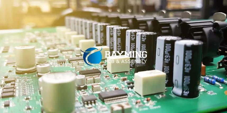
Whether you are new to the PCB industry or are looking to improve your PCB manufacturing process, there are certain factors you should consider. These include surface-mount technology vs. through-hole technology, the dielectric constant, and loss tangent. These factors can significantly impact the production of commercial PCB assembly services.

Surface-mount technology vs. through-hole technology

A better understanding of surface mount technology vs. through-hole technology will help you optimize your PCB assembly capabilities. Instead, the process involves applying solder paste to a PCB stencil and placing components on the surface.

Although surface mount technology has several advantages, it can also have disadvantages. One disadvantage is that surface mount components are not as large as their through-hole counterparts. In addition, the process of mounting components is also time-consuming and requires more advanced equipment.

Through-hole technology helps to mount electronic components, but it can limit routing space on multilayer PCBs. Despite this disadvantage, it has been helpful for years in electronics manufacturing. It is also helpful for some products, such as connectors, which require strong mechanical bonds.

Although it is not as efficient as surface mount technology, it is still more efficient in certain situations. It is the best type of board assembly for high-volume productions. It can also be essential for prototypes and small-scale projects.

Composition

Through-hole components are made of metal and contain leads that go through drilled holes in the board. We solder the lead wires to a solder joint on the other side of the board. However, these leads take up much more space than surface-mount components.

Efficiency

Surface-mount components do not need drilled holes, which results in smaller and more efficient PCB assemblies. These components are also more compact, and we can apply them to both sides of a board. In addition, they have small lead diameters, which increases the amount of component density.

Speed

Surface-mount technology is also faster than through-hole technology. As a result, assembling components is faster, resulting in lower production costs. It also allows for the use of a higher pin count. Although each type of PCB assembly solutions has several advantages and disadvantages, the mixed assembly is considered the better choice.

Application

Surface-mount technology is more widely helpful in the electronics industry than through-hole technology. It is easier to mount electronic components and can save time and money.

Loss tangent

FULL PCB MANUFACTURING Quote

Besides the requisite copper and epoxy layers, a handful of other factors go into making a commercial custom circuit board. A savvy manufacturer knows that choosing the right material for the job requires carefully selecting the appropriate components and a bit of forethought on PCB assembly requirements. The dielectric insulator is no exception.

The best way to go about it is by choosing a material rated for a particular application based on cost, functionality, and performance. The result is an aesthetically pleasing product that translates to increased productivity and a reduction in overall cycle times. Of course, with the advent of the internet, there are many options for choosing the best component suppliers, but the adage is still true.

Shopping around for the best rates and service is a good idea. An excellent place to start is with your local distributor’s literature or online product catalog. In addition, a knowledgeable sales representative can be a valuable asset to your company’s bottom line.

A good design guide will also help select the right component for the job. One thing to remember is that a high-quality component will require the proper tooling and some elbow grease. This is a particularly critical consideration for high-frequency applications. An excellent place to start is with the most common materials in the PCB market, such as lead-free solder, nickel, and aluminum. Besides the common materials, we can engineer many advanced materials, such as dielectric composites and glass-filled materials, to produce designer dielectrics.

Dielectric constant

Printed circuit boards are the building blocks of industrial and consumer electronics. They consist of a non-conductive substrate layer between copper layers. Various materials help in PCB assemblies, which have numerous desirable properties. Among these properties, one of the most important is the dielectric constant.

This property is essential in high-frequency applications. If the dielectric constant is high, the signal propagation speed will be slower. Therefore, it is preferable to use a material with a stable dielectric constant for safe and effective operation.

Generally, a PCB’s dielectric constant depends on its embedded system’s frequency and the material’s properties. A dielectric material suitable for a high-frequency application must have high thermal and electrical conductivity and chemical resistance.

Material

For high-frequency applications, the best material to use is polyimide. It has excellent chemical and thermal properties and is flexible at high temperatures. However, it is expensive.

Polytetrafluoroethylene (PTFE) is another popular material for high-frequency boards. It is a synthetic polymer. PTFE has excellent properties for high-frequency circuit boards, but it is expensive. It is also challenging to etch in ferric chloride. It has a low dielectric loss and dissipation factor.

Another material to consider is polyethylene, which has excellent physical and electrical properties. However, it is mechanically soft and has poor solvent resistance. It is also challenging to clad.

Polyester is also a good material for high-frequency applications but is not ideal for microwave devices. It has a dielectric constant of 3.5 to 4.0 and a dissipation factor of 0.004 to 0.014 at megacycles. It is a good choice for high-speed circuit boards.

A third material, polyphenylene oxide, has a dielectric constant of 2.55. It is also challenging to etch in ferric chloride. In addition, it has a dissipation factor of 0.0009. It is also expensive and challenging to laminate. Nevertheless, it is usually helpful in single-sided consumer electronics. Its electrical properties are similar to those of Teflon fiberglass.

FR-4 is the most widely used material in PCB assemblies. It is an epoxy-compound material woven from glass fibers. It is considered the universal standard for PCBs.
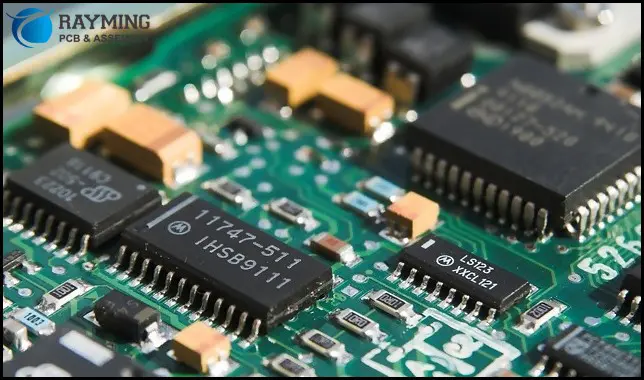
PCB design

Several factors influence the cost of PCB assembly services. Among these are the type of components used, the materials used, and PCB assembly services.

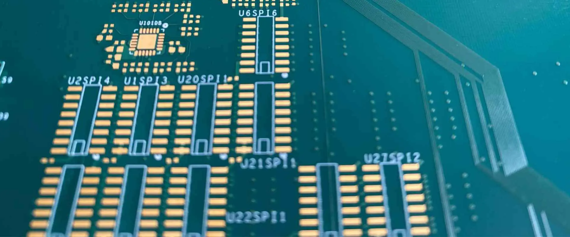
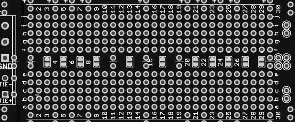
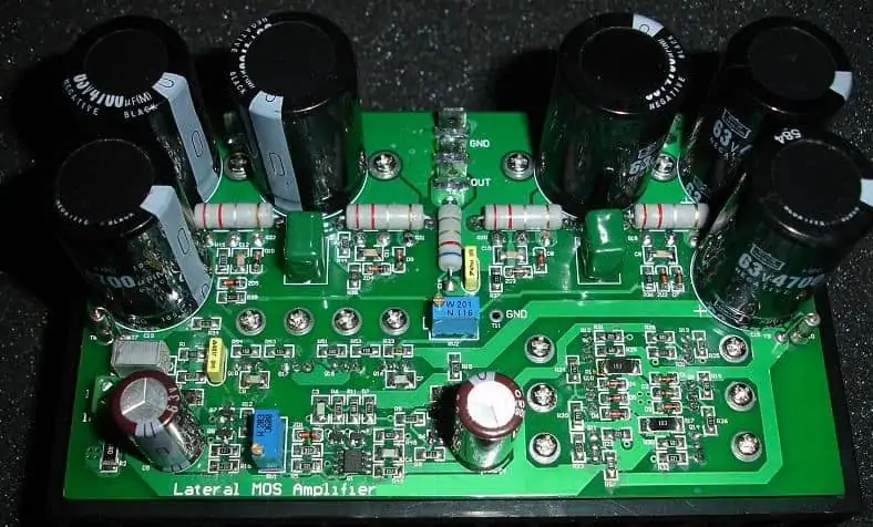
An essential component of any PCB is the copper traces. Copper traces are necessary to establish connections between components. We form Copper traces by cutting copper from a solid metal sheet.

Another essential element of a PCB is the vias. Vias are conductive, copper-colored bands insulated from the board substrate material. The shape and location of traces affect the layout of a PCB. Vias can be single or multiple layers.

We should consider traces early in the design process. Traces that are too close together can cause problems with crosstalk. Too wide traces can increase the number of layers needed and the printed circuit board assembly size. Traces that are too thin can also cause problems.

We should place traces at right angles to avoid capacitance problems. This is especially true for high-speed signals. Traces that are too close together can result in shorts. Traces should also be in a way that reduces the risk of crosstalk.

Multilayer PCBs are also becoming more common. This design type allows for more routing options. They also can help to decrease printed circuit board length and increase component density. The design also allows for the separation of power and ground planes. This helps to manage power efficiently.

Cost

Another important factor influencing the cost of a commercial custom circuit board is the number of layers. Multilayer PCBs can also help to reduce EMI and improve signal frequencies.

Size

Other important factors influencing the cost of a commercial custom PCB are the size of the board, the type of components used, and the number of parts. In addition, component type and technology can influence the cost of a PCB.

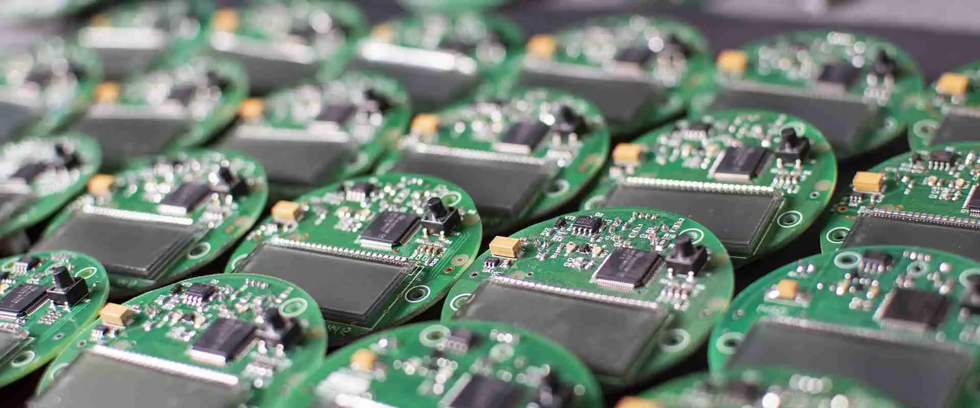
PCB Manufacturing process

Lastly, the type of PCB board fabrication process is essential. For example, semi-additive processing is commonly helpful for multilayer printed circuit boards. This process is a good choice for components that are small in size because it allows for maximum component packing density.

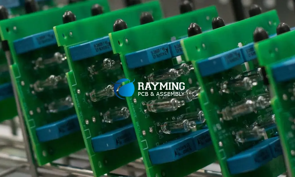
Why Choose Prototype and Quickturn custom PCB assembly services

SMD Components

Choosing a PCB prototype and Quickturn PCB Assembly service can help reduce your costs while ensuring your product goes to market quickly. These services will also help you identify design and manufacturing problems before a full-production run. If you decide to hire a service provider, make sure that you choose a company that can deliver high-quality printed circuit boards in the shortest time possible. You should also ask about certifications and quality control.

Technology

Prototype PCB Assembly consists of state-of-the-art technology and materials. They are fireproof, waterproof, and anti-static. They are ideal for testing individual components and the function of a complete PCB design. This helps you catch design flaws, errors, and inefficiencies early in the PCB manufacturing process. Using a prototype can also reduce the time and money spent on redesigns and rework.

Affordability

Prototypes are also more affordable than standard production PCB assembly. The price of PCBs varies according to the PCB design, materials used, and production techniques. Also, the PCB’s packaging type can affect the final cost. For example, some printed circuit boards require double-sided plating, and other PCBs can have single or multiple layers. Different PCB assembly requirements vary with surface finishes. Some designs may need a model to illustrate how the product works. A visual model can also be used to check for visual mistakes.

Compatibility

Quick-turn PCB assembly services are perfect for a range of different PCB designs. These services provide quick turnaround time and high-quality circuit boards. They can deliver them within 48 to 72 hours, which is perfect for urgent projects. However, other quick-turn PCB assembly services on the market aren’t as reliable. So make sure to choose a PCB manufacturer that can deliver high-quality circuit boards in the fastest time possible. You should also ask about certifications, quality control, and certification processes.

Quality of commercial PCB assembly services

Getting a product to market is essential for generating revenue and staying ahead of the competition. However, having a design that has design problems can cost you a fortune. This is why choosing a PCB manufacturer that can provide high-quality prototypes and Quickturn PCB Assembly services is essential. This will help you to ensure that your project is successful.

Reduce errors

Prototypes are used throughout the design process, as they help to eliminate guesswork and help engineers and technicians test the functionality of a product. This allows them to catch errors early on and prevent costly rework later in production. Prototypes also enable quick variations of a design before a full production run. These changes can be costly and time-consuming, so having a prototype allows you to test multiple designs before making a final decision.

In addition to using prototypes to test the functionality of a product, manufacturers can also use them to identify defects and inefficiencies in their design. Prototypes can also be ideal for testing individual components and troubleshooting. They can also help to show a client how their product works, which reduces time spent explaining to customers how to use it.

MCP9808T-E/MS: A Digital Temperature Sensor for Consumer Electronics

MCP9808T-E MS

Have you ever passed by a car and its horn started blaring? It can be scary and you may have wondered why that happened. More often than not, the carโ€™s horn blares when it โ€œsensesโ€ that someone or an object is coming closer to it. The same scenario plays out when a vehicle is in motion and depending on the customization, it swerves a little to avoid a collision.

All those and many other examples go to prove how sensitive consumer electronics have become. Sensors are now a part and parcel of these products and you have to take note of how each of these sensors work. The temperature sensor is one of the most outstanding but that doesnโ€™t mean that there are no other options out there. We also have variants like the:

  • Position sensors
  • Force sensors
  • Strain gauges
  • Pressure sensors
  • Motion sensors
  • Radio Frequency (RF) sensors
  • Optical sensors
  • Ultrasonic sensors

What is a Temperature Sensor?

FULL PCB MANUFACTURING Quote

Generally, it is a type of sensor that โ€œsensesโ€ or takes note of the change in a consumer electronicsโ€™ device. However, there are more meaning to that and we will break those down.

A temperature sensor is a dedicated sensor that detects and measures the amount of coldness and heat that is generated in a consumer electronics. The idea of detecting these is to correlate the outcome to the predefined values to ensure that the current temperature is not below or above those values.

Once the detection is made, the temperature sensor typically releases the value in the form of a digital or analog output.

In addition, the digital temperature sensor is one of the most-used, because of the simplicity. According to Analog Devices Incorporated, a digital temperature sensor like MCP9808T-E/MS tends to have a feasible interface, which could be either the I2C interface or the Serial Peripheral Interface (SPI).

MCP9808T-E/MSโ€™s Maximum Accuracy

If there is one feature to look for in a digital temperature sensor, it has to be the accuracy of the signal. MCP9808T-E/MSโ€™s accuracy is maximum and can be typically projected up to ยฑ0.5หšC.

Although temperature sensors are noted for the limited range, that of MCP9808T-E/MS can go a long way to transmit the converted signals in good time. As per the information in the datasheet, it can convert temperatures between -20หšC and +100หšC to a digital word of ยฑ0.5หšC.

MCP9808T-E/MS Supports Multiple Interfaces

It is better for a digital temperature sensor to work in unison with other supported peripherals and interfaces, as that could facilitate the speed of temperature sensor. Therefore, we are delighted to see that MCP9808T-E/MS supports multiple interfaces.

This support is rendered via the industry-standard, 400 kHz, 2-wire, SMBus/I2C-compatible serial interface. This interface standard allows the sensor to establish connections of up to sixteen (16) sensors โ€“ and all these would be controlled with the same serial bus.

MCP9808T-E/MS is User-Programmable

Given the many options in the market today, most consumers prefer going for the electronics and related products that can be easily fixed. In that regard, we are looking at electronics that are flexible enough for these users.

In the same light, MCP9808T-E/MS has been configured along those lines. It has a wide range of user-programmable registers, which provide the much-needed flexibility for temperature sensing and conversion.

Here are some of the techniques involved:

1. User-Selectable Settings

The users are allowed to program and reprogram the MCP9808T-E/MS digital temperature sensor as per the specifications of each application. The user-programmable settings include the specifications of the temperature critical output limits and the temperature alert window.

The users, or the digital circuit designer, can also program the power options/settings, such as the low-power and the shutdown modes.

2. User-Programmable Temperature Limits

The temperature at which the MCP9808T-E/MS functions or operates is also another programmable setting offered. Here, the users get to program the sensor with the critical temperature and the temperature window limits.

How this plays out is that the MCP9808T-E/MS gives out an alert signal anytime the temperature changes beyond or goes above the specified boundary limits.

When that happens, the users have the option to reprogram or reset these limits, especially the alert output signal polarity. It is up to the users to either set the polarity as an active-high or an active-low comparator output if it were to be used for the thermostatโ€™s operation.

Otherwise, it would be a great idea to reset the polarity to temperature alert interrupt inputย if it is for the microprocessor-based systems.

MCP9808T-E/MSโ€™s Pins

MCP9808T-E/MS supports up to five (5) pin configurations and each of those pins are optimized to work in a certain way.

Here are some of them:

  • Power Pin: Also known as the VDD pin, the power pin is the primary pin that powers the MCP9808T-E/MS digital temperature sensor. For accurate performance, it is to be connected in line with the operating voltage range specified in the DC.
  • Serial Data Line: It is also known as the SDA. The Serial Data Line is the pin configuration that serves as a bidirectional input and output pin. It works best with a pull-up resistor and is primarily used to make a serial transmission/transfer of data to and from the host controller.
  • Temperature Alert, Open-Drain Output: This is MCP9808T-E/MSโ€™s Alert pin. It works by giving out a signal (alert) when the predefined temperature value or ambient range of the MCP9808T-E/MS goes beyond the original value.
  • Serial Clock Line: Clock performance is also required for a digital temperature sensor to work accurately. MCP9808T-E/MSโ€™s clocking is regulated by the Serial Clock Line (SCL). Either of the master controller or the host controller located in the serial bus generate the clock. The Serial Clock Line (SCL)โ€™s primary function is to make the timing and communication of the digital temperature sensor to be relative to the signal in the pin/line.

Final Words

MCP9808T-E/MS doubles as a local and digital temperature sensor type with a local sensing temperature of 125หšC, maximum. It has a 10-b resolution, supports up to 5.5 volts of supply voltage and includes a wide range of features, including shutdown mode, output switch, programmable resolution and programmable limit.

XC9572XL-7VQG64Iโ€™s CPLD is Ideal for High-Performance Applications

Xilinx Spartan-7 FPGA

It is generally believed that Field Programmable Gate Arrays (FPGAs) are one of the embedded or Integrated Circuits (ICs) with a mix of complicated and flexible design processes. However, it is not entirely true. There are some other embedded devices, such as CPLDs that function the same way.

One factor to look for when choosing an embedded device or IC is the target application. More of than not, the ICs are designed for use with the applications or devices that have a higher-performance requirement. If that is what you are looking for but not in the form of an FPGA, we would be delighted to introduce you to a CPLD.

What is a CPLD?

The full name is Complex Programmable Logic Device. From that, you can guess that these types of devices are โ€œcomplexโ€ or a โ€œbit hard to configure.โ€

It is rightly so because a CPLD is first, optimized as a user-programmable device that can be leveraged to perform a wide range of complicated tasks, including information processing and several other logical operations.

The complexity of the CPLDโ€™s functionality stems from the support, integration or incorporation of a higher functionality, in the form of a set of logic gates. These gates are then used to facilitate the deviceโ€™s programmability.

Introducing XC9572XL-7VQG64I as a CPLD

FULL PCB MANUFACTURING Quote

There are several types of Complex Programmable Logic Devices (CPLDs), and from different manufacturers. XC9572XL-7VQG64I is a CPLD with support for a wide range of computing systems and pin counts.

In the subsequent paragraphs, you will find out more about this CPLDโ€™s functionalities and the components that make it worth the while.

The Target is for High-Performance Applications

When we say โ€œhigh-performance applications,โ€ reference is being made to the applications that require a higher functional capacity. Worthy of mentioning here is that XC9572XL-7VQG64Iโ€™s CPLD is optimized for low-voltage applications, particularly those used in computing systems and leading-edge communication markets.

Improved CPLD Functions with Xilinxโ€™s Innovative Product

A long time ago, the functionality of CPLDs was limited to the traditional process of analog sense amplifiers to boost the deviceโ€™s performances.

However, all that has changed with the innovative product or architecture introduced by Xilinx, the manufacturer of the XC9572XL-7VQG64I CPLD. The name of this architecture is CoolRunnerTM-II CPLDs.

The manufacturer released it to offer better programming and optimization optics for the CPLDs. At the core of the CoolRunnerTM-II CPLDsโ€™ functionality is the use of an โ€œinnovative all-digital core to achieve the same levels of performance at ultra-low power requirements.โ€

You will recall that we mentioned that the traditional design of a CPLD is to be used as an in-house programming platform for configurable devices. To that end, the CPLD typically involves the optimization of low-voltage applications that require higher performances.

However, the CoolRunnerTM-II CPLDs offer to deliver almost the same levels of performance (i.e., the high-performance and low-voltage requirements), irrespective of whether the optimization is to be done on only the ultra-low power applications.

Cross-Platform Design Support

Ordinarily, if we are to depend on the traditional format of optimizing CPLDs, we could have been looking at a one-sided model.

It is to the advantage of the new-generation configurable devices that the CoolRunnerTM-II CPLDs were released. With these types of CPLDs, it would now be possible to optimize the target applications across different facets.

For example, it allows for the use of the same CPLD architecture to configure both the low-power designs and the high-performance designs and in real-time.

The Generally-Combined Architecture

Even without the CoolRunnerTM-II CPLD, the XC9572XL-7VQG64I can function to a greater extent. According to Xilinx, the range of CPLDs it manufactures are optimized to comprise the following:

  • A bank of macrocells
  • The AND/OR array

On the one hand, the bank of macrocells are the โ€œfunctional blocksโ€ the perform either the sequential logic or combinational logic. These functional blocks are also designed to have or support added flexibility for either complement or true purposes. These blocks are usually laced along the varied feedback paths.

On the other hand, the AND/OR array is the second part of the traditional CPLD architecture. It works by performing a wide range of logic-centric functions.

Power Reduction Capabilities

XC9572XL-7VQG64I can conveniently cut down on the excessive power to be dissipated from the device. The power reduction capability is derived from the configuration of each of XC9572XL-7VQG64Iโ€™s macrocells to be used for the low-power mode.

While that is going against the default design of the CPLD for high-performance uses, it can help save power for the devices.

Besides, XC9572XL-7VQG64I can also cut down on excessive power usage by configuring the software to automatically delete the unused macrocells and product-terms.

XC9572XL-7VQG64I CPLDโ€™s System Reliance is Impressive

You can count on the excellence of the XC9572XL-7VQG64I CPLD, because of the quality it offers. Included here is the Electrostatic Discharge (ESD) of 2,000V, the endurance rating that exceeds 10,000 erase cycles and the 20-year data retention capabilities.

Routing and Connection Capabilities

XC9572XL-7VQG64I is able to maintain a higher and more-connected CPLD architecture because of the innovative connection capabilities.

Enabled here are the implementation of bus-hold circuitry on all the user pin inputs, the in-system programmability and the superior pin routing and pin-locking enabled via the Fast CONNECTTM II Switch Matrix.

Benefits of XC9572XL-7VQG64Iโ€™s CPLD

There are several reasons why you should choose XC9572XL-7VQG64I as your preferred Complex Programmable Logic Device (CPLD). These are some of the benefits of doing so:

1. It has a Scalable Architecture

If XC9572XL-7VQG64I were to rely on the traditional use of โ€œanalog sense amplifiers,โ€ it would likely take a lot of time before it scales the design process.

However, the replacement of these amplifiers with the CoolRunnerTM-II CPLDs is a good move in the right direction.

Among many other things, the CoolRunnerTM-II CPLDs allows for design scalability for both the high-performance and the low-power devices.

2. Feature Enhancements

The CoolRunnerTM-II CPLDs, being the main architecture that powers XC9572XL-7VQG64I, also opens up the devices for future, feature-rich enhancements. It also paves the way for the costs of manufacturing these devices to be minimal.

Conclusion

XC9572XL-7VQG64I is an innovative CPLD, powered by the CoolRunnerTM-II CPLDSโ€™ architecture. It supports dual-configuration for both low-power and high-performance devices; aggressive cost reduction and a scalable CPLD architecture.

How Surface Mount Technology impact PCB production from OEMs

Online PCB assembly quote

What Does SMT Line Stand For in printed circuit boards?

Essentially, an SMT line is a production line for manufacturing PCB boards. It is composed of various machines that process and place electronic components on the printed circuit board. The essential equipment includes a screen printing machine, a reflow oven, and a solder paste screen-printer.

SMT is essential for electronic circuits that require high performance and density. It is an efficient and cost-effective method for electronic circuitry production. It is also known for its high quality and reliability.

Surface mount technology is also known for its ability to reduce weight by approximately 60%. It also reduces electromagnetic interference. In addition, SMT is a faster process. This makes it an ideal choice for complicated circuits.

It is also considered an environmentally friendly process since it reduces using raw materials and electricity. We can also automate the process. It is, therefore, instrumental in many areas of life.

Surface mount technology is also known for its high-quality efficiency and low cost. It continues to evolve as new types of components are developed. Some of the latest developments are ultra-fine pitch SMD components.

The basic process components include screening, mounting, reflow soldering, and inspection. Each of these components has its role in the production process. For example, the screen printing machine is at the forefront of the SMT production line.

A reflow oven is behind the place machines. The process of reflow soldering involves mass heating preplaced solder paste. The heated solder then recedes, leaving irregularly shaped mounds of solder.

What Do SMD and SMT Stand For?

Earlier, two types of components soldered on the circuit boards: through-hole and surface mount components. Through-hole components are better for high-voltage parts. In contrast, surface mount components are smaller and more compact.

Through-hole mounting is also a better choice for significant, bulky components. Typically, we mechanically secure these parts before being soldered. However, we cannot package some surface mount components in standard sizes.

In the early years, hand soldering helps to attach these surface mount components. Then, small pieces of lead and silver connect the components. The process became more refined in the 1980s. As a result, it reduced the number of devices produced, improved performance, and made manufacturing more efficient.

The primary difference between SMT and SMD is the mounting process. With SMT, the components are fixed directly to the printed circuit board. As a result, SMT is much faster and easier to use and can also save space.

SMT is also a more cost-effective manufacturing process. It is more efficient because it reduces the number of people needed to produce the device. It also allows us to place more components closer, saving space.

While through-hole mounting is more efficient for large, bulky components, SMT can be helpful for smaller components. This method saves space and reduces by two capacitors.

When selecting the appropriate carrier tape, choosing one that protects the surface mount components and minimizes product loss is essential. A good cover tape will also ensure a smooth pick and place process.

EMS SMT in PCB Assembly

EMS stands for Electronic Manufacturing Services and is a service provided by a third party to a PCB supplier to facilitate the assembly process. This includes surface-mount strategies, solder component techniques, and turnkey PCB assembly.

Surface mount components

During the 1960s, scientists developed a new method of assembling PCBs. The technology allowed PCB manufacturers to build highly complex and packaging electronic circuits into smaller, more efficient printed circuit board assemblies. The process, referred to as surface mount technology, also reduced components’ required space.

Surface mount technology is a process in which components are mounted directly onto the PCB surface. The advantages of this technique include a higher degree of automation and repeatability, as well as good cost efficiency.

Two primary technologies allow manufacturers to mount components onto PCBs: surface mount technology (SMT) and through-hole technology (THM). However, even though the two methods are often helpful interchangeably, there are some significant differences.

Surface mount technology was initially ideal for higher speed and automated production, as well as small-scale assemblies. On the other hand, through-hole technology is a less common option due to its cumbersome design. However, the two technologies have been able to work together to provide reliable PCBs.

While both methods allow for a highly efficient PCB assembly, surface mounting has several advantages over through-hole technology. It reduces the amount of space required for components and allows for more flexibility in manufacturing. It also provides better moisture sensitivity, allowing the PCB to work reliably in the most demanding environments.

Despite the advantages, it’s important to remember that surface mount technology is not always the best choice for PCBs. Depending on the applications, a through-hole solution may be more appropriate. Also, we must take into account mechanical and electrical considerations.

SMT PCBs also require more manual debugging. While the process is simple enough, the actual identifying and debugging may be more challenging.

Solder component technique

FULL PCB MANUFACTURING Quote

Whether you are a PCB manufacturer or an individual, knowing the right solder component technique to use for your PCB assembly is essential. Choosing the right soldering technique can affect your costs, time to market, and revenue. However, choosing a technique that is right for your PCB’s requirements can be tricky.

Several soldering techniques are essential in PCB manufacturing, including soft, hard, and brazing. Each technique is helpful for different PCB components. For example, soft soldering is ideal for electronic components that have a small diameter. Hard soldering uses a solid solder to create stronger solder joints. Brazing uses thermal expansion to assemble electrical components. The process is often helpful for mass printed circuit board production.

Selective soldering is more precise than wave soldering. This process uses CAD data to position a laser to form a solder joint. It also provides more flexibility in the process. In addition, the laser ensures that the soldering joint is consistent and high-quality.

Choosing the right ball grid array component for your PCB assembly will depend on the types of parts that you will be placing on your board. For example, if you use metal components, you should choose low-temperature soldering. However, using composite parts, you might choose soft soldering.

A tin-lead alloy is ideal for the filler metal. This alloy provides a union between the metals through diffusion. It also helps to prevent corrosion. However, tin/lead solder has a lower melting point than lead-free solder. Therefore, choosing a lead-free solder can also help to avoid tin whiskers.

Solder paste

Choosing the right solder paste for your SMT process is vital. You must consider many factors, including viscosity, alloy composition, and temperature. It is also essential to consider how the paste will be applied and stored.

Using a stencil is a common way to apply solder paste. A stencil ensures that we deposit the right amount of paste. We should deposit the amount of paste depending on the distance between the solder joints on the printed circuit board. For example, a five-ball rule recommends that a minimum of five solder particles should span the smallest aperture.

It is also important to note that oxidation can affect the performance of solder paste. This can occur if we store the paste in an unrefrigerated environment. Also, it can be affected by the moisture content in the room.

The viscosity of the solder paste will also depend on the printing process. During printing, we control the viscosity by the printing method, temperature, and the paste area we deposit.

Turnkey printed circuit board assembly

Using turnkey PCB assembly services for your project can significantly improve production efficiency and decrease costs. It can also provide a way to save time and avoid any miscommunication with vendors. These services also provide you with a single point of contact for your project. This allows you to get everything you need for your project in one place.

A turnkey PCB assembly service includes designing your printed circuit board, sourcing components, and manufacturing. This can be a good option for prototypes and small quantities of PCBs. It will save you time and money while delivering professional-grade PCBs promptly.

A turnkey PCB assembly service provides you with a single point of contact. This can be beneficial when you have changes to your project or want to monitor the test program. Also, a single point of contact can prevent miscommunication and ensure you’re getting the best product possible. This can be particularly beneficial if you are operating in a strict country and need to double-check that your PCB manufacturer meets the regulations.

The other reason you might want to consider turnkey PCB assembly is to reduce the number of vendors you deal with. This can be a time-consuming process for small businesses. It can also lead to errors and miscommunication. In addition, dealing with multiple vendors can lead to ripple effects, such as delays and wasted time.

EMS companies have embraced non-traditional industries

EMS companies have expanded their business sectors by embracing non-traditional industries in printed circuit board assembly. These include medical, automotive, industrial, and consumer electronics.

These industries offer a wide range of services. For example, EMS industry can design and manufacture replacement parts and packaging electronic circuits for consumer products. They can also perform repair and warranty services. They can also perform functional tests on products. These tests may cover the product’s visual, performance, and safety aspects. If the final product passes all of these tests, it will be ready to use.

EMS companies can also provide software and firmware development. These services can help increase the productivity of the factory. They can also identify and eliminate defects in the circuitry. They can also recommend improvements to the final version.

EMS suppliers can also help reduce costs for components and manufacturing. They can also create a digital twin of the manufacturing process. This will help prevent unplanned changes from happening. The EMS companies can also generate reports based on the company’s goals.

In addition, they can help develop software that is specific to the company. EMS suppliers can also provide network services. EMS suppliers can also provide logistics and customer service. They can also manage logistics and provide total lifecycle repair for their clients.

EMS companies can also help reduce costs for their clients. They can also increase the speed of delivery. They can also increase the accuracy of their work. A supplier can also use digital manufacturing tools to produce the product faster. They can also provide programmable robotic arms to boost their productivity.

Quality assurance inspection

During the SMT process, you must perform quality assurance inspections to ensure that your products meet the required standards. In addition, these inspections can help you find problems that could degrade the quality of your products.

QA inspections are ideal for finding the source of problems and taking the appropriate steps to remedy them. To ensure the effectiveness of your inspections, other organizations should define clear objectives and metrics for success.

You should also use quality-related records to document your quality control findings. Keeping these records up-to-date will ensure that you have proof of the quality of your products.

Using the right equipment will help you find defects in your products. You can use various test equipment to assess the quality standards of your printed circuit board. X-RAY testing equipment is a popular option. It’s highly effective for BGA welding, as well as inspections of solder paste printing.

Using quality-related records can also help you detect problems in your products. Aside from the items mentioned earlier, you can use photos and videos to document quality control findings.

Cost

Several factors influence the cost of the SMT process. These factors include the quantity of electronic, the number of components, labor, and the type of technology.

SMT has become an essential part of the electronics manufacturing industry. It has improved the processing cost and speed of production. It has also made electronic circuitry design easier.

There are two major processes involved in SMT assembly. These processes include stencil printing and solder paste application. Unfortunately, these manufacturing processes are relatively complex. In addition, they involve the use of automated technologies. Therefore, the amount of manual procedures can also influence the cost of SMT assembly.

The quality of the product may also affect the cost of SMT assembly. Keeping the defects at an early stage may help to reduce the cost of prevention. Statistics show that preventing defects may reduce the cost by up to 5%.

Another factor affecting SMT assembly’s cost is the amount of unused inventory. Unused inventory occupies production space and does not add value. It also increases management costs. It can also limit the supply of through-hole components to the next process.

Using an Original Equipment Manufacturer for PCB Assembly

Using an Original Equipment Manufacturer (OEM) for your PCB assembly is a great way to save time and money. You’ll get an electronic built to IPC standards, and the attention to detail is top-notch.

OEMs can save money and time

Printed circuit boards are a crucial component of almost all electronic assembly. Although it may seem like an unnecessarily complex system, Original Equipment Manufacturer can do a few things to save time and money while getting the best quality PCBs.

An assembly service is a great way to relieve the pressure of coordinating multiple services. It also ensures you get a top-notch printed circuit board. In addition, you get the benefit of working with a skilled and experienced quick-turn PCB manufacturer.

A turnkey assembly service is the best way to ensure that your electronic is on par with the competition. It also reduces the risk of errors by allowing the designer to focus on the more technical aspects of the design. This includes designing the circuit board and certifying it to meet regulatory requirements.

The PCB assembly process is highly automated, which reduces the need for human labor and the corresponding errors. In addition, it allows for the use of standard through-hole components, which saves on material costs. In addition, it allows for the most efficient layout of the circuit board, which means more efficient production.

The PCB assemblies processes have evolved from highly manual and labor-intensive to automated and efficient. These advancements have made it possible for an Original Equipment Manufacturer to meet the demands of the modern consumer while staying competitive.

They follow IPC standards for PCB design

Whether designing or manufacturing a PCB, you should follow IPC standards. These standards are accepted worldwide. The program manager helps you to produce reliable PCBs that are durable and offer high performance. The benefits of IPC standards include minimizing manufacturing errors, ensuring a smooth workflow, and increasing brand recognition.

The Institute for Printed Circuits (IPC) is a trade association that designs and publishes system standards for PCBs. IPC members include board manufacturers, manufacturers, designers, and suppliers. IPC has more than 3,000 members from different segments of the electronics industry. The organization has offices in China, India, and Sweden. It offers training, research, and public policy lobbying.

PCBs have become essential in many industrial sectors. The reliability and performance of these products are necessary to maintain market competitiveness. OEMs know PCBs’ importance and prefer to work with PCB manufacturing service providers.

The IPC standards for PCB design include specifications for wire harness assemblies, harness assembly, electronic enclosures, PCB assemblies, and solder splices. In addition, they address reflow soldering, wave soldering, and other electrical work on PCBs.

The PCB design standards also include the classification of PCBs into three general classes. Class 1 products, Class 2 products, and Class 3 PCBs. They place stricter cleanliness requirements on electronic assemblies.

How to Avoid Electrostatic Discharge on EMS Systems

Whether you have an electronic design or are an electronic manufacturing company, there are a few steps you can take to ensure you avoid electrostatic discharge. These steps include designing a electronic with an “ESD Secured Area” and implementing preventive measures.

Precautionary measures

Printed circuit boards (PCBs) can spoil from electrostatic discharge. The main factor in determining ESD risk is the electromotive force that causes current flow.

To minimize ESD risk, you must design a properly grounded electronic. In addition to grounding, you should also run a broad ground track around the edge of the electronic.

To prevent ESD from damaging your PCBs, you should use a transient voltage suppressor (TVS) at your devices’ input and output ports. You can also use surge protection diodes to reduce the potential for an ESD incident.

Catastrophic failure is the least costly type of ESD damage

Keeping your electronic devices and equipment safe from ESD damage is more critical than ever. Although it’s hard to prevent ESD damage completely, there are measures you can take to mitigate the risk. These measures range from simply wearing ESD wrist straps to installing a grounded workstation.

There are three main types of ESD events that could damage your device. Each type of event has unique benefits, but we can achieve the best protection by understanding the difference between them.

The simplest form of ESD is triboelectric charging, which is a process that allows electrons in a material to lose electrons. The best ESD protection is to design your products with equal voltage levels so that the charge does not affect the voltage.

A more complex process is electrostatic discharge, which is a surprisingly common occurrence. An electrostatic discharge is a sudden discharge of electric current.

Identify and define an “ESD Secured Area” on the PCB

Identifying and defining an “ESD Secured” area is the first step in avoiding electrostatic discharge (ESD) in your manufacturing facility. The best way to approach this is by defining a demarcated area for ESD-sensitive systems. To prevent ESD-related failures, ensure that all machines are packaged in a manner to avoid electrostatic damage. To make this a reality, use an ESD protection diode as part of the ESD shielding solution. If this is not an option, use a transient voltage suppressor to prevent ESD-related failures. The best way to do this is to use a non-conductive adhesive.

Simulation of EMS PCB systems

Using the EMS system to simulate Electrostatic Discharge (EMI) and Electromagnetic Compatibility (EMC) is an essential part of the design process for PCBs. EMC standards define the permissible limits for radiated and conducted emissions in commercial and industrial systems. These standards also require that devices do not impede other systems.

An EMS system can simulate a wide range of electrical machines and devices. These include valves, actuators, loudspeakers, high-voltage apparatus, bus bars, and more. In addition, the system interface allows a user to select the testing criteria needed to determine compliance.

EMI/EMC impacts a wide range of systems, including the International Electrotechnical Commission (IEC), the Center for Devices and Radiological Health (CDHR), the Federal Communications Commission (FCC), and the International Standards Organization (ISO).

Additive Manufacturing Vs. Traditional PCB Design and Layout

Shengyi Autolad1 PCB

Traditional PCB Manufacturing Methods

Printed circuit boards (PCBs) are helpful in various electronic products. They consist of electric conductors, insulating layers, and solder masks. They are used to create electronic circuits and eliminate the need for connecting wires and breadboards. PCBs are also used to reduce the size of a device.

PCBs consist of copper and fiberglass. These materials are stable, water-resistant, and have good optical properties. However, other materials are used from time to time.

We design PCBs using CAD software. This allows designers to visualize a computer aided design on a 3D board and to use different substances. In addition, some PCB manufacturers are now using 3D printers to create customized PCBs.

The first step in manufacturing a PCB is to design a PCB board. This involves designing the board‘s layout, drawing sketches, and 3D printing schematics. Then, using PCB design software, designers can layout the electronics and run simulations. Finally, we encode the design in a Gerber file, which then incorporates into the PCB’s schematic.

Differences

Whether designing a PCB for manufacturing or simply for design and layout purposes, you will likely have heard of both additive manufacturing and traditional PCB manufacturing methods. The main difference between these processes is how we make the board. Whether by additive manufacturing or traditional manufacturing techniques, the finished board is a thin layer of conductive metal or plastic layered over substrate materials. In electronics manufacturing, they produce the entire board by creating the material by mixing and extruding liquids into the air. In traditional PCB design and layout, the material is added to the electronics by laying down layers of copper or other metals one at a time. This additive process is called plating.

PCB plating process

Plating the PCB is a process that protects the copper from corrosion. It also forms a conductive carbon layer that enhances the surface finish of the PCB. There are several different plating processes available. Understanding the various options available can help you make an informed decision about your PCB.

The PCB market has evolved to include electrical components plated with copper, form factor, gold, and nickel. In addition, the market also includes electrical components plated with tin.

There are several different PCB plating processes, including semi-additive, additive, and subtractive. The PCB plating process is an essential step of electronics fabrication, and fabricators must ensure the process is reliable.

Additive processes use less material and generate less waste. Typical PCB plating thickness values range from 10 micro-inches to 100 micro-inches. In addition, some processes allow you to test every layer during the fabrication process.

Inkjet printing vs. laser cutting machines

Compared to laser cutting machines, 3D printing offers a few advantages. It is faster, more efficient, and less expensive. It also provides a safer alternative to laser marking. In addition, it can produce a higher-quality stencil that can be helpful for various additive processes.

PCB manufacturing is a competitive industry. As a result, manufacturers are seeking to reduce costs and increase productivity. We can achieve this by reducing the number of steps in the manufacturing process. The PCB industry is also moving toward automation and producing more efficient products.

One technology that may help improve this is additive manufacturing. This additive process can create a new part layer by layer, similar to how a 3D printer would produce a piece of plastic. The process can create intricate designs and objects. It is ideal for creating 3D printing objects from metals and other substances.

PCB design for manufacturing

Unlike the old method of building a PCB, the additive manufacturing method allows for a wider variety of substances. This means more opportunities for manufacturers to experiment with new designs. There are more advanced materials for commercial 3D printers than just a few years ago.

For PCB designers, this means the freedom to build complex interconnect architectures. This also allows for a greater variety of finer traces and layers. The process is also cost-effective. This method also allows for a more complex PCB with less components.

The process is also a green one. Additive manufacturing uses CAD software and 3D object scanners. This new technology deposits material in precise geometric shapes.

The process can reduce tooling time, material waste, and industrial production costs. This is particularly important in the electronics industry, where there is a growing demand for multilayer PCBs.

Micro PCBs

Unlike traditional PCB design and layout, micro PCBs rely on the proper use of technology to ensure excellent functionality.

For starters, a micro PCB is usually two layers deep. This allows for closer component placement. However, it also adds several challenges to the manufacture of these boards.

One key challenge in designing and producing these boards is the smaller pitch. This means that the pin centers of SMDs will be closer together. This will decrease the overall pitch and reduce the package size. In addition, this will increase the overall reliability of the board.

The PCB also requires a backplane, a supporting plane that will help insulate the electronics. For this, we use a fiberglass substrate. This helps prevent breakage and provides core strength to the PCB.

How Does Additive PCB Manufacturing Work?

FULL PCB MANUFACTURING Quote

Depending on your PCB manufacturing method, you can get your PCB printed in various ways. This includes using Inkjet, Powder bed fusion, and SLS.

Inkjet style printing

Currently, this printing is an effective method for producing functional substances. Its versatility allows for fabrication a wide variety of products, from electrical devices to sensors to mechanical products. It is also compatible with conductive and dielectric inks.

3D printing is a non-contact deposition process that we can apply to many substances and substrates. It produces features down to 20 microns in high resolution. 3D printing is also an effective technology for fabrication solution-based functional substances. In addition to its versatility, it is also unique in its ability to produce fully functional products.

High-speed extrusion printers

Having a high-speed extrusion printer is essential for PCB additive manufacturing. These printers can print parts five to 15 times faster than the competition. In addition, having a direct drive extruder gives the user better control of the filament path. This provides better print quality.

Adding a liquid-cooled stepper motor to a commercial printer may also be beneficial. This type of printer can print at speeds up to 1 m/s. In addition, this type of mechanism decreases the risk of unsynchronization.

In addition to a direct drive extruder, the printer used a belt drive mechanism for the lead screws. This ensured a consistent operation. The printer also uses a liquid-cooled direct drive extruder for higher-quality prints.

FDM

During the last ten years, PCB prototyping has shifted from clay models to additive and subtractive manufacturing technologies. As a result, we can now produce PCB prototypes in a fraction of the time it would take to produce one through conventional methods.

In addition to being more efficient than conventional fabrication, PCB prototypes can also accelerate the development cycle for new products. A 3D-printed board model can help the PCB layout process and show how the parts connect. It can also limit the number of changes to the electronics.

One major drawback of FDM printed components is high surface roughness. This is due to the stair-stepping effect of the 3D printer.

Powder bed fusion

Unlike conventional 3D printing, powder bed fusion is an additive PCB manufacturing process that uses heat to fuse powdered material into a solid part. As a result, powder bed fusion has emerged as a viable method for mass fabrication polymers.

The process can create parts from metals, plastic, and other electronics. In addition, the parts can be helpful for prototyping and large scale production. In the commercial realm, powder bed fusion has been essential to creating parts for aerospace, defense, and other industries.

Powder bed fusion is a relatively expensive process. However, its advantages include the ability to produce parts that can be mass-produced and the ability to print parts that can be helpful in prototyping. These advantages make powder bed fusion a viable additive PCB manufacturing method for manufacturers.

There are several different powder bed fusion processes. Each process follows a similar set of steps to produce a final part. However, the processes also depend on a variety of variables. These variables can affect the overall quality of the part.

SLS

Unlike other 3D printing methods, SLS (Self-Limiting System) uses a precise laser to melt the powder into a single layer. This allows for the industrial production of complex parts without the constraints of traditional subtractive fabrication methods.

SLS is widely helpful in the aerospace, medical, and rapid prototyping industries. However, the lack of widespread availability of SLS printers remains a challenge.

Aside from the low cost, SLS is also considered a fast technique. This is because we can produce parts at low volumes without the constraints of traditional subtractive manufacturing methods. It is also ideal for self-supporting prototypes. However, SLS can also produce parts prone to inaccuracies and deformation.

Advantages of PCB Additive Manufacturing process

Solderable Breadboard

Using an additive manufacturing process for in-house PCB fabrication can help companies take control of quality and costs. It also frees engineers from the constraints of traditional manufacturing processes. In addition, the process allows companies to create more complex electronic devices, such as hybrid electronics and circuits for robotics.

Efficiency

One of the main benefits of using an additive manufacturing process for in-house PCB fabrication is reduced material consumption. The process uses various substances to melt the material, including lasers, print heads, and beams. The result is a product up to fifteen times thinner than traditional techniques. This reduces waste and overall industrial production costs.

In addition, additive PCB manufacturing can also be helpful for rapid prototyping. It is ideal for creating various parts, from rigid-flex electronic components to custom interior features. This technique allows engineers to prototype mechanical assemblies rapidly. It is also a great way to experiment with updated designs.

Cost

With a variety of substances available, the additive process is cost-competitive. While specialized components may cost more, they are usually less expensive than other methods. It is also a great way to reduce inventory waste. It allows companies to produce small batch orders and switch between products as needed.

Companies can take advantage of several other benefits with a full-scale in-house PCB fabrication system. This is especially important for complex devices. The process is also eco-friendly, not using toxic solvents or chemicals. It also produces fewer unsold products.

Speed

Another advantage of using an additive manufacturing process for in-house PCB fabrication is the speed. The process takes about three hours to complete a shape. This is faster than the traditional PCB manufacturing process, which can take up to an hour to produce a shape.

The process also eliminates the need for tooling. Tooling increases industrial production costs and delays the time it takes to produce a product. Additionally, tooling can cause various problems, such as operator exposure to toxic substances. Also, tooling can cause the creation of more components than necessary. These issues can lead to costly setups and inventory waste.

Security and cycle time

Other advantages of using an additive manufacturing process for in-house printed circuit board fabrication include security and cycle time. In addition, manufacturers can take greater control over product quality and intellectual property protection. This is especially beneficial for companies that operate in highly regulated industries. In addition, electronics fabrication allows companies to produce parts that are difficult to find. Bringing these manufacturing capabilities in-house can accelerate the R&D process.

Pollution

Finally, using an additive PCB manufacturing process for in-house fabrication frees companies from traditional manufacturing processes’ cost and time constraints. The process is also environmentally friendly and pollution-free. It also allows companies to use only the substances needed for a consistent finish. This helps eliminate waste and redundant steps.

As additive manufacturing technology continues to develop, it will change how we produce products. It will also create a wider array of fabrication options for manufacturers. In the future, it may even allow circuits to integrate into . This could revolutionize life-saving devices such as pre-surgical tools.

Application of Additive Manufacturing

Originally used in the aerospace industry, Additive PCB Manufacturing has expanded to various end markets. Its applications range from producing small parts for less volume applications to creating sophisticated products with advanced features.

Additive manufacturing uses nano dimension digital data to create a physical device. The process is helpful for rapid prototyping and fabricating complex non planar geometry
. CAD software can help describe the physical object, and a special 3D printer helps to create the part.

The ability to produce parts in small, low-volume quantities is a key benefit of additive manufacturing. It also reduces cost and the amount of material used in assembly. These benefits are especially beneficial in the mobility industry.

Additive Manufacturing is also more sustainable. It uses components that are more flexible and strong. As a result, it reduces the amount of material used in electronics manufacturing and decreases the amount of waste created during the fabrication process. These substances include metals, polymers, and filaments.

Additive manufacturing also enables designers to create complex geometries. The ability to manufacture complex assemblies makes additive PCB manufacturing a powerful tool for the automotive industry. The automotive industry can use this technology to manufacture PCBs with improved mechanical properties and enhanced comfort characteristics.

Additive manufacturing is also helpful in the medical industry, enabling companies to produce small parts in low volume. This is a benefit of the process for the aerospace industry as well. The aerospace industry uses parts that are lightweight and strong.

Developing printed circuit boards for Industrial Additive Manufacturing

Developing PCBs for Industrial Additive Manufacturing (AM) can effectively address many of the challenges associated with fabricating electronics. With the advent of additive manufacturing processes, designers have access to more flexible, creative, and faster printed circuit board prototyping.

AM provides a lower cost and faster lead time than conventional PCB prototyping. This reduces the risk of human error and delays in final product development. In addition, it allows designers to experiment with more complex board geometry.

Additive manufacturing is a process that uses CAD software and 3D object scanners to deposit substances in complex shapes. These substances build up level by level.

The process eliminates the need for subtractive etching and chemicals. Instead, printed electronics run at a lower temperature (150oC) and do not use toxic etchants. This helps reduce overall waste and material consumption.

With additive manufacturing, companies can produce a wide range of substances, including copper-based solderable circuits. These circuits are flexible and compatible with conventional reflow processes. They also cut costs and meet higher environmental standards.

The lead time for developing PCBs for Industrial Additive Manufacturing depends on the complexity of the product and material weight. As a result, companies may need to work with a traditional PCB manufacturing partner to produce smaller 3D printing jobs. But the advantages of AM may outweigh the additional design work.

AM is ideal for a company that wants to test a new design before going into production or for companies that want to experiment with new products. We can do this by purchasing evaluation boards for particular substances.

The Complete Guide to Audio Electronics and How They Impact PCB Design

Audio Electronics

The field of electronics is among the most dynamic today. Electronics are of different kinds, for example, aviation electronics, automotive electronics, audio electronics, etc. However, we will look at audio electronics in this article. Audio electronics are essential to music, from recording studios to live event venues. We couldn’t listen to the music we love without audio electronics. Nowadays, music is among the most paying industries in the world. However, we would stagnate without aviation electronics at some point, probably applying traditional music equipment that did not employ power. The following details will equip us with a deep understanding of audio electronics.

A Brief History of Audio Electronics

The first commercial audio system was in 1901, after the development of early audio electronics in the late 1800s. It was the first time music could be amplified and broadcast to a broad audience using a system that amplified sound using vacuum tubes.

The first public address system to set up was in 1922, and in 1920, the world achieved its first commercial radio broadcast. In 1925, the first home stereo system worked, and later in 1930, the first portable radio.

In 1947, the invention of the first transistor happened. Later in 1958, the world created the first integrated circuit. In 1979, engineers designed the first digital audio system. Later in 1997, the first portable digital audio player worked.

What are Audio Electronics?

Audio Electronics hardware

Audio electronics are electronic equipment that aid in sound processing and amplification. In addition, these include amplifiers, mixers, Equalizers (EQ), and sound processors. There are numerous applications for audio electronics, including live sound reinforcement, recording studios, and home audio systems.

Audio amplifiers help to increase the signal’s amplitude and volume. On the other hand, mixers mix several signals, whereas equalizers modify a signal’s frequency response. We can alter signal properties such as delay, reverb, and pitch with sound processors.

Audio electronics are integral to any sound system and can significantly impact sound quality. Therefore, when selecting audio electronics, it is essential to evaluate the specific requirements of the system and the desired sound quality.

Categories of Audio Electronics

We can broadly categorize audio electronics into two groups:

  1.  Active audio electronics: These require power from a source of electricity, such as a battery or the mains.

The amplifier is the most prevalent kind of active audio electronics. It raises a low-level signal to a volume appropriate for driving loudspeakers. Many amplifiers are available, including field-effect transistors, bipolar transistors, or vacuum tubes (valves) (FETs).

  • Passive audio electronics: These rely on the electrical characteristics of the parts themselves to operate.

Crossovers and equalizers are examples of passive audio electronics. Equalizers amplify or reduce specific frequencies to enhance the overall sound quality. Conversely, Crossovers divide an audio signal into various frequency ranges and send each range to a different loudspeaker.

Classification of Audio Electronics

There are three broad classifications for audio-electronic devices:

Audio Input Devices

The purpose of audio input devices is to convert sound to electrical signals. Microphones are the most frequent audio input devices. Microphones transform sound waves into electrical signals that audio electronics equipment may process. Line-level sources, such as CD players and tape decks, and digital audio sources, such as computers and MP3 players, are additional audio input devices.

Audio Processing Devices

Audio processing devices modify or improve audio signals. Amplifiers and equalizers are the most common audio processing devices. Equalizers adjust the frequency response of audio signals, whereas amplifiers enhance the volume of audio signals. Other audio processing devices include noise reduction and echo cancellation devices, which reduce background noise and echoes.

Audio Output Devices

These devices convert electrical signals into sound. In addition, the most common audio output devices are loudspeakers. Loudspeakers turn electrical signals into audible sound waves for listeners. Other audio output devices include headphones and earbuds, which help us to listen to audio signals privately without disturbing others.

Characteristics of The Audio Electronics Industry

FULL PCB MANUFACTURING Quote

The audio electronics industry comprises companies designing, developing, manufacturing, and selling electronic products for sound reproduction and recording. Amplifiers, microphones, mixers, receivers, speaker systems, and turntables are some of these items.

The audio electronics industry is a global market comprised of enterprises from North America, Europe, Asia, and other regions. The sector is highly competitive, with companies always seeking to develop new and improved items to fulfill consumer demands.

For the industry to remain competitive, continuous innovation is essential. The corporations must therefore make substantial investments in research and development to bring new items to market. Here are some of the numerous defining criteria that characterize the audio electronics sector:

The audio electronics sector is capital-intensive due to the complexity of audio electronics devices, which necessitates substantial investment for their development and manufacture.

Secondly, the audio electronics sector is economically sensitive since the demand for audio electronics frequently correlates with broader economic developments. For instance, consumers may be less likely to acquire expensive audio equipment during economic downturns.

Lastly, the audio electronics business has stringent regulations to guarantee that items meet safety and quality requirements.

The audio electronics business is an integral aspect of the worldwide economy. It plays a significant role in supplying customers with goods that allow them to enjoy music and other audio content.

Characteristics Of Audio Electronics

Frequency Response

The frequency response is the frequency range the system can reproduce. For example, the frequency response of most audio-electronic systems spans the audible range of 20 hertz to 20 kilohertz.

Signal-To-Noise Ratio

 The signal-to-noise ratio is the ratio of the audio signal level to the background noise level. A more excellent signal-to-noise ratio translates to a more audible and distinct audio signal.

Distortion

Distortion refers to any alteration to the waveform of an audio signal that was not part of the original signal.

Crosstalk

Crosstalk is when an audio signal leaks from one circuit to another.

Noise

Noise is any sound picked up by the undesirable system.

Applications of Audio Electronics

Audio Electronics PCB

Audio electronics are applicable in a variety of fields, such as:

Consumer electronics

Consumer electronics, such as televisions, DVD players, and digital cameras, are intended for daily use. In addition, audio electronics are an essential component of many consumer electronics gadgets for people to enjoy their preferred music, movies, and games.

Consumer electronics use various audio electronic parts, including speakers, amplifiers, and digital-to-analog converters. While speakers transform the electrical audio signal into sound waves that the user can hear, amplifiers boost the audio signal’s volume. It is easy to convert digital audio signals into analog signals so that amplifiers and speakers can process them with digital-to-analog converters.

In addition to being a sort of consumer electronics intended for wearing over the ears, audio electronics are also applicable in headphones. Using headphones with several gadgets, including MP3 players and cell phones, enables users to listen to audio without bothering others.

Medical Electronics

From cochlear implants and hearing aids to medical imaging and diagnostics, audio electronics are highly applicable in various medical applications.

The most well-known use of audio electronics in medicine is hearing aids. These gadgets boost sound waves so that the inner ear can pick them up, enhancing hearing for those with hearing loss. In addition, physicians stimulate the auditory nerve more directly with cochlear implants, comparable to hearing aids but for inserting into the ear.

Audio signals are applicable in medical imaging systems like MRI and ultrasound scanners to provide images of the inside of the body.

Audio signals are essential for diagnosis and monitoring, as in fetal heart and sleep, apnea monitors.

Medical research also makes use of audio electronics. To investigate illnesses like epilepsy and Alzheimer’s disease, for instance, audio electronics help to capture and analyze brain waves.

Telecommunication

In terms of the hardware components employed and the signal processing done on the audio stream, audio electronics are widely applicable in telecommunication.

Microphones, loudspeakers, headphones, earphones, and other transducers are examples of audio hardware components used in telecommunication. Microphones translate Sound waves into electrical impulses, which then undergo amplification and transmission to the loudspeakers. Loudspeakers convert the electrical impulses back into sound waves so that the person on the other end of the line may hear them.

For the person on the other end of the line to hear the audio signal more clearly, headphones and earphones help to separate the audio signal from the background noise. Echo cancellers, which eliminate echoes from the audio signal, and noise reduction systems, which eliminate background noise from the audio signal, are other hardware elements applicable in telecommunication.

Audio signal processing is essential in telecommunication to enhance the audio signal’s quality. Techniques for signal processing include equalization, noise reduction, and echo cancellation. For example, we can clean the audio signal of echoes using echo cancellation and eliminate background noise using noise reduction. Moreover, we can modify the frequency response of the audio signal can using equalization.

Telephone, cell phone, VoIP, and radio systems are examples of telecommunications systems that use audio electronics.

Automotive Electronics

Automotive electronics are the electronic components found in vehicles, such as the radio, car computers, ignition, and in-car entertainment systems. Applications for audio electronics in the car industry include infotainment systems, sound systems, and security systems.

Infotainment systems are in charge of providing entertainment and information to passengers while they are in the car. A radio, CD player, DVD player, and various connectivity options like Bluetooth and USB are perfect examples. A navigation system is a common addition to infotainment systems. Infotainment systems use audio technology to deliver high-quality sound reproduction.

The vehicle’s audio system might sound better due to improved sound systems. Examples are speakers, subwoofers, and amplifiers.

The usage of security systems helps prevent and identify crime. They frequently come with an immobilizer, an alarm, and a tracking system. In addition, security systems use audio electronics to provide an audible alarm.

Benefits of Audio electronics

Home Audio Electronics

The development of audio technology has enabled the recording and reproduction of sound with unparalleled fidelity. Wax cylinders and shellac discs recorded sound in the early days of audio recording. However, the sound quality could have been better, and the tapes could only go for a few minutes. Emile Berliner invented the phonograph, which used a celluloid disc to record and reproduce sound, in the late 19th century. Consequently, this enhanced sound quality and made longer recordings possible. In the 1930s, magnetic tape recorders made it feasible to record sound with higher fidelity. Digital audio technology has enabled the recording and reproduction of sound with near-perfect commitment.

Additionally, audio electronics have enabled the amplification of sound. In the early days of the music industry, tiny, intimate venues were typical. In the early 20th century, audio amplifiers made it possible to perform music in more extensive settings. From small clubs to enormous stadiums, audio amplifiers are an integral component of live music performances today.

Additionally, audio electronics have enabled the creation of special effects. In the early days of the music industry, mechanically modified musical instruments’ sounds produced extraordinary results. The arrival of electronic devices at the beginning of the 20th century enabled the creation of a vast array of new sounds. Today, audio electronics help us produce various special effects, including reverb and distortion.

Audio electronics have also enabled the creation of new musical genres. In the early days of the music industry, music was a yard of a handful of individuals. The emergence of audio recording and playback technology at the beginning of the 20th century made it possible for a single individual to compose music. Today, a wide range of individuals, from bedroom producers to professional musicians, make electronic music.

Which Are The PCB Types Employed In Audio Electronics?

PCBs are the foundation of audio electronics. Electronic components wouldn’t communicate with one another or work correctly without them. Single-sided, double-sided, and multilayer PCBs are the three most popular varieties used in audio electronics.

The most straightforward kind of PCB is single-sided PCB. They consist of a single layer of copper or another conductive material etched to produce the appropriate circuit layout. The cheapest and most straightforward to make are single-sided PCBs; however, there are restrictions on the types of components we can use and the intricacy of the circuits we can design.

Sandwiching two layers of conductive material, usually, copper, between two insulating layers forms double-sided PCBs. We then etch the desired circuit layout onto the two layers. Double-sided PCBs have the advantage of supporting more components and intricate circuits despite being more expensive and challenging to manufacture than single-sided PCBs.

Three or more layers of conductive material, usually copper, separated by insulating layers make up multilayer PCBs. Like double-sided PCBs, we etch the desired circuit layout into the layers. Although multilayer PCBs are the most expensive and challenging to produce, they can support the most significant number of components and the most intricate circuits.

Materials Suitable For Manufacturing Audio Electronics

The application of the audio device largely dictates the kinds of printed circuit boards (PCBs) used in audio electronics. For instance, a portable music player needs a different PCB than an audio power amplifier. These are the various PCB types used in audio electronics:

FR-4 PCBs

The FR-4 PCBs are the most popular kind used in audio electronics. FR-4 is a flame-resistant glass-reinforced epoxy laminate. Printed circuit boards, such as those found in power amplifiers that may work under high temperatures, often consist of FR-4.

Rogers RO4003

Rogers RO4003, a dielectric material, has a low dielectric constant and loss tangent. As a result, printed circuit boards that need minimal signal loss, such as those in portable music players, mostly require Rogers RO4003 technology to manufacture.

Polyimide PCB

Polyimide is a dielectric material with a high dielectric constant and loss tangent. Therefore, printed circuit boards with a high signal loss requirement, such as those found in power amplifiers, mainly consist of polyimide.

Teflon

Teflon PCBs consist of a fluoropolymer with a low dielectric constant and loss tangent. The teflon is frequently applicable in printed circuit boards with low signal loss, such as those used in portable music players.

Polycarbonate PCB

Polycarbonate is a thermoplastic with a high-loss tangent and dielectric constant. As a result, printed circuit boards that need a lot of signal loss, such as those in power amplifiers, are easy to construct using polycarbonate.

Similarities Between Audio Electronics And Other Electronic Types

Audio electronics and different types of electronics share several characteristics.

Circuit Elements

For instance, semiconductor devices like transistors and diodes are present in audio electronics as well as other forms of electronics.

Movement Of Electrons

The movement of electrons is necessary for the operation of audio electronics and other electronics. In both scenarios, the movement of electrons from one location to another produces an electrical current.

Control Method

We can employ switches, sensors, and computers to control audio and other kinds of electronics. However, the control of audio electronics is frequently more intricate than other electronics since, to produce a high-caliber sound, audio electronics must respond to a wide range of frequencies.

Differences Between Audio Electronics And Other Electronic Types

Technology

The usage of audio technology is one of the most evident changes. While other electronics are applicable in various tasks like computing, lighting, and communications, audio electronics are primarily helpful in processing and enhancing sound. As a result, audio electronics require a different set of priorities compared to other types of electronics.

Frequency Range

In contrast to other forms of electronics, which may only need to reproduce a small range of frequencies or not at all, audio electronics must reproduce an extensive range of frequencies with minimal distortion.

Powering

While we can power other electronics with batteries or alternative energy sources, audio devices usually require power from mains electricity. In addition, we can only achieve high-quality sound with audio circuitry capable of handling significant quantities of power. Conversely, computing and lighting electronics, for example, often don’t require as much power and can therefore work with management from alternate energy sources.

Movement Of Electrons

Compared to other types of electronics, audio electronics slightly differ from the way different kinds of electronics move electrons. While for other electronics, the movement of electrons creates electrical signals, audio electronics use electron movement to produce sound waves.

How Has Rayming Technology Improved The Field Of Audio Electronics?

Rayming Technology is leading the way in the design and production of audio electronics. The business has a long history of invention and has made numerous significant contributions to the field of audio electronics.

In the area of audio electronics, Rayming Technology has a long history of invention. Raymond Cooke, a pioneer in the creation of audio equipment, established the business in the early 1950s. Cooke set out to create a more effective and potent method of sound amplification. He rapidly realized that creating a novel electronic component that could work as audio equipment was the key to achieving this objective.

Consequently, Cooke created the first transistor-based amplifier at the beginning of the 1960s. Compared to the vacuum tube amplifiers in use at the time, this amplifier was far more efficient. Furthermore, it was considerably more portable and petite. The transistor amplifier was, therefore, a significant development in audio equipment.

Rayming Technology created the first digital audio player in the 1970s. The player made use of a brand-new kind of storage device called a compact disc (CD), which was a significant advancement in the storage of digital audio data. The player could fit a lot of digital audio data on a tiny disc.

Later, Rayming Technology created the first portable CD player in the 1980s. The player was incredibly portable and light. It represented a significant advance in the design of mobile audio equipment.

In the 1990s, Rayming Technology created the initial DVD player. The player could fit a significant amount of digital video data on a surprisingly compact disc. The DVD player was an important development in home entertainment system design.

RayMing Technology Today

Today, Rayming Technology is a pioneer in the design and production of audio electronics. The company’s products are useful in various applications, such as portable music players, automotive audio systems, and home theater systems. The company Rayming Technology aims to advance audio electronics innovation. The business is continually creating new goods and innovations that will raise the quality of audio equipment’s sound.

Challenges Associated With Audio Electronics

The two primary divisions of difficulties in audio electronics are hardware and software issues.

Audio electronics parts’ design and production, including amplifiers, speakers, and microphones, come with various hardware problems. These elements must accurately replicate the sound and be tough enough to stand up to the demands of live performances. Audio electronics must also be able to communicate with other equipment, like computers and mixing boards.

Creating audio processing algorithms, such as those used for equalization and noise reduction, is a problem for software. Therefore, since audio electronics only have a small amount of processing capacity, these algorithms must be able to operate in real time. The software also needs to be simple to set up and run so that sound professionals can quickly achieve the optimum results.

Conclusion

In conclusion, audio electronics have transformed the music industry and how we listen to music. Furthermore, these audio electronics have enabled the recording and reproduction of sound with unprecedented fidelity, the amplification of sound, the creation of special effects, and the creation of new musical genres. Additionally, audio electronics have allowed people to enjoy music in various settings, from intimate clubs to massive stadiums.

Since the audio industry has evolved along with the rest of the world, audio fans now have more alternatives than ever due to the daily emergence of newer and more inventive audio devices. There is an audio electronics option for you, regardless of whether you want the most recent digital technology or timeless analog sound. It can take time to select the best solution for you, given the wide range of available choices. You can, however, acquire the ideal audio electronics for your requirements with the knowledge of the above details.

All You Need to Know About Outsourcing Electronics Manufacturing Services

through-hole assembly process

Whether you are just starting in electronics manufacturing or an experienced team, you should know some important things about outsourcing electronics manufacturing services. This article will discuss some of the key benefits and risks associated with outsourcing your electronic contract manufacturing services.

Solder paste printing in printed circuit board assemblies

Whether you are a supplier looking to hire an EMS partner, an experienced team, or an electronics assembler seeking to outsource your PCB assembly needs, you should thoroughly understand the solder paste printing process. It is one of the most critical electronic manufacturing processes and requires close attention to detail.

The solder paste printing process involves a squeegee blade that pushes solder paste across a printable area in a controlled roll. The squeegee’s length and speed play an essential role in the pressure applied and the quality of the print result.

The process can compare to screen printing, but with a few key differences. First, we print the solder paste onto a substrate instead of graphics being printed onto textiles.

The quality of the printed result depends on several factors, such as the type of solder paste used, the stencil thickness, and the rate of separation between the stencil and PCB. These factors can be monitored and inspected using a 3D or optical inspection machine.

For smaller lots, solder paste printing can be less costly. For larger lots, wave soldering is an option. Both methods have their advantages.

Using the right alloy is essential for the quality of the solder paste. New alloys have different reflow requirements and can affect the print result. A well-designed stencil can help control the release of the paste.

Box Build

Using a Box build outsourcing electronics manufacturing service to design and manufacture your products can save you time and money. However, this complex process requires close cooperation between you and your electronics manufacturer. Therefore, getting all the right information is essential before you begin.

The box builds assemble mechanical components, electronics, and packaging. It can produce a product with the highest quality, efficiency, and cost. The box builds can involve labeling, loading software, and testing. It should also have a smooth operating process.

We can do the process in-house, but the results can be better and more cost-effective when done by a third party. Some of these companies can also support the design and manufacturing process.

You should provide your manufacturer with all the necessary information to ensure the process goes smoothly. This includes a BOM (bill of materials), which lists each component’s specifications, materials, and quantities. It can also help to specify which components you will provide. It may take some time to develop a comprehensive Bill of Materials, but it will help prevent unexpected costs.

You should also provide a list of product testing scenarios to help the contract manufacturing partner determine the best way to test your finished product. The right testing methods can detect software problems before the assembly begins.

Price of copper, nickel, steel, and tantalum

Whether you manufacture electronic devices in-house or outsource your manufacturing, the price of copper, nickel, steel, and tantalum plays a key role in your bottom line. Rising commodity prices might bump your finished products in the price department. So you’ll want to be ready for the surprise when your suppliers jack up their prices.

The price of copper, nickel, steel, and tantalum isn’t the only factor to consider. The cost of raw materials and the energy required to transport them are also big factors. If your company has the enviable task of outsourcing electronics manufacturing services, you may want to consider the cost of importing components. Aside from the cost of the components, your shipping costs may also rise. This is particularly true if you’re outsourcing to a country with poor infrastructure or a lack of regulations.

In the electronics industry, there are many different materials to choose from. The most popular ones include copper, nickel, steel, and tantalum. Each of these materials is helpful in different ways. Some materials, such as copper, are used in insulated wire harnesses. Others, such as aluminum, are used in cellular phones. Unfortunately, this is the source of a lot of waste. The best way to combat this problem is to use more recyclable materials. Unfortunately, this is not always easy, especially considering the sheer volume of waste generated by electronic devices.

Electronic manufacturing services provider’s understanding of the intricacies of the manufacturing process

FULL PCB MANUFACTURING Quote

Choosing the right EMS provider can help you take your product to the next level. Whether you are an OEM, consumer product manufacturer, or medical device manufacturer, you need a provider that understands the intricacies of the manufacturing process.

EMS providers offer various services, such as design, prototyping, product development, BOM management, shipping management, and aftermarket services. In addition, they can customize these services to fit your needs and help you reduce production costs and increase productivity.

When choosing an EMS provider, you will choose a global leader that commits to quality and your brand. EMS providers should also strongly understand how to combat counterfeit electronic components. In addition, having a thorough understanding of the manufacturing process can help close quality gaps and ensure that your product meets industry standards.

EMS providers offer various services, such as design, prototyping, product development, BOM management, shipping management, aftermarket services, and more. In addition, they can customize these services to fit your company’s needs and help you reduce production costs and increase productivity.

EMS providers can help your product reach the market faster and can help you avoid investing in complex IT systems integration. An EMS provider should also offer aftermarket services, including repair, refurbishment, and calibration. EMS companies should offer a hands-on approach and have a reputation for providing world-class service.

Financial and operational benefits

Electronic manufacturing services (EMS) can benefit your business in several ways. For example, a good EMS can provide a wide range of services to help your company produce high-quality electronics. These services may include production services, testing services, and design services.

Electronics manufacturing is an expensive process. However, a company can lower its operational costs by outsourcing. They can do this by hiring a qualified electronic manufacturing services provider, which can help lower labor costs and increase product quality.

Outsourcing can also help you increase productivity. Your company will have more time to focus on your core business. This can allow you to increase your sales. You can also reduce costs and increase your profit margin.

Risks and concerns in the global supply chain

Despite the many benefits of outsourcing, it also carries some risks and concerns. These include the need to ensure you’ve got the correct people in place, the appropriate level of control and protection, and the appropriate technology to ensure the outsourced process runs smoothly.

The best way to minimize these risks is to work with an outsourcing partner with the right people and technology to do the job well. You can also avoid the most common outsourcing mistakes by implementing the right controls and putting the right people in place.

Some common outsourcing risks in the global supply chain include obsobility, geography, and intellectual property. These may not be obvious to you, but they can affect your bottom line.

Putting the right people in place and ensuring you’ve got the right tools can help minimize the risks and concerns of outsourcing electronics manufacturing services. The right CM can also help unearth hidden or undocumented processes.

High-Mix Low-Volume Electronics Manufacturing Solutions

High-Volume-PCB-Production-and-Assembly

HMLV is an acronym for High-Mix, Low-Volume electronics manufacturing. When the term works in conjunction with manufacturing solutions, it is a way for manufacturers to provide products quickly and flexibly. It also involves the management of supply chains.

HMLV vs. LMHV

HMLV vs. LMHV – a brief comparison of high mix low volume and low mix high volume electronics manufacturing solutions. The HMLV model has displaced the low mix high volume model in electronics manufacturing. The most notable feature of the high-mix low volume model, is its ability to provide a higher degree of customization to its customer base. This is most notable in the case of the most popular electronic components, such as memory, processors, and semiconductors. The HMLV model, has also been credited with providing the necessary competitive edge for manufacturers to compete in an increasingly competitive marketplace.

HMLV manufacturers offer speed and flexibility

HMLV manufacturers are leveraging new and advanced manufacturing technologies to help them achieve their production objectives. These manufacturers have a diverse set of products to deal with, and they need a production solution that can adapt to the changing needs of the industry.

A cobot is an excellent example of an automated machine that we can configure without specialized engineering skills. As a result, the cobot is a key contributor to the increased flexibility HMLV manufacturers offer.

HMLV involves supply chain management

HMLV components require unique and flexible supply chain practices. These products have special packaging and testing requirements. They also require specialized equipment and technical setups. Suppliers with a proven record of delivering goods in a timely manner are essential to an HMLV supply chain.

Supply chain management includes continuous improvement that takes goods from raw material sources to the end consumer. These include procurement, logistics, supplier management, and product distribution. It also includes inventory management, wire harnesses, and demand planning.

Supply chain managers must work with CMs to create a smooth and effective product flow. They should also have a good understanding of product development and timelines. They should also be able to identify defective and non-conforming goods. Finally, they should also be able to handle customer returns.

HMLV products require sourcing from multiple vendors

HMLV products are complex products that need a more adaptable supply chain. This includes several low-volume suppliers. In addition, manufacturers must be able to process materials in less-than-ideal formats.

These manufacturers must also minimize the amount of specialized tooling and complexity to reduce the risks involved in HMLV production. They must also optimize their processes to increase throughput. This will also help reduce obsolete inventory.

In addition, manufacturers must ensure that their HMLV supply chain can meet changes in demand. This means they must be able to adapt their production schedules to accommodate new products, component changes, and other factors.

These changes often come unexpectedly. They are also more likely to create bottlenecks when multiple processes run simultaneously. In addition, manufacturers should take competitive advantage of digital manufacturing services to keep their HMLV production running smoothly. These services can streamline communication issues, reduce delays, and empower procurement teams.

HMLV manufacturers require specialized equipment

HMLV manufacturers need specialized equipment, and this includes more automated equipment. Manufacturers also need flexible processes to manage HMLV supply chains. In addition, manufacturers need to be able to handle materials in less-than-ideal formats.

Manufacturing technology has gotten more complex over time. HMLV manufacturers need to be able to produce components in different forms and at different times. Suppliers also need to be able to provide flexible supply chain solutions.

Virtual Reality – How it is Changing Computing and Media, Commerce, and Life as We Know It

Virtual Reality PCB

Virtual reality technology has emerged from the distant past to become a hot topic in today’s society. But, will it capture our attention? What are its implications for corporate strategy? What impact will it have on our daily lives? And more importantly, what does virtual reality technology mean for the future of computing?

Virtual Reality is a new technology that allows you to experience virtual objects and places. The use of VR in the workplace is changing a lot of things. We are seeing more and more companies implementing VR in their office spaces, allowing employees to interact with virtual objects. In this article we will discuss the impact of VR on productivity, creativity and overall quality of life.

RayMing Technology is one of the most reliable PCB manufacturers for Virtual Reality. They provide high-quality products with innovative designs and exceptional customer service. As one of the top manufacturers in the field, they have a great portfolio of clients, including major corporations and start-ups. In addition, they offer various services, from design and prototype prototyping to complete turnkey manufacturing.

Introduction to Virtual Reality

Virtual Reality device

Virtual reality has been a buzzword for the last few years. It is a medium that combines the real world with computer generated images and sounds. Many companies in various industries are already using the technology.

Virtual Reality is an immersive technology that uses a special 3D video or image camera to immerse the user in an imaginary world. The user can manipulate the image or the world at a later stage to interact with the simulation. The virtual reality system will allow users to explore the 3D world in real time. This technology allows the user to interact with the 3D image as if it were life-size.

The first step in experiencing virtual reality involves wearing a special headset, which blocks out your surroundings and deadens sounds to create a realistic experience. Then, with a special controller, you interact with the virtual world. Virtual reality headsets come in many categories and have been around for several decades. For example, the design will have one category providing an experience similar to that of going to a movie theater. At the same time, another gives you the feeling that you are entirely in another place.

The origin of virtual reality is still debatable, and there is no definitive time line for the development of the technology. Many early attempts to create virtual reality didn’t have a coherent term, and only Jaron Lanier of VPL Research coined the term in the 1980s. However, work on the field was underway even earlier.

Today, many major companies in various industries have developed virtual reality technology. The technology is becoming more advanced and powerful every year, and many industries will benefit from the technology. In addition to being a great training tool, virtual reality is also excellent for conferencing and communication.

The Truth about PCB Manufacturers for Virtual Reality

PCB manufacturing companies are finding ways to integrate virtual reality into their processes. The technology allows users to manipulate a virtual PCB in 3D space, making the design process more accurate. In addition, VR helps manufacturers improve their assembly lines, quality control, and detect faults early on.

VR helps improve the initial design and testing processes. The software allows users to manipulate a virtual schematic to see if it transmits electrical signals in the desired manner. With the help of this technology, PCB design is more efficient and intuitive. VR also facilitates trial-and-error processes.

The use of virtual reality (VR) to create PCBs can be an enormous step forward for the industry. With its high level of accuracy and visual appeal, VR offers the potential to improve the initial design and test processes. Using PCB design software with integrated test commands and mechanisms, designers can quickly test their prototypes to see if they transmit electrical signals as expected. With the help of VR, these processes are easier to complete and more intuitive.

The virtual reality system offers a graphical representation of a circuit board in 3D space. This is far more accurate than a computer screen. This technology is only going to get better as time goes on. However, it is important to remember that the process of designing PCBs for virtual reality is not yet complete.

Real-world interaction with technological objects

FULL PCB MANUFACTURING Quote

VR technology enables users to interact with 3D objects in virtual environments. Typical interactions involve direct manipulation, in which the user applies changes to virtual artifacts with his or her hands. Other forms of interaction include the use of interface tools. For example, Minecraft VR game requires users to manipulate 3D virtual artifacts by pointing and clicking them.

This interaction is made possible by using special input devices. These input devices can include wired gloves, motion controllers, and optical tracking sensors. These devices use infrared cameras and optical tracking systems to track the user’s position in a virtual space. The sensors can also collect information on the user’s speed, angle, and orientation.

As VR technology advances, more applications will emerge. Currently, the technology is more known in the market as a productivity and entertainment device. Two examples of VR headsets are the Oculus RIFT2 and the HTC Vive1. VR displays have made great advances in portability and resolution. In addition, there is a renewed focus on interaction devices that enhance virtual reality.

While it is possible to establish a relationship with technological objects in virtual reality, there is a big gap between this technology and real life. The key difference between the two types of interaction interfaces is the users’ level of immersion and engagement. In some cases, virtual reality is a good match for cultural learning.

However, successful virtual reality applications are rare. Because it is difficult to stream and track the pose of elements in the real world, it is difficult to recreate a scene in a virtual environment. Nevertheless, in one experiment by Lindlbauer and Wilson, researchers reconstructed a live 3-D environment using eight Kinect cameras.

Virtual world and immersion technology

Immersive technology is an emerging field that aims to provide users with an alternate reality. The user is cut off from the outside world and surrounded by content in a head-mounted display. This content becomes their “reality.” We can classify immersive technologies according to the degree of immersion. They include mobile VR, 360 VR and True VR. The user’s level of involvement determines the degree of immersion, which varies from person to person.

Immersive technologies have numerous benefits for the consumer and the business sector. For example, businesses can use immersive technology to increase employee productivity and creativity, and collaborate with coworkers from different offices. In addition, marketing companies can use these technologies to create interactive experiences that give users a more immersive experience. Another important application is in healthcare, with surgeons using AR headsets to visualize body parts and pull up patient health information during operations. AR also has educational uses, allowing students to visualize text and interactive elements in lectures.

Augmented reality and Virtual Reality are emerging technologies that blend the physical world and digital reality. Both are here to make the user’s experience more real and immersive. One example of Augmented Reality is Snapchat, which overlays a digital image on top of real life. A user can also move their mobile phone around to see different things. Another example is Pokemon Go, which enables users to walk through the neighborhood in search of virtual Pokemon.

Privacy concerns surrounding AR/VR technologies are significant, and policymakers must address these concerns to protect consumer privacy. However, unlike traditional consumer technologies, these technologies require new and creative approaches to combat privacy risks. Currently, the regulatory landscape is patchy and lacks a coherent approach to protecting user privacy.

How Virtual Reality is Changing Business Through Technology

VR PCB

Virtual Reality is changing business through technology. It provides a new way of working and interacting with customers, partners and employees.

The biggest benefit of VR is that it helps to create more personal relationships with customers, partners, and employees. Customers feel like they are the only one in the room. This can help them to trust their service providers more easily and to communicate more effectively with them. Partners feel less intimidated by the technology and can interact better with their customers and employees. Employees can work from home or at a remote location without being interrupted by colleagues who might not be available for some time due to work responsibilities or other commitments.

Training employees

With the rapid advances in tech, Virtual Reality is starting to make a real impact on business. In particular, companies are exploring VR to train remote employees. Of course, some companies already use video conferencing for remote workers, but adding VR to the equation will be revolutionary. It will allow remote workers to sit right next to office-based workers while still being able to communicate with them.

Major companies like Verizon are experimenting with VR to train their new employees. The technology helps them experience the different aspects of customer interactions and technical maintenance. Shell, which has been using VR experiences for years, also uses virtual reality to help workers learn about its equipment and how to respond in an emergency. Another major company, John Deere, is using VR to show potential customers the ins and outs of their tractors and other agricultural equipment.

The Online shopping industry

The retail industry is also embracing VR. E-commerce websites are increasing in popularity and are a natural fit for VR. However, one major drawback to online shopping is consumers’ lack of hands-on experience with products. Virtual reality allows customers to try products before buying them, boosting consumer engagement and product confidence.

The manufacturing sector

Manufacturing companies are also using VR for product development. Companies typically build prototypes before mass production. Changing the prototypes requires new testing and prototyping, and VR drastically reduces the costs associated with prototyping. With VR, engineers, decision makers, and product testing groups can test different designs and ideas, saving time and money.

Virtual Reality is making it possible for companies to explore more possibilities than they would otherwise be able to achieve. It can help save lives, allow employees to interact with customers, and more. It can also be useful as an employee training tool. There are countless uses for virtual reality, and the future looks bright for this emerging tech.

Businesses can create more engaging consumer experiences with more advanced software and hardware. For example, AR and VR apps can help patients identify symptoms and help surgeons visualize a patient’s anatomy without making extensive incisions. These innovations will improve patient care, medical training, and increase consultation options. Using AR apps in the healthcare sector can potentially increase GDP by $350.9 billion.

Virtual Reality vs. Augmented Reality โ€“ Which is Better For You?

Virtual Reality PCB

One of the big questions in VR is how it will change the way we view the world. There are many benefits to VR, but there are also some risks. For example, while we are more connected to our technology than ever before, we are losing our empathy and connection to the world. VR can help us experience other worlds, foster empathy, and provide a unique perspective. According to Gabo Arora, founder of Lightshed, a leading storytelling company, VR can help us better understand the emotions of others.

Augmented reality is a form of virtual reality technology that is useful for training and education. The technology uses 3D elements in real time to bring information to our environment. This allows us to explore and study objects in more detail. This can be beneficial in a classroom setting, and for healthcare professionals. In addition, it helps them perform more complex procedures without endangering human lives or expensive resources.

Augmented reality is also known as mixed reality, and it combines reality and imagination. It allows a user to experience the real world while also seeing an alternate world created by a computer. For example, a person can play a virtual video game while drinking a real cup of coffee or offer an imaginary character a cup of coffee. In addition to providing an immersive experience, this type of technology can be very valuable for product development.

The Interrelationship of PCB Manufacturing and Virtual Reality

Developing flexible PCBs can help improve product reliability and functionality. In addition, using AR and VR technologies can reduce the build process through optimized decision-making. VR will also make PCB design intuitive. For example, MR systems can identify the parts of a circuit and identify their attribution.

There is a close correlation between PCB manufacturing and virtual reality, and this connection is gaining momentum with every passing day. For example, you can convert the software-based approach to PCB design into a VR-based electrical architecture. Furthermore, the VR industry is expected to grow to enormous proportions by 2024. This is due to the general perception that VR is more flexible and enjoyable.

Layer alignment to determine precision

When making a PCB, the layers are ready for the next step: layer alignment. This process involves an optical inspection where a technician places each PCB layer on a special optical punch and drives a pin through each hole to align each layer. This process helps prevent errors during assembly, as you canโ€™t fix mistakes on a PCB after it’s assembly is complete.

After aligning the layers correctly, the assembly process begins. First, the technician prints out a solder mask and a PCB design. This printout has a registration hole for later alignment. Next, a computer-controlled drilling machine drills holes for the PCB components. During this process, you add copper to the laminate material. Then, you place another sheet of prepreg over the copper foil. Lastly, you sandwich the layers together using a press plate.

The inner layers of the PCB are patterned and aligned. You then glue together the patterned PCBs. The resulting circuit board undergoes curing using a heated press. The accuracy of alignment requires accurate registration to ensure that the pads are aligned. In addition, registration is important to align pads correctly during drilling.

Optical inspection

vr hardware

Optical inspection is an important process for assessing the quality of electronic products, especially when it comes to PCB manufacturing. However, the process can be challenging because it requires high-resolution images and equipment. Despite this, optical inspection is becoming a common process in R&D and production. In this article, we will explore the challenges of visual inspection and the best ways to improve it.

There is need to use a machine-learning-based method for improving AOI accuracy, based on an adjacent pixel RGB value. This method can identify multiple defects on a bare PCB in real time. In addition, the algorithm can classify the images in terms of several features.

This method has numerous advantages. First, it is useful anywhere in a production line, including the earliest stages of electronic component manufacture. Moreover, you can apply it off-line, in other product quality control processes. In the future, it may be a substitute for human operators in certain processes.

Automated Optical Inspection (AOI) is an advanced visual inspection methodology that evaluates the quality of PCBs using light imaging. By using cameras, AOI can detect two types of failure: quality failure and catastrophic failure. In addition, it can detect multiple types of defects, including those not found by human eye. With this technology, automotive PCB suppliers can drastically improve their time-to-market.

AOI uses two cameras to develop a three-dimensional image of a PCB. This allows the process to see small components and check for misalignment. In addition, 3D AOI can also inspect the height of a component and warpage or lifted leads. Moreover, it is possible to use multiple illumination modalities to enhance contrast and visibility.

Co-simulation of PCB and VR

Co-simulation between PCB manufacturing software and virtual reality technologies is one example of a hybrid approach that can help manufacturers solve complex problems. We can also use this approach for operator training. By developing a virtual prototype, companies can easily test the steps in their production process.

Co-simulation can help design engineers verify their designs before implementation. It allows them to evaluate their designs without the time and expense of fabricating real boards. It also enables them to use different abstraction levels, including SystemC and Transaction Level Modeling. The main limitation of using these techniques is their slow speed.

The proposed architecture uses real-time data exchange to ensure that the simulations are as accurate as possible. It also supports real-time machine-to-machine communication. The architecture includes client-server components with ZMQ sockets and a client-server environment.

Virtual reality is an exciting technology that delivers real results across various industries. Using VR in manufacturing process simulation allows engineers to become immersed in the design, which helps them identify and solve problems before they waste physical resources. You can easily integrate the simulation results into the manufacturing process, allowing for a more efficient flow of work. The technology is easy to learn, and manufacturers worldwide are embracing it.

By evaluating the efficiency of the co-simulation between PCB manufacturing and simulation of virtual reality, the researchers can see whether their approach benefits both parties. For example, they found that combining virtual reality and co-simulation software can reduce the time needed for verification.

By using both technologies in tandem, co-simulation between PCB manufacturing and VR helps engineers develop products and improve quality. As a result, it has the potential to help tackle the COVID-19 pandemic and help the company cut down on costs while improving quality and speed to market.

PCB applications in Virtual Reality

The use of virtual reality technology in PCB design could drastically improve the design process. For starters, this technology could allow PCB designers to replicate the electrical and magnetic fields required to build PCBs. This would reduce the cost of traditional training methods and help ensure that PCB designs meet all regulatory requirements.

Another benefit of virtual reality for PCB design is that it can produce realistic PCB components. While it is still in its early stages, this technology could help to accelerate the design process and improve quality assurance. While deploying this technology in production will not be easy, it offers significant benefits in electronic design.

VR can also enhance debugging and testing of PCB designs. Users can quickly identify potential errors or defects by superimposing PCB layout data over a real-life circuit board. We can also view PCB layout data from test results in the same environment.

Printed circuit boards have a long history in electronics, and many new PCB applications exist in the virtual world. Facebook has announced a Grand Mission that could result in the creation of new electronic products. For example, a VR wearable device may require an improved graphic processor and faster network speed. These features may require a PCB with HDI (High Density Interconnect) technology. HDI PCB technology provides a greater level of wiring density and connection pad density, and finer line width.

Look at Virtual Reality Technology & Its Potential for Businesses This Year/Next Year

In the future, we will all interact with virtual objects. The virtual world is becoming more and more immersive, but it is not just a game. It’s a real-world environment where we can interact with objects in our daily lives.

Virtual Reality is a technology that can be useful in various ways. It can enhance the user experience, or simulate real life scenarios. Both of these will benefit the business, as well as the user. Virtual Reality can improve immersion and increase physical interaction with products. To many, VR is a way of experiencing โ€œwhat itโ€™s likeโ€ to use a product in real life, which makes users more likely to buy into the product and buying, or usage. People are also more likely to remember details of how they use the product after they have experienced it in VR; this makes them more likely to commit to using it for longer before the experience wears off. The virtual reality space is not yet fully populated, but many companies are developing new and exciting technologies that can help bring this vision closer to reality.

XC3S50A-4TQG144I is a Spartan-3A FPGA with 5 Functional Elements

XC3S50A-4TQG144I

A Field Programable Gate Array (FPGA) is a type of embeddable Integrated Circuit (IC), used to enable the reconfiguration and further optimization of consumer electronics. The choice of the ideal FPGA lies with the overall functionality, the extent of the configuration and the use cases or target applications.

An important consideration when choosing an FPGA is the series it belongs to. The manufacturer is also another important factor to consider. These two are viable with the XC3S50A-4TQG144I and that is why we recommended it as a good buy for any FPGA lover.

The Spartan-3A Series

As one of the FPGA devices in the Spartan-3A series, XC3S50A-4TQG144I inherits most of the attributes therein. The Spartan-3A is a series of Field Programmable Gate Arrays (FPGAs) manufactured by Xilinx, now a part of AMD.

These FPGAs are known for the extended components, the wide range of supported applications and the cost-effectiveness. These are core attributes that consumers look for when making a buying decision.

At the core of the Spartan-3A FPGA series is the overall innovation it brings to circuit board designs. It serves as a better replacement for ASICs. Unlike ASICs, it makes the design and configuration process flexible โ€“ something that most ASICs donโ€™t offer.

The Spartan-3A FPGA Series also boast of shorter development cycles or timeframes. Therefore, it is possible to have the target devices or applications configured in the shortest time possible.

Another seeming advantage that this FPGA series have over the ASIC devices is the cost-effectiveness; an attribute that beats the high initial costs common with ASICs.

Introducing XC3S50A-4TQG144I

FULL PCB MANUFACTURING Quote

XC3S50A-4TQG144I is a Spartan-3A FPGA that integrates most of the family/seriesโ€™ attributes and many more.

These are some of the features or attributes of this Field Programmable Gate Array (FPGA):

1. The Configuration Interface is Optimized According to Industry-Standards

The configuration of the interface is in line with the industry-standard PROMs. That includes the loading of the unique multiple bitstreams under the FPGA control, using an SPI serial Flash PROM to reduce costs and create more spaces inside the FPGA; and enabling post-configuration CRC checking.

2. XC3S50A-4TQG144I Supports Several Interface Pins

The interface or configuration pins are as important as how the device functions. For that purpose, XC3S50A-4TQG144I inherits most of the unique pinout compatibilities of the Xilinx Spartan-3A FPGA series.

The list of supported interfaces pins includes a QUIETIO standard pin that helps reduce the switching noise in the Input and Output (I/O); the full 3.3V ยฑ 10% compatibility and hot swap compliance and the 227 different signal pairs.

3. Low-Cost Design

You donโ€™t need to break a bank to afford XC3S50A-4TQG144I because it is a low-cost or affordable FPGA. While it inherits this from the Xilinx Spartan-3A FPGA Series, it also ensures that the cost-effectiveness is spread across different applications.

Thus, it is best used with the devices or applications that require a low-cost design. Examples of these applications are digital television equipment, projectors, broadband access and home networking devices.

The FPGA can also be used with a number of other cost-conscious applications, especially the ones that support high-performance logic solutions.

The Five-Architecture Design

XC3S50A-4TQG144I supports up to five (5) architectures and each of these work in different ways to bolster the deviceโ€™s performances.

The following are the supported architectures:

4. The Multiplier Blocks

These are dedicated blocks used for โ€œcalculating the value of the product.โ€ Ideally, the Multiplier Blocks accept a set of two (2) 18-bit binary numbers, which acts as the inputs to be used when calculating the product.

5. Configurable Logic Blocks

Also called the CLBs, the Configurable Logic Blocks are one of the most important building blocks or architectures for a Field Programmable Gate Array (FPGA), because of the supported elements.

For example, the CLBs are made up of flexible Lookup Tables (LUTs), which implement the core logic plus storage elements that are to be used as either latches or flip-flops.

Besides, XC3S50A-4TQG144Iโ€™s CLBs can be used for other purposes, including storing data and carrying out several other logical functions.

6. Digital Clock Manager (DCM)

This is one the most important blocks you can find on a Xilinx Spartan-3A FPGA Series. The Digital Clock Manager (DCM) is a set of โ€œbuilding blocksโ€ used for providing a wide range of clocking-centric functions, such as:

  • Enabling phase-shifting clock signals.
  • Self-calibration for the clocks.
  • Clock division
  • The DCM blocks provide a fully set of digital solutions for multiplying, distributing and delaying clock signals.

7. Input and Output Blocks (IOBs)

Best described as the Input and Output (I/O) pins, these are the dedicated blocks that control the flow of data or wireless information through the Input pin (I) and the Output (O) pin. The monitoring focus here is on how data or wireless information flows between the I/O pins and the internal logic of the target device.

Worthy of mentioning is that the data flow or pathway is segmented across different mediums. For example, the IOBs support a bidirectional data flow, in addition to a 3-state operation.

It also supports many other data flow processes, such as:

  • Double Data-Rate (DDR) registers.
  • A variety of high-performance differential signal standards.

8. Block RAM

The Block Random Access Memory (Block RAM)ย is XC3S50A-4TQG144Iโ€™s medium for providing data storage. The provision is made in the form of an 18-Kbit dual-port blocks.

Excellent Routing

The routing or interconnection of the different components inside XC3S50A-4TQG144I is done in a way that they function effectively.

The rich network of routing provides for the interconnection of the five (5) aforementioned functional elements, viz: Block RAM, IOBs, CLBs, DCM Blocks and Multiplier Blocks.

Through this routing model, all of these functional elements would be able to transmit wireless information/data and signals amongst themselves.

For an excellent routing pathway, each of the functional elements has been provided with a switch matrix. Through this matrix, the elements can then be opened up for multiple connections and interconnections to the routing terminal.

Final Words on XC3S50A-4TQG144I

As a Field Programmable Gate Array (FPGA), XC3S50A-4TQG144I provides for the interconnection, real-time communication and fully-digitized solutions for the multiplication, division, delaying and self-calibration of phase-shifting clock signals.

How to improve the experience of AR devices by PCB Lastest Technology

Augmented Reality

As technology develops, so do our methods for producing printed circuit boards (PCBs). In addition, using Augmented Reality (AR) in PCB production has been increasing in recent years. Notably, with the help of augmented reality (AR), users can interact with digital content in the physical environment. For example, AR may help see 3D models of PCBs, superimpose production instructions onto real-world components, and even give real-time feedback on the manufacturing process regarding PCB fabrication. The following details will create a deeper understanding of Augmented Reality (AR).

What is Augmented Reality?

It sounds like something from a sci-fi movie, but augmented reality is already here and it’s time you start utilizing it. We might still be in the early days for this ground-breaking technology, but that doesn’t mean we can’t get the most out of our lives with augmented reality!

Augmented Reality (AR) is a form of virtual reality that integrates with the physical world. We use Augmented Reality to add visual and digital content to an environment, and can be good to create 3D models, video game levels, or even complete scenes.ย It is based on the technology of computer graphics, which enables computer-generated images to be rendered in real-time. Augmented Reality is a way of putting virtual objects into the real world.

A Brief History of Augmented Reality

AR device

In the 1960s, Harvard and MIT professor Ivan Sutherland and his students created the first augmented reality system. The “Sword of Damocles” method developed by Sutherland allowed users to see computer-generated pictures overlaid over their field of view of the real world. Although the system was cumbersome and unusable, it served as a proof of concept for augmented reality.

The military first used early augmented reality systems for training and battle simulations in the 1990s. For example, armed forces might train in a realistic, secure environment by using these devices to project images of the enemy onto the battlefield.

With the creation of mobile phone applications that used the phone’s camera to superimpose images of the actual world, augmented reality started to make its way into the consumer market in the early 2000s. Although the scope and capability of these early AR applications were under high control, they opened the path for creating more advanced AR systems.

Introduced in 2010, Google Glass was the first commercially successful augmented reality device. Users of Google Glass could see information overlaid on their perspective of the outside world because of the device’s head-mounted display. Although there were conflicting opinions about the product, it demonstrated how augmented reality could one day become widely used.

Since the introduction of Google Glass, augmented reality has advanced and changed. As a result, many augmented reality systems are on the market, from essential phone apps to complex head-mounted displays. While gaming and entertainment are still the primary uses of augmented reality, there is a rising interest in employing the technology for more practical purposes, including navigation, instruction, and even surgery.

Applications of Augmented Reality in PCB Manufacturing

AR is increasingly used in the PCB manufacturing industry to aid design and assembly processes. In addition, AR offers a more immersive and interactive experience that can assist engineers in visualizing and testing out various design choices by superimposing digital information on the real world. For instance, using AR to view a three-dimensional depiction of a PCB design might help engineers make decisions by enabling them to visualize how various components will work together.

During assembly, AR can help to give workers on-the-spot instructions on where to place and connect components. As a result, errors can decrease, and efficiency can increase by doing this. The state of a manufacturing process, including already installed and not yet installed components, can also be viewable via augmented reality (AR). Workers can also monitor their progress and see any possible issues.

Alternatives of Augmented Reality During PCB Manufacture

FULL PCB MANUFACTURING Quote

A few different options can substitute AR in PCB manufacturing. These include:

Virtual reality (VR)

With virtual reality (VR), you can experience being in a different setting or circumstance. As a result, VR can aid in constructing lifelike simulations for instruction, entertainment, or both. Wearing a VR headgear, for instance, could whisk you away to a digital environment where you may explore, engage in games, or communicate with other people.

Similarities Between Virtual Reality and Augmented Reality

Virtual reality and augmented reality share a few fundamental characteristics.

For instance, users of these technologies may receive immersive experiences that take them to various settings. These technologies enable people to interact with digital content naturally by superimposing digital information on the physical world.

The fact that both technologies are still in the early phases of development and are continuously changing is another significant similarity between virtual and augmented reality. As a result, many issues still need solving before these technologies become more usable and accessible.

Differences Between Virtual Reality and Augmented Reality

One of the most significant differences is the degree of immersion in VR and AR. VR entirely replaces the natural environment with a computer-generated one, making it significantly more immersive than AR. Consequently, it may be advantageous for some applications, like gaming, where consumers want to feel absorbed in the experience. However, some people may find it to be disorienting and even nauseating. While AR, on the other hand, does not offer VR’s level of immersion, it lets users engage with the real and virtual worlds at once, which can be helpful in some uses, like training or teaching.

The degree of interactiveness between VR and AR is another crucial distinction. Since users may interact with the virtual environment more naturally, like with their hands, VR is typically more engaging than AR. Contrarily, AR typically relies on people interacting with the real world. An example is by interacting with computer-generated visuals using a controller or their hands.

For some applications, the amount of interaction is crucial. VR, for instance, is ideal for gaming because it allows for natural user interaction with the surroundings. On the other hand, AR works best in settings like training or education, where users must interact with the natural environment.

Finally, expenses vary between VR and AR. For example, AR typically requires less expensive hardware, like a smartphone or tablet, while VR requires more expensive hardware, like a headset.

Mixed reality (MR)

The term “mixed reality” (MR) refers to technology that combines the actual and virtual worlds. It makes it possible to overlay digital information and content on the physical world and incorporate material things into digital encounters.

Although MR technology is still in its infancy, it has the potential to revolutionize how we interact with our surroundings. For instance, MR might help to develop more realistic and engaging gaming experiences or to assist users in powerful and novel data visualization.

Similarities Between Mixed Reality and Augmented Reality

Mixed reality and augmented reality share a few Similarities. First, both technologies aim to improve the user’s perception by superimposing computer-generated content onto the real world.

To accurately put the digital material, both technologies require sensors and tracking systems to comprehend the user’s environment and position.

Finally, to allow the user to view the actual environment and the digital material simultaneously, both require a transparent display device, such as a headset.

Differences Between Mixed Reality and Augmented Reality

Mixed reality aims to give the user a fully immersive experience. Augmented reality primarily offers data and digital content that enhances the user’s real-world experience. In addition, augmented reality systems typically employ more basic display devices like smartphones or head-mounted displays. On the other hand, mixed reality systems frequently use more sophisticated devices like holographic displays.

Mixed reality systems frequently use more sophisticated tracking and sensor systems to precisely put digital material in the user’s environment compared to augmented reality systems.

Computer-aided design (CAD)

Computer-aided design (CAD) software allows engineers and architects to create 2D and 3D models of products and buildings. Furthermore, CAD software helps to create designs that can be easy to manufacture or build. It can also aid in creating simulations of how a product will work. For example, architects use CAD software to create floor plans, elevations, and 3D models of buildings. In addition, engineers use it to create 2D and 3D models of products.

Similarities Between Computer-aided design (CAD) and Augmented Reality

Augmented Reality PCBA Board

Computer-aided design (CAD) and augmented reality (AR) share several commonalities. Both technologies help in building and displaying digital representations of objects. Three-dimensional (3D) models are accessible using both technologies for viewing and interaction.

The creation and viewing of digital twins of real-world things are possible with both technologies.

Additionally, you may make and examine digital representations of objects using CAD and AR technology. 2D and 3D drawings of things are easy to produce using CAD software. These sketches aid in making computer-generated models of the objects for viewing. AR technology makes constructing 3D models of items (HMD) easier by utilizing head-mounted displays or a computer screen. It is possible to view and interact with three-dimensional (3D) models using CAD and AR technology. The creation of 3D models of items is possible with CAD software. On a computer screen, you can see these models. On a computer screen or through an HMD, AR technology can examine 3D models of items. In addition, you may interact with 3D models using augmented reality technology. For instance, you could walk around a 3D model of a car using augmented reality technology to see it from various perspectives.

We can fabricate digital twins of actual items using CAD and AR technologies. A digital twin is an electronic replica of a real-world thing. Digital twins of items can be easy to produce using CAD software. With the help of these digital twins, it is possible to observe how things would appear from various perspectives and if they consist of multiple materials. In addition, you can make digital twins of objects using augmented reality technologies. A computer screen and an HMD can help in viewing these digital twins.

Differences Between Computer-aided design (CAD) and Augmented Reality

  • AR is a more recent technology in the design process; CAD is a more conventional design method. Architects, engineers, and other design experts utilize CAD, a 2D or 3D software program, to generate precise models and drawings of goods, structures, or other objects. Pictures in 2D and 3D are easy to produce with CAD software. Contrarily, augmented reality (AR) is a technology that enables users to see digital content in the virtual environment. Mobile devices like smartphones and tablets are the most common platforms for AR applications.
  • CAD is a more passive experience, while AR is interactive. Designers often use CAD to generate their drawings on a computer screen, view them on a monitor, and then print them off. Unfortunately, this could be an incredibly dull and uninteresting experience. On the other hand, AR enables designers to see their creations in the natural environment. Designers may now interact with their products and view how they appear in actual settings. Notably, it may be an inspiring and engaging experience.
  • AR is applicable in creating dynamic designs; CAD efficiently creates static methods. In addition, CAD software helps in generating designs that won’t change all that frequently. An architect might design a new building using CAD, for instance. Since these blueprints won’t change frequently, CAD can quickly build them. On the other hand, AR can help produce designs that will evolve. A product designer, for instance, might utilize AR to see a 3D model of a brand-new product. They can then modify the design and see how it appears in practice. This procedure may be highly fluid and iterative.

3D printing

Although 3D printing technology has been there for a while, it has only lately become broadly accessible and reasonably priced for consumers. With this technology, users can turn digital models into three-dimensional objects. To construct the desired shape, 3D printers stack layers of material, usually plastic.

3D printing offers a wide range of uses, from producing prototypes to final product parts. Small-scale manufacturing and creating intricate, unique shapes that would be challenging to make using conventional manufacturing techniques are two areas where it excels.

The range of materials generated via 3D printing is relatively limited because of its infancy. However, as 3D printers progress, we may use them more frequently to produce a wide range of objects, including commonplace products like dishes and clothing.

Similarities Between 3D Printing and Augmented Reality

The two technologies relate to each other in many ways. For example, 3D printing and augmented reality (AR) rely on computer-generated images. When used in 3D printing, these photos help produce three-dimensional things. In augmented reality, these images help to overlay digital data and visuals over actual items.

The ability to make individualized products using 3D printing and augmented reality is another similarity between the two technologies. Businesses and individuals can produce unique products with 3D printing by designing and making their three-dimensional things. In addition, by integrating digital material into physical items, companies and individuals may create unique experiences.

Finally, 3D printing and augmented reality has the potential to completely alter how people and businesses interact with the outside world. The production and distribution of goods may change due to 3D printing. The way individuals interact with information and one another may alter due to augmented reality.

Differences Between 3D Printing and Augmented Reality

AR hardware

Three-dimensional things are easy to produce using 3D printing and augmented reality technologies. The two technologies do, however, differ significantly in specific important ways.

A three-dimensional object is easy to produce using the 3D printing method by adding successive layers of material. On the other side, augmented reality is a technology that overlays digital visuals in the natural environment.

The materials used for 3D printing are more restricted because the product needs a layer-by-layer creation. On the other hand, augmented reality is not constrained by physical limitations because we can superimpose computer-generated pictures on any surface.

As we cannot modify an object after its production, 3D printing is a more static technology. Contrarily, augmented reality is a dynamic technology that allows for real-time updates and changes to computer-generated visuals.

Due to the high-cost 3D printers and materials required, 3D printing is more expensive than augmented reality. However, since all we need for augmented reality is a computer and some software, it is less costly.

Compared to augmented reality, 3D printing takes longer because each layer needs a separate production. However, we can produce computer-generated visuals in real-time, making augmented reality a quicker process.

Augmented Reality at RayMing Technology

Established in Shenzhen, China, in 2002, Rayming is a reputable printed circuit board (PCB) maker. It provides a one-stop shop for the design and production of high-quality PCBs. PCB layout, prototyping, mass production, and assembly are among the services the business offers.

A group of seasoned engineers with expertise in Augmented Reality (AR) technologies works with Rayming. Users of augmented reality (AR) technology can place digital content over the physical world. Consequently, we can accomplish this by utilizing an AR app on a smartphone or tablet or donning a headset like the Microsoft HoloLens.

To examine and interact with PCB designs in real-time, Rayming’s engineers employ augmented reality (AR). By doing so, they can swiftly find and correct problems and confirm that the design complies with the requirements. In addition, the engineers can view the PCB design in AR from various perspectives, which aids in their understanding of the design.

How has Rayming technology boosted Augmented Reality in PCB manufacture?

In the creation of Augmented Reality (AR) goods and services, Rayming Technology has been a pioneer. Several industries employ its products, including the automotive, aerospace, and medical sectors. As a result, users’ experiences have improved due to the company’s AR products and services in these sectors.

Rayming’s goods and services have helped the automotive sector to improve and develop new passenger and driving experiences. In addition, the company’s goods and services have contributed to developing and improving user experiences in the aerospace sector. Rayming’s goods and services have also enabled the medical industry to improve patient and physician experience.

The business has created a variety of goods and technology that have helped create AR goods and services. These goods and innovations consist of:

  • Rayming Optics – producing optics for creating augmented reality (AR) goods and services.
  • The Rayming Glasses: The company creates AR products and services using its glasses.
  • Lenses: The business produces lenses that help to create augmented reality (AR) goods and services.
  • Rayming Cameras.
  • Rayming Software: The business produces software that helps in the enhancement of AR’s status.

Advantages of Augmented Reality in PCB Manufacture

Utilizing augmented reality (AR) to create printed circuit boards has several potential benefits (PCBs). The following are a few of the most significant advantages:

  1. Higher accuracy and precision: we can use AR to offer operators real-time feedback during the production of PCBs. Doing so can increase the end product’s accuracy and precision.
  2. Efficiency improvement: AR usage can shorten the manufacturing process’s overall cycle time. Efficiency and production may go up as a result.
  3. Cost savings: Costs related to the manufacture of PCBs can decrease with the aid of AR. Reduced material waste, increased precision, and increased productivity can help with this.
  4. Improved security: The manufacturing process becomes safer with the usage of AR. Real-time data and visual signals can help operators to accomplish this.
  5. Quality improvement: The final product’s quality can improve by using AR. Real-time feedback and the capability to alter the process in real time can help achieve this.

Disadvantages of Augmented Reality in PCB Manufacture

Using augmented reality in PCB production has several drawbacks. The following are some of these examples:

  1. Many small and medium-sized enterprises may find developing and maintaining the requisite technology and software expensive.
  2. Effective augmented reality use for PCB design and manufacturing can come with a steep learning curve.
  3. The nature of the AR system in use may impact the precision with which we can place components on a PCB utilizing augmented reality.
  4. In certain manufacturing situations, AR systems’ effectiveness may reduce due to interference from ambient light sources.

Conclusion

AR application in PCB manufacturing has a wide range of possible advantages. Manufacturing operations can become more accurate, require less rework, and be more productive overall with the help of AR. However, it also has a few drawbacks. The requirement for precise 3D representations of PCBs is one of the main obstacles. AR can cause manufacturing process mistakes if there aren’t precise 3D models. In addition, adopting AR may result in higher costs and complexity.

How well augmented reality can fit into our daily lives will determine how it develops in the future. A growing number of individuals will probably start utilizing augmented reality (AR) in their daily lives as the technology continues to get smaller and more affordable.