How to design step groove PCB in Altium designer?

V-Groove PCB

With advancements in technology and an ever-increasing demand for excellent performance, designs incorporating high-speed signals are becoming increasingly prevalent. Altium Designer 16 recognizes the growing necessity for robust support of high-speed design and introduces several significant enhancements for the definition & routing of high-frequency signals.

Altium Designer offers an extended Signal, known as an xSignal, that allows designers to define a signal path containing multiple nets & series components. High-speed design rules can be applied to target this signal. In the latest version of the software, the pin or package delay, which contributes to signal delay, is now factored into the overall length of the xSignal. Additionally, the intelligent xSignals wizard has been updated to include heuristics for creating xSignals by the DDR3 or DDR4 specification, with plans to support other interface kinds in the future. Further improvements have been made to differential pair skew adjustment, enabling more rapid and precise length matching between and within pairs.

Solving the Design Challenges

laser-cut-pcb

These challenges can be met with Altium’s PCB design technologies.

ยท Create Boards of any Shape or groove PCB.

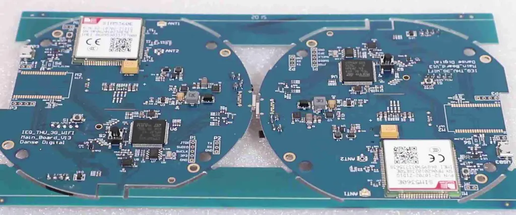
Altium Designer provides flexibility in board design, allowing for boards of various shapes and types, such as rigid, rigid-flex / pure flex. A rigid-flex design can accommodate many layer stack-ups, with the option to create additional coverlays. Components integrated on the internal routing layer, maximizing the use of space. 

With support for up to thirty-two signal layers and sixteen plane layers, the board can be customized to meet specific requirements. To make things more flexible, you can divide plane layers into as many parts as you want. You can also create smaller areas within those divided parts if you need to.

Altium Designer offers 32 mechanical construction layers that can be repurposed for specialized manufacturing layers, such as defining glue dots.

 Additionally, the board’s shape can be created externally and loaded into the printed circuit board editor using file formats such as DWG, DXF, or STEP. It allows for precise customization of the board shape, enabling designers to meet specific project requirements.

ยท A Flexible Workspace with groove PCB and Polar Grids

The designer has the flexibility to choose between metric/imperial units and work with either cartesian/polar grids. Additionally, it is possible to overlay many snap grids, which can be limited to objects or components only. The board size can vary significantly, ranging from minuscule to as large as 100×100 inches. Furthermore, design objects can be created as small as 0.001mil.

In addition to the grid alignment system, there is a helpful hotspot snap feature that can override the snap-to-grid and attract the cursor to the hotspot of an object when it’s within a user-defined range. This tool makes it easier to work with objects that aren’t lined up perfectly, like connecting wires to the pins of a part that’s measured in inches on a board that’s measured in millimeters.

In addition, the program allows you to customize where objects will snap, and it also provides guides to help you align objects in a specific direction. All of these features are valuable tools for achieving precise object placement.

How to Make groove PCB in Altium penalization?

FULL PCB MANUFACTURING Quote

As the electronics industry continues to evolve, many products within this sector have established complex upstream & downstream support enterprises. This industrial chain is naturally formed in a specific environment, which includes mature product design, manufacturing, design, packaging, assembly testing, and wholesale channels. As a result, the link between design & manufacturing is crucial, and the two are interdependent.

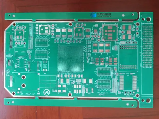
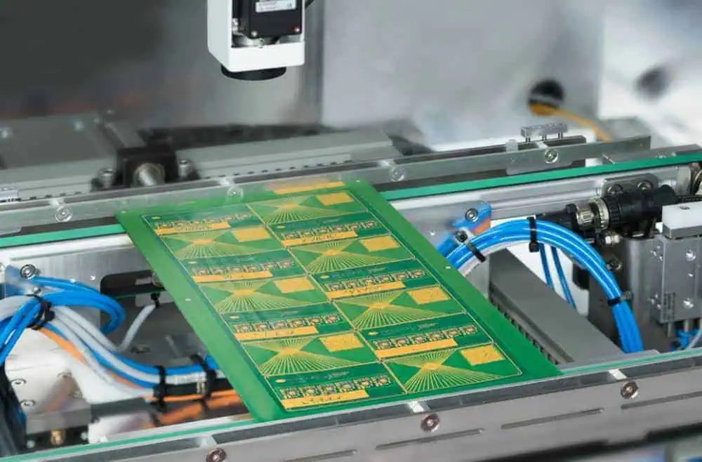
The processing of PCB boards is a crucial component of electronic product development and manufacturing, from design completion to production. Most of the plain circuit boards that PCBs work on are put together using machines that place electronic components on them.

As electronic products evolve towards smaller and lighter designs, a new problem arises. PCB manufacturing is well-suited for creating small boards, but when it comes to prototype PCB assembly, placement machines become a challenge. It is especially true for electronic components just some centimeters square in size, as the small area makes it challenging to assemble the product on the placement machine. It can create significant issues, particularly in the manufacturing line.

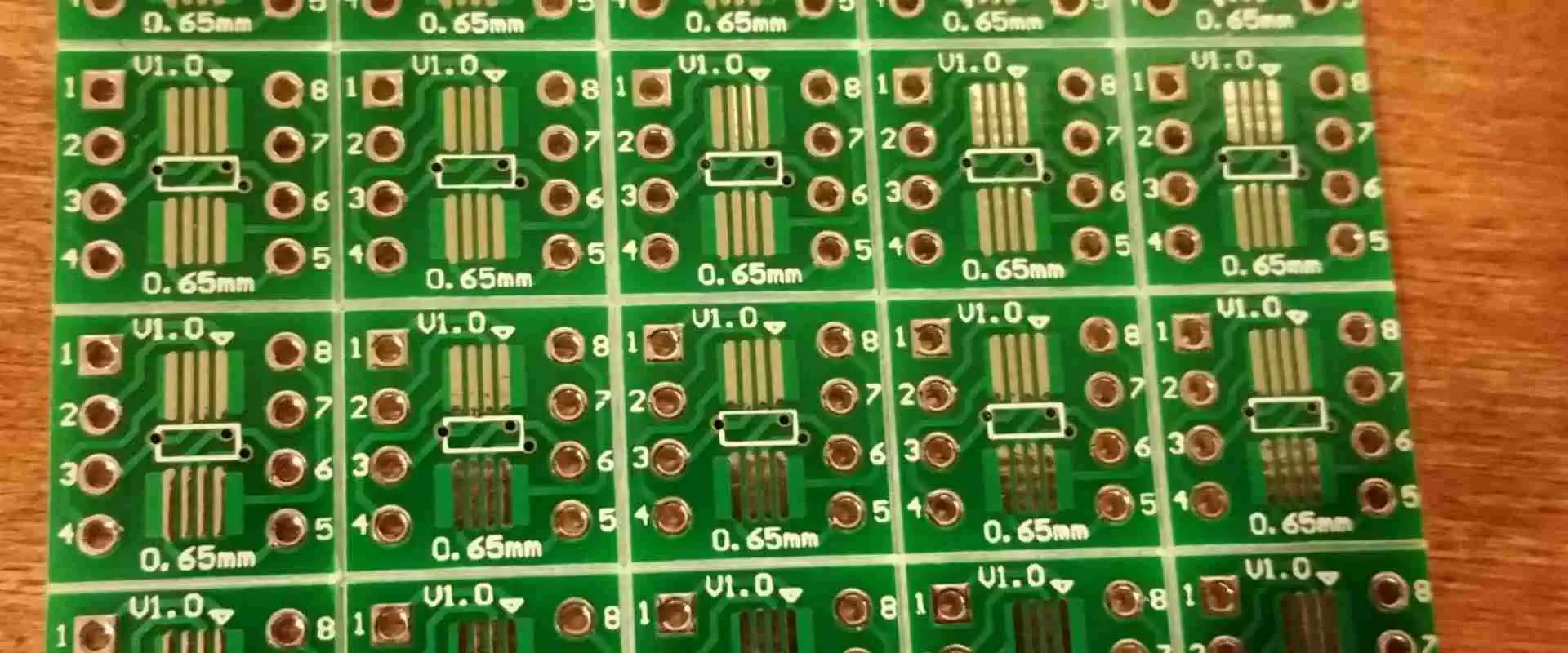
To address this issue, it becomes necessary to create a small printed circuit board that can be assembled in an area that meets the assembler’s needs or utilize a panelization method easier for SMT assembly, such as using a yin & yang board. Typically, manufacturing board factories offer panelization services. Still, by utilizing the Electronic design automation (EDA) software in the design process, designers can more clearly convey their intentions and reap several benefits, including:

  1. Enables creation in the desired orientation.
  2. The panelized layout is linked to the source circuit board, and any changes made to the source board are automatically reflected in the panelized circuit board.
  3. Allows for the combination of multiple different boards.
  4. Supports the use of yin & yang boards. 

How to put different Circuit Boards together?

Rotation Panelization

To combine different PCBs, select a printed circuit board file and arrange it in an array. Then, choose another printed circuit board file and arrange it similarly.

It is important to note that when combining different PCBs, the no. of layers & thickness settings of each PCB must be identical to ensure successful processing.

To make a yin & yang board, utilize the panel function to arrange a set of boards, then arrange another set of boards in the same way. Once this is done, choose the mirror function. It is important to note that the yin & yang boards should have identical layer thicknesses to be successfully combined and processed.

In addition to Altium Panelize, we can also provide a guide for penalizing PCBs using EasyEDA, Eagle, and KiCad software. If interested, we can allocate time to create a detailed guide for each program.

What is V Groove PCB?

V-groove printed circuit boards result from the splitting process of PCBs, which involves cutting the boards and leaving some material to hold them together. In the final stages of production, the V-groove printed circuit boards are profiled and separated from the production panel, either by routing / V-cut scoring. When manufacturing V-groove printed circuit boards, specific rules must be followed to ensure proper production.

Rules for manufacturing groove PCB

  •        Make sure that the board has a spacing of 0mm.
  • Keep the spacing between the outline & V-scoring line at 0.35mm.
  • The V-scoring line must be straight and either horizontal or vertical.
  • The V-groove printed circuit boards should have a minimum size of 75 x 75 mm and a size of 450 x 1245 mm.

Panelization Methods

Various methods exist for penalizing breakaway tab printed circuit boards, each with advantages and disadvantages. The design of the board and the panel itself typically play a significant role in determining the most suitable method for panelization. It is essential to consider these factors when deciding which approach to use.

  • Components: The placement of components on a PCB is just as critical as the choice of components themselves, particularly for sensitive connectors & components that can significantly impact the optimal panelization & breakout method.
  • Design: When determining the optimal panelization method, the board’s layout is the most crucial factor. The clearance between the edge of the board and its components may render some methods less suitable than others.
  • Materials: The materials used in mouse-bites printed circuit boards can affect the choice of the best panelization method. Certain materials are prone to splintering during the procedure of breakaway, which limits the suitable methods. The Breadth of the circuit board is also a critical factor. Thin boards are more likely to break during assembly, while thick boards may pose challenges during the breakaway process.

Why Your PCB Needs Fiducial Marks: Placement & Design Tips

In the modern printed circuit board (PCB) manufacturing, precision is paramount. Every component must be placed with utmost accuracy to ensure the final product functions as intended. This is where fiducial marks come into play. These small but crucial elements are the unsung heroes of PCB assembly, guiding automated machines to place components with pinpoint accuracy. In this comprehensive guide, we’ll explore the ins and outs of fiducial marks, their importance in PCB manufacturing, and how to implement them effectively in your designs.

What is a Fiducial Mark?

Fiducial marks, often simply called fiducials, are small, precisely placed features on a PCB that serve as reference points for automated assembly equipment. These marks are typically circular or cross-shaped and are made of bare copper with a protective coating to prevent oxidation.

Key Characteristics of Fiducial Marks:

  • Usually circular or cross-shaped
  • Made of bare copper
  • Coated to prevent oxidation
  • Precisely placed on the PCB
  • Act as reference points for assembly machines

Fiducial marks are essential in ensuring that components are placed accurately on the PCB during the assembly process. They provide a consistent reference point that assembly machines can use to orient themselves and make necessary adjustments.

Read more about:

How Does a Fiducial Mark Help in Manufacturing?

Fiducial marks play a crucial role in the PCB manufacturing process, particularly during the automated assembly stage. Here’s how they contribute to the production of high-quality PCBs:

1. Machine Orientation

Automated pick-and-place machines use fiducial marks to orient themselves relative to the PCB. This ensures that the machine knows exactly where it is on the board at all times.

2. Compensation for Misalignment

Even slight misalignments in board positioning can lead to significant errors in component placement. Fiducial marks allow machines to detect and compensate for these misalignments.

3. Improved Accuracy

By providing precise reference points, fiducial marks enable assembly machines to place components with high accuracy, often within fractions of a millimeter.

4. Consistency Across Boards

Fiducial marks ensure consistency in component placement across multiple boards in a production run, leading to more reliable and uniform products.

5. Error Reduction

The use of fiducial marks significantly reduces the likelihood of errors in component placement, thereby minimizing defects and improving overall product quality.

How Do I Add Fiducials to My Boards?

PCB Fiducial Mark

Adding fiducial marks to your PCB design is a crucial step in ensuring accurate assembly. Here’s a step-by-step guide to help you incorporate fiducials into your boards:

  1. Determine the Number of Fiducials: Decide how many fiducial marks you need based on your board’s size and complexity. Most designs require at least three fiducials.
  2. Choose Strategic Locations: Place fiducials in corners or along edges where they won’t interfere with components or traces.
  3. Use Your PCB Design Software: Most PCB design software packages have built-in tools for adding fiducial marks. Look for options like “Add Fiducial” or “Place Fiducial Marker.”
  4. Set the Correct Size: Typically, fiducial marks should be 1mm to 3mm in diameter. Consult with your PCB manufacturer for their specific requirements.
  5. Ensure Proper Clearance: Leave ample clearance around each fiducial mark to ensure it’s easily recognizable by assembly machines.
  6. Verify Placement: Double-check that your fiducials are placed correctly and don’t interfere with other elements on the board.
  7. Include in Manufacturing Files: Make sure your fiducial marks are included in the Gerber files you send to your PCB manufacturer.

Remember, the exact process may vary depending on your PCB design software, but these general steps should guide you in adding fiducials to your boards effectively.

Types of Fiducial Marks

Fiducial marks come in various types, each serving specific purposes in PCB assembly. Understanding these types can help you choose the most appropriate fiducials for your design. Let’s explore the different types of fiducial marks:

1. Panel Fiducial Markers

Panel fiducial markers are used when multiple PCBs are manufactured on a single panel. These fiducials are placed on the panel itself, outside the boundaries of individual boards.

Key Features:

  • Located on the panel, not on individual PCBs
  • Used for initial alignment of the entire panel
  • Typically larger than board-level fiducials

2. Global Fiducial Markers

Global fiducial markers are placed on individual PCBs and serve as primary reference points for the entire board.

Key Features:

  • Usually placed in opposite corners of the PCB
  • Used for overall board alignment
  • Essential for accurate component placement across the entire board

3. Local Fiducial Indicators

Local fiducial indicators are used for precise alignment of specific components or areas on the PCB.

Key Features:

  • Placed near critical or high-precision components
  • Provide additional reference points for localized accuracy
  • Particularly useful for fine-pitch or BGA components

4. Round or Dot Fiducial Marks

Round or dot fiducial marks are the most common type, featuring a simple circular shape.

Key Features:

  • Easy to create and recognize
  • Typically 1mm to 3mm in diameter
  • Provide a clear, unambiguous reference point

5. Crosshair Fiducial Marks

Crosshair fiducial marks feature intersecting lines forming a cross or plus sign.

Key Features:

  • Offer precise centering capabilities
  • Useful for high-precision applications
  • Can be more challenging to manufacture than round fiducials

6. Copper Fiducial Marks

Copper fiducial marks are created using the copper layer of the PCB.

Key Features:

  • Typically covered with a solder mask to prevent oxidation
  • Provide good contrast for optical recognition
  • Cost-effective and easy to implement

7. Grid Pattern Fiducial Marks

Grid pattern fiducial marks consist of multiple fiducials arranged in a grid layout.

Key Features:

  • Useful for large or complex boards
  • Provide multiple reference points across the board
  • Enable more precise alignment and component placement

8. Corner Fiducial Marks

Corner fiducial marks are specifically placed at the corners of the PCB.

Key Features:

  • Typically used in sets of three (three corners)
  • Provide reference points for overall board orientation
  • Essential for initial alignment in the assembly process

By understanding these different types of fiducial marks, you can make informed decisions about which ones to use in your PCB design, ensuring optimal alignment and component placement accuracy during the assembly process.

Advantages of Using Fiducial Marks for PCB Assembly

Incorporating fiducial marks into your PCB design offers numerous benefits that contribute to improved manufacturing efficiency and product quality. Let’s explore the key advantages:

1. Enhanced Accuracy in Component Placement

Fiducial marks provide precise reference points for automated assembly equipment, resulting in highly accurate component placement. This accuracy is crucial for:

2. Increased Production Efficiency

By enabling automated equipment to quickly and accurately align boards, fiducial marks help to:

  • Reduce setup time
  • Increase throughput
  • Minimize production delays

3. Improved Quality Control

Fiducial marks contribute to better quality control by:

  • Ensuring consistent component placement across all boards
  • Reducing the likelihood of misaligned components
  • Facilitating easier visual inspection

4. Cost Reduction

While adding fiducial marks might seem like an extra step, they actually help reduce costs by:

  • Minimizing rework and repairs
  • Reducing scrap rates
  • Improving overall yield

5. Compatibility with Advanced Manufacturing Techniques

Fiducial marks support advanced manufacturing processes, including:

  • High-speed automated assembly
  • Flip-chip technology
  • Micro-BGA placement

6. Flexibility in Design

Fiducial marks offer design flexibility by:

  • Allowing for more complex board layouts
  • Supporting a wider range of component types and sizes
  • Enabling tighter component spacing

7. Enhanced Reliability

The precision offered by fiducial marks leads to enhanced product reliability through:

  • Reduced risk of short circuits from misaligned components
  • Improved solder joint quality
  • Consistent performance across all manufactured boards

8. Simplified Troubleshooting

In case of assembly issues, fiducial marks can:

  • Help identify misalignment problems quickly
  • Facilitate easier board-level repairs
  • Aid in root cause analysis of manufacturing defects

By leveraging these advantages, PCB designers and manufacturers can produce higher quality boards more efficiently, leading to improved product performance and customer satisfaction.

Fiducial Mark Design Guidelines

Designing effective fiducial marks is crucial for ensuring their functionality in the PCB assembly process. Here are some key guidelines to follow when incorporating fiducial marks into your PCB design:

1. Shape

The shape of your fiducial marks plays a significant role in their effectiveness:

  • Recommended: Circular shapes are most commonly used and easily recognized by assembly equipment.
  • Alternative: Square or diamond shapes can also be effective but may require specific machine settings.
  • Avoid: Complex or irregular shapes that may be difficult for machines to interpret.

2. Size

The size of fiducial marks is critical for accurate recognition:

  • Diameter: Typically between 1mm and 3mm.
  • Consistency: Maintain uniform size across all fiducials on the board.
  • Machine Compatibility: Consult with your assembly house for their specific size requirements.

3. Material

The material used for fiducial marks affects their visibility and durability:

  • Copper: Most commonly used due to its conductivity and contrast with the board surface.
  • Coating: Apply a protective coating (e.g., ENIG) to prevent oxidation.
  • Avoid: Using solder mask as the sole material for fiducials, as it may not provide sufficient contrast.

4. Clearance

Proper clearance around fiducial marks ensures they are easily recognizable:

  • Solder Mask Clearance: Maintain a solder mask clearance of at least 0.5mm around the fiducial.
  • Component Clearance: Keep a minimum distance of 5mm between fiducials and nearby components or board edges.
  • Copper Pour Clearance: Ensure no copper pour or traces within 2mm of the fiducial mark.

Additional Design Considerations

  1. Quantity: Include at least three fiducial marks per board for optimal alignment.
  2. Placement:
    • Position fiducials in at least two opposite corners of the board.
    • For larger boards, consider adding additional fiducials along the edges.
  3. Symmetry: Avoid symmetrical placement that could lead to 180-degree rotation errors.
  4. Visibility: Ensure fiducials are visible and not obscured by components or other board features.
  5. Consistency: Use the same design for all fiducial marks on a given board.
  6. Documentation: Clearly document fiducial marks in your design files and manufacturing specifications.
  7. Verification: Double-check fiducial mark placement and specifications before finalizing your design.

By adhering to these design guidelines, you can ensure that your fiducial marks effectively serve their purpose in guiding automated assembly equipment, leading to more accurate and efficient PCB production.

Conclusion

Fiducial marks are indispensable elements in modern PCB design and manufacturing. Their role in ensuring precise component placement, improving production efficiency, and enhancing overall product quality cannot be overstated. By understanding the different types of fiducial marks, their advantages, and following best practices in their design and implementation, PCB designers can significantly improve the manufacturability and reliability of their boards.

Remember, while fiducial marks may seem like small details, they have a big impact on the success of your PCB production. Always consult with your PCB manufacturer to ensure your fiducial mark design aligns with their equipment capabilities and requirements. With proper implementation of fiducial marks, you’re setting the stage for efficient, high-quality PCB assembly that meets the demanding standards of today’s electronics industry.

Whether you’re working on a simple two-layer board or a complex multi-layer design, incorporating well-designed fiducial marks is a step towards manufacturing excellence. So, the next time you’re laying out a PCB, give fiducial marks the attention they deserve โ€“ your assembly team and end-users will thank you for it.

What is a DIP Switch PCB in Electronics?

DIP Switch PCB

DIP literally means โ€œDual In-Line Package.โ€ It is an electronic term used for types of a switch. DIP switch is a group of small-size manual switches for electronics. They are specially designed to be grouped with other printed circuit boards. The term DIP either refers to a single switch, a unit of multi-switch, or the complete unit. 

DIP switches are essentially used to modify a device’s operating mode by allowing users to manage the electric current that flows around a PCB, electronic accessory, and expansion card. 

DIP switches provide the user with the ability to tailor the behavior of the electronic equipment in question when mounted on a PCB along with other components, enabling complete leverage over the specific task the device will conduct in a variety of applications and defined scenarios. DIP switches are commonly displayed as a series of small toggle (on/off) switches installed consecutively on a piece of high-temperature thermoplastic polymer, much like a number of miniature traditional light switches.

A group of DIP switches nearly always requires considerable dexterity from the user to toggle every switch between the state of on and off because they are often quite small as a whole component. In actual use, this function is frequently carried out with the tip of a pointed pencil or another appropriately shaped tool because individual switches are typically too small to be operated with a finger.

DIP switches are often widely used, reasonably priced components that make it easy to choose and switch between different hardware or device configurations. DIP switches have the drawback of requiring the user to physically open the device in order to access the PCB and then manually activate the switches from there. However, they are typically far less expensive than alternatives like programmable chips or programming control panels.

This article gives you a detailed insight into the types, forms, and functions of a group of DIP switches and the various types and varieties of devices and applications available in the market.ย 

Uses of DIP Switch PCB

pin switch

Due to the downscaling trend and the decreasing costs of other equivalent solutions, DIP switches are less popular than they previously were. Nonetheless, they continue to be utilized in a variety of test circuits and industrial applications. 

This is due to the fact that physical DIP switches provide a very affordable choice for system control that is also incredibly simple to connect to an existing Printed circuit board or prototype circuit model. DIP switches can significantly decrease the need for extra hardware to conduct a wider range of output jobs by providing a quick and handy way to physically observe the settings that are currently chosen without turning the system on first.

Application of DIP Switch PCB

In modern circuits and devices, the most widely used applications of DIP switches include the following.

The setting up of numerous possibilities for Computer hardware and accessories. This comprises expansion modules, motherboards, hard drives, video cards, modems, as well as other add-ons or auxiliary parts. There are still many garage doorway systems that use DIP switches.

They’re frequently used in universal remote controllers to stop electrical interference from causing accidental device control. For each pair of receivers and transmitters in this scenario, a distinct radio frequency will be configured using the DIP switch.

How does DIP Switch PCB Work?

FULL PCB MANUFACTURING Quote

Conventional surface-mounted DIP switches are offered as an arrangement of straightforward two-terminal (1/0 or on/off) mechanical switches that have been constructed inside a thermoplastic polymer block container. Although technically, they are just an alternative to the traditional jumper; they are frequently referred to as “jumpers” despite the fact that their general purpose is extremely similar.

The “dual in-line” part of the acronym relates to how the contact pins on the underside of the DIP switch block, which connect to the PCB or prototype directly, are arranged. They are placed in two parallel lines, hence the name “dual in-line.” In general, a given module will have twice quite so many contact wires as switches.

When choosing a certain device function and needing to toggle many switches to get the desired output mode, DIP switches come in handy. Among the most frequent uses for a DIP switch is on the motherboard of a computer, where different configuration options can be accessible by flipping various switches.

A typical DIP switch could include one, two, four, seven, eight, ten, sixteen, or more toggle, slide, rocker, and rotatory slide installed on one tiny block. Although DIP switches are simple parts, their value lies in the fact that by placing numerous toggles in parallel, each one can be individually switched to the 1/0 position, potentially opening up a vast array of possible combinations to explore.

With a typical DIP switch matrix, every single toggle is disconnected from the others. A flexible suspension underneath the switch reacts to the motion of the rocker or slider and bends gently up or down in order to shut or open a passive contact below when a switch on such a DIP switch is shifted between its on and off settings. Correspond with a wide range of potential device outputs/functions.

As per their safe operational power, improved power quality, and voltage, DIP switches are generally divided into groups for various functions and applications. Users must follow and adhere to the manufacturer’s guidelines while using a specific DIP switch in order to avoid issues like a self-welded switch and electric curving while switching that could result in performance instabilities or device breakage.

Benefits of DIP Switch PCB

The following are just a few of the numerous advantages of DIP switch matrices in specific circuits, design procedures, and types of devices:

  1. For certain higher-end Dual In-line Package switch versions, gold contacts are frequently a choice, providing significantly improved durability and efficiency.
  2. They serve as a practical upgrade to more worn-out jumpers.
  3. Units range from 1 to 32 poles, providing a wide range of utility and versatility.
  4. In busy production operations, longer poles upon certain designs help save loading times.
  5. In order to place DIP switches on a Printed Circuit Board or prototype, their poles can easily be adjusted by being chopped to the appropriate level.

Conclusion

Although there has been a slight decline in the use of DIP switches in some contemporary applications due to the rising cost-effectiveness of application control panels as well as computer-controlled onboard chips, DIP switches still are viewed as a very appealing option in a variety of design workflows, device testing, and industrial settings.

Look for New Technology Now and Have Stretchable Circuit Board

stretchable circuit board

Most conventional or traditional PCBs are rigid, which means that when in operation, they shouldn’t bend. Stretchable and flexible PCBs are required because many applications require a board to repeatedly bend or flex, which is a requirement for many applications. On closer inspection, a wide variety of newly developed parts, gadgets, and electronic components strongly demonstrate mechanical stretch ability.

Some of these include uses for curved surfaces, like those in the automobile industry, or flexible connections, like those in mobile phones. This page provides examples of a variety of stretchable PCB-related topics, including their composition, characteristics, mechanism, benefits, applications, and expected future developments.

Design/Construction Of Stretchable Circuit Board

The substrate is Polyimide or Polyurethane, even though flexible PCB technology uses standard manufacture and subsequent assembly methods. Stretchable PCBs may be made with polyurethane or polyimide at a substantially lower cost than other materials. A large number of manufacturers use the following techniques to swiftly construct the substrate’s component parts.

Locally applied special coatings or interposers are the major methods used by manufacturers to strengthen the laminate. The most effective strategy, however, makes use of a technique called Stretch-Rigid. Stretch-Rigid connects two stiff boards without the need for a flexible PCB, as opposed to Rigid-Flex architecture, which performs less well.

The technology of Stretch-Rigid connects various rigid boards utilizing substrates that can be stretched and include integrated copper connectivity traces. Afterward, the electronic components are only soldered on such sturdy sections.

Advantages Of Stretchable Circuit Board

stretchable PCB board

Stretchable Printed Circuit Boards are specifically made to be more flexible and save space in order to accommodate mounting designs with high density and lower footprints. Moreover, it aids in simplifying the assembling process while also boosting dependability. In short, the only approach that guarantees electrical device mobility and downsizing is flexible PCBs.

Stretchable circuit boards provide a number of benefits that are worth highlighting. Stretchable PCBs, for instance, may be pushed, stretched, and twisted without putting the conductor in danger. Moreover, flexible PCBs allow for a variety of shapes and custom-packed sizes.

Not just that. Excellent electrical conductivity is offered by flexible PCBs. They have a low dielectric constant which allows for electrical signal transmission, and outstanding thermal characteristics, which facilitate cooling. Furthermore, unlike hard PCBs, stretchy PCBs can function effectively in high temperatures.

Due to fewer internal connections, stretchable PCBs offer better assembly output and dependability. Additionally, as this PCB was created or built for one-way assembly, there was a little mistake during construction. Stretchable boards may easily change locations while being permanently electrically connected to one another.

Some other effective benefits of using flexible PCBs rather than rigid PCBs are as follows:

  1. Outstanding Thermal conductivity
  2. It lets Weight and occupies less space
  3. Meet all the requirements of transformation due to flexibility.
  4. Enhanced reliability and repeatability
  5. Reduce the prices of the overall assembly.
  6. Goes with connectors
  7. Excellent electrical conductivity and high speed

Mechanism Of Stretchable Printed Circuit Board

FULL PCB MANUFACTURING Quote

Copper traces prevent the stretchy PCB substrate made of the thermoplastic polyurethane that manufacturers employ from spreading. This is due to the fact that copper isn’t really sufficiently bendable for these uses.

Producers bind RA copper foil or conventional ED on the polyurethane base using their own lay-up methods and specialized presses. After finishing this stage, they build the stretchy circuits using customary subtractive wet-etching PCB procedures.

Stretchability is reduced when polyurethane base and adhesive are added in many layers. Hence most stretchy Printed Circuit Boards are double-layered or have a maximum of four layers. To ensure a consistent elastomer design, manufacturers add polyurethane solder covers on completed Boards.

Stretchable PCBs are put together using standard, surface mounting parts that are soldered to the copper rails. The locations where the elements are positioned cannot be stretched since the pieces are stiff. Stretchable PCBs are essentially some tiny, rugged islands that house sparse SMD components. On stretchy substrates, some conductive paper foil is used to link these SMD components.

Designers gave the copper traces on the substrate a funnel form to guarantee that they may flex or twist without being damaged. The horseshoe forms are then alternately positioned at 180โ—ฆ c to enable them to wander along a route that straight markings would have followed. While alternative methods, including triangular forms, can stretch, they do so with high amounts of stress and with reduced dependability.

Due to the aforementioned, many manufacturers like the horseshoe form, leading most of them to standardize it.

Top Uses Of Stretchable Circuit Board

Flex-PCB-Antenna

Stretched PCBs are typically used in bending or irregularly shaped surfaces. These are some of the major applications for stretchy PCBs. It is clear that stretchy PCBs and such applications are both growing. On incorporated surfaces, such as implantable or wearables devices, a standard rigid PCB cannot be conveniently positioned or used.

Equipment and parts utilized in biological applications, safety, sports, and leisure frequently have asymmetrical shapes. A PCB must adhere to the form necessary for effective integration, even with such erratic forms. Stretchable circuits may readily adapt to any area, whilst flexible circuit shapes like a cone or cylinder can be created.

Having stated that, stretchy PCBs are utilized in a wide range of applications, including consumer garments, precise positioning, and medical devices. For instance, integrated sensors on stretchy PCBs can be used to monitor pressure inside the sole of a shoe. By gathering user information based on unrestricted mobility, they do this.

Moreover, since they have pressure sensors placed in them that can accurately assess the contact pressure, stretchable PCBs are inserted within bandages. It is extremely useful to be able to monitor contact pressure, particularly when treating open wounds.

Conclusion

Stretchable PCBs are used extensively in a wide variety of electronic gadgets to give comfort as one of their distinctive features. There are several benefits that flexible PCBs may provide that rigid PCBs cannot. Stretchable PCBs is expected to see unprecedented levels of utilization based on predicted future trends. 

Understanding the Arduino Integrated Development Environment

Arduino Integrated Development Environment

The advent of the Arduino software as well as Arduino boards (the hardware) has made electronics development simpler. With the aid of additional parts, this set facilitates the construction of interactive and digital gadgets.  

Previously, we discussed Arduino boards. However, in this tutorial, we’ll define Arduino software and explain how to utilize it.

What Does Arduino Integrated Development Environment?

In order to write a code, the text/code editor is required. A compiler is then required to translate the written code into binary files or machine code, which the microcontroller then can understand. Programming software is also required in order to load the firmware files to the microcontroller.

An Integrated Development Environment, which can be described simply as Arduino Software, is what we refer to when we are combining all of these functionalities with some extras like console support, debugging support, etc.

The development IDE that is suited for Arduino boards is known by the moniker Arduino IDE. It has a compiler, code editor, serial console, programmer, serial plotter, as well as many other capabilities that are fully featured. Also, it is straightforward and simple to use.

The Arduino IDE can be described as a cross-platform and can function on Microsoft, Linux, and Windows operating systems. Additionally, you may program these boards utilizing the C/C++-derived Arduino Language and Arduino IDE.

Writing code and uploading it onto the circuit board while offline is simple with Arduino Software. Every Arduino board is compatible with this software.

Arduino IDE is now available in two different versions: 1.x.x and 2.x. IDE 2.x is a brand-new major update that outperforms IDE 1.x.x in terms of speed and power. It also has more sophisticated capabilities to aid users in their debugging and coding in addition to more contemporary editor and a responsive user interface.

More Information About the Arduino IDE

Arduino IOT

Write, compile, and upload code to practically all types of Arduino Modules using the Arduino IDE, an open-source program created by Arduino.cc.

Due to the official Arduino software’s ease of use, even a layperson with no previous technical training can get started with it.

It operates on Java Platform, which has built-in functions as well as commands that are essential for debugging, modifying, and generating the code, and is compatible with all forms of operating systems, including MAC, Linux, and Windows.

Several Arduino modules are available, including the Mega, Uno, Leonardo, Micro, and many others. On the boards of each, there is a microcontroller which is properly programmed as well as takes data in form of a code.

The primary code, often referred as the sketch, written on a IDE platform would eventually produce a unique Hex File, that is transported to and uploaded into the board’s controller.

The Compiler and Editor are the two primary components of the Arduino Integrated Development Environment. The Editor is responsible for the compilation and the uploads of the code to that Arduino Module, while the Compiler is necessary for the writing of the necessary code.

Both C++ and C are supported in this environment.

Installing the Arduino IDE

The installation of the Arduino IDE is rather simple. To obtain the most recent edition of the Arduino IDE, visit Arduino IDE. For several operating systems, including Windows, Linux, and Mac, there are numerous versions available.

Additionally, there are now two versions of the IDE: 1.x as well as 2.x. In this tutorial, we’ll focus on Classic 1.X version. In essence, both offer nearly identical functionality having its different GUI and a few extra capabilities, including automatic code completion.

  • Click the aforementioned link to download any installer for the OS system.
  • Open that .exe file after the download is complete.
  • Click “Next” to proceed after accepting the license agreement and deciding whether or not to install the IDE for all users.
  • Click “Install” after deciding whether you wish to alter the default installation location for the IDE or leave it alone.
  • After the installer has completed installing, click “Close.”

Arduino IDE Basics

Double-clicking of the shortcut of the Arduino on your desktop or Start Menu will start your Arduino IDE after it has been installed. This Arduino IDE would now be launched. The interface of your Arduino IDE is displayed below.

Choosing the appropriate Board on the Arduino

Let’s choose the appropriate board now. Before compilation, it is crucial to choose the correct board since this compiler will utilize it during the compile instructions. To accomplish that, choose your board out from list by clicking on “Tools” then “Board” -then on “AVR Boards”.

Choose Arduino Serial Ports

It’s crucial to choose the correct serial port for the Arduino board’s connection. You will not have the ability to upload this code to your board if you don’t do this. To achieve that, pick the appropriate COM port by clicking on “Tools” and then “Port.”

Disconnect your Arduino board out from USB port then revisit the menu if you have several COM ports available and you’re unsure of the one to use. This COM port which vanished will really be the right COM port. Select this USB port by reconnecting the Board onto it.

Different Sections of the Arduino IDE

There are three basic divisions of the IDE environment. These include menu bar, the text editor, and the output pane.

The Menu Bar: This top bar is referred to as the Menu Bar and offers the following five options.

File: With this, you can create a brand new window or reopen an already existing one to write the code. The additional categories into which the option of the file is divided are displayed.

Edit: Used to copy and paste the code plus additional font modifications.

Sketch: Is used for programming and compiling.

Tools are primarily employed in testing projects. A bootloader is burned to the fresh microcontroller using the Programmer part of this panel.

Help – If you are unsure about the software, full assistance is offered, from starting up to troubleshooting.

The Text Editor: This same primary screen, which is located underneath the menu bar, serves as a straightforward text editor for entering the necessary code.

Output window: The output pane at the bottom of the main screen, which mostly displays the memory usage and programming mistakes, is referred to as the compilation state of a running code. Before uploading this hex file to the Arduino Module, you must correct those problems.

Arduino Board Types

Arduino Uno

Compared to earlier Arduino boards, the creation of the Arduino UNO boards is said to be new. This board offers a variety of helpful features, which assists the user in utilizing this in projects.

Atmega16U2 microprocessor used by Arduino UNO helps to speed up data transfers and has more memory than other board types.

LilyPad Arduino

This LilyPad Arduino can be regarded as another sort of Arduino board which is made to work with e-textile and wearable project integration. This board’s spherical form reduces snagging and makes it simple to connect it to other gadgets.

The Atmega328 microcontroller and Arduino bootloader are both used in this device. The design of this board is simple and compatible because it incorporates relatively few external components.

Arduino Mega

Arduino Mega is regarded as a microcontroller because it contains an Atmega2560. It has a total of 54 output and input pins, of which 14 of the pins are used for PWM output, while 4 are for hardware ports, and 16 for analog inputs. One USB port, an ICSP header, a power jack, and a REST pin are also present on the board.

Arduino Leonardo

The board is regarded as a microcontroller because it contains an Atmega32u4. It has a total of 20 digital output and input pins, of which 7 are used for PWM while 12 of them are ffor analog inputs. In addition, the board has a power jack, a micro USB port, and a RESET button. There are extra pins that function as a 16 MHz crystal oscillator.

Arduino Red board

Another variety of an Arduino board which can be programmed using Arduino IDE and a small USB connection is Arduino Red board. You don’t have to modify its security settings in order for this board to function with the operating system of Windows 8. This Red board connects to other devices using the FTDI and USB chips.

Arduino Shields

Considered to be pre-built circuit boards, Arduino shields are utilized for connecting to other types of Arduino boards. Arduino shields are mounted on the top of the Arduino boards as well as improve their connectivity to the internet, their capacity to control a motor or an LCD, and their ability to establish any wireless connection.

Conclusion

By now, you understand what the Arduino Integrated Development Environment is all about. Beginners and more experienced users can both easily utilize this Arduino software. It is used to create interactive prototypes and begin with robotics and electronics programming.

The C/C++ programming languages are supported by the Arduino software (denoted as IDE), which works with multiple operating systems like Mac OS, Linux, and Windows.

How Arduino Python Projects are Impacting Electronic Circuit Design

Arduino Python Projects

The utilization of microcontrollers keeps increasing. These components have been around and their use range from common household appliances to complex machines. Electrical engineers and technicians are familiar with these components.

The advent of Arduino has made it easy for developers to gain more access to electronic application design. Our focus here is on Arduino Python projects.

What is Arduino Platform?

Arduino comprises hardware and software that enables the development of interactive electronics projects. The emergence of this open-source platform got the attention of many professionals across several fields, thereby contributing to the Maker Movement.

Arduino is now one of the primary platforms for MVPs development and electronic prototyping with the growing popularity of the concept of IoT and Maker Movement. Also, the Arduino platform features its own programming language. This language is quite similar to C++. However, Arduino can be used with high-level programming language like Python.

Using Arduino with Python

In fact, Arduino as an open source platform functions very well with Python, particularly for applications need to be integrated with sensors. The combination of Arduino and Python offers an effective learning environment which helps developers to achieve great electronics design.  Python is a high-level programming language designed for applications like data analysis, scientific computing, web development and more.

This programming language is simple, readable and very flexible. Due to its features, Python gained popularity among experienced programmers and beginners. The integration of Python with Arduino enables engineers and developers to optimize the easy-to-use and powerful libraries offered by the Python ecosystem.

Another benefit of integrating Python with Arduino is that it enables developers to prototype and test their ideas easily. With this, you donโ€™t need to compile and upload code to the Arduino every time there is a change. Python features an active community of developers and users. Therefore, there is a wide range of resources and documentations. You can as well get support online.

If you are quite familiar with basics of Python, then you can use Python to control Arduino. The Arduino platform comprises software and hardware products. Here, we will integrate Arduino hardware and Python software to learn about basic circuits.

Arduino Hardware

Users need to hook up electronic components to assemble the circuits. You will need the following components

  • A breadboard
  • A push button
  • An Arduino Uno
  • A 470 Ohm resistor
  • Different sizes and colors of jumper wires
  • A standard LED
  • A 10 KOhm potentiometer

Arduino as a project comprises several modules and boards for various purposes. The Arduino Uno is the most commonly used board in the Arduino family. Furthermore, the 470 Ohm resistor and 10 KOhm resistor are crucial. You will identify resistors by their colored stripes.

The breadboard in the list above is crucial for assembling the circuits. You need to get a breadboard when working with Arduino.

Arduino Software

FULL PCB MANUFACTURING Quote

Some software applications need to be installed. Arduino was specially designed to enable the programming of boards. Connect the board to your computer, install Arduino IDE, configure the settings of the board, write code, and press a button on the Integrated Development Environment (IDE).

You need to download the right version for your OS in order to install the IDE on your computer. Follow these instructions for installation:

  • If your device is macOs, you can check the Arduino install guide for OSX to learn how to install Arduino IDE.
  • If your device is Linux, you will need to include your user to groups. This will help you to integrate the serial port for programming Arduino.
  • If your device is Windows, download the important drivers by using the Windows installer. To get more information, you can follow the guidelines in the Arduino Documentation.

How to Use Arduino with Python

Arduino makes use of a programming language that is quite similar to C++. You can take some approaches to Integrate Arduino with Python. A great idea to use is to run the main program on your personal computer and make use of the serial connection to interact with Arduino via the USB cable.

You need to design a protocol to enable interaction between Arduino and PC. For instance, consider a protocol that has messages like SET PIN 11 Low or VALUE OF PIN 13 is HIGH. The SET PIN 11 LOW instructs Arduino to set the output pinsโ€™ states. Also, the VALUE OF PIN 13 IS HIGH informs the personal computer about the digital input pinsโ€™ status.

You can design an Arduino sketch to send some messages to the personal computer with a defined protocol. Also, you can update the pinsโ€™ states. You could write a program on the PC to control the Arduino via a serial connection. This will be done according to the protocol youโ€™ve designed.  You can integrate any language and libraries of your choice, this includes the PySerial library and Python.

Well, you can do all of this with standard protocols. One of such protocols is Firmata. With this protocol, you can create a serial communication format with which you can read analog and digital inputs. Also, you can send data to analog and digital outputs.

The Arduino Integrated development environment (IDE) features existing sketches that will helps Arduino via Python. On your personal computer, the adoption of the protocol is in several languages, this includes Python.

How to Upload the Firmata Sketch

It is important you upload a Firmata sketch before writing Python to drive Arduino. This will help you have a control over the board. You can find the sketch in the built-in example of Arduino IDE. Go to the โ€œFile menuโ€, click โ€œExamplesโ€, and choose โ€œFirmataโ€, and then click on โ€œStandardFirmata.โ€

The sketch will be available in a new IDE window. You can upload the sketch by following these steps:

  • Plug the USB cable
  • Choose the right port and board on the IDE
  • Click on Upload

After you have completed the upload, you will realize there is no activity on the Arduino. A program that can interact with the board via the serial connection will help you have control over the upload. Also, the pyFirmata package if you will be working with the Firmata protocol.

Asides from Arduino and Firmata, there are several ways you can use Python in microcontrollers. These includes MicroPython, SBCs, and pySerial.

How to Use a Sensor to Create a Notification

One way to effectively use Arduino with Python is Firmata. However, it can be costly to get a PC to run the application. In some cases, this approach may seem impractical. Arduino and Firmata are perfect for collecting and sending data to a PC with external sensors.

Here, you will need a push button linked to your Arduino. This will work like a digital sensor and cause a notification to appear. The push button can function as a door sensor that causes an alarm notification. For instance, you will use Tkinter to showcase the notification on your personal computer. A message box will appear when you press the button.

Step by Step Guide on How to Program Arduino with Python

Install Python IDLE

You will need to visit the Python website to download Python IDLE. If you have it already installed, you can skip this step.

Install PySerial

PySerial reads and writes serial data to Arduino. It is a Python API module. You will need to download PySerial and install on your PC.

Python Code

The python code is very important since you will be needing a simple program to enable Python send data to the serial port.

Arduino code

To enable Arduino to connect with Python, you need to know which COM port the Arduino is on. The Arduino programming environment carries out this task.

Some Arduino Python Projects

There are some projects you can carry out on Arduino with Python. Some of the Arduino Python projects are mentioned below

Face tracking

This is one of the most impressive Arduino Python projects. Here, you will learn how to use your face to control a pan-tilt servo mechanism. You will make use of OpenCV to enable facial recognition and then Python will be able to send position data to Arduino. Serial connects the Arduino and  maps the location data to have control over the pan-tilt servos. This Arduino Python project will surely impress you.

Control Arduino with Python

This particular project makes Arduino a Serial device. You will make use of Python script to write on the Arduino instead of integrating the Serial monitor to transmit a bit of data. Arduino will switch on and off the LED. This is a great starting point for advanced and complex Python projects for controlling Arduino hardware.

Conclusion

The combination of Arduino and Python offers an effective learning environment which helps developers to achieve great electronics design.  If you are quite familiar with basics of Python, then you can use Python to control Arduino.  Arduino platform comprises software and hardware products. The integration of Python with Arduino enables engineers and developers to optimize the easy-to-use and powerful libraries offered by the Python ecosystem.

What are the Requirements for Blockchain Hardware?

Blockchain Hardware

All complex systems require the appropriate tools, architecture, as well as infrastructure to operate correctly. Infrastructure for enterprise blockchains is also common. Therefore, in order for a blockchain proof-of-stake network to function, software implementations, nodes, as well as hardware or cloud-based systems are required.

PaaS (platform-as-a-service) providers of blockchain infrastructure oversee and regulate access to this fundamental infrastructure needed to run such systems, including data security and cloud storage, coupled with the infrastructure which enables blockchains, like nodes and dev tools. Let’s examine the blockchain’s technical foundation and security features.

How Does Blockchain Technology Work?

Blockchain technology is a platform for storing operational data across numerous databases present in connected networks with the help of peer-to-peer nodes. The term “digital ledger” is widely used to describe this kind of storage.

A decentralized ledger known as a blockchain copies and spreads transactions among different computers’ network participating. Blockchain is a data storage technique which makes it very hard or unfeasible to alter the network, hijack it, or otherwise compromised.

What Does Blockchain Infrastructure Mean?

QUICK TURN PCB ASSEMBLY

The infrastructure of the blockchain hardware serves as its base. The equipment or facilities which make blockchain technology operate efficiently are known as blockchain infrastructure. Blockchain is a hybrid of blockchain software and blockchain hardware. It encompasses more than just computer code.

The systems and components that support as well as enable the use of the blockchain technology are known as blockchain infrastructures. Running a node continuously is more crucial for blockchain compared to the blockchain development’s system requirements.

You need to have plans regarding the infrastructure resources in order to support the initial pilots and lay the basis for the scaling up when and if those pilots would go live in order to pilot the blockchain efforts effectively. Due to this, you need to think about how blockchain would impact the data center architecture and the effects it will have on your organization.

Requirements for Blockchain Infrastructure

Blockchain technology encompasses more than just novel types of software or databases. Therefore, a sophisticated and extensive infrastructure is required. The needed hardware and software for the blockchain infrastructure are listed below.

Blockchain Software Requirements

The following is a list of the program prerequisites:

Solidity

One language frequently utilized by the blockchain developers is solidity. To support the Virtual Machine of Ethereum, it was developed. In addition, JavaScript, Python, and C++ shape it.

The most widely used OOP and CIS framework for developing smart contracts is Solidarity. Using Solidity, blockchain developers may create applications that execute self-enforcing logic within smart contracts and keep a trustworthy and accurate log of any transaction. When creating contracts for crowdsourcing, voting, blind auctions, as well as multi-signature wallets, this is advantageous.

Geth

Geth can be accessed using the command line, an engaging console, or JSON-RPC server. Geth is employed for a variety of tasks, such as ether mining, token transfers, the development of different smart contracts, including looking up block histories. You can join any existing Blockchain and create your own after the installation of Geth. The nicest part is Geth’s ability to ensure things are done easier through the establishment of a connection onto the main net of Ethereum instantly.

Mist

FULL PCB MANUFACTURING Quote

The official wallet for Ethereum created by the Ethereum developers is called Mist. It is compatible with Linux (64-bit and 32-bit), Mac, and Windows (64-bit and 32-bit).  Although Mist is particularly well suited for creating smart contracts, you must download the entire Ethereum blockchain, that takes up over 1TB, since it is known as the complete node wallet. Because this is known as a one-time installation requirement as well as cannot be altered, it is also crucial to remember the Mist password. Solc

A command-line compiler for Solidity built on C++ is called Solc or Solidity Compiler. The primary goal is to convert Solidity scripts to a more comprehensible form for the Virtual Machine of Ethereum. Despite having syntax similar to JavaScript and being a condensed programming language that is loosely typed, Solidity’s smart contracts must be converted into any format that this virtual machine will be able to comprehend and interpret readily. This is one good reason why the solidity compiler is very useful.

There exists two different versions of Solc: the most recent Solc-js, that utilizes Emscripten in cross-compiling the initial source code of Solc from the C++ onto the JavaScript, as well as the initial Solc, which was developed in C++. Another application for Solc is offline compilation.

Remix

A Blockchain tool in developing and implementing smart contracts is called Remix IDE. A remix can be described as a Javascript tool that can be used by any current web browser in developing, testing, debugging, and deploying smart contracts that are solidity-based. Remix is well-documented and offers a simple Metamask connection process for connecting to Ethereum blockchain. Blockchain ganache, test net, BaaS (Blockchain-as-a-Service), MetaMask (wallet), as well as Truffle are among the additional software needs for the blockchain infrastructure.

Hardware Requirements for Blockchain

PCBA Conformal coating

High-performance PCs are the standard term used to describe blockchain hardware. Businesses need these sophisticated computers because they make it possible to execute jobs quickly and accurately.

Processor speed, memory capacity, storage capacity, plug-ins, as well as environmental restrictions including vibration, shock, temperature swings, as well as humidity levels are just a few examples of these specs and needs.

CPU – Center Processing Unit

A central element of any system is the processor or CPU. It serves as a computer system’s brain. It performs intricate processes that manage the whole computer. As the performance of the CPU rises, tasks can be completed more quickly. But the way we think about processing power is changing, particularly in terms of real-time transactions and latency.

GPUs

Graphics processing unit or GPU is another name for graphics cards. The display tasks of the computer, like video rendering, are handled by a GPU. The calculations shouldn’t be overly complex as the GPU is designed to conduct several calculations every second. Because of this, a CPU utilizes the GPU in handling some tasks, freeing it up to focus on other crucial tasks which a GPU will not be able to perform.

Clients and Nodes

A node can be described as a machine that carries out the fundamental functions of a network, including transaction authentication, upkeep of blockchain logs, storage of blockchain data, and voting for the network governance. Any computer program which describes how these crucial duties should be completed is referred to as a client.

The network may be able to accommodate numerous software clients or implementations, depending on the way it is set up. To develop clients, a variety of computer languages could be employed, each with a variety of implementation options.

Participation nodes, replay nodes, sentry nodes, as well as read and write nodes are some of the different types of the network nodes for proof-of-stake.

Clusters

A group of nodes that are network-specific as well as the infrastructure that supports them make up a cluster. Load balancers, failover protection, container services, as well as alerting and monitoring services are all parts of a cluster. Maintaining many clusters as well as enabling Blockchain client API are the two key use cases.

Security Infrastructure for Blockchain

Xilinx Virtex-5 fpga

The infrastructure for the underlying blockchain also involves vitals management, audits, networking firewalls, as well as other considerations for technical security in addition to the software and hardware needs.

By sending patches and upgrades to the implementations of the code supporting the blockchain infrastructure of the user, security maintenance can be carried out. By staying updated with the newest recent releases and patches, users could be shielded from any hazards when they are discovered.

Networks for proof-of-stake blockchain demand extensive technical expertise, time, money, and solid underlying technology in order to participate. Blockchain networks’ security frameworks include:

Infrastructure-as-a-Service

Blockchain infrastructure service providers (IaaS) offer their clients direct access to their infrastructure, which includes managing servers, building security features, and operating data centers.

Platform-as-a-service

When creating the code, the framework for accessing them, the development tools, analytics and metrics, container services, as well as community support, a platform-as-a-service provider administers and retains the access to all those features. It offers a simple way to build and manage the underpinning infrastructure needed to run the blockchain hardware systems as well as the technology that drives blockchains themselves.

Enterprise-Grade Technical Support and Security

The nodes as well as the operation of their underlying infrastructure are maintained and monitored by the blockchain infrastructure provider. Clusters for clients are regularly monitored by a swarm of readily available engineers as well as devoted customer service staff. The implementations of the code supporting the infrastructure of a user’s blockchain are also sent updates as well as fixes by the PaaS blockchain hardware infrastructure.

Updates and patches are swiftly applied to ensure that clusters always run on the most recent version. Also, the updates get executed in a manner that ensures that the node seems to have the least downtime possible.

Conclusion

The systems and components that enable and support the use of the blockchain technology are known as blockchain hardware infrastructures. However, organizations that employ enterprise blockchain tech depend on the software and blockchain hardware that make up blockchain infrastructures.

Perfection Made Easy with a Custom Stencil Maker

pcb laser stencil

Are you an artist or craftsman seeking to improve the quality of your work? Then, a custom stencil maker is the only place to turn! It is an ideal tool or program for making wall art, fabric painting, stencilled woodwork, logos, and signage since it allows users to make one-of-a-kind stencils from images or forms. In addition, a custom stencil maker delivers varied and accurate results, making it a practical and affordable alternative for any project, from its cutting head to its computer interface. Start making original patterns right now by learning about the capabilities and advantages of a custom stencil maker. This article will give you an insight into the custom stencil maker.

What is a custom stencil maker?

A custom stencil maker is a specialized tool or program that enables users to create one-of-a-kind stencils from photos or forms. Typically, the program makes a simple stencil to cut out, print, or use in other ways once the user uploads a photo or a shape. Customers can alter the size and shape of some custom stencils, and others even let users make several versions of the same picture or design.

Components of a Custom Stencil Maker

The components of a custom stencil maker include the following:

  1. A stencil maker is a tool used to make stencils for many purposes, such as painting, etching, and other art forms. Some frequently featured items are a bed, a cutting head, and a user interface. The cutting head helps cut the desired shape or image from the stencil material once you have laid it out on the bed. The computer interface controls and modifies the cutting process.
  2. Stencil Material: Stencil material is the base on which you create your stencils. It may comprise a variety of substances, such as paper, plastic, metal, and others. The selection of material depends on the intended result since some materials are more suitable for specific uses than others.
  3. Cutting Head: The stencil maker’s cutting head is the component utilized to cut out the desired form or image. Typically, it consists of a cutting bed, a motor, and a blade. The cutting bed supports the cut material while the motor rotates the blade.
  4. Computer Interface: A computer interface helps control the cutting process. It usually includes a keyboard, a mouse, and a monitor. The monitor displays the cutting process, whereas the keyboard and mouse make commands and configuration changes.
  5. Control Software: The control software controls the computer interface and cutting head. Typically, it designates cutting paths, modifies parameters, and keep tabs on the cutting process.
  6. Safety Features: Any form of the cutting tool should have safety features. A good stencil maker must have blade guards, emergency shut-off buttons, and other safety precautions.
  7. Accessories are add-on parts that are optional and increase the usefulness of a stencil maker. Dust collection systems, stencil material holders, and template libraries are typical accessories.

Types of Projects that a Custom Stencil Maker can Perform

FULL PCB MANUFACTURING Quote
  • Wall Art: A professional custom stencil maker can produce striking artwork on walls and other interior surfaces. The painting can express a message or improve the interior design of a space. One can draw complicated patterns and designs to make the wall appear like a piece of art. It is a fantastic way to give any room a very personal touch.
  • Fabric Painting: Beautiful fabric painting can be easy to achieve using unique stencils. The fabric artist can utilize stencils to produce recurring designs on fabric that can fit into quilts, clothing, and home decor. The fabric artist can combine or employ a variety of colors to create various effects.
  • Stenciled Woodwork: Custom stencils can help give wooden furniture and other woodwork a distinctive appearance. Stencils can easily create patterns or logos for decoration on furniture or other woodwork. This action may give any area a special touch.
  • Logos: Businesses and groups can design their logos using custom stencils. Using the stencils, you can create a polished logo that you can use on business cards, signs, and other marketing materials.
  • Signage: Personalized stencils can design signs for establishments such as shops, churches, and educational institutions. Utilizing the stencils, you may make distinctive, attention-grabbing signs for your company or organization.
  • Home decor: You may create unique and lovely home decor using customized stencils. The stencils may impart decorative designs to various surfaces, including floors, walls, and furniture. This feature might add a very personal touch to any home.
  • Shirts/Apparel: Stencils can easily create unique and eye-catching designs on shirts and other clothing. The stencils can help a business or group create logos, slogans, and designs that can serve as advertisements. This action is a fantastic way to add a highly unique touch to any outfit.

Features and Benefits of a Custom Stencil Maker

Custom stencil makers offer several features and benefits that make them a valuable tool for any crafter or artist. Some of the features and benefits of custom stencil makers include the following:

  1. Versatility: A custom stencil maker provides flexibility by letting consumers develop their unique patterns or alter pre-existing ones. This aspect gives any project a wide range of creative alternatives. Additionally, customers have a selection of substrates, including plastic, mylar, vinyl, and others. This versatility indicates that the stencils apply to many tasks, including signage, wall art, and crafts.
  2. Precision: A bespoke stencil manufacturer provides stencils precisely cut to the required dimensions. This action implies that the clients’ stencils will adhere to the surface in precise alignment. The precision of the personalized stencils contributes to the end project’s polished and professional appearance.
  3. Convenience: A custom stencil maker makes it simple to quickly and easily produce a personalized design. Customers can submit their preferred method, which will be completed in a few days. Compared to more time-consuming traditional stenciling techniques, this makes it considerably more practical.
  4. Cost-Effectiveness: Compared to buying pre-made stencils, custom stencils are frequently more affordable. Customers can select the materials and designs suitable for their project and budget. Furthermore, custom stencils are reusable several times, which further lowers costs.
  5. Durability: Custom stencils are frequently comprised of premium materials to survive repeated use. This aspect guarantees that clients’ stencil purchases will survive for many years, making them a significant investment.
  6. Speedy Turnaround Time: Typically, custom stencils are made and delivered within a few days. Due to this, consumers that need to finish their assignments fast should choose them. The rapid turnaround time also ensures that consumers get their stencils and start working on their projects quickly.

Market Trends of the Custom Stencil Maker

laser stencil pcb

Over the past few years, demand for the custom stencil maker sector has steadily increased. We can ascribe this to several things, such as the rising popularity of do-it-yourself projects, the expanding demand for personalization and customization in many facets of life, and the expanding accessibility of online services that make it simpler to locate bespoke stencils.

With more people looking to be creative and add their unique touches to projects, DIY projects are growing in popularity. This growth has increased demand for custom stencils since they make it simple to produce distinctive patterns and designs that can apply to several surfaces. Additionally, such projects have increased demand for customized stencils for specific tasks. For instance, someone working on a craft project would require a particular stencil to achieve the appropriate design, or those wishing to decorate a wall might need a specific plan for the job.

The demand for customization and personalization in many spheres of life is also responsible for expanding the custom stencil maker sector. Customers seek out distinctive goods and services, and using custom stencils is an efficient technique to develop an original pattern or design. Additionally, custom stencils are gaining popularity among companies and groups who want to design branded goods or logos.

The expanding availability of internet services is another factor. With the help of these services, customers can explore different stencils, assess prices, and buy them online.

Finally, improvements in technology and manufacturing techniques are driving the custom stencil maker sector. For example, custom stencil producers can now develop more complex designs and patterns that can be applied to various materials due to 3D printing technology. At the same time, CNC machines and laser cutters have made it feasible to produce custom stencils in more significant quantities and with higher precision.

Conclusion

Making unique stencils can be a great experience. Anyone can produce lovely and detailed designs for various crafts with the right equipment and materials. Custom stencils can complete any project and seem distinctive and expert, from walls to signs, windows to furniture. A custom stencil maker is a valuable tool for any crafter or artist who wants to produce distinctive designs. Anyone may quickly produce their unique stencils with the correct information and equipment. We expect the custom stencil maker market to experience significant growth in the coming years, driven by increasing demand for creative and unique designs and the development of new technologies. This growth will allow new entrants to enter and gain a larger market share.

5G EMI Shielding Technology and It Advantages to the World

Technology keeps on advancing in a consistent manner. In the communication sector, strides in communication infrastructure have moved on to a new version known as 5G or fifth-generation communication infrastructure. 5G is pretty efficient, enabling fast transmission of information with minimal lag. Moreover, 5G is generally a more comprehensive, functional technology that everybody can access using various gadgets. 5G can be utilized with MC (mission critical) communications, mobile broadband telecommunication, and the Internet of things.

However, though 5G is pretty efficient, it still faces one major issue, EMI or electromagnetic interference. But what exactly is electromagnetic interference? And how can you shield 5G from electromagnetic interference?

5G wavelengths and Frequencies

Just recently, the FCC granted 280 megahertz from 3.70 gigahertz to 3.98 gigahertz, for now, the popular MF (mid-frequency) fifth-gen band. This mid-frequency fifth gen band is famous for two main reasons which are:

–          Increased speed as per data deliverability when compared to 4G

–          Increased levels of connectivity in various building

4G or fourth-generation technology relies on low-frequency bands or at least lower FB when compared to 5G. However, these low-frequency bands are crowded with communication, and radio uses, to the point that now technicians are thinking about sharing or reframing. But this option of sharing or reframing tends to be pretty expensive and difficult to achieve. On the other hand, fifth-generation technology functions at high frequencies, which are mmWaves or millimeter waves.

Millimeter waves have short frequency wavelengths. Therefore, engineers must consider this factor when generating 5G networks, particularly in EMF attenuation areas. For EM shielding purposes, 3.98 gigahertz frequencies have a wavelength of about 2.97 inches. Therefore, for common commercial EM shielding levels of approximately 40 db, the max aperture at this particular frequency level will have to be more than 1.49 x 0.02 inches. Due to this, attenuation efforts surrounding 5G are pretty different as per exterior EMI and internal interference.

5G Electromagnetic Interference EMI Shielding in a Nutshell

The fifth-generation tech allows you to carry out complex tasks faster and with ease compared to 4G. Take, for instance, a pretty simple tasks such as the following:

–          A mother wants to access her house remotely to check on her refrigerator, which is connected with sensors for autonomous operation. She then orders groceries remotely while receiving manufactured nut allergy alerts in real time.

So is this a simple task? The fifth-gen tech allows this task to occur in a manner that is more complex and efficient. Every single thing must function flawlessly and in a connected manner, from the mother’s smartphone to her refrigerator bearing IoT sensors and so on. One tiny glitch or shielding oversight and the entire task comes crumbling down.

Non-conductive or open aperture areas significantly reduce the EMI shielding ability of various electronic enclosures by letting RFI and EMI either enter or escape an electronic system or product. If such a case occurs, then this might lead to your electronic product malfunctioning or ultimately failing.

Examples of EMI-shielded electronic enclosures which are open apertures, non-conductive areas, or susceptible are:

–          Airflow vents meant for air-conditioning and heating

–          Signal and power access panels

–          Cable entry

You can also choose to utilize conductive fabric gaskets for 5G EMI shielding.

Military 5G Attenuation and Use cases

FULL PCB MANUFACTURING Quote

The United States military is using fifth gen tech by separating control and command into segments which ultimately makes networking aspects:

–          Faster

–          Transportable

–          And more flexible

5G can make all this possible via connecting everything to everyone (which includes soldiers and command operation personnel). Another excellent example of the fifth-gen is the enhanced VR (virtual reality) training for soldiers. The military is utilizing 5G technology for VR training due to a couple of reasons which include:

–          Its impeccable data speeds

–          Lower Latency

–          Improved system connectivity

Moreover, for the military-grade enclosure that has to pass 80db, 60db, Mil-STD-461, or higher, you must apply certain attenuation levels to achieve compliance as per electromagnetic compatibility. At these EM shielding attenuation levels, non-conductive or open aperture areas can’t be large to meet EMI shielding standards.

5G Application in the Medical Industry

High Profile 5G PCB developed

The medical sector is integrating fifth gen infrastructure and electronic devices for a couple of reasons which include:

–          Gadget profile priority

–          Low latency

–          Fast download/upload speeds

–          Security

Using 5G, for example, helps surgeons safely operate on a patient remotely using comp-controlled robotic gadgets to undertake surgical operations.

5G EMI Shielding materials

Two main properties are pretty essential when building EMI wave absorbing devices:

–          Magnetic permeability

–          Electrical conductivity

Here are some common materials that encompass these properties:

Metals

Metals should be your first option if you are looking to generate an electromagnetic protection shield since they are simple and cheap. Moreover, these components contain impeccable properties such as:

–          Ductility

–          Strength

–          Magnetic permeability

–          Electrical conductivity

These properties make metal shielding devices great for generating EMI shields.

The most utilized metal to generate EMI shields is silver since it has impeccable corrosion resistance and excellent electrical conductivity. All these features make this metal an efficient attenuator of electric fields. However, silver has one downside: it is pretty expensive compared to other options. Due to this downside, most technicians utilize this component as a surface coating or an alloy component.

Carbon Allotropes

5g printed circuit board

The second EMI shielding materials are carbon allotropes which encompass all types of carbon, which include:

–          Carbon nanotubes

–          Carbon fibers

–          Grapheme

–          Graphite

These components are utilized as filler components for electromagnetic interference composites. Carbon allotropes make impeccable filler components because of their excellent conductivity and intrinsic strength. Additionally, carbon allotropes mainly function via the multiple reflection shielding mechanism.

The most popular carbon allotrope utilized for External electromagnetic waves shielding is exfoliated graphite because of its flowing ability and flexibility. Moreover, this component has a pretty high porous structure which promotes electromagnetic interference absorption. On the other hand, carbon nanotubes, carbon fibers, and grapheme are utilized as filler components because of their impeccable aspect ratio.

Intrinsically Conducting Polymers

Intrinsically conducting polymers or ICPs are unique polymers that have the ability to effectively conduct their own radiated electromagnetic waves tructure without needing additional conducting components. Moreover, these components are mostly desired because of their processability and because they are lightweight.

ICPs can effectively conduct electricity between atoms because of their conjugated bonds, which allow the delocalization of loose electrons, which now become mobile charges. The electronic conductivity of ICPs can be altered via de-doping and doping. The most popular ICP utilized for EMI shielding include:

–          Polypyrrole

–          Polyaniline

Conclusion

Fifth-generation technology has, without a doubt, shaken up the tech industry. However, it faces one issue which lowers its performance, electromagnetic interference. However, to handle this issue efficiently, you can utilize EMI shielding or conductive fabric gaskets which shields 5G from electromagnetic interference. We hope that this article has given you all the answers that you were looking for regarding 5G Electromagnetic interference shielding.

What Does PLC IoT Mean?

PLC IoT

PLC IoT, a mid-band PLC technology designed for different industrial IoT situations to transport data across power lines over low-voltage networks complies with the HPLC/IEEE 1901.1 standard.

By delivering dependable, secure, and effective communication inside the “final mile” of IoT, PLC IoT removes the requirement to install extra communication lines.

Why Is PLC IoT Necessary?

Internet of Things Communications

The rapid growth of the Internet of Things is driven by ongoing advancements in the communication technologies. People’s demands for data collection from IoT terminals are expanding quickly. Different IoT access solutions are urgently required in order to link everything and provide dependable, secure, and effective communication inside this “final mile” of Internet of Things.

Wireless IoT communication technologies (including WiFi, Bluetooth, and ZigBee) and wired IoT communication technologies are the two main groups (for example, PLC and the industrial field bus). PLC connects to the IoT devices even without the requirement for dedicated lines by reusing power lines for transporting data. It doesn’t have the issues that industrial field buses technologies and wireless communication technology do with regard to line characteristics, severe effect from the environment, and inadequate interoperability and openness (such as weak signals).

PLC avoids the need for additional investments as well as solves the problem of using various communication technologies to share one network. Data transmission across electrical lines will bring interconnectedness of everything closer to a reality.

PLC is even further broken down into three categories: mid-band PLC, narrowband PLC, and the broadband PLC based on the transmission rate and frequency band.

How PLC-IoT Came to Be

IoT Computer
IoT Computer

PLC-IoT is a cutting-edge method of using PLC in different IoT settings. PLC-IoT can be described as the mid-band PLC technology focused on IoT scenarios that is based on the HPLC/IEEE 1901.1. It fixes issues like power line interference and signal attenuation. For now, I t uses IP-based communication.  Furthermore, PLC IoT runs in the frequency spectrum with low and consistent noise and strong channel quality, spanning between 0.7 MHz and 12 MHz.

OFDM technology that utilizes high frequency bands and good anti-interference capacity, is the technology used by PLC-IoT. PLC-IoT transfers data at high speeds and across a large distance over the power lines through the modulation of digital signals present in carriers or high-frequency.

PLC-IoT offers the rate of the application-layer communication between 100 kbits per second and 2 megabits per second, and via multi-level networking, it may increase the distance of transmission to a few kilometers. Numerous IoT protocols may now run over the power lines thanks to IPv6, enabling intelligent endpoints and enabling complete device connectivity.

Related to the physical properties of power lines, PLC-IoT builds an efficient power line channel transmission communication model and chooses the best frequency for signal transmission. PLC IoT evaluates the channel parameters of the power lines, which includes the impedance, attenuation, as well as noise parameters of signals, depending on a significant amount of the measured data.

Depending on these features, PLC-IoT efficiently reduces attenuation and noise, enhancing power lines’ communication capabilities and enabling high-speed, dependable, as well as long-distance real-time communications.

How Does the PLC IoT Function?

FULL PCB MANUFACTURING Quote

PLC IoT is easy to implement and is explained as follows:

The module for PLC modulation links the signals of high-frequency to the power lines using coupling circuits at the side of its signal source after modulating these data signals that will be conveyed to high-frequency signals using various techniques like modulation and encoding.

he module for PLC demodulation performs demodulation so as to recover the initial data signals at the receiving end after separating data signals out of high-frequency signals carried over the power lines.

Simply explained, this PLC module converts communication data transmitted by the source of signal to the electromagnetic waves of high frequency and sends them across power lines into the data receiving end. These electromagnetic waves of high frequency are then separated from this current by that PLC module found at the receiving end.

The Communication Model for PLC IoT

Let’s first examine the communication models of the conventional PLC and the enhancements PLC-IoT brings to it in order to comprehend how PLC-IoT functions.

Its physical layer, the data link and application layers make up the conventional PLC communication models. This application layer receives service data directly from its data link layers. The transport layer as well as the network layer are integrated into the architecture of the PLC-IoT network centered on the OSI model. The TCP/IP is used to implement typical IP network communications at the network layer that is IPv6-capable. Applications can now execute on its IP layer or network layer rather than the data connection layer as a result.

PLC IoT Networking

This PLC-IoT network will adopt a tree or star topology based on the terminal connection and cabling environment method in real industry applications. The distance of carrier transmission is further increased by its tree architecture, which permits networking up to eight levels deep.

PLC IoT Industry Application

PLC-IoT allows for high-speed, dependable IoT communication via power lines having essentially no significant roadwork, cutting deployment time and costs by more than 50%. PLC-IoT therefore is perfect for a variety of scenarios relating to IoT, including smart street lights as well as traffic lights.

Smart Traffic Lights

This smart traffic light technology uses PLC-IoT to relay data over existing power lines. This solution incorporates centralization of devices for traffic control like traffic lights, guidance screens for traffic, as well as countdown timers. It does this by reusing existing facilities as well as adding devices that are PLC IoT capable.

This solution also implements intelligent linkage between traffic conditions, Take for instance, signal light’s intelligent detection defects as well as online queries of the information of signal light, breaking information silos in-between the systems and exchanging and sharing intersection data. This system creates smart intersections therefore makes the transition to intelligent traffic control possible.

Street Lamps (Smart)

Unprecedented intelligence is what makes a city “smart,” and this intelligence is what is causing conventional street lighting to become intelligent. The finest IoT option now is smart lampposts. This street lamp system uses PLC IoT as well as edge computing technology to automatically alter the street lamps brightness depending on the environment, time, latitude and longitude, hence consuming less energy.

Conclusion

In summary, PLC IoT is designed for different industrial IoT situations to transport data across power lines over low-voltage networks.