Everything you need to know about PCB Manufacturers in Vietnam

smt factory

The electrical and electronics industry in Vietnam contributes a lot to their economy. This industry has made Vietnam one of the most significant exporters in the world as of the 21st century. Moreover, printed circuit board production has so much potential to expand this country’s market size since it is a core component of almost all electronics products.

In realizing the benefits of investing in the printed circuit board industry, many foreign companies are now investing in the Vietnamese PCB manufacturing industry. Moreover, Vietnamese companies are also generating printed circuit board manufacturing firms nationwide. So as of now, there are numerous PCB manufacturing companies. But out of the many PCB manufacturing companies that exist in Vietnam, which ones are the best? And which ones should you consider working with to make your PCB project successful?

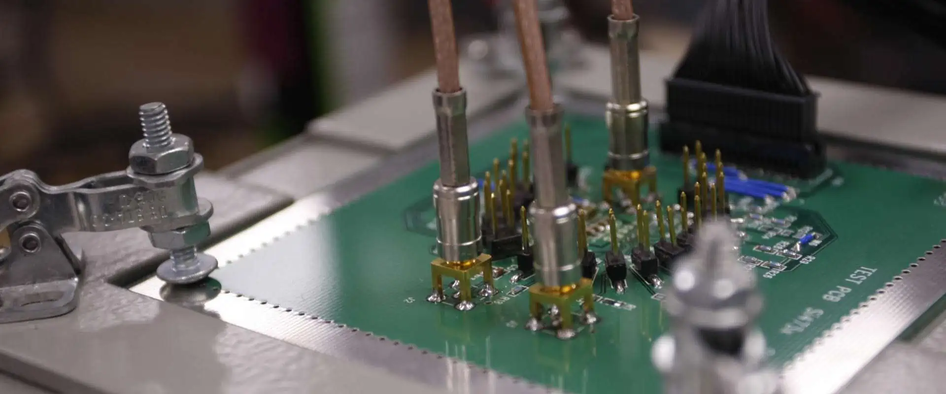
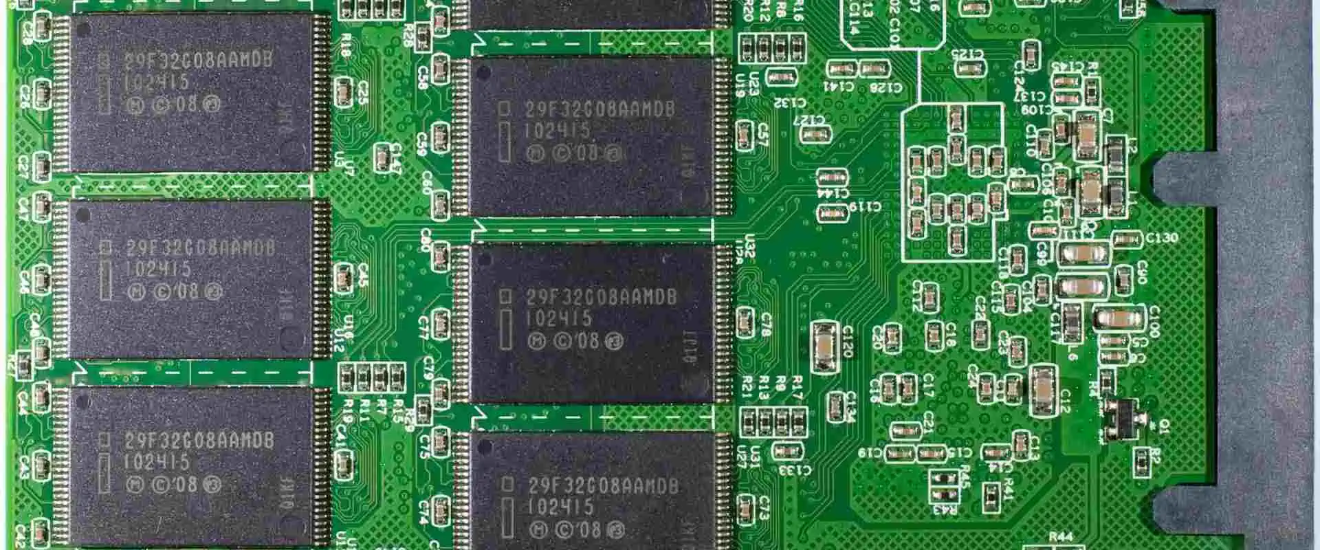
What is a Printed Circuit Board?

Before we move on to discuss the best PCB manufacturer in Vietnam, let us first look at the definition of a printed circuit board:

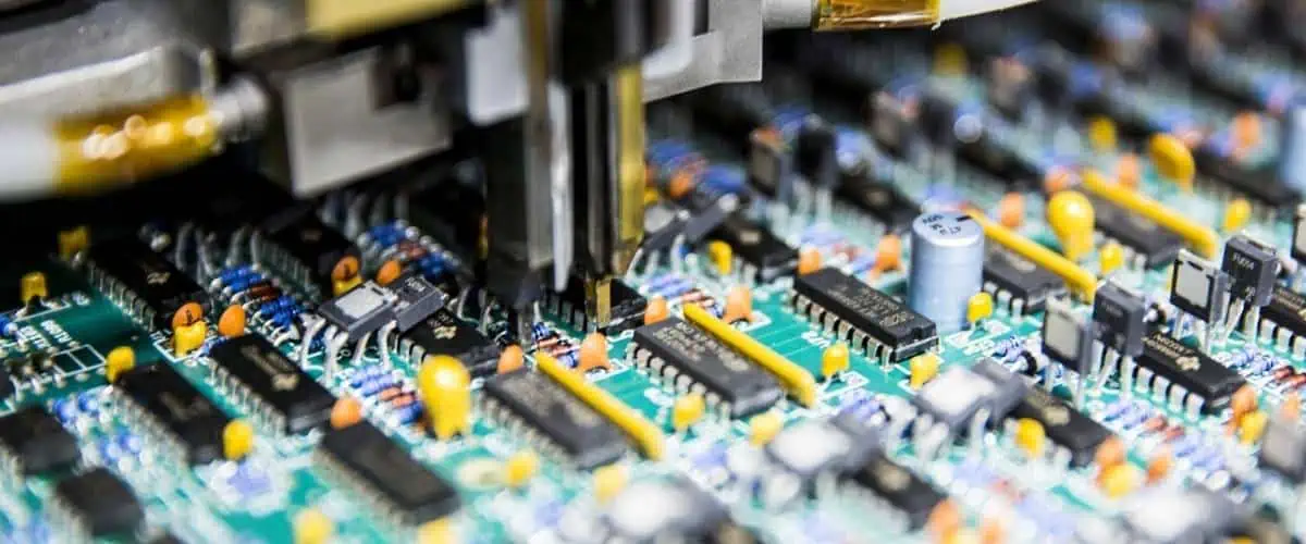
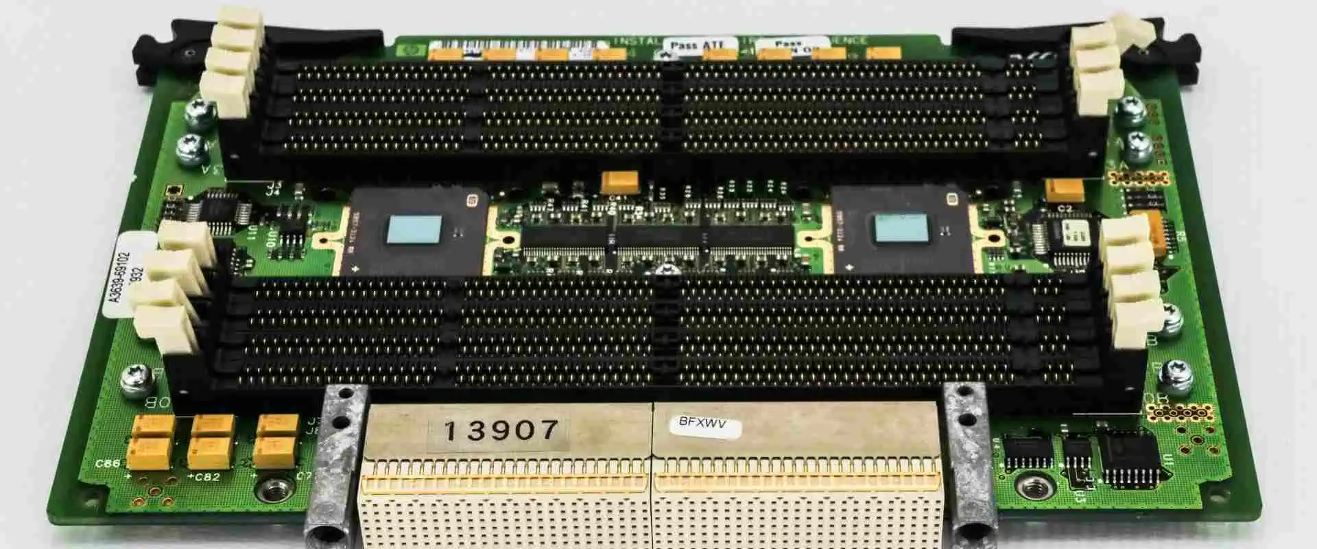
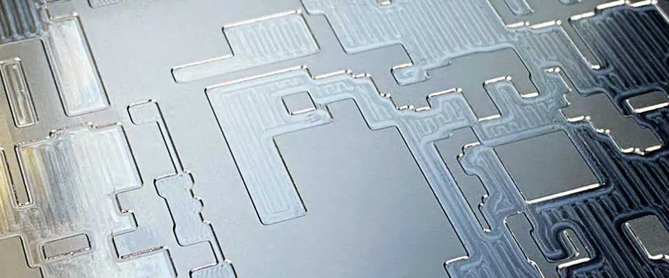
  • Generally, a printed circuit board or a PCB is a thin sheet of insulating components, for example, fiberglass. The insulating parts usually have metallic tracks or circuits etched or printed onto them for efficient electrical conductivity. Most, if not all, modern electronics come with printed circuit boards ranging from mobile phones to tablets, keyboards, laptops, computers, and so much more.

PCB Materials

Typically, different types of PCBs come with varying base materials. The materials the manufacturer chooses to utilize as the base component of a PCB depending on the application area of the PCB. Moreover, the base material must meet several conditions, which include the following:

  • It should be heat resistant
  • It should be durable
  • And lastly, it should be insulating

Some of the most common materials manufacturers utilize to make PCBs include:

  • Ceramic
  • Resin coated copper
  • Epoxy and woven glass
  • Epoxy, cotton paper, and phenolic cotton paper
  • Non-woven epoxy and glass

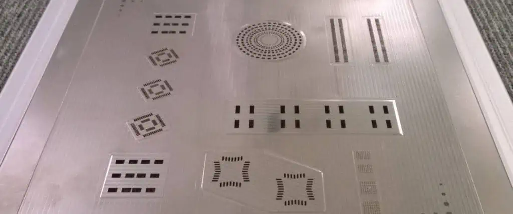
Common types of Printed Circuit Boards

FULL PCB MANUFACTURING Quote

Printed circuit boards come in many different variations, which include the following:

  • Rigid-flex PCBs
  • Flexible PCBs
  • Rigid PCBs
  • Multilayer PCBs
  • Double-sided PCBs
  • Single sided PCBs

The Best PCB Manufacturer in Vietnam

Vietnam has a lot of Printed circuit board manufacturers. Here are the top PCB manufacturers in this country that guarantees high-quality PCBs each time:

Fab 9

Fab 9 is a PCB manufacturing company in Vietnam that hit the market back in 2007. The companyโ€™s headquarter is in Binh Duong Province, Dong An Industrial Park in Vietnam.

Fab 9 offers a “one-stop solution” by catering to all your PCB production needs. Moreover, this company has over fifteen years of experience dealing with PCB production in Silicon Valley and Vietnam.

The goal of Fab 9 is to offer impeccable services and resources to their customers and to generate, launch and sell durable and high-quality printed circuit boards and PCB products.

Main Products

Fab 9 typically handles the following tasks:

  • PCB and PCBA assembly
  • Printed Circuit Boards
  • Box Racks/Build
  • Layout
  • Refurbish

Cicor

pattern expose machine

Cicor is a PCB manufacturing business that focuses on creating a range of printed circuit boards (PCBs). In addition, the company provides various services, including PCB design, manufacture, assembly, and testing. Medical, automotive, computer, communications, and industrial electronics applications are just a few of the ones that Cicor’s products are employed heavily.

The key benefit of Cicor is its capacity to provide a broad range of services to its clients. That comprises PCB design, fabrication, assembly, and testing to guarantee that clients receive the best products that satisfy their needs. Also, Cicor has a strong customer care group that is committed to assisting clients with any problems or inquiries they may have.

The modern production and assembly facilities at Cicor are another benefit. These facilities are furnished with cutting-edge machinery and technologies, enabling the company to create PCBs of excellent quality and dependability. Cicor also employs the most up-to-date manufacturing techniques to guarantee the best possible quality for its products.

The price of Cicor is the sole drawback. Compared to other PCB production companies, the company’s products are rather pricey. Yet, buyers can rest easy knowing their money will be safe because the company’s products are of a high caliber and worth the price.

Generally, Cicor is a reputable PCB manufacturing business that provides a vast array of services and high-quality goods. Customers receive the highest-quality goods tailored to their demands thanks to the company’s cutting-edge production and assembly facilities and skilled customer service staff. Although some of its items can be pricey, their high caliber and dependability make them worthwhile purchases.

Main Products and Business

Typically, Cicor handles the following processes and products:

  • Thick and thin-film substrates
  • Plastic injection molds
  • Tool fabrication and design
  • Box building
  • Test engineering
  • Hybrid circuits
  • Microelectronic assembly
  • PCB assembly
  • PCB

Fujitsu

Fujitsu is a Vietnam-based PCB manufacturing company that hit the market back in 1999. The company’s headquarters is at Me Tri Ward in Tu Liem District, Vietnam.

The company has a long history of generating impeccable experiences and ideas. Moreover, Fujitsu strives to advance its clients and society as a whole. Furthermore, this company drives the success of its clients and promotes a more efficient and sustainable world by combining cutting-edge tech and impeccable integration capabilities.

Fujitsu tries its best to bring cross-industry and high-tech functions to your business focus. Moreover, this company is committed to altering the whole world and making it a place where we can exist in impeccable prosperity via Fujitsu Uvance.

Main Products

Generally, Fujitsu deals in the following products and processes:

  • Pay per use
  • Support
  • Network
  • Infrastructure management
  • Computing products
  • Co-creation
  • Artificial intelligence
  • Internet of things
  • Cyber security
  • Work-life shift
  • Management infrastructure
  • Application and business services
  • Multi-cloud

Jong Gong

nanya-pcb-material

Vietnam-based Jong Gong is a printed circuit board manufacturing business. The business specializes in creating high-quality printed circuit boards (PCBs) for use in various electronics, including consumer electronics, medical devices, and communication systems. Jong Gong offers boards for both mass manufacturing and prototypes. In addition, the company provides a wide range of services, including designing PCB layouts, placing components, and assembling and testing products.

Jong Gong is renowned for its quick lead times and high-quality goods. The business employs cutting-edge technology to create printed circuit boards with precise tolerances. They also use cutting-edge testing methods to ensure the boards satisfy the necessary quality standards. The company produces both single-sided and multilayer boards. Clients can select from several materials, including laminates made of polyimide, FR-4, and copper-clad laminates.

Working with Jong Gong has certain benefits, one of which is their affordable cost. Additionally, the business provides a vast array of customized services to fit consumers’ requirements. Also, the firm provides numerous payment methods and offers discounts for large orders.

If you decide to work with Jong Gong however, you might face a few drawbacks, the biggest one being occasionally sluggish customer-company communication. As the organization is headquartered in Vietnam, it could be challenging to contact the client immediately. Also, as the company does not warrant its goods, clients should always be alert for potential PCB problems.

Overall, Jong Gong is a reputable PCB manufacturing company providing affordable premium goods. However, customers should always be aware of potential communication problems while dealing with the business.

Main Products

Generally, Jong Gong specializes in the following areas:

  • Electronic equipment manufacturing
  • The electronics equipment sales
  • Electronics wholesales
  • Electronics design
  • Audio equipment

Meiko

Meiko is a Vietnam-based printed circuit board manufacturing company established in 2007. The company’s headquarters is in Cam Giang District in Hai Duong, Vietnam.

Generally, this company provides cutting-edge PCB production, for example:

  • Any Layer HDI โ€“ this PCB production allows free connection between various PCB layers. Moreover, this product helps generate PCBs that fit in handheld gadgets such as mobile phones and tablets.

Moreover, this company provides high heat dissipation and high current printed circuit boards that are durable and resistant to various harsh environments, for example, the interior parts of a solar power generator or automobile engine.

Main Products

Meiko mainly deals with the following processes:

  • Imaging system
  • Imaging devices
  • PCB tester
  • Solder stencils
  • Embedded devices PCBs
  • Heat Dissipation printed circuit boards
  • High electric current printed circuit boards
  • Flex-rigid printed circuit boards
  • Flexible printed circuit boards
  • HDI-printed circuit boards

Meritronics

Rogers TC350 PCB

Meritronics hit the market in 1995; since then, it has been a force to reckon. The company is located in Nam Tu Liem District in Hanoi, Vietnam.

 Meritronics offers complete electronic PCB design services which help their clients bring their products to the electronics market fast and efficiently. Moreover, this company has impeccable experience, which gives their clients peace of mind in terms of quality production.

The company major in providing the following services:

Moreover, this company also offers functional test processes, cost reduction designs, product reliability tests, concept, and industrial design rendering, circuit testing, process design, and operational test procedures. Additionally, meritronics also processes clients’ designs to ensure they meet their expectations.

Main Products

Generally, Meritronics deals in the following processes and products:

  • Mold design
  • 3D modeling
  • Mechanical design
  • Printed circuit boards design
  • Firmware and hardware design

SAOKIM

Saokim is a Vietnam-based company that has been around since 2004. The company’s headquarter is in Ho Chi Minh City in, Vietnam. Since the company has been around for some time, it has impeccable experience in terms of handling printed circuit boards and electronics in general.

Typically, this company handles SMT Glued component processing, electronics assembly, and electronic PCB assembly. Moreover, Saokim also majors in PCBA and bulk printed circuit board production, which makes them the perfect choice if your project requires PCBs in bulk.

To generate high-quality and precision printed circuit boards, Saokim utilizes high-quality gadgets and high-tech testing equipment that ensure accuracy each time. Additionally, this company complies with the ISO-9001 2008 standards when producing printed circuit boards which help them maintain their quality PCB production process.

Main Products

Saokim deals in the following processes and products:

  • Circuit board assembly
  • Bulk-printed circuit board production
  • Multilayer printed circuit boards
  • Single-layer printed circuit boards

Sunching

Sunching was established back in 2001 and its headquarter is based in Binh Duong Pro in Vietnam. The company utilizes cutting-edge technology to cater to a pretty wide range of PCB requirements for its clients worldwide. Moreover, the company utilizes most of its resources to offer impeccably high-quality PCB products, guaranteed lead times, and impeccable after-sale services to its clients.

The environmental management program and manufacturing firms of this company are all ISO 14001 and ISO 9001 certified. Moreover, all products that ship from this company meet international UL safety standards.

Sunching is pretty confident in terms of always delivering high-quality products to its clients. However, to achieve this, the firm has to utilize impeccable R&D skills, high-tech gadgets, and extensive experience in the industry. But overall, this is a company that you should try out if you are looking for quality services and products.

Main Products

Generally, Sunching handles the following products and processes:

  • Design development
  • Printed circuit board assembly
  • Multilayer PCBs
  • 1,2 layer printed circuit boards

Vector

Vector or Vector Fabricator is a Vietnam-based PCB manufacturing company that has been in the PCB industry since 1995. The company’s headquarter is in An Town, Binh Duong in, Vietnam.

The establishment of Vector was to help support electronics engineers and the generation of more efficient electronic products. The company knows that PCBs have multiple applications in various industries, which includes the medical and military sectors. Moreover, the company also keeps in mind the fact that the complexity of various PCBs tends to vary according to the application area of the circuit board. Therefore, to cater to various PCB requirements, Vector utilizes cutting-edge tech and highly trained employees. Moreover, this company also constantly trains its employees; consequently, they are always in the know in terms of innovative production processes or changes in the manufacturing process.

Main Products

Generally, this company handles the following products and processes:

  • Micro-BGA, BGA, SMT and fine pitch
  • Multilayer, double-sided, and single-sided printed circuit boards
  • Buried and blind vias
  • Burn-in and load boards
  • Quick turn prototypes

Vexos

multilayer pcb manufacturing

Vexos is another famous PCB manufacturing company that is based in Vietnam. Although the company hit the market back in 2019, it has been growing pretty fast. The headquarters of this company is in Ho Chi Minh City in, Vietnam.

Vexos offers mid-to-low volume, high complexity, high mix, and complete service electronics manufacturing. Moreover, this company also provides custom material solutions. Therefore if your PCBs need extra customization, this company might help you.

Vexos is committed to providing high-quality products. Actually, this commitment has seen Vexos work with various groups of manufacturers that generate original electronic gadgets.

Main Products

Generally, Vexos handles the following processes and products:

  • Third-party logistics
  • Custom tooling
  • Component obsolescence management
  • Prototype PCBs
  • Custom component solutions
  • Full Box Builds
  • DFT/DFM
  • Printed circuit boards assembly
  • NPI
  • EMS Services
  • Electro-mechanical Components
  • Harness and cable Assembly Services
  • Metal Fabrication
  • PCB solutions

Unigen

Unigen is among the oldest Vietnam-based PCB manufacturing companies since it was established in 1991. The company’s headquarters are in Tu Son Township, Bac Ninh Province, in Vietnam.

Since Unigen hit the market, it has grown to become a global leader in the production and design of bespoke and original solutions for flash and DRAM storage. Moreover, this company has multiple manufacturing firms spread out across the world, which include:

  • A manufacturing firm in Silicon Valley which is IO 13485/14001/9001 certified
  • A manufacturing firm in Hanoi that is ISO 14001/9001 certified

Moreover, this company sells its electronics products to multiple OEMs worldwide in the medical, automotive, imaging, telecommunication, server, industrial, and embedded devices industries. Additionally, Unigen offers impeccable EMS (electronics manufacturing services), for example:

  • Intro of volume and new products
  • Supply chain management
  • Post-sales support
  • Testing
  • Assembly

Main Products

Unigen mainly handles the following processes and products:

  • PI and SI test results
  • Stack-up drawing printed circuit boards
  • Assembly drawing
  • Board bring-up instructions
  • Design for Manufacturing
  • Printed circuit boards fabrication package

Trung Nam EMS

Trung Nam EMS is among the more recent Vietnam-based printed circuit board manufacturing companies that hit the market in 2020. The Trung Nam EMS Vietnam base is located in Hoa Vang District, Danang City.

Although Trung Nam EMS hasn’t been around for a while, it has become pretty popular due to its utilization of high-tech gadgets to gain impeccable precision. Moreover, this company also offers various manufacturers worldwide impeccable assembly designs and electronic components.

Main Products

Trung Nam EMS mainly offers the following product and processes:

  • Rigid-flex and flex PCB designs
  • Burn-in and tests
  • Electronics prototypes
  • Box build/system
  • Logistics and supply chain
  • Printed circuit board assembly
  • PCB engineering and design

Conclusion

Printed circuit boards are, without a doubt, crucial components in most, if not all, electronic gadgets. However, these components also need complex processes to generate. Luckily there are multiple manufacturers spread out across the world that offer PCB production services. Unfortunately, however, not all PCB manufacturers provide high-quality services and products. Therefore we hope this article will help you find the right match if you are looking for a PCB manufacturer in Vietnam.

Understanding What Populated PCB Is All About?

Consumer Electronics Assembly

Being aware of the variety of Circuit boards is crucial for engineers. An essential component of the Circuit board industry is populated PCB. A PCB would just be a naked board without it. Professionals handle this part to prevent any errors.

The populated PCB affects a circuit board’s operation and performance. It is essential to comprehend what the PCB populace consists of. We will go over significant information about the populated PCB in this essay.

YouTube video

What Does a Populated PCB Mean?

Any circuit board having electronic components is called populated PCB. are boards are one that doesn’t have any installed electronic components on it. A PCB may therefore be either populated or bare. PCBs could be filled using through hole or the surface mount method.

A PCB assembly is identical to a populated pcb. These board’s components are surface-mount devices. Electrical equipment which links electronic components is known as Populated PCB. This PCB has conductive tracks, pads, and other features.

To create the populated PCB, manufacturers help in soldering electronic components onto the board. IC, diodes, and capacitors are some of the components on the populated PCB. The bare board lacks electronic components, but populated PCB does.

It’s critical to recognize the distinction between the populated PCB as well as PCB fabrication. The creation of the bare board is a step in the PCB manufacturing process. A circuit board prototype is made throughout the production process. The way a PCB is filled is dependent on a circuit board’s intended use.

What are the Tips for a Populated PCB?

An aspect which involves some processes includes PCB population. While populating the board, the planning, the organizing as well as sorting are highly crucial.

Sanitize the bare PCB

The process of filling the circuit board starts with this. So clean the board to get a populated PCB that works. You should clean the PCB prior to and following filling it. You can successfully execute soldering by cleaning your Board.

Fill PCBs starting at the lowest level and working your way up

If you’re not careful, PCBs could get overpopulated. Your situation is made more challenging by the overpopulated PCB. It gives you very little room to mount your components where they need to be. Planning ahead is the preferred approach to stop overpopulation from happening. Connect your components using solder throughout the bare boards.

Start by placing the cheapest component on the board. By doing this, large objects won’t get in the way.

Use tweezers

Tweezers are required for through-hole mounting. You can put the thru-hole components on top of your circuit board with the aid of tweezers.

Use a tool for component leads.

The tool for component leads bends lead components of all sizes and shapes while measuring hole spacing. Use this tool for maintaining the stability of your circuits. It can be useful to bend the component leads onto the proper lead width.

Use poster putty to create helpful hands.

Among the populated PCB, poster putty serves as a underutilized tool. While working on little objects, this tool could assist in holding them. In place of traditional extra hands tools, poster putty may be utilized. This tool will not leave behind any traces on the PCB whenever it is used.

Insulation made using hot glue

Hot glue could serve as a barrier when attaching components on Boards. Hot glue shouldn’t be used to components that are thermally sensitive, though. You can secure cables in the proper location with hot glue.

Plan your enclosure

In the process of populating the PCB board, this is crucial. A circuit board’s size and shape are constrained by enclosures. Choose an enclosure which satisfies the demands of the planned use.

Do not handle or reposition as much

Circuit boards need to be moved around more often, which extends the time needed for the population of the PCB. When the board becomes two-sided and there are components present on both sides of a PCB, repositioning is necessary. Using all the components of the SMT on one side of your board is advised.

Methods for Population of PCBs

FULL PCB MANUFACTURING Quote

Manufacturers employ two main methods for creating the populated PCB. These methods include through-hole and surface-mount. A PCB can be populated using THT and SMT.

SMT

This can be described as a typical method of populated PCB. Manufacturers mount delicate components using SMT. The components in the SMT have short leads. Moreover, this method populates components on the circuit boards using automated machinery. Direct SMD mounting on the Circuit board is known as SMT. Manufacturers utilize pick & place machines to populate the circuit board.

THT

The pins for the components are inserted into the board’s holes using the thru-hole method. Here, the component placement must follow the guidelines of the through hole process. This method is used by manufacturers to position a component onto circuit boards.

Manufacturers, however, insert components containing leads through plated thru holes in THT. Before the invention of SMT, this method of filling boards was widely used.

Factors Affecting the Populated PCB

While populating the bare board, manufacturers need take a few things into consideration. Several elements have a direct impact on the populated PCB process.

Portion size

The size of the electronic parts on circuit boards varies. The size of the components must be taken into account by the manufacturer when choosing the process speed. The device for pick and place will adjust for part size.

Speed of placement

The process of populating the PCB entails attaching components to bare circuit boards. There are many processes involved in this aspect.

Reducing the amount of processes will speed up placement for manufacturers. For instance, if components are pointing in the same direction, you can position them without rotating them.

Board types

PCBs come in a variety of forms. How and where to populate it will depend on the type of board. Multilayer board types will have a different population than the single layer boards.

Advantages of Populated PCB

A filled PCB comes with many benefits. It is crucial to understand that populated PCBs are what are employed in the production of electronics. In the absence of electronic components, the bare PCB is inoperable. In our electronics world today, populated PCBs are crucial.

Compact design

Putting electronic parts on the circuit board results in a small and compact design. Thus a Circuit board designer can try to create a fantastic design when filling a PCB. Connecting the components coupled with enabling input and output connections are populated PCBs.

Great option

For many businesses, a populated PCB is a dependable choice. It is a dependable alternative that may be used in a variety of products. These boards are durable. Manufacturers fill a board according to a predetermined pattern. This enhances the consistency of these boards.

Inaudible electrical noise

In circuits, electronic noise could easily happen. The components are mounted by the manufacturer to minimize the electronic noise generated by this circuit. Path lengths can be shortened by populated PCBs to cut down on electromagnetic emission.

Repair is simple

Every board flaw can easily be tested for and found. As a result, producers can quickly spot a defective component then replace it. This can be done without affecting other electronic parts of the circuit board.

What are the Applications of Populated PCB?

High-Volume-PCB-Production-and-Assembly

 An extensive range of different applications frequently make use of populated PCBs. There are versions of this board for most modern gadgets.

Military

In military equipment, populated PCB is frequently employed. The increased demands of our military industry are being met by these boards. In military equipment like the machines for missile detection, populated PCBs are found. Nonetheless, producers create populated PCBs of high frequency ffor use in the military.

Consumer Electronics

Electronics like TVs and remote controls work with the populated PCB. The core of such devices are these types of circuit boards. They provide these devices with mechanical as well as electrical support. Connected boards that have been populated aidS in the creation of laptops and Cellphones.

Medical industry

There is yet another use for populated boards. There are more and more populated PCBs being used in the medical sector. These circuit boards are excellent for tracking diagnosis, therapy, and other procedures. These boards can also be found in ultrasound, CAT, as well as other medical equipment.

Aerospace

Populated PCBs are also used in the aircraft sector. Inside this application, high-speed as well as high-frequency boards are used. They seem to be more susceptible to challenging circumstances, which explains why. This PCB is used in aerospace technologies like satellites, aircrafts, and radio communication system.

Populated PCBs work well in a variety of applications. They are excellent in every way, making them suited for the majority of applications.

Conclusion

The electronics industry places a high value on populated PCB. This board has several uses and is widely employed. The majority of electrical devices rely on them as their core. The populated PCB is produced in large part by the PCB population. This procedure needs to be followed attentively. Technology advancements have made PCB population simpler.

Features, Applications, and Components of the Arduino UNO PCB

Arduino UNO PCB

There are several open-source platforms for developing electronics projects. Arduino is one of such platforms. It is specially designed for creating and developing several electronics projects. Comprising a physical programmable circuit, and Integrated Development Environment, the Arduino can be used in uploading and writing computer code to a physical board. The physical programmable circuit board of Arduino is known as the microcontroller while the integrated development environment is the software.

Over time, the Arduino board has gained popularity among people who just started developing electronics. This is because Arduino is different from other programmable circuit boards developed in the past. Unlike those boards, Arduino requires no programmer to load a new code. All you just need is a USB cable and you are good to go. Asides this, Arduino offers several features and benefits.

Arduino features various boards. The Arduino UNO PCB belongs to the Arduino family. To explore the Arduino UNO PCB, you need to understand how it functions, its features and how to integrate it in your electronic project.

YouTube video

What is Arduino UNO PCB?

Arduino UNO board

The Arduino UNO PCB comprises a physical programmable circuit and a piece of software. As a microcontroller, this board integrates the ATmega328. The Arduino board is a popular board which belongs to the Arduino family. It is a user-friendly board for beginners as it helps them build their electronic projects with much ease. Due to the features of this board, it is the most popular of all the Arduino boards.

Arduino UNO PCB comes with a lot of components which include 14 digital input/output pins, a USB connector, ICSP header, a power jack, and a reset button among others. These components are crucial in ensuring the functioning of the Arduino UNO PCB. Also, a USB port is used in charging this board. However, you can charge the Arduino board with its DC supply.

Components of the Arduino UNO PCB

As earlier mentioned, Arduino UNO PCB features various components which play crucial roles in its functioning.  Arduino boards are available in various types. However, these components are common in Arduino boards.

USB Port

All Arduino boards feature a USB. There is a need to connect these boards to a power source. Therefore, the USB cable from a computer can power the Arduino UNO PCB. Also, this board can be powered by a power supply in a barrel jack. Arduino UNO PCB comes with a barrel jack and a USB connection cable. Another function of the USB connection is that it enables users to load code on the board.

Reset button

The Arduino UNO PCB features a reset button. If you intend to connect the reset pin to ground, you just need to push the button and then restart code loaded on the board.

Main IC

The main integrated circuit of the Arduino UNO board looks like metal legs. This component is the brain of the Arduino UNO board. In Arduino boards, the main IC differs. The main IC of the Arduino UNO PCB is different from another Arduino board. However, the main IC of the Arduino boards always comes from the ATmega line.

It is important to know the type of IC before you load a new program. The details of the main IC are usually written on the ICโ€™s top side.

Power LED indicator

FULL PCB MANUFACTURING Quote

The Arduino UNO PCB features a LED which lights up anytime the board is plugged to a power source. The LED is just beneath the word โ€œUNOโ€ on your UNO PCB. If the LED on the Arduino UNO board fails to come on, something might be wrong. This can help you easily detect any problem with your board.

Voltage regulator

Another important component on the Arduino UNO PCB is the voltage regulator. This component regulates the amount of voltage that passes into the board. It is like a gatekeeper that rejects any extra voltage to your board. This extra voltage might be harmful to your circuit board. The Arduino UNO PCB has its voltage limit. Avoid connecting this board to a device with more than 20 volts.

TX RX LEDs

RX simply means receive while TX means transmit. The TX RX markings indicate the pins for serial communication. In the Arduino UNO PCB, you can see the TX and RX in two places. You will see it next to the TX and RX indicator LEDs. With these LEDs, users can know when the board is transmitting or receiving data. Therefore, the TX RX LEDs is a good indicator.

Pins

Every Arduino board comes with pins. However, the number of pins may differ according to the types of board. The pins provide space for connecting wires to develop a circuit. These pins feature plastic headers that enable users to plug a wire right in the board. There are different types of pins on the Arduino UNO PCB. Each of these pins is labeled. These pins serve various functions.

Crystal Oscillator or Ceramic Resonator

A microcontroller like the Arduino board requires a clock source. The operation of the microcontroller depends on the clock circuit. Also, the clock frequency determines the instructions per second a microcontroller will carry out. The ATmega series is usually integrated in Arduino boards. These microcontrollers can integrate two different clock sources.

Arduino UNO PCB Pins

Arduino Python Projects

The Arduino UNO PCB has various types of pins. Each of these pins has its own functions. Also, it is crucial in the functioning of the Arduino board. Here, weโ€™ll be discussing the various pin types on the Arduino UNO PCB.

Analog pins

Arduino UNO PCB comes with six analog pins. These pins are labeled A0 to A5 on the board. Analog pins are capable of reading the signal coming from an analog sensor. For instance, they can read temperature and convert to a digital value.

AREF

AREF refers to Analog Reference. The AREF pin is usually integrated in setting an external reference voltage.

GND

GND is the short form of ground. The Arduino UNO PCB comes with several ground pins. Users can integrate any of these pins to ground their circuit.

Digital

The Arduino UNO board comes with several digital pins. These pins can tell if a button has been pushed. They are ideal for both digital output and digital input.

5V and 3.3V

The 5V pin supplies volts to the board. Basically, it supplies 5 volts of power. On the other hand, the 3.3V pin provides 3.3 volts. The majority of simple components integrated with Arduino run on either 3.3 volts or 5 volts.

PWM

The PWM pins function like normal digital pins. PWM stands for pulse width modulation. However, you can also use it for a Pulse-Width  Modulation.

Importance of Arduino UNO PCB

The Arduino PCB is an ideal option for beginners. As a newbie in the development of electronic project, the Arduino UNO PCB will help you have an enjoyable experience. The UNO board comes with an innovation which makes it ideal for electronics projects. Also, the Arduino UNO PCB is the most popular board among the Arduino boards. Well, this board is preferable because of the following benefits.

Enables connection to other computer system

You can use the USB port in the Arduino UNO PCB to connect to other computer systems. The functions of the USB port involves supply of power to the PCB and can serve as a serial device to link the board.

Flexible microcontroller

Arduino UNO PCB features the ATmega328 which offers a great level of flexibility. This means users can easily replace the controller chip and remove it from the board if there is any damage. Other Arduino boards donโ€™t have this flexibility.

Great power supply

The pins of this board provide great power supply. Also, the Arduino UNO PCB can get power from a direct current (DC) adaptor with a voltage of 12V. You can charge this board from an external power supply.

Simple board design

Another benefit of using the Arduino UNO board is its board design. The design of the board makes it easy for multiple users to use. Also, this board offers community support for users.

Low cost

This is an added advantage. The Arduino UNO PCB goes for a very low price. Its price is lower than most Arduino boards. Therefore, it is a go-to-option for engineers and developers.

Enables interaction with other devices

The Arduino UNO board features several components and can communicate with other hardware devices like motor control, Bluetooth, and more.

Features of Arduino UNO PCB

Arduino UNO PCB is equipped with a wide range of features needed to run the controller. This board offers the following features:

Quick start

The board has a reset pin that helps you reset the whole circuit board. Also, the reset pin comes in handy when the board stops working when running the program. All you need to do is push this pin and everything in the program will be cleared. After this, it will help you start the program from scratch.

Low voltage requirement

This board needs 5V to get turned on. Users can achieve this by integrating the USB port directly. However, the Arduino UNO board can offer support to external power source of about 12V. This volt can be limited to 3.3V or 5V according to the projectโ€™s requirement.

USB interface

This board features a USB interface. With this feature, you can develop a serial communication with other devices.

More number of instructions per cycle

The UNO board integrates the Atmega328  microcontroller. This microcontroller is equipped with features such as PWM, I/O pins, timers, and interrupts.

Greater flash memory

This board features a flash memory of 13KB which helps in storing instructions in form of code.

More storage

Arduino UNO PCB offers support for Micro SD card to help store more data.

Power alternatives

There are other power alternatives aside from the USB. Arduino allows users to use AC adapter or battery to power the board.

Plug and Play

This board requires no fast interface to link devices. Users need to plug the external device to the boardโ€™s pins.

Real-time Applications of Arduino UNO PCB

Arduino Uno PCB is suitable for use in several applications. Engineers and developers are integrating the Arduino UNO PCB for developing instruments and sensors used in scientific research.

The integration of Arduino UNO in developing some projects applications enhanced its use in several  IoT projects.

Below are some real-time applications of Arduino UNO:

Home Automation System

The home automation system is an IoT project that can be developed with the Arduino uno board. This board develops the system with Bluetooth. With Houses becoming smarter, more people are integrating the Arduino board to achieve home automation. Also, modern houses are now using remote controlled switches, hence, there is a gradual shift in the way of design.

Auto Intensity Control of Street Lights

It isn’t possible to install High Intensity Discharge (HID) lamps on street lights since you can’t control the intensity of this light. The Arduino UNO PCB helps in developing auto intensity street lights.

Plant Watering System

The Arduino UNO PCB is a great option for developing the plant watering system project. This system integrates a soil moisture sensor and waters plants based on the soil moisture level.

Other Applications of the Arduino UNO includes:

  • Security and defense
  • Embedded System
  • Digital Electronics and Robotics
  • Weighing machines
  • Parking Lot Counter
  • Medical instrument
  • Traffic Light Count Down Timer
  • Home Automation
  • Industrial Automation
  • Emergency Light for Railways

Conclusion

Arduino UNO PCB is a low cost microcontroller that comes with advanced features. Unlike other microcontrollers, its software runs in OS, windows, Mac, Linux. The Arduino UNO board is a good platform for the development of pilot projects and innovation of new technologies. This board features various components which play crucial roles in its functioning.  

It is a user-friendly board for beginners as it helps them build their electronic projects with much ease. Due to the features of this board, it is the most popular of all the Arduino boards. As a newbie in the development of electronic project, the Arduino UNO PCB will help you have an enjoyable experience.

What is Carrier PCB and Why is it Useful?

Carrier PCB

The internet’s carrier PCBs, which convey massive amounts of data, are its structural foundation. The majority of internet-served data must travel via many carrier networks before reaching the requester.

Some carrier networks may agree to forgo the fee to help their favored partners or they might be required to pay to send data to some other networks.

YouTube video

What Does Carrier Network Mean?

A carrier network for communications is a group of hardware and supporting infrastructure that is used to send information from one place to another. This service for data transmission is offered as commodity and can be purchased through a reseller or directly from an end user.

Computers as well as other gadgets need to be connected for internet to operate. For instance, the physical path from TechTarget servers towards the device of the user is required for a Smartphone or desktop computer to display this webpage. It is obvious that it is impractical to connect them with one long cable.

This equipment used to transport information from one place to another as well as connect various carrier networks is owned and maintained by several carriers. Moreover, an internet service provider may occasionally be the owners of such carrier networks as well as offer services to the end customers.

For instance, when you purchase anything online, this store often is not in charge of shipment delivery. It uses a number of providers to deliver the package out from warehouses to your door step, including US Postal Service, FedEx, or UPS.

The same holds true for data and phone services on mobile devices. It’s possible that the networking hardware used to transport calls or texts to their intended locations may not belong to the original carrier network, the person’s provider.

What Does a Carrier PCB Mean?

Carrier circuit board

Data carrier circuit boards are in charge of transmitting massive amounts of data and are the foundation of the web. The majority of internet-served data must travel via many carrier networks before reaching the requester. Some carrier networks might well have agreements that waives the fee to please their favored partners or they might charge a little fee to send data to the other networks.

In the telecommunications system, the carrier PCB gets integrated into its carrier system. By modulating one or more carrier signals well above the primary voice frequency as well as data rate, this carrier PCB aids its carrier system in transmitting information, including a phone conversation’s voice signal and a television’s video signals.

Using various multiplexing techniques, carrier PCB often transmits numerous communication channels simultaneously across a shared media. Time-division multiplexing as well as frequency-division multiplexing are two common techniques for multiplexing the carrier signals. Frequency-division multiplexing is used, for instance, in cable television systems. This coaxial cable can transmit multiple television programs all at once, each at separate frequencies. A specific input signal may potentially undergo numerous levels of multiplexing.

For instance, time-division multiplexing is employed by publicly switched telephone networks to send a large number of calls through shared trunk line. Frequency-division multiplexing can be used to send a number of such channels through a satellite link for communication for the long-distance calls. Channels can be individually demultiplexed at a specific receiving node.

How Does Carrier PCB Technology Work?

FULL PCB MANUFACTURING Quote

Every phone number serves as both the signal’s destination and a collection of instructions concerning how a call must be routed between both the caller as well as the recipient along the switching stations. At the national, local, and international levels, calls are forwarded through numerous switches.

When telephone networks were first widely used, switchboards as well as operators had to physically link calls via separate copper wires and cables.

During late 1980s, this technique had all but disappeared, and calls had started to be converted to digital form. This made automatic switching possible and also allowed for a lot more calls to be placed on each line.

Fiber-optic technology has made it possible for numerous calls to travel down the same connection more recently. Internal calls at offices are forwarded via private branch exchanges. This is effectively a switch station that the business manages, enabling it to assign phone numbers as well as make free internal calls.

The PBX is connected towards the carrier as well as the larger phone network through a trunk connection.

Analyzing Carrier PCB Diversity

You should discover every detail you can about the real physical circuit routings before installing alternative WAN links. The backup path may be prone to similar failures like the primary path since other carriers occasionally use this same facilities. If you want to be confident that the backup is indeed a backup, you need conduct some research. The ideal configuration of circuits employing several pathways is referred to as circuit diversity by network experts.

It is becoming more difficult to ensure circuit diversity since carriers loan capacity to one another and utilize third parties which provide capacity to numerous carriers. Moreover, carriers frequently combine with one another, mixing their circuits thereafter. Planning variety becomes considerably more challenging as carriers adopt automated ways for the rerouting of the physical circuits. This is due to the fact that rerouting is known to be dynamic.

This circuit diversity level in the network design should be understood by working with the suppliers of the WAN connectivity. In most cases, carriers are open to working with clients to offer details on physical routing of the circuit. (But, keep in mind that carriers occasionally present incorrect data depending on databases which aren’t kept up to date.) Contracts with the providers should attempt to include promises to the circuit diversity.

Make sure to examine the local cabling as well as the services of your carrier while examining circuit diversity. Maybe you created the ISDN link as a backup for Frame Relay links. Do all of those links utilize identical cabling to reach the building network’s demarcation point?

How are the links connected to the carrier? What kind of cabling? The network’s weakest link is frequently the cable that connects a building to a carrier. Construction, ice storms, flooding, can have an impact.

Importance of Carrier PCB In Telecommunication

FT1 BGA Assembly

Modern life would not be possible without telecommunications, which allow us to text, call, email, as well as connect to the internet. The carrier PCB serves as a crucial component of such a system since it offers the mechanical support and electrical connection required for telecommunications.

A carrier takes charge of running networks, moving data, and making sure users can access services. Additionally, it facilitates dependable communication between users, enabling them to use services like voice, data, and text.

Understanding the function of the carrier PCB would be crucial to comprehending how well the telecom carrier system functions.

Carrier Technology in Telecommunications

Users may send as well as receive data across great distances thanks to carrier technology, that is today a crucial part of the telecommunications systems. This infrastructure supporting data transmission is provided by a carrier, commonly referred to as the telecommunications carrier. The group comprises, among others, traditional phone providers, wireless service providers, cable providers, as well as providers of internet services.

By making infrastructure investments, carriers may offer a variety of services for their consumers, such as voice, video, and data. Users may interact with each other, use the web, or stream media from all over the world thanks to carrier PCB technology. A stronger sensation of separation from the outside world is made possible through carriers.

Function of Carrier Networks in Cellphone

Mobile devices need a network so as to function. The carrier PCB network owns the base stations as well as interconnections for radio equipment utilized for data transmission as well as radio spectrum utilized by these serviced phones.

These main cellular service companies are in charge of maintaining the network infrastructure and radio airwaves, and they offer service to customers directly. These businesses are identified as mobile telecom companies and may also be called wireless carriers, cellphone providers, or providers of mobile services.

Some types of cellular service providers just resell the services of big providers and lack the necessary equipment. They are known as Mobile Virtual Network Operators or just, service provider since they utilize the network of another company as a carrier network providing their service.

The robustness of any underlying carrier networks is increasingly crucial as cellular data demand grows. The most recent performance standard for cellular technology, 5G-NR, offers wireless broadband routers and handsets a faster speed than the 4G LTE network now in use. To enable this growth, more wireless spectrum and quicker backbone connections towards the wireless stations are needed. Slow connections as well as network congestion are going to be the outcome when cellular networks don’t really expand their capacity to handle the rising demand.

Conclusion

Typically, the carrier PCB function is to either transmit data as electromagnetic waves through space (like radio communication) and to enable frequency division multiplexing, which enables multiple carriers operating at various frequencies to utilize one physical transmission medium.

What is Flux Capacitor PCB โ€“ Back to the Future

Flux Capacitor

In addition to the capacitor on the Board, separate capacitors may also be included. This may work as a group of bundled capacitors. This is appropriate since it may be used to build a distribution system for your premium design.

PCBs have a similar purpose as capacitors. This is due to the possibility that capacitors might be built of two metal objects that are held apart by a non-dielectric substance. So, a capacitor that may disrupt frequency oscillation should be created by mixing PCB components, connectors, pads, and tracks.

Apart from that, grand planes and power provide the required decoupling capacitance. Even the edges of the PCB can be used as capacitors. Only two excellent copper planes are required. These would act as capacitors. After that, we may proceed to couple discrete capacitors with the PCBs capacitor. This could perform similarly to lumped capacitors, something you’ll use to build a distribution network for your design.

YouTube video

Flux Capacitor PCB Contain Layers Too

Flux Capacitor PCB
Flux Capacitor PCB

We frequently employ capacitors that are different from those constructed in a student’s classroom while designing PCBs. You must be aware of the various characteristics of the different kinds of capacitors before designing the PCB. This will support both the planning and the design processes.

You may select capacitors utilizing the design libraries if you’re dealing with through-hole and surface-mounted designs. This decision is made on the basis of many characteristics, including capacitance, temperature coefficient, dielectric type, nominal value tolerance, and rated voltage.

The surface-mounted technique has displaced through-hole installation as the more common mounting method. Yet, for some particular applications, drilling holes and anchoring component leads axially or radially via the board will be beneficial. Anytime components are put under mechanical and environmental stress, dependability is required for industrial, military, and aeronautical applications. The several THM capacitor types include tantalum-coupled ceramic discs, silver mica, plastic film, and polarized electrolytic kinds.

Surface mount (SMT) capacitors are devoid of layer-through hole drilling. Moreover, they will immediately mount to the PCB’s surface. The vials take the role of through-hole wires, allowing a conducting link to be made between the layers of the circuit boards. The Surface-Mounted Technique capacitors are mounted on the board’s each side. Comparatively speaking to through-hole mounting capacitors, they likewise feature compact packaging. Multilayer ceramic, mica, tantalum, film capacitors, and electrolytic, are some of the varieties of SMT capacitors.

How Do Flux Capacitor PCB Work?

FULL PCB MANUFACTURING Quote

Circuits often use capacitors, which are widely recognized passive parts. They are a lot like resistors. An electrical charge may be stored by capacitors. They provide many choices as well. The circuit design is what determines this. The amount of energy or charge that a capacitor can store is determined by its capacitance.

Capacitors are typically composed of two sheets including an insulator sandwiched in between. The dielectric material is this insulator. There are several types of capacitors. They may serve a number of functions and are made of various dielectric materials.

Farads are used to measure capacitance. This particular device is rather big. It is typically utilized in picofarads or microfarads because of this. Furthermore, capacitors can be electrolytic or non-electrolytic. The circuit allows for any potential direction of connection for the former. You must correctly position the electrolytic capacitors when mounting them on the circuit. Only one of them is a positive wire, whereas the other one is negative. It’s possible that the placement of such electrolytic capacitors will prevent your circuits from working properly. They could even pop as a result.

There are several uses for capacitors. Digital electronics play one of their crucial responsibilities. The microchips are shielded from the noise here. They are frequently used with circuit devices and capacitive sensing in flashes and lasers because they can rapidly discharge the entire charge they contain. Capacitor-equipped circuits frequently exhibit frequency-dependent behavior. They can be used on circuits that amplify some frequencies because of this.

Like resistors, you may add capacitors in series or parallel. The computation, though, is exactly the reverse of what was done for the resistors. Components connected in series have the same node. Also, whenever the connection is made in parallel, both nodes are shared. If you wish to find the resistance’s total value, sum the resistors that are linked in series. If you require the capacitance’s entire value, you must also include capacitors that are connected in parallel.

Selecting Flux Capacitor PCB Components For Your PCB Design

In this part, we’ll walk you through the factors you should take into account when choosing electronic components for your PCB, like capacitors.

It will always be difficult for new PCB designers to select the appropriate electronic components. The inappropriate component selection might result in the PCB malfunctioning, failing completely, or operating undesirably.

While picking an electronic component during the stage of design, PCB designers need to take into account a number of crucial factors depending on the type of component. You will learn about key factors to take into account while selecting the primary electronic components in this part.

How To Choose Flux Capacitor PCB?

Many circuits make use of capacitors. Across the majority of instances, selecting the capacitor component for the PCB design employing simply the capacitance value is frequently insufficient. The components in capacitors have tolerance factors much like those in resistors. The actual capacitance of a capacitor component varies. This is determined by the manufacturing procedure, DC biasing, operating temperature, and aging.

Consequently, while selecting the electrical component for the capacitor, the capacitance tolerances must be taken into account. Moreover, there is a sizable price difference between capacitors with both low and high tolerance. However, if cost is not a concern for you, we suggest that you select a capacitor with a tolerance of less than 10%. It is adequate to have a tolerance of 10% or 20% for nearly all low-power circuits.

What Value Of Capacitance Will You Get with Flux Capacitor PCB?

If the voltage is stressed or is greater than planned, your capacitor might be damaged. Capacitors are often wired in series with a subcircuit, an output, or another circuit. Your capacitor’s anticipated voltage loss should be estimated or known. We advise that the voltage buffer ought to be 50% more than the anticipated voltage loss. This implies that if you anticipate a 10-volt reduction in voltage over the PCB capacitor, you should select a capacitor with a 15-volt or higher rated voltage.

The duration during which the capacitor is in good condition and provides capacitance in accordance with its intended use is known as its lifetime or capacitor life. It is obvious how important this is, particularly for the electrolytic capacitor. The maker of a product will typically include the lifespan of a capacitor under normal operating circumstances on the product’s datasheet.

The operating temperatures vary for the capacitor. This needs to be seen similarly to resistors. For advanced designs, it is necessary to consider the operating frequency according to the application kind, ripple power, and ECR value.

Conclusion

Be aware that decoupling provides a store of energy that may be used to assist smooth out voltage if there is a variation in the quantity of current drawn. Because of inductance, it is typical for the power supply to wait a little while before responding to the value of voltage. The decoupling cap must thus close this gap. Ensure that it is closer to the electronic chip in order to do this. Otherwise, the lead’s inductance might cause problems rapidly and make it difficult to obtain extra current quickly.

Top Differences Between An HDI Board & An Ordinary PCB

hdi pcb design

The HDI board, made for low-volume customers, is a compact board with a critical distinguishing feature of high wiring density compared to standard printed circuit boards. This difference between the two types of boards is mainly manifested in the given four aspects. 

HDI PCB 1-step &  2-step, &  3-step

The initial step is pretty straightforward, with easily manageable procedures. However, the subsequent 2-step process becomes more intricate and presents several challenges, including counterpoint, perforation, and copper plating issues. Numerous two-step layouts exist, such as staggered positioning of each layer. This design allows connecting the adjacent coating to the intermediate layer via a wire equal to 2 first-order High-Density Interconnects (HDIs). 

The second point is that 1st order vias intersect, resulting in a second-order effect achieved through superposition. Although the process is identical to first-order vias, several technical considerations require special attention, as discussed earlier. 

The third step involves drilling from an outer coating to the 3rd coating or even the n-2 coating, which is a more challenging process than the previous steps due to the complexity of the hole. A similar approach can be analogized to the 3rd order. 

YouTube video

Differences between HDI board & ordinary PCB

HDI PCB Board Laminate Structure-Blind and Buried vias-3

The commonly printed circuit board is made of fr-4, a combination of epoxy resin & electronic-grade glass fabric that is pressed together. In traditional HDI boards, the outer layer typically uses adhesive copper foil because the laser drilling cannot penetrate the glass fabric. Therefore, non-glass fiber adhesive copper foil is often used instead. However, with the development of laser ablation, it is now possible to penetrate 1180 fiberglass fabric, making the materials used in HDI no different from those used in standard PCBs. 

1. HDI PCB – Smaller and Lighter

HDI PCBs have a core board that starts with a traditional dual-sided board and is then laminated with layers continuously. This method of layer accumulation is also known as BUM. When we compare it to conventional panels, these boards are “thin, light, small, and short,” providing several advantages. 

HDI PCBs achieve interconnections between layers through conductive through-holes, buried vias, and blind vias. Unlike ordinary multilayer printed circuit boards, HDI boards (circuit boards) are made with massive no. of micro-bury holes.

Unlike standard PCBs drilled mechanically, HDI PCBs are prepared using lasers. This enables an increase in the number of layers & aspect ratio of the HDI PCB

2. High HDI Wiring Density

FULL PCB MANUFACTURING Quote

The high density of HDI PCBs is primarily evident in the density of holes, lines, and pads, as well as the thickness of interlayers. 

HDI PCBs incorporate micro-through vias, including blind holes & another micro-via design. These designs exhibit two main features. Firstly, they involve hole-forming and micro-hole technology with diameters of at least 150 micrometers. Secondly, there are high demands on cost, production efficiency, and precise hole control. In multilayer PCBs, only pHTs are used, without tiny blind holes, as found in HDI PCBs.

HDI PCB manufacturing requires the improvement of line spacing and line width, which is reflected in increasingly strict requirements for wire defects & surface texture. Typically, the line width & line spacing do not exceed 76.2ฮผm.

The thickness of pads on HDI PCBs is characterized by a density of more than 50 welded joints/square centimeter. 

Thinning the dielectric substance is a critical aspect of HDI PCB manufacturing. This is mainly reflected in a trend toward reducing the density of the interlayer to 80 micrometers or below, with increasingly stringent requirements for thickness uniformity. This is particularly important for high-density plates & packaging substrates that require precise impedance matching. 

3. HDI PCB with Better Electrical Properties

HDI PCBs not only enable more compact end-product layouts but also deliver more standards of performance & efficiency simultaneously. 

HDI PCBs offer a higher interconnect density, resulting in improved signal strength & increased reliability compared to traditional PCBs. Moreover, HDI boards provide better protection against EMI, RFI, thermal conduction, and static discharge issues. HDI manufacturing also employs advanced DSP technology & a range of patented techniques, enabling the boards to handle a variety of load capacities and possess strong short-time load abilities. 

4. HDI PCB has Strict Requirements for Buried and Plug Hole

Second-order HDI PCB Design

Based on the information presented above, it is evident that HDI circuit boards outperform ordinary PCBs in terms of both volume & electrical performance. However, as with any high-end printed circuit board manufacturing process, HDI PCB manufacturing requires a higher threshold of expertise and involves more significant process complexities than the ordinary printed circuit board. Consequently, several issues require careful attention, particularly burying and plugging holes. 

The most challenging aspect of HDI production is burying and plugging holes. Failure to adequately perform this step can lead to significant quality issues, such as uneven board borders, inconsistent dielectric thickness, pitted pads, and other related problems.

If the surface of the circuit board isn’t flat and there are depressions, it can result in a phenomenon known as “beaching.” This, in turn, can cause defects such as broken lines, line gaps, and other related issues.

Signal instability may occur as a result of fluctuating characteristic impedance caused by the uneven dielectric thickness.

When the pad surface is not even, it can result in poor packaging quality and loss of the component.

It is important to note that not all board factories can excel in producing HDI boards. However, Next printed circuit board has been dedicating its efforts to this field for over 15 years. Presently, RayPCB has developed its own comprehensive HDI system, with the entire manufacturing process being conducted in-house. The company has invested heavily in acquiring advanced equipment and adheres to stringent standards for Acceptable Quality, such as IPC2, which ensures high reliability. For instance, hole copper thickness is maintained at a minimum of 20ฮผm. 

15 Tips to Find PCB Online at Low Cost Easily

pcb assembly cost down

As a business owner, it’s crucial to have essential resources, including money. However, high quality is vital, especially for critical components like PCBs

Numerous factors contribute to the final cost of circuit boards. To achieve a low-cost printed circuit board assembly, it’s essential to consider these factors carefully. To assist with this process, we have created a helpful guide to provide guidance and support. 

Keep reading for 15 tried-and-true tips on how to obtain affordable PCB assembly.ย 

1. Source PCBs from Reliable and Perfect Supplier or Location

The cost of PCBs largely depends on where you purchase them. Typically, PCBs are more expensive in Europe & America, making them more cost-effective for manufacturers in Asia, particularly in China. This can result in significant cost savings when purchasing PCBs. 

In addition to cost savings on the actual PCBs, purchasing locally can also help you save on shipping costs that would have been incurred through importing from overseas. Additionally, working with a PCB creator in your area can result in more effective communication & negotiation, potentially leading to lower custom printed circuit board costs. 

Many Chinese printed circuit board manufacturers offer fast delivery times, often guaranteeing expedited orders within 24 hours and general orders within 2 to 3 days. It can result in major savings, as it ensures no project delays. 

2. Choose smart techniques to cut the PCB costs

PCB assembly cost breakdown

Finding a low-cost and reliable printed circuit board service provider is essential. Fortunately, there are several PCB manufacturing options available, beginning from the layout stage. However, the type, number, & complexity of elements used can still impact the overall cost of PCB fabrication. Below are some tips for achieving cost-effective PCB design

3. One sided SMT Components

A printed circuit board price estimator will indicate that circuit boards with SMT elements on both sides are more expensive than those with components mounted on just one surface. One-sided printed circuit boards require only one iteration of pick & place setup rather than two, resulting in lower stencil costs.

4. Label Components in Proper Manner

The aim of component designers is to know the various components used in the PCB. Clear and visible designators placed near the related parts make the setup procedure more accessible and more efficient, thereby reducing costs. Proper labeling assists in preventing errors in manual positioning that could result in additional expenses. 

5. Panelize PCBs/Circuit Boards

If you’re producing many PCBs, you should provide them in panels. This increases efficiency & reduces manufacturing costs. Placing many repetitionsโ€™ of a printed circuit board on a single panel reduces surface mount technology (SMT) setup time, making it easier for the pick & place machine to pick & put components during printed circuit board assembly runs.

6. Consider the size of board small

PCB size can significantly impact the production cost. While a larger PCB may be more accessible to route, it is also expensive to create.

7. During Assembly Process save the amount

FULL PCB MANUFACTURING Quote

There are ways to decrease the price of printed circuit board production, particularly in the assembly procedure. One option is to modify the specifications of the circuit board and associated content. For example, selecting PCBs with less than fourteen layers can help lower costs. 

Additionally, you can reduce the cost of PCB production by modifying the specifications of the printed circuit board and related product content. For example, choosing PCBs with fewer than fourteen layers can be a cost-saving measure. It’s also advisable to maintain the circuit board thickness board above 1 millimeter and use standard materials such as FR4. Finally, avoiding tiny passive packages can also help cut down costs. 

8. Choose the arrangement as complete consignment

Choosing a consignment arrangement means that a intermediary agrees to sell things owned by the original owner. Consignment has several advantages in the case of SMT and PCB assembly. This can help reduce the costs of PCB production as the consignee is responsible for purchasing and providing components, reducing the burden and prices on the consigner. Choosing consignment for your PCB needs can bring you some benefits, one of which is better pricing compared to buying from retailers.

With consignment often available online, you can save time & money by avoiding the need to go from one store to other store physically. Instead, you can conveniently browse available options on your computer, select the best costs, and add them to your shopping cart.

9. Take help and advice from Experienced Suppliers like RayPCB

Building a strong connection with your PCB supplier can be beneficial when looking for low-cost printed circuit board assembly options. Experienced suppliers have extensive industry knowledge and can suggest where to find excellent deals on SMT components.

When finding low-cost circuit board assembly solutions that don’t compromise quality, consider contacting your established PCB suppliers for advice. You should contact several suppliers to get a neutral viewpoint and choose a supplier that prioritizes your interests. This approach can help ensure that a pick & place machine can easily handle the circuit board components during assembly.

10. Take a look at Electronics Websites and Industry

How To Cut PCB Assembly Cost While Maintaining Quality

Finding high-quality printed circuit board assembly at the most affordable price often starts with an online search. Nowadays, numerous electronic websites provide valuable information on where to find the manufactured goods you need at a reasonable rate. It’s essential to make some comparisons before manufacture a purchase decision. This involves browsing through different stores to select the one that offers the most excellent price. 

Before placing an order with a PCB manufacturer, it is essential to review the features & specifications of their products carefully. Additionally, it is helpful to read reviews from previous customers on the producer’s website to get an idea of their reputation and the quality of their products.

11. BOM File Designing

The BOM is not just a simple list of elements. It’s crucial to ensure that the components are placed on the correct footprint on the PCB. A reliable PCB assembler can also recommend approved sellers who can provide the parts listed in your Bill of Materials at more affordable prices. 

An accurate Bill of Materials (BOM) is crucial for planning and budgeting your procurement. This lets you take advantage of quantity discounts and better manage component usage. To ensure that your Bill of Materials list is always precise, it’s a good idea to spend in the best-printed circuit board design software. Additionally, a clear BOM can also assist you in identifying authorized vendors suggested by the PCB assembler who can supply the parts on your BOM at better prices. 

12. Right PCB components for Low Cost

The kind of elements you choose plays a crucial role in determining the overall printed circuit board assembly cost. Therefore, it’s essential to stay advanced with the latest information on available parts in the market. While it’s tempting to opt for the newest memory chips/MCUs, you should also consider their availability & cost.

Avoid rushing for highly complicated components that may cost you luck. There are more cost-effective alternatives that can still meet your needs. Additionally, make sure to buy elements from less expensive sources. If possible, consider using in-house components.

13. Make sure to adjust the batch and order quantity online

When wanting to save money, it is always advised to buy more, especially for significant projects. To achieve this, it’s good to seek a corporation that can create many printed circuit boards simultaneously. 

If you have a small project, it’s best to look for a printed circuit board assembler that specializes in producing prototype printed circuit boards or smaller creation quantities. Such businesses are more likely to offer you competitive pricing, even for low-volume production runs.   

Keep track of your printed circuit board needs depending on low and high seasons, and adjust the order quantity accordingly to avoid shortages/wastage. This will help you to optimize your costs and keep your inventory in check. 

14. Search for best PCB maker

Choosing a one-stop PCB company can help you avoid additional expenses from contracting multiple printed circuit board producers to assemble your PCBs. This includes shipping expenditures.

With a one-stop company, you can get rid of these costs and enjoy multiple services under one place, including PCB fabrication, design software, assembly, & shipping. A PCB assembler that offers a comprehensive service can provide a quote that includes all costs, avoiding unexpected additional fees. 

15. Keep up Quality &  Cost

One of the advantages of opting for cost-effective SMT in printed circuit board assemblage is that you can get quality & functionality without overspending. The key is to procure high-quality substances from reliable sources. This ensures that your end products are dependable and long-lasting while still allowing you to save on production prices. 

Initially, low-quality things may appear cheaper, but the issues they reason in the long run can result in significant expenses. 

Summary

Achieving low-cost printed circuit board fabrication & assembly is not an easy task, but it can be done with intelligent sourcing of printed circuit board components & design strategies. It is essential to find ways to reduce complexities that increase unnecessary costs. 

What is the Significance of EMC PCB?

EMC PCB

The relationship between electronic and electrical devices with its own electromagnetic environment as well as additional equipment is known as electromagnetic compatibility, or EMC. All electronic gadgets have the ability to produce electromagnetic fields. There are lots of potential for gadgets to interact with one another due to the widespread use of the electronic devices in daily life, including TVs, electronic ignitions, washing machines, traffic lights, ATMs, mobile phones, and anti-theft tags, just to mention a few.

PCB design must have grown much more complicated with the increased popularity of high speed circuitry. Other factors affecting a circuit, like power consumption, Circuit board size, EMC, and environmental noise, should be taken into account in conjunction to the PCB’s design logic.

This article discusses the factors to take into account when designing a system such that EMI and EMC can be regulated or avoided at the stage of PCB design.

YouTube video

Why is EMC Crucial in PCBs?

PCB Design Guidelines For EMI EMC

Due to today’s quick development cycles, items must pass EMC testing the very first time that they enter the lab. Board layout adjustments as well as other EMC “solutions” can dramatically add to a product’s cost and/or postpone its development timetable. The layout of the circuit board is the first step in ensuring compliance with the EMC regulations.

The arrangement of the printed circuit boards is frequently the single most crucial element impacting the electronic devices’ electromagnetic compatibility. Boards which are automatically routed or arranged in accordance with a set of “design criteria” typically do not fulfill the requirements of electromagnetic compatibility on its first pass, and these products utilizing the boards usually need costly fixes like ferrites on shielded enclosures or cables.

In general, taking time to make sure that the components are positioned correctly, transition times really aren’t left to a chance, while traces that are routed effectively will lead to goods that comply with all standards for signal integrity and electromagnetic compatibility on schedule and under budget.

Early detection of poor design elements can prevent a great deal of cash and time from being wasted later. This course focuses on the core ideas and resources that circuit board designers need to be aware of in order to prevent issues with signal integrity and electromagnetic compatibility. After finishing the course, students will be competent in choosing the right component for a given application and placing that component appropriately. Additionally, students will be equipped with the skills and knowledge required to create efficient power distribution as well as grounding schemes for both mixed and digital-signal boards.

What Does EMC for Circuit Boards (EMC PCB) Mean?

FULL PCB MANUFACTURING Quote

Electromagnetic compatibility is referred to as EMC. The phrase and EMI, that stands for an electromagnetic immunity, are frequently used interchangeably. Even if the two subjects really aren’t the same, analysis of one supports consideration of the other.

Electromagnetic immunity and electromagnetic interference are not the same thing, despite having the same nomenclature. The volume and power of a device’s radio transmissions constitute interference. Immunity refers to a device or component’s capacity to withstand radiation without suffering functional consequences. Interference can take the form of

Interference can take the form of

Hence, EMI is a part of EMC. EMC includes both interference which are (radio emissions) as well as the degree of electronic immunity of nearby devices and internal components. EMC guidelines for the PCB design pertain to the propensity of circuit board to emit disruptive emissions that it produces as well as its resistance to radiation from those other noise-producing devices inside this device itself.

The Distinction Between EMI and EMC

The capacity of the electronic system that operate properly in any electromagnetic environment devoid producing electromagnetic interference for neighboring devices or systems is known as electromagnetic compatibility.

The system will function as intended inside the bounds of the specified safety precautions if it is electromagnetically compatible.  Due to the electromagnetic interference, electromagnetic noise signal produced by many sources can enter electronic equipment in a variety of ways, adversely affecting system performance. It is crucial to test EMI at the PCB design stage.

Later in the production process, EMI might be expensive to control. The selection of components, circuit design, as well as design of the PCB layout are the three most crucial factors to take into account while designing electronic cards that would be EMC friendly.

EMC Preventative Approaches for Circuit Board Design

Ground planes

The reduced inductor ground system constitutes a key PCB design components used to reduce EMI. The system’s ground inductance is reduced by increasing the PCB’s ground area. This lessens interference and electromagnetic emissions. Several techniques can be used to connect signals to the ground. A bad PCB design consists of one that is created by joining components to arbitrary grounding points. The inductance of high ground is produced by this design, which inevitably causes EMC issues.

It ought to be preferable inside the design that a single of the Circuit board layers is grounded because this will result in low impedance. Ground grids ought to be employed whenever it’s not possible to ground an entire layer. The distance between both the grids in this instance will affect the ground inductance.

Another approach for minimizing EMI issues is the deployment of the Faraday cage. By scattering ground all around PCB as well as refraining from sending signals above this threshold, Faraday cage becomes established. This method restricts PCB interference and emission to areas both within and beyond the cage’s perimeter.

Choosing the components

The PCB components should be organized in accordance with the functionality like high speed and low speed circuit, digital, analog, and power supply for the electronic card and EMC-friendly design.

Each component group’s signal tracks must stay within predetermined boundaries. When this signal has to be linked from a subsystem to the other, the filter could be employed.

Organization of the PCB Layers

Every layer arrangement of a circuit board affects its EMC performance as well. A complete layer ought to serve as ground when designing a PCB having at least two layers. The ground layer’s lower layer ought to serve as a power layer in the event of a four-layer PCB.

Be careful to keep this ground layer between a power layer and the signal tracks’ high frequency at all times. Power tracks must be constructed in parallel to ensure a supply clean with ground tracks if a different power plane also isn’t employed.

Crosstalk

The crosstalk is indeed a technique for detecting interference brought on by an electromagnetic noise traveling from one PCB track to another neighboring track. Crosstalks in PCBs typically happens in tracks which are close to one another in one layer or just one higher than the other. If somehow the amplitude becomes too high, this condition can malfunction and seem as noise.

Optimizing the Board Layout

Optimizing the PCB layout is the best strategy to minimize electromagnetic interference whenever it has to do with the EMC design. Radio emissions are primarily produced by circuits which cross and are grouped together close to one another. Some circuit types, such as digital clock circuit, power-switching circuit, and DC power trace, are more vulnerable than others.

PCB layout can be described as one important method for reducing noise, and it achieves this by maintaining the separations between the traces.

How to Make an EMC PCB?

RFT Testing

A variety of electronic components are arranged in predetermined orders to form electronic circuits. If an arrangement is improper, it could lead to a number of EMI/EMC problems. Any component’s EMC performance as well as the quantity of the electromagnetic emission produced are significantly influenced by the PCB design. You must consider the EMI/EMC impact of each component when designing the PCB.

Excellent applications for PCB design that minimize interference sources or shield the circuit against their negative effects might lead to excellent EMC performance. In the end, maintaining the circuit board’s intended functioning will improve EMC performance. Any electronic circuit’s electromagnetic compatibility is related to the production, propagation, as well as reception of the electromagnetic noise.

EMC PCB Testing

Manufacturers often struggle to determine whether their products were electromagnetically compatible because EMC is indeed an illusive phenomenon. The only reliable method is to perform rigorous EMC tests. There are typically three stages to testing the electromagnetic compatibility.  A greater standard of the emissions testing is conducted after standard tests. You may assess your EMC PCB using these three fundamental tests:

  • RF emissions test
  • whole-board function test
  • in-circuit test

These tests provide a solid representation of the fundamental testing techniques required to guarantee that the PCB does have a greater standard of the electromagnetic compatibility.

Conclusion

Technical prowess and artistic talent go hand in hand when designing the PCB. Several elements need to be taken into account, ranging from the official EMC requirements for Circuit board design to industry-wide best practices regarding PCB EMI reduction methods. Make careful you adhere to ethical PCB design principles for EMC. In this manner, your product will inevitably come into contact with other electrical gadgets and “behave properly” with them.

Benefits of the SSD PCBย & How It Differs From theย HDD PCB

SSD PCB

The modern consumer is a more sophisticated and discerning breed compared to its forebears. The fact that the SSDs or solid-state drives are faster than the hard drives, fully silent, produce less heat, and are far more robust, and increase laptop batteries’ life is insufficient. The modern consumer is always interested in the “how” as well as “why” of a good or service.

We will talk about several SSD types, their usage, and their functionalities in this article. Moreover, the distinction between HDD andย SSDย will be covered. Let’s begin by discussing whatย solid-state devices are.

YouTube video

What are the Operating Principles and Various SSD PCB Layouts?

Terms such as PCle and mSATA are two out of many used in the realm of SSDs. An interface is necessary to connect the SSD into the motherboard and other component of the system. You’ve arrived at the ideal place if you’re seeking details regarding the most well-liked SSD integrations.

PCIe and NVMe SSDs

The majority of the time, PCI Express is used to connect high-performance components like video cards, motherboards, as well as controllers for the network interface. If you require blazing-fast data transfer via your SSD with the RAM (random-access memory), then just connect them. SSDs that are  PCIe-connected are supported by the Express protocol that has a Nonvolatile Storage, which permits a continuous capacity of as much as seven Gbps as well as raw capacity reaching about 32 GB/s.

Conventional SSDs, mSATA III, and SATA III

SATA has become the most popular of the older SSD interfaces. A maximum of six Gigabytes/s of data transfer rate is supported. NVMe is substantially faster than SATA, therefore replace it with that. For old desktops and laptops using hard drives, upgrading to the solid-state SATA-based device might still be beneficial.

In consumer markets, SSDs or solid-state drives have storage capacities ranging from roughly 120 Gigabytes through 30 Terabytes. There’s ample space on today’s basic SSDsโ€”which normally vary in size between 250 and up to about 500 Gigabytesโ€”for Windows, most of your applications, and data.

What Distinguishes SSDs and HDDs from Each Other?

SSD PCBA

SSDs use memory chips and digital flash storages to keep and retrieve information. Hard disks are powered by mechanical motors and moving parts. Mechanical motors include things like spinning disks and write/read heads.

There are several uses for HDDs or hard disk drive in computer storage. But, SSDs or solid-state drives are still a relatively new technology.

Solid-state drives remain typically preferred. They can live longer, lose more weight, and run faster. But, HDDs won’t be obsolete anytime soon. This is because they are more affordable than contemporary SSDs while still being able to offer more storage. It, however, won’t stay forever. Whenever you need to reconfigure the hard drive when something horrible happened to your computer, it is the time to upgrade from the HDD to the SSD.

Manufacturing the SSD PCB Comes Simple

A whole SSD is available for purchase from Micron. This spans from creating PCBs to creating silicon chips for flash storage through producing the finished products.

Within, anything is feasible. Before being shipped to customers worldwide, products go through comprehensive reliability as well as quality testing.

Manufacturing the SSD PCB

On the PCB, connect the various computer chips to create the SSD. This is s Similar to the way it builds the memory module. On the silicon chips, Micron creates flash storage systems.

Since silicon wafers remain prone to contamination, they must go through a long process of robot movement. Almost 800 steps make up the procedure, which lasts more than a month. The wafers go through the process with multiple material layers being added onto them. Examples include substances such as silicon dioxide, that can’t conduct electricity, as well as elements like copper, that does.

After the deposit of every power layer, wafers are exposed to ultraviolet (uv) light via glass stencils that show the design of the electrical circuits. At the contact points with light, materials erode and disintegrate. By using a stencil to cover the locations where the parts are useful, the chip’s circuitry layout can be printed. Chemical baths can be used to remove the residue.

After printing, each wafer of thirty centimeters makes hundreds more wafers. The chips can be placed in a plastic cage after being disassembled.

Put the solder paste (tin alloy) to substantial circuitry at locations where computer chips as well as other hardware are attached. Robots may assemble the components, and after the components are fused to the circuit boards, these boards are baked in the microwave.

Quality of the SSD Controller

FULL PCB MANUFACTURING Quote

The x-ray machine subsequently verifies that each component has been soldered correctly after the optical scanner has verified that each component is seated appropriately. The enormous circuit boards can be divided in separate circuits as well as assembled into the plastic case to fit into the 2.5-inch disk.

The model and serial numbers as well as the technical specifications of the drive are then readable on these labels. The bar code also makes it easier to monitor the production process. Whenever the drives were linked to the tester, their functionality is verified and the firmware or operating system is installed. After that, this drive is subjected to rigorous performance evaluation for roughly 60 hours in order to ensure that it can read and write data at required speeds, as well as save the information appropriately.

Solid-state drives or SSDs from Micron are rigorously tested with a variety of motherboards to ensure broad compatibility.

The disks then are placed in cartons with the foil sack so as to avoid static electricity. From there, they might be sent into any nation.

A Drive That Starts From Scratch

One of the few businesses that manufacture solely solid-state silicon-based SSDs is Micron. These drives are guaranteed by stringent first-to-last-stage quality control, and you may choose the best interface, drive type, as well as capacity for the particular setup using Crucialยฎ AdvisorTM as well as System Scanner programs.

Benefits and Applications of the SSD PCB

SSD BOARD

All desktop and portable devices can use the SSD PCB for persistent data storage. When the gadget is turned off, the data won’t be lost.

Due to their reduced weight and smaller size compared to hard disks, SSDs give computer designers more options.

Computer enthusiasts as well as programmers who developed advanced technologies were the first to adopt the solid-state drives, since their high throughput with quick access times were seen as beneficial. They are currently, however, the standard drive type inside the majority of widely available, less expensive laptops and desktops.

SSD PCBs with similar form factors have certain benefits:

Business

Due to the critical relevance of the file-transfer access times and rates for processes requiring huge data volumes, businesses extensively rely on the SSDs (like data management organization, programming environment, as well as financial institutions and organizations).

Gaming

Computers designed expressly for gaming have consistently remained on the forefront of technical advancement, frequently choosing more expensive technology to boost their performance throughout this field. Given that the majority of modern games were constantly writing and reading data, this is particularly true in terms of storage capacity (textures, maps, levels, characters). With current gaming consoles like PlayStation 5 as well as Xbox 1 Series X, SSDs have taken the place of conventional hard drives.

Mobility

SSDs stand out with respect to portability since they can make a laptop as well as tablet’s battery last longer. Furthermore shockproof, SSDs shield user data loads from unintentional drops.

Servers

In order for business servers to efficiently support client PCs, they need SSDs for their lightning-fast reading and writing speeds. These come with low budgets, more durability, as well as resistance.

Related Questions

SSD PCB BOARD

What kind of operation can solid-state drives have?

With SSDs, data is stored on the IC, which refers to a collection of several circuit boards crammed into a single silicon transistor cell. When flash memory is used, storage SSDs can keep and retrieve the non-volatile data. They feature no moving part and are faster, lighter, and smaller than conventional HDDs.

Is an HDD or SSD better to use?

Most SSDs are important and can exceed conventional hard drives in terms of speed, noise, as well as durability. Hard drives have a mechanical design that makes them prone to malfunction. Data loss is another possibility. Solid-state drives are more durable and robust equipment.

Solid-state drives are preferred for building gaming Computers due to its faster data transfer speeds. HDDs, however, are more affordable and typically offer more space for storage.

Can you describe the differences between solid-state drives and random access memory?

You can store more media, programs, and documents on your device and rapidly access them the more SSD capacitance it has. Multiple applications can run at once if there is more RAM available. For optimum performance, evenly distribute the space on RAM and SSD.

The Process of Making Stepped Stencil

stepped stencil

Step stencil SMT successfully manages the solder paste volume deposit on a PCB for both large and small SMT components. However, a wide stencil and additional solder paste count a lot when selling large SMT components successfully. Also, because SMT components that are smaller need less solder, thin stencils perform better when applied.

Step-down Stencils

Step-down stencils are essential on PCBs with a mix of numerous large SMT components and a few small ones. The basic stencil for smaller SMT components is a steel sheet that is 0.15 mm thick and then thinned to 0.1 mm. The sheet’s reduced thickness produces concave layers on one side while staying flat on the PCB-facing side.

You can use step stencils with or without frames. Assembly workers use step stencils with frames in various production runs, although frameless step stencils are good for prototype assembly. The step stencils minus the frames are less expensive than step stencils with frames.

Step-up Stencils

Step-up stencils are helpful for Boards with several small SMT components, including a few large ones. The primary component of the stencil is a sheet of steel that is 0.1 mm thick; large SMT components require steel that is 0.15 mm thick. The higher thickness produces a convex layer on its fundamental sheet, which remains flat on the side facing your circuit board.

What are the two types of stencils?

stepped stencils

There are various wide varieties of stencils. However, they may typically fall into two major groups based on their substance and design:

Cut-out stencils: To create these stencils, a flat piece of material, such as paper, plastic, or metal, is sliced out to reveal a design or pattern. The sections that we cut out constitute the negative space of the stencil, which may help to transfer the pattern onto a surface by painting or to spray over it. Depending on the material and the complexity of the design, cut-out stencils can be either reusable or disposable.

Positive stencils: To make these stencils, a positive image or pattern is first created on a flat surface, such as a screen or a stencil sheet, and then transferred the design to a surface. Positive stencils can consist of various materials, including metal or plastic for etching or engraving, silk or polyester for screen printing, or polyester or silk for embroidery. Next, the areas of the stencil that are not part of the design are blocked or covered to create a positive image, leaving the design itself exposed for transfer onto the surface.

All stencils have advantages and disadvantages, depending on the application and the intended effect. For example, Cut-out stencils are often simpler and more adaptable, as they can be used with various materials and readily changed or adjusted. On the other hand, positive stencils rely on a pre-made picture or pattern and are frequently created for a particular application, making them more exact and consistent.

Problems with stencils

The amount of solder paste that the stencil deposits on the pad depends on the thickness of the stencil. Additionally, a critical factor is the size of the entrance or aperture for a pad. Although Rush PCB creates stencils with the ideal aperture and thickness for efficient solder deposit, they might not be sufficient for various SMT components with various footprints. For instance, we must print bigger volumes of solder paste on the CBGA pads because ceramic BGAs require a high melting temperature during the soldering process. Therefore, rush PCB suggests final electropolishing for the stencil for effective solder paste release.

Steps on making a stepped stencil

FULL PCB MANUFACTURING Quote

The right application of solder paste to the printed circuit board (PCB) is essential for ensuring component terminals sit correctly on the PCB pad to enable proper and reliable electrical connections during any PCBA surface mount assembly process. The majority of the time, we accomplish this technique by using a solder stencil. It consists of stainless steel and contains openings (apertures).

Stencil Technologies

The business uses five stencil technologies: laser-cut, chemically etched, plastic, electroformed, and hybrid. Combining chemical etching and laser cutting is a hybrid. Step and hybrid stencils can both benefit significantly from chemical etching.

Chemical Etching Process

Using two positive images, chemical milling helps to etch metal masks and the flexible metal mask stencils from both of the sides. This method results in etching that moves laterally and in the vertical direction. Undercutting is when we have larger openings than anticipated, resulting in an excess solder deposit. When 50/50 etching is complete from both of the sides, the wall is nearly straight and tapers slightly to an hourglass form in the middle.

Electropolishing, a micro-etching procedure, is one way to get a smooth wall since electro-etched stencil walls might not be smooth. Nickel plating is another method for creating side walls in your aperture that are smoother. However, the paste may roll over a flat or polished surface before the squeegee. However, it may also hop across the surface of the stencil. We can avoid this issue by polishing aperture walls and avoiding stencil surfaces. Further enhancing smoothness and the printing performance is the nickel plating element. It does, however, limit the opening of the aperture and necessitate artwork modification.

Laser cutting

Laser welding combines a laser cutting and laser welding process that produces a laser cut opening in the desired step-up or step-down area, and a stainless steel material with the requested thickness is laser welded with the same size. The welding seam spacing is approximately 200ยตm. you can easily adjust the squeegee to step depth or height without causing damage or abrading your squeegee blade.

The technologyโ€™s flexibility allows for step-down or step-up areas on both sides of the stencil, short delivery time, and high precision of the laser cutting and laser welding process. To produce true-to-size stencils, the laser cutting process is carried out in strained conditions to guarantee an aperture positioning of ยฑ10ยตm and an aperture size accuracy of ยฑ3ยตm.

Place the first layer on the following sheet of stencil material after cutting it out. It should be securely adhered to the second sheet using the adhesive. Next, cut off the second layer of the pattern using an X-Acto or craft knife.

The second layer should include the design portions visible in the second stencil step. Conversely, any design aspects revealed in the first stage should remain out of the second layer.

Repeat the Process

step stencil smt

Repeat the procedure for each additional layer for fastening the first layer to the second one. Again, note which layer you are currently working on and the areas of the design you are removing as you work on each layer.

Keeping the stencil material tidy and free of any dirt or adhesive traces is crucial. This will assist in guaranteeing that the stencil layers fit together correctly and that the final design is sharp and tidy.

Clean the Stencil

It might be as simple as dampening the stencil designs with water and using a dish brush to scrub at medium pressure. While the water is running and you scrub, keep the stencil flat by setting it on a cutting board or cookie sheet.

If water isn’t cutting it, try spraying Krud Kutter on the stencil and scrubbing! This eco-friendly cleaner will undoubtedly remove dried paint.

We suggest a presoaking period for the more difficult-to-clean stencils! Spray any cleaner you see fit on the stencil, then lay it flat in a plastic trash bag for the night. Clean as previously advised after that.

Additionally, you can use the presoaking procedure for dried-out brushes as well!

Design Rules

We can improve paste transfer efficiency by laser-cut holes that we electroplate during manufacturing. The final aperture sizes determine the volume of solder paste that will be printed on the PCB. The height, or stencil thickness, will significantly impact the stencil’s performance and, in turn, the rate of product defects. The cad data quality conveyed, the manufacturing processes and technology utilized to make the stencil, and the usage circumstances all affect the stencil’s dimensions and printing positional precision.

The volume, homogeneity, and definition of the material deposited onto substrates depend on the size and shape of stencil apertures. Appropriate aperture sizes are determined using measurements like area ratio and aspect ratio. The area and aspect ratios must be more than 0.66 and 1.5, respectively, for appropriate paste release. In addition, competing surface tension forces during the printing process determine whether the solder paste will transfer to the printed pad or stay stuck to the walls of the stencil apertures. At these levels, the aperture walls’ finish can make a difference.

The main advantages of using a stencil

Using a stencil for different tasks like painting, printing, and etching has several benefits. The following are some of the main benefits of using a stencil:

Precision: Stencils are precise, and they can assist you in producing an accurate and dependable image or pattern. With a stencil, you can produce crisp edges and clear lines, which can be tough to achieve freehand.

Repetition: Stencils are great for making numerous copies of the same pattern or design. Once you’ve made a stencil, you can use it repeatedly to make exact replicas.

Speed: Using a stencil can save time compared to freehand drawing or painting. Instead of starting from scratch every time, you can quickly apply the stencil to the surface and paint or print the design.

Consistency: Using stencils can help ensure that your design or pattern is the same on various surfaces or construction materials. Consistency is crucial in branding and marketing materials. Thus this is particularly vital.

Versatility: Stencils can work on various materials, including paper, fabric, wood, and metal. They are flexible tools for various applications since they may be helpful with various materials.

Conclusion

While creating a stepped stencil can take some time, it can also be very rewarding. These procedures can help to make a detailed and intricate stencil that we can apply to several projects.