
RAYPCB · ENGINEERING GUIDE
Arduino UNO R3 PCB: Read the Reference Circuit Before Reusing It
The Arduino UNO R3 PCB is a useful reference for understanding how a microcontroller, programming connection, power circuit and accessible headers form a development board. This page is specifically about the published UNO R3 hardware. It does not describe the UNO R4 or claim that a visually similar third-party board uses an identical circuit.
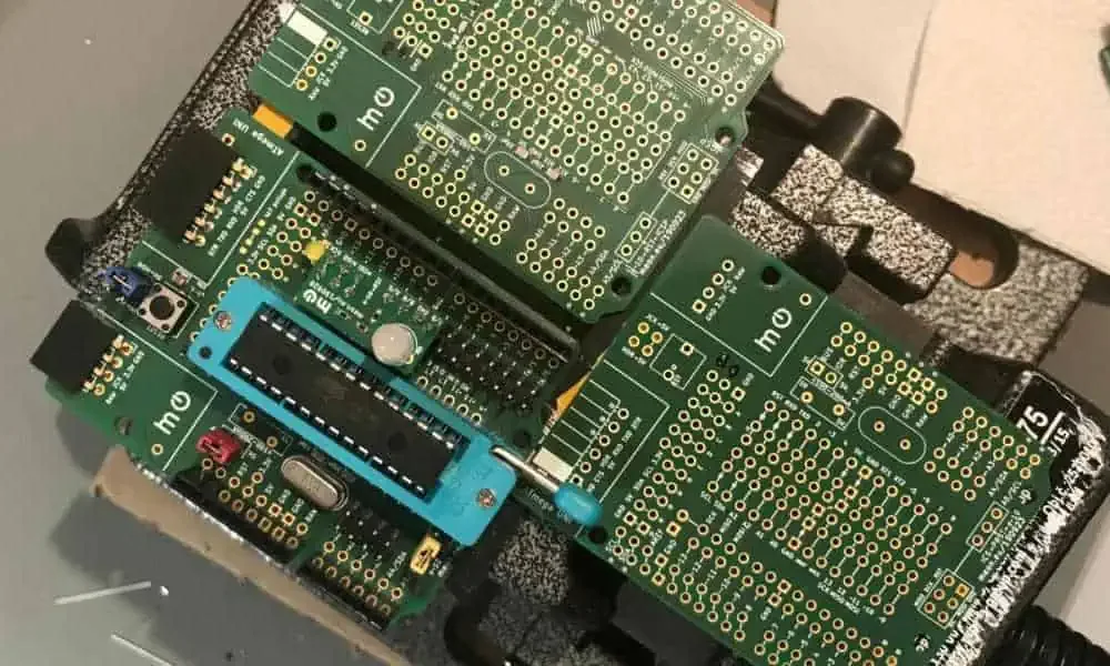
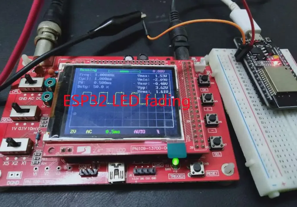
Use the official board resources and schematic to follow functions across the design. The worksheet provides a separate load-power inventory for your own stated scenario; it contains no official UNO current model. Archive photographs show general controller and development-board context, not independent validation of an official UNO R3 unit.
Identify the revision before interpreting labels
Record the exact board and revision under review. The UNO name covers hardware that should not be treated as one universal pinout or electrical implementation. Obtain the corresponding official resource and check that the schematic and board information match the actual target.
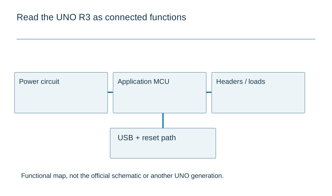
For the UNO R3 reference, distinguish the ATmega328P application processor from the board's other functions. Power management, the USB interface, clocking, reset and connectors support the processor but are not all internal to it. A block-level reading should show those responsibilities separately.
Do not assume an inexpensive compatible board reproduces every reference component. Identify any different USB bridge, regulator or oscillator from its own documentation and schematic. The observable header layout alone does not establish identical startup, driver or electrical behavior.
Follow power from the entry to the load
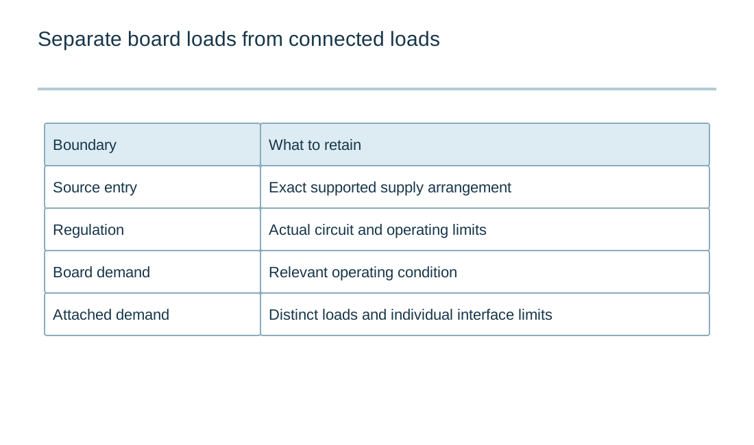
Trace each supported power entry and the circuit that connects it to the board rails. Keep source selection, protection and regulation visible. Reading only a nominal input label can miss the conditions governing an actual power path or the effect of another connected source.
Identify what the board itself consumes and what is supplied to attached circuitry. For a custom load inventory, enter distinct downstream loads in one operating state. The worksheet's illustrative total of 0.829 W comes from fictitious rows and is not a rated UNO output allowance or measured board consumption.
Compare the real application with the exact board documentation and regulator conditions. Supply and pin limits are not interchangeable. An external load that fits a total power estimate can still violate a connector, regulator or I/O requirement. Use the linear-regulator loss guide only for the specific regulator boundary it models.
| Review item | What to establish |
|---|---|
| Identity | UNO R3 reference kept separate from R4 and third-party variants. |
| Power | Actual entry, selection and regulator path to distinct loads. |
| Signals | Header labels mapped to processor functions and resource sharing. |
| Startup | Clock, reset, USB interface and programming responsibilities. |
| Derivative release | Changes, exact files, approved parts and bounded test scope. |
Load power inventory
Load power inventory
Use the current inputs and keep the assumptions
Load the example to learn the worksheet, then clear it before entering your project values. Blank fields are not silently converted to zero. Units and selected conventions belong to the result, so review them together with the numbers. Editing any input invalidates the previous result and disables its download until you calculate again. Edited example data remain labeled as an illustrative example.
This tool runs locally on the values you enter. It does not open a schematic, select approved components, measure signals or inspect a physical board. Keep the exact component documents and a record of measurements with the design. Downloading the text report does not send an enquiry or populate the Contact form. Attach it manually if it helps explain a specific engineering question; completing the worksheet is optional.
| Input | What to establish before using it |
|---|---|
| Review reference | Use a nonconfidential revision reference. |
| Downstream loads · CSV | Use distinct loads in one operating condition. Exclude upstream regulator inputs to avoid double counting. |
Map headers to the actual processor and peripherals
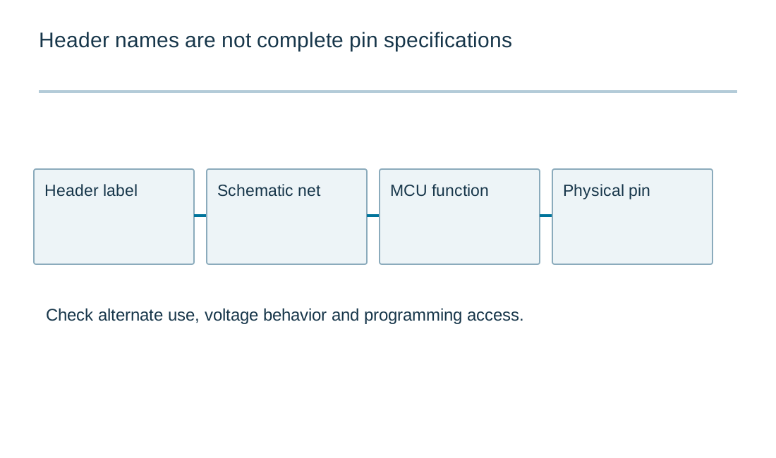
Connect each header label to its schematic net and physical MCU function. Keep analog inputs, digital I/O, power and reference connections distinguishable. A convenient software name is not the full electrical specification of the pin behind it.
Check alternate uses that can interact with an application: serial communication, timers, interrupts and programming connections. A shield or library may depend on one of those resources. Reserve them deliberately instead of assuming that every exposed pin remains freely available in every software configuration.
When moving from the reference to a custom product, use the custom Arduino migration guide. It connects software assumptions and prototype evidence to a new physical design. The present page remains a circuit-reading guide for the UNO R3 rather than a second generic migration tutorial.
Separate USB communication from application execution
Trace the USB connection through its interface circuitry to the application processor. Identify the device responsible for presenting the host connection and the signals used by the programming workflow. A serial port appearing on a computer proves only part of that path.
Keep programming, reset and normal serial communication distinct in the review. A host action can affect control signals as well as data, depending on the actual circuit. Use the USB-to-UART guide to examine logic levels and framed data transfer for bridge-based implementations.
If a reference-derived board uses a different USB interface, preserve the complete change in the schematic and test plan. Driver behavior, configuration and control-line handling may differ even when the application eventually receives the same bytes. A substituted bridge needs its own evidence.
Read clock, reset and programming as one startup story
Identify the clock source and its supporting components for the exact processor circuit. Keep oscillator requirements tied to the selected device and part. A footprint with the right number of pads is not evidence that another resonator or crystal is a suitable substitute.
Follow the reset network and intended programming access. Document the conditions required before firmware takes ownership of pins. If a custom design removes headers or changes the reset arrangement, retain a practical recovery path and an observation method for first-power diagnosis.
The ATmega328P layout guide addresses package-specific hardware implementation. Use it alongside the exact manufacturer documentation if reproducing that processor circuit. Do not transplant the reference's assumptions to another MCU merely because the software environment supports it.
Understand what a reference design does not prove
A published schematic explains a specific design and is a useful engineering resource. Reusing part of it does not independently qualify a derivative board's thermal behavior, EMC, electrical interfaces or assembly process. Changes in layout, enclosure, source and loads can create new requirements.
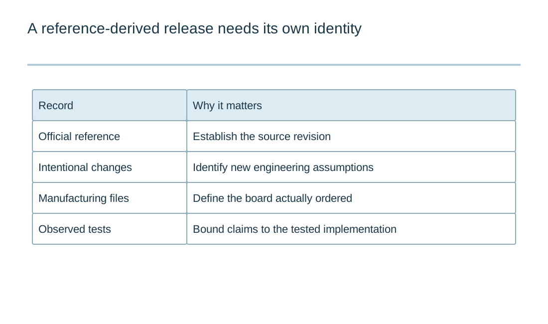
Record the source revision and the changes made. Review applicable licensing and trademark conditions when distributing a derivative design or product. Describe compatibility accurately, without implying official manufacturing or certification on the basis of a familiar board shape.
Keep demonstration code and product software separate in test evidence. A simple example can establish a connection or a peripheral response, but it may not exercise simultaneous loads, failure recovery or the application's timing. Define the actual product acceptance scope before ordering repeated assemblies.
Prepare a controlled reference-derived build
Provide the finished fabrication package, BOM, placement information, quantity and assembly scope rather than only an official reference link. The manufacturer needs the actual revision to be built, including intentional deviations, population options and approved component alternatives.
State the programming image, required interface and post-programming checks if those operations are part of the order. Define which items are customer-supplied and which require sourcing. Those decisions affect a quotation more directly than the broad description Arduino-compatible PCB.
For RAYPCB review, identify the specific construction or assembly question that remains open. A reference schematic and a load calculation can explain context, but they do not replace the controlled build files or establish that a custom design has been validated.
Retain the boundary between a reference and your implementation
Record the exact reference hardware and document revision used for each part of the design. Identify what is retained, what is removed and what is changed. A compatible software environment or matching connector arrangement does not establish that electrical, mechanical and startup behavior are unchanged.
Give each intentional difference an appropriate review or test. Keep the evidence attached to the actual board, fitted parts, firmware and operating setup. This is particularly useful when a development prototype becomes a custom carrier or product board: the earlier demonstration remains valid for its original setup, while the new implementation needs its own observations. A manufacturing enquiry should include the released derivative files and its agreed scope, not ask the receiving team to reconstruct the intended changes from a reference link and informal notes.
Standards, source context and limits
The referenced manufacturer documentation supports specific devices, interfaces or design methods. Apply the version and operating conditions appropriate to the actual part. A similar product name is not evidence that pin functions, voltage tolerance, startup behavior or package dimensions match. Worked examples illustrate reasoning and arithmetic; they are not released schematics or independent hardware test results.
For fabrication scope and the agreed construction requirements, see PCB manufacturing.