Alexa IoT: A Force to be Reckoned With

Alexa IoT

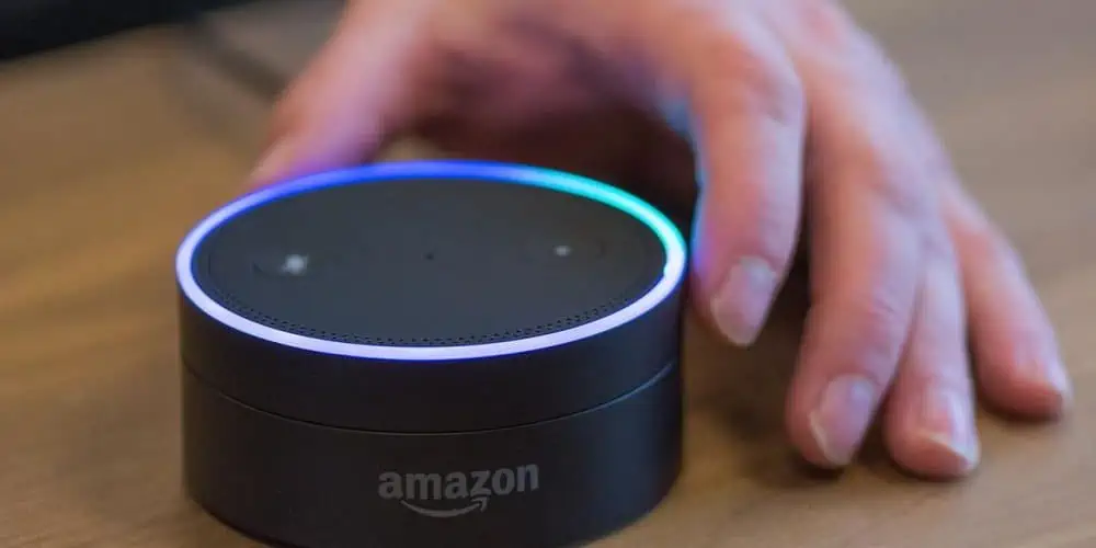
Amazon’s Alexa is the technology that allows you to talk to a computer system by using your voice. This system is connected to the internet and can answer questions, give you weather & sports updates, read news, play sounds from various sources, and do many other things. The device that links to Alexa services is called Amazon Echo.

In addition to its built-in features, Alexa can also work with other devices & services. To access these features, you use voice commands, which are similar to the basic commands. 

Companies and manufacturers are adding Alexa to their devices to improve their operations and increase their business. 

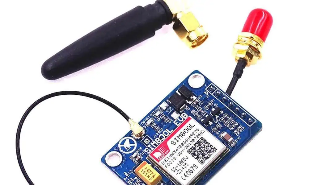
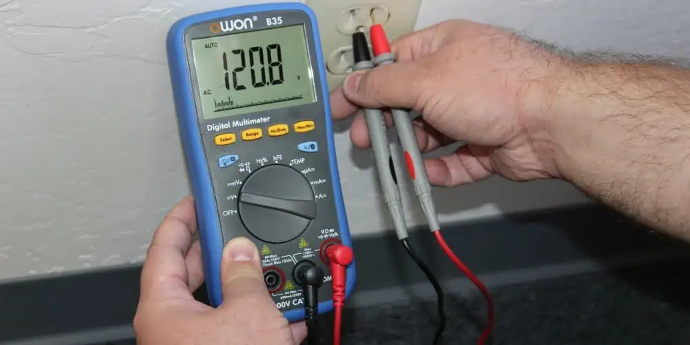
Alexa Iot – Voice Interface To Control & Manage End Devices

Alexa IoT BOARD
Alexa IoT BOARD

The Alexa Skills Kit (ASK) SDKs can create new say commands that work with web services or AWS lambda functions to perform tasks. It helps businesses to add a voice interface to their SaaS frameworks or improve their existing business processes by using voice commands. 

You can connect to the Amazon Alexa IoT ecosystem by: 

  • Utilize Amazon Echo to send voice to Alexa.
  • To make Amazon Alexa work with other devices, you must create a set of voice commands called skill sets. Users can use these commands to control cloud-connected devices through their voice using Echo/mobile app. Every skill set is connected with a specific Alexa API that executes the command. 
  • When you talk to Alexa, your voice command is sent to a special AWS lambda program. The program then figures out what you want to do and sends a message to the device’s cloud to do the action. This program and message system is called Alexa API. 
  • The cloud of the device understands the sms and sends a signal to either turn on or turn off.
  • The Alexa Skills API checks if the message sent to the device’s cloud was successful/not and sent a response message.

Alexa gives the user feedback based on the response received from the device cloud.ย 

YouTube video

Benefits of Alexa IoT

A Gateway can connect IoT devices to perform various tasks in different industries like retail, industrial automation, home automation, automotive, etc

Integrating Amazon Alexa with VOLANSYS’ CENTAURI 200 IoT gateway can provide many benefits to enterprises, such as. 

  • Voice Controlling: By integrating Amazon Alexa with VOLANSYS’ CENTAURI 200 IoT gateway, businesses can benefit from touch-free solutions and advanced capabilities in their operations. Voice control has made IoT( Internet of Things) products smarter & more connected, allowing people to obtain information & control their environment through their tone of voice.
  • A gateway helps people communicate wirelessly between their device and the user.
  • Implementations: Most of the businesses like food and drink, online shopping, and more have been promoting ways to order things on your phone. Now they’re taking it further with say-only ordering, you can do using your Android or iPhone. With Amazon Alexa, you can even order things just by talking! It has made a big impact on how things work in real life. The Echo isn’t just helping businesses, it’s also making a big difference in our everyday lives. 

Alexa IoT for Keeping Devices Secure 

FULL PCB MANUFACTURING Quote

ยท Basic security measures

You don’t need to be a tech expert using IoT ( Internet of Things )devices safely. Here are some simple tips for keeping your IoT devices secure. 

Make sure that the device and router have safe, unique passwords. When you get a new device, it’s important to change the password to something different. If you & your neighbor have the same equipment, you could also have their password, which makes it easier for someone to hack into your device. By changing the password to something unique, you can lower the risk of being hacked. 

ยท Keep the device updated

It’s really important to install updates for your device that become available. Updates often come with security fixes, so they help keep your device safe from hackers. Some devices can update automatically, so you don’t have to worry about it. Also, be careful with equipment that is no longer supported by updates. Technology changes fast, so it’s possible for a device to become outdated and dont get updates sooner than you think!

ยท Use a debit or credit card 

If you’re looking for a safe way to make purchases, a Visa gift card/a reloadable card is a good option. These cards aren’t linked to our bank account, so if someone hacks into the card, they can’t get to your bank account and steal your money.

Donโ€™t link it to your sensitive email accounts. If you connect your equipment to the work email/personal account with sensitive information, hackers could gain access to information that you want to keep private.


Advanced measures of Alexa IoT

If you’re good with technology, you can make your IoT devices more secure by doing these things. 

  • Turn off Universal Plug and Play. This function makes it easy for connected devices to find and talk to each other. But it can also make your device vulnerable to prying hackers.
  • Connect the device to its wifi network. This method ensures that if a device is hacked, it won’t let the hacker access any other internet-linked device.
  • Use restriction: This makes sure that the equipment can only talk to the devices that you have permitted.

Future of Smart Homes with Alexa IoT

Amazon thinks that using your voice to control your home is the future, and it will make using technology much easier. For example, you can ask Alexa to play a song or turn off the lights while you’re in the kitchen washing dishes. Nowadays, a smart house isn’t just about using connected applications and your voice to make things easier at home. You can ask for everyday news or even check the traffic while preparing. 

Connected home and Alexa IoT

Amazon Alexa IoT
Amazon Alexa IoT

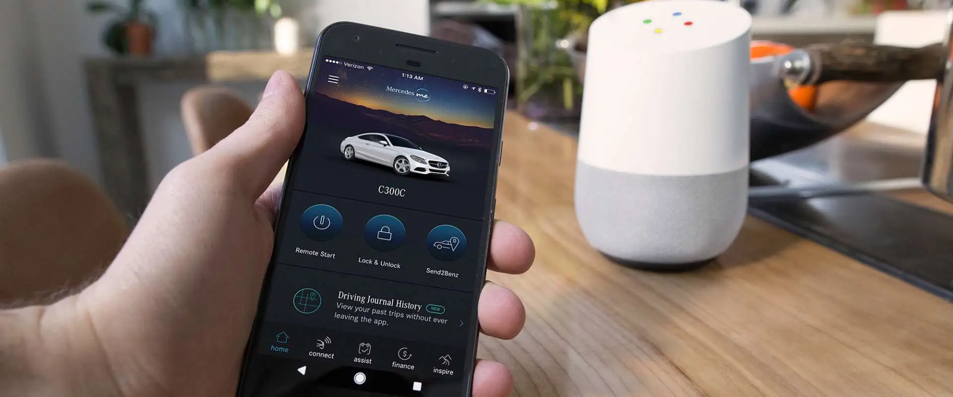
Smart home technology has evolved, & with the recent development of voice-activated assistants like Alexa, people realize that having a smart house is easier than they thought.

In the past, it was a hassle to turn on a smart device because you had to unlock your cell phone, open the app, & press the button. It was easier to get up and do it yourself. Plus, you might have had to use different apps for different devices. But with Alexa and voice commands, you can now control your smart devices just by asking Alexa to do it for you. You can ask Alexa to turn on the lights, lock the door, adjust the temperature, or even order you to ride to work.

Regarding Alexa and making homes smarter, we still feel like we’re just starting. But we’re really happy with how many device makers and software developers are creating cool stuff for Alexa & making it part of their products. 

Biggest Imapcts of Alexa IoT

Alexa doesn’t just make things easier by letting people control their smart homes with their voices. It’s also really helpful for people who are visually impaired/elderly. Lots of those folks have written to us to say thank you for giving them a way to be more independent; now, they can use their voice to control things around them. 

GE is making a new table lamp that has Amazon Alexa built right in. That means you won’t need a separate Echo application to use Alexa – you can talk to the lamp)

Reluctant consumers use Alexa IoT in the smart home

People who are just starting have lots of choices to pick from. 

At Amazon, we want to help people turn their houses into smart homes using Alexa. With Alexa, you can control lights, locks, thermostats, fans, and sprinklers. If you want to set up a smart house independently, choose what you want to control and then check the Amazon Smart Home store to seek the products that work with Alexa. It’s easy!

If you use companies like Vivint/Alarm.com for your home services, they can help set up a smart house system that works with Alexa and fits your needs. As people want smarter homes, we’re teaming up with a group called CEDIA, which helps professionals all around the country install and design smart home systems. 

Alexa IoT Voice Service

AVS is a set of tools that developers can use for free to add Alexa to their applications. All they need is a speaker, microphone, and internet connection, and with just a few simple instructions, they can integrate Alexa into their product. 

GE’s new smart light utilizes AVS to connect Alexa to a modern table lamp. It means that you can light up a room with energy-efficient LED lighting and also access the Alexa features that you would find on an Amazon Echo without needing a separate device. 

A new small lamp is coming out that has a special feature. It has a speaker & microphones that work like Alexa, the virtual assistant in Amazon devices. You can use your voice to ask Alexa to read the news, control your other smart devices, and play music. 

Overall, adding voice control to smart devices has made it very easy to interact with them at home. We think that when people see how easy it is to turn off a light just by speaking to Alexa, they will want to try using other smart house features too. 

How do Alexa IoT Devices Work?

IoT devices are objects that can do different things, but they work in similar ways. They have a computer inside that can sense things in the real world. They use special software and are available together on the internet. To work properly, they need a unique IP address connected to a special server.

To control most IoT devices, you need to use a special app on your phone. This app lets you turn on and off devices like lights in your home. Some devices don’t need an app because they have a built-in server. It means they can work immediately, like when a sensor turns on lights when you walk into a room. 

Examples of Alexa IoT Devices

BlackBerry IoT

ยท Home Security 

The main thing that makes homes smart and safe is IoT. It means that devices such as sensors and cameras are all connected and can be controlled using a smartphone. It makes it possible to have constant security all day and night. 

ยท Activity Trackers 

Cameras that help keep your home safe can send you alerts and make you feel more secure. Activity trackers can sense things about your body and send that information in real time. You use them to check and manage things such as appetite, blood pressure, physical activity & oxygen levels. 

ยท Industrial Security and Safety

You can use IoT technology to detect and monitor restricted areas for trespassers. You can also use special sensors & cameras to check for pressure or leaks of dangerous chemicals. It helps you fix problems before they get worse and cause serious harm. 

ยท Augmented Reality Glasses 

AR glasses are special glasses that have a computer inside them. They show you extra information such as 3D animations & videos on top of what you see in real life. The glasses show you this information through their lenses and can even help you use apps on the internet. 

ยท Motion Detection

Motion sensors feel when dams, bridges, buildings, & other big structures shake or move. They can find problems or things that aren’t normal, leading to bad accidents. You can also use these sensors in places where floods, landslides, or earthquakes might happen.

Unlimited Possibilities with IoT

IoT technology is still very new, and it’s expectable to grow a lot in the future. When we combine IoT with AI, we’ll be able to come up with new and creative ideas that can be used in many different industries.

To have a good career in the Internet of Things (IoT), it’s important to start on the right path &check how the Internet of Things works with technologies. 

The Ultimate Guide to Altium Keep-Out Layer

Altium Designer 20

A user-defined region or perimeter included in the design and which copper items cannot intersect is known as a “Keep out” in the design of PCB. A Keepout is frequently used to restrict the region. It utilizes automatic copper placement procedures like interactive routing and polygon pours. It also designates an improper position when copper items are placed manually.

Keepout objects employ the current Clearance Constraint Regulations to regulate routing and identify positioning violations as designated “no go” zones during design layout; however, unlike other inserted objects, they cannot be allocated to something like a Net, nor are they displayed in produced printouts or Outputs. In the most basic sense, a Keepout functions as such an “interference” item that, in accordance with the worldwide Clearance Rule, prohibits other copper items from overlapping its region.

Through its feature of support for Item Specific Keepouts, Altium Designer makes it possible to create and use Keepouts. It is possible to arrange placed Keepout items to only apply to specific types of objects, including tracks, copper regions, pads, and vias, greatly enhancing the efficiency and flexibility of Keepouts.

Cross-hatching displays Keepout items in the Printed Circuit Board Library Editor and PCB. Keepout objects assigned to a Keep-Out Layer. It displays inside the Keep-Out Layer hue. But Keepouts are set to a particular signal layer. It displays in the hue of this specific Layer.

Keepouts are perfect for designating non-routable circuit board areas like mechanically incompatible parts like mounting holes and the edges of a Circuit, high voltage regions, or electrically sensitive, especially exposed copper spots as in Test Points and Fiducials. After particular Keepout Limitations have been given, the flexible nature of Item Specific Keepouts additionally enables them to also be put across other objects. To limit the scope of automatic Via Stitching, a Keep out sometimes puts over already-existing copper sections like a Polygon Pour when it configures to restrict solely via.

YouTube video

What Is Altium Keep-Out Layer?

First off, Altium is a comprehensive PCB layout software suite that houses several design tools on one platform. The most recent edition of Altium, Designer-20, is a product of several years of invention and development. It aims at creating genuinely integrated design tools. Because of this, the software enables users to make effective use of all aspects of the PCB design process.

Altium is now among the most used Circuit Board design tools, praised for its superb mix of control and use. A user-friendly interface created by Altium’s creators puts all of the system’s capabilities at their fingertips. Broadly speaking, Altium Designer aids PCB engineers in bringing their imagination to life.

The workspace for Altium Designer consists of two essential parts:

  • The very first is Altium Designer’s primary content editing location. It appears on the very right side of the program.
  • The Workplace Panels make up the second location. In addition, some panels spring out from the right side of the tool, most float, while others hide in Altium. Some panels dock on the very left portion of the application.

Placing Altium Keep-Out Layers

Using the Place to Keepout menu, a Keepout is then added to the editor’s design area, where the selected Keepout style, like its Track, Region, Fill, or Arc, is applied to the currently operating Layer. To change the Keepout’s physical attributes, Layer, or item type limitations, choose Properties. These Keep out characteristics are related:

The Keepout Layer is determined by the Banned for Layer, which determines the circuit layer as to which Copper Items are Limited. Choose the Keep-Out Level to create an all-layer keep-out.

Keepout Restrictions specify which object kinds are going to be constrained mostly due to Keepout. By not enforcing the relevant Clearance Rule, deselecting a type of object will result in the Keepout, allowing infractions by that kind of object (which is not specifically kept out).

Availability

FULL PCB MANUFACTURING Quote

The following options are available for placing Track Keepouts in PCB and Circuit Library Editors:

Insert a track or trace keep out within PCB Editor using the following methods:

  • From the main menus, select Location, Then Keep out, Then Track.
  • In the Active Bar menu, which places at the right top of the layout area, select the button in the drop-down menu for graphic objects. (Hold down a button on the Active Bar for additional related commands. Once the command invokes, It will rise to the top of that portion of an Active Bar.)
  • Right-click, From a context menu, select Place, Then Keepout, and Then Track.

Insert a track or trace keep out inside the Circuit Library Editor in any of the following methods:

  • Choose Location, Then Keep out, and ThenTrack from the primary menus.
  • The Active Bar button of the menu is positioned at the very top of the layout area in the drop-down menu for graphic elements. (Hold down a button on the Active Bar to access associated commands. After a command invokes, it rises to the top of that portion of an Active Menu.)

Placement

 As the command executes, the cursor transforms into a crosshair. Then add tracks and keep out placing mode. The steps that follow are used to determine placement:

  • To set the beginning of the initial track, keep out portion; Press or Click Enter. Drag the mouse to create the track keep out section, then click Enter to fix the endgame of this initial part. It also serves as the start node for the subsequently linked segment.
  • Keep moving the mouse to create the associated track and keep-out sections. Then click Enter to attach a set of vertex nodes.
  • To stop the current chain of the linked track, keep out sections, right-click or hit Esc.

In addition, do the following during placement:

  • To stop the placement but also open the Keepout. Track the option of the Options menu using a Tab key. From there, you may quickly modify the placement’s characteristics. To continue placement, press the stop button overlay ().
  • To switch between the usable signal layers, use the * key. Instead, you may use Shift+Ctrl+Wheel Spin to navigate the routing levels. Each click of a mouse scroll wheel will take you to the following or prior signal layer that is now accessible.
  • To cycle among all exposed signal layers, including the Keepout plane, press the + or – buttons on the number pad.

Altium Keep-Out Layer Placement Modes

There are five corner modes that uses while building keep-out track segments. While four of them also include corner directional sub-modes. 

  • During placing: Press Shift+Spacebar to choose between the five corner options that are available.
  • To switch between the corner orientational sub-modes, use the Spacebar.
  • Pressing the. Or, keys while using any of the curve corner modes will cause the arc to either grow or decrease. To hasten arc resizing, press and hold the Shift button.
  • To choose between inserting one part per click and two parts per click, use the shortcut key 1. The look-ahead section refers to the empty track section in the initial mode.
  • To eliminate the final vertex, hit the Backspace button.

Graphical Editing

Using this editing technique, you can choose a track to keep out the item that has been put in the layout area. You can also visually modify its shape, size, or placement.

The subsequent editing interfaces are accessible once track keeps out is chosen:

  • To move the track’s endpoints, touch the endpoint handles.
  • To alter the track’s shape, hit and then drag the middle handle.

Non-Graphical Editing

There are several non-graphical editing techniques accessible.

ยท Editing through the Altium Keep-Out Layer- Properties Panel 

  • This technique of editing employs the affiliated Keepout. Properties panel and Track dialog to change the attributes of the Track Keepout item.
  • Using the Tab key during placement will bring up the Properties panel’s Keepout – Track mode. All choices become available after placing the Track Keepout.

When the Track or Route Keepout object has been installed, it is possible to 

  • Double-click the Track or Route Keepout item after installation.
  • Hovering the mouse pointer above the Track or Route Keepout item and selecting

Properties via Context Menu

The following methods use to access the Keepout – Route or Track mode of the attributes or Properties panel after placement:

  • Choosing the Track or Route Keepout object if, by any chance Properties tab is already open.
  • After choosing the Track or Route Keepout object, choose View, Then Panels, And Then Properties panel from the menu bar. Or click the Panels icon in the Right bottom corner of the layout space to see the Properties panels.

Editing Multiple Objects

Multiple object modification supports by the Properties or Characteristics panel. It allows you to change the settings of properties. A field input in the Properties Menu does not indicate through an asterisk (*) for all chosen objects that can be changed. When various same object kinds select manually, using the Find Identical Objects dialogue, or via List panel or Filter.

Tips From Altium Designer – How To Prevention Design Errors Altium Keep-Out Layer

Some engineers lack a strong background in PCB design. This prevents them from fully understanding certain of the software’s settings and choices. It also prevents them from knowing how PCBs process. There are frequently a number of issues, or the Circuit manufacturer processes the information using the traditional approach. It is unable to grasp the design goal. Let’s look at a few of the mistakes that are simple to commit.

  1. The KEEPOUT layer, or mechanical Layer, shows the board’s form and the non-metalized slot. You must not choose the KEEPOUT checkbox. Choose the checkbox to restrict wiring.
  2. The Multilayer Layer PCB has mechanical slots and holes installed in it. The 3D schematic has holes and slots due to the cutout character, yet the GERBER might not be produced regularly. This leads to leaks. To construct a clear line, it is advisable to place it under the KEEPOUT or mechanical Layer. Avoid selecting the KEEPOUT choice, please.
  3. Neither the high nor the low editions are part-time. The square hole shows in place of the square slots. Using the circular drill, the insert’s slot or hole is there. Thus, the square grooves and also the square holes cannot be formed. A hole in the GERBER data file is round.
  4. Owing to the several editions of the AD program, inversions frequently arise in every iteration. The fact that the premium version isn’t even functional with the cheap version is absurd. Yes, you are correct that the “premium version might not be appropriate with the cheap version.” Thus, we advise customers to generate the GERBER format file. Check it, and afterward, make their purchase. If they choose not to do so, please remember to identify the design software version while doing so.

GSM PCB Antenna: The Ultimate Networking Solution

gsm pcb antenna

GSM allows us to use our phones to talk and transmit data wirelessly. Bell Laboratories created this technology in 1970 using a handheld two-way radio device. In 1982, a group called GSM was formed to develop a European mobile phone standard. GSM technology is trendy and used by over 70% of people with digital cell phones. It was created using digital technology and is now used by over 1 billion people in more than 210 countries. GSM allows people to use their phones to talk and send data and handle all kinds of services. This article is just an introduction to GSM technology.

GSM (Global System for Mobile Communication) is a modem for mobile communication, which means it helps our phones connect to the internet and talk to other people. It was created at Bell Laboratories in 1970 and is now used worldwide. Moreover, Global System for Mobile Communication is a digital technology that lets us use our phones for talking and sending data. It works at different frequencies, such as 1900MHz, 1800MHz, 900MHz, and 850MHz.

GSM technology is a type of digital communication system that uses something called the TDMA technique to work. It turns our voice and data into digital information and sends it through a channel in 2 different streams, each with its particular time slot. It can carry data quickly – from 64 kilobits to 120 megabits per second. 

In a Global System for Mobile Communication system, there are different sizes of areas called “cells,” such as micro, macro, pico, & umbrella cells. Every cell size depends on where it is being used. There are five various cell sizes in a Global System for Mobile Communication networks, and they vary in how big of an area they can cover depending on the environment.

Moreover, the TDMA technique works by giving different users their time slots on the frequency. It can handle voice and communication well and carry data from 64 kilobits to 120 megabits per second. 

YouTube video

What is GSM PCB Antenna?

The CTRF-ANTENNA-PCB-GSM-3208-UFL100 is a PCB Antenna used for GSM and GPRS connections. It’s a small PCB antenna, about 32x8mm, with a connector called Ipex/U.FL/MHF. 

What is MSC?

The MSC is like the brain of the Global System for Mobile Communication network system. It’s in charge of all the portable units within its service area, and it makes sure that calls get appropriately connected. 

An MSC is also like a bridge between the GSM system & some communication networks that are available to the public. It helps users to access different services, and it’s essential for making connections between various networks possible. 

What is the function of the GSM PCB Antenna or MSC?

The MSC uses three databases (VLR, HLR, and AUC) to get all the information about a user’s location and call requests. It updates some data in these data sets based on things such as location updates or changes in network coverage. 

The MSC is like the heart of a network, and it has many important jobs to do. It makes sure that mobile devices are registered in the right location and that they can move between different zones and networks without any problems. It also keeps track of phone numbers and ensures that calls are sent to the right place. Additionally, the MSC has other vital functions, such as controlling the volume of calls and making sure the network doesn’t get too busy. 

The MSC also helps manage the channels that are useful for communication, and it makes sure that data is transmittable securely and kept confidential. It includes checking that devices are best to use the network, encrypting information to keep it safe, and identifying mobile devices. 

What is a GSM PCB Antenna High-performance Flexible Antenna?

The CTRF-ANTENNA-FPC-7027-7015-IPEX-120 is a high-performance antenna that can be used with 4G GSM networks. It’s flexible, and it has a frequency range of 698 to 960MHz, 1710 to 2170MHz, and 2300 to 2700MHz. C&T RF Antennas Inc makes it. 

The 4G GSM Antenna is a small and flexible PCB antenna that measures 70x15mm. It comes with an Ipex connector and a 120mm cable, and it’s best for use in 4G, 3G, 2G, GSM, GPRS, and NB-IoT devices.

What is 4G GSM PCB Antenna frequency?

FULL PCB MANUFACTURING Quote

GSM operates at two frequency bands: 900 MHz & 1800 MHz. The TD-SCDMA technology works at 1880 to 1920 MHz and 2010-2025 MHz frequency bands, while The 4G frequency bands that use both TD-LTE & FDD-LTE technologies are 2320-2370 MHz, 1880-1900 MHz, & 2575-2635 MHz.

Global System for Mobile 

The communication network plays a crucial role in mobile communication. Moreover, Several companies such as M1, Telstra, AT&T, Singtel, and StarHub have said they will turn off their GSM networks.

In China, the TDD-LTE mobile network has been available for a year, and the older GSM network has become outdated. With the fast growth of the internet, the GSM network cannot handle the demand for data services. Also, the GSM system uses valuable low-frequency wireless resources that are not useful well.

Despite the availability of new mobile network technologies, the GSM network still has advantages in terms of voice service and coverage. Operators still earn a significant portion of their revenue from language communication prices, and the Global System for Mobile Communication network is essential for providing voice assistance on 4G networks. However, maintaining and optimizing the Global System for Mobile Communication networks requires investment. 

C&T RF Antennas Inc is a producer in China that supplies flexible PCB antennas for 2G, 3 G, 4G, 5G, and 6G built-in antennas.

Features of the GSM PCB Antenna

There are many characteristics of the Global System for Mobile Communication module, such as:

  • Improving Spectrum efficiency 
  • Supporting International roaming
  • The system is suitable for coordinated services. 

Digital network (ISDN)

  • Supports new services
  • Allows for SIM contact management
  • Allows FDN function
  • Has an RTC alarm management
  • Provides quality speech during calls
  • Utilizes encryption to enhance the security of phone calls
  • Supports SMS

The Global System for Mobile Communication is currently the best secure telecom protocol. Even though the privacy of the call and the subscriber’s identity is only on a radio channel, it is still an essential step in achieving overall security.

GSM GSM PCB Antenna

A Global System for Mobile Communication modem is an application that can be used to connect a computer or other processor to a network. It can be a modem/mobile phone. Moreover, It needs a SIM card and access to a network subscribed to by a network operator. This device is connectable to a computer using a serial port, USB port, or Bluetooth. 

A Global System for Mobile Communication modem can act as a mobile phone or a modem to help a computer communicate over a network. It needs a SIM card to work and uses the network range subscribed by the operator. You can connect it to a computer through a serial, USB, or Bluetooth connection. It can also be a regular GSM mobile phone with a suitable cable and software driver. The GSM modem is preferred over a mobile phone and is used in various applications such as supply chain management, transaction terminals, security, remote data logging, and weather stations.

Applications of GSM PCB Antenna

GSM technology can be useful in the following ways 

GSM Technology for Automation & Security

Nowadays, we always carry our GSM mobile phones with us, like our purse, keys, or watch. This mobile phone allows us to communicate with anyone in the world. Being able to contact someone or being approachable by anyone important to people. 

This project uses Global System for Mobile Communication network technology to send and receive SMS messages between a sender and receiver. The SMS feature is useful to remotely access and control home appliances, as well as provide security monitoring. There are two sub-systems: the appliance control system and the security alert system. 

Moreover, The system can send SMS messages from a particular cell no. to control home appliances and ensure their security. The user can change the appliance settings remotely according to their needs. Additionally, if there is any trespassing, the system can send automatic SMS alerts to the user, warning them of the security risk. 

GSM technology lets people communicate with others anytime and anywhere. The system uses intelligent networking principles, ensuring compatibility with different devices. This approach is the first step towards developing a communication system that can be accepted widely.

GSM PCB Antenna Applications in Medical Services

“Imagine two situations described below.”

Imagine two situations such as:

  • Someone is very sick and needs help urgently, but they only have a smartphone to ask for assistance.
  • A patient got leave from a hospital and wants to rest at home but needs regular check-ups. They may have a cell phone & medical sensor tools such as health monitoring tools.” 

In these situations, the solution is to use a wireless communication system. Using communication technologies, patient details are transferable through the network.

In the first case, the doctor monitors the patient’s information and provides instructions so that they can take precautions before going to the hospital. In the second case, the doctor monitors the patient’s test results and takes the necessary steps for more treatment if abnormalities occur.

This entire process is telemedicine services. There are three ways to use a telemedicine system.”

  •         Video conferencing allows patients to interact directly with healthcare providers from one location, and treatment can be carried out accordingly.”
  •         Health-checking sensors keep track of the patient’s health and guide healthcare providers in treatment.
  • Transmit the medical data for consultation & processing. 

“Wireless communication is useful in three ways. Medical services need different ways to access stored resources, such as medical databases/online devices to check patient health. There are three options for accessing these resources: broadband network, intermediate capacity media, and GSM for narrowband access.

“The benefits of using Global System for Mobile Communication technology are

  • It is cheaper.
  • You can find GSM receivers in many devices, such as mobile phones & GSM modems.
  • It can transfer data quickly.

How to Find Fault in PCB Board

how to find fault in pcb board

Are you constantly puzzled by your PCBs’ failures, stuck in a frustrating cycle of plating voids, acid traps, and solder bridges? Are you tired of putting your heart and soul into building a masterpiece only to watch it spectacularly crash and burn? Well, worry no more! While repairing PCB failures can be intimidating, it’s easier than you may think with the right tools and knowledge. Repairing a faulty PCB involves standard soldering, component replacement, and reflowing methods. Understanding the risks involved is crucial as taking precautions to avoid damaging the PCB or injuring yourself. So let’s dive into the fascinating world of PCB faults and discover how to troubleshoot them effectively!

YouTube video

PCB Faults

PCB faults refer to issues with a printed circuit board (PCB), such as incorrect component placement, faulty soldering, incorrect circuit design, or physical damage. These errors can result in malfunctions or failures of electronic devices, requiring costly repairs or replacements. Therefore, debugging PCB faults is essential in ensuring electronic products’ quality, reliability, and efficiency and involves identifying and correcting any errors or defects in the PCB design or manufacturing process.

Why do PCBs Fail?

find fault in pcb board

1. Solder Bridges

When you solder two pads on a printed circuit board (PCB), an undesirable electrical connection results. This connection is a solder bridge. Excessive solder on nearby pads or the absence of a solder mask layer between the pads can result in this. The electrical connection that results may result in short circuits and other issues. To prevent solder bridges, PCB designers must ensure that solder mask layers are applied correctly, and that solder mask layers are present between adjacent pads.

2. Acid Traps:

Areas on a PCB called “acidic traps” are prone to catching and keeping corrosive leftovers like acid flux. Acid traps are frequent in recessed regions or tight spaces, such as between components. These corrosive residues can harm the PCB and cause corrosion, resulting in electrical shorts and other issues. Therefore, large open spaces between components and solder mask layers should be helpful when designing PCBs to protect recessed areas from acid traps.

3. Plating Voids:

When a hole in a PCB partially has plating material, we can refer to it as a plating void. This can occur when you improperly carry out the plating procedure or when the hole size needs to be more significant for the plating material to fill. In addition, plating voids can bring on electrical shorts, limited current flow, and other issues. Therefore, PCB designers should ensure that they carry out the plating procedure appropriately and that the size of the holes is compatible with the plating substance to prevent plating voids.

4. Environmental Factors:

Environmental factors like humidity and temperature can significantly affect how reliable PCBs are. Components can expand and compress under the influence of high temperatures, resulting in fractures and other mechanical issues. Electrical shorts and component corrosion are both effects of high humidity. PCB designers should build their boards to resist severe temperatures and humidity levels and employ protective coatings to stop corrosion to avoid these issues.

5. PCB age:

PCBs’ performance might deteriorate over time for several reasons. First, components may become more fragile and shatter more easily. Second, electrical shorts can result from connections that become loose. Third, corrosion in plating might lead to electrical issues. To avoid these issues, PCB designers should make their boards as durable as possible and utilize corrosion-resistant coatings.

Types of faults in PCB 

FULL PCB MANUFACTURING Quote

1. Soldering fault

Soldering problems account for the majority of the printed circuit board flaws. Using the tiny components present on a PCB board makes the technical skill of soldering even more challenging. However, we can reduce soldering faults during design phase and the soldering procedure. The following are some typical soldering flaws:

When your solder fails to connect with a given point of contact properly, often the pad, the open joints, also known as “dry joints,” result. As solder may be present making poor or sporadic contact, the open joints may not always result in a circuit failure. The open joints can result from physical bending or movement, the wrong solder temperature, faulty designing or manufacturing processes, impact during usage or transit, and shifting.

2. The temperature fault:

The printed circuit boards’ operation may degrade due to temperature when stored and attached to components. Parts or joints may break or fail due to extreme temperatures or significant temperature variations. Many assume the highest or lowest safe temperature without considering temperature variations during use or storage. Temperature changes can result in expansion and contraction too quickly, leading to the PCB failing before it should.

3. Plating fault

Electricity travels through holes from one given side to the other of the board. During manufacturing, the engineer plates the hole wall. During this, the operator deposits copper in the endplate part to establish electrical conductivity with reference to the top. An incorrect copper deposition will result in plating voids, which leaves the wall areas without copper coating. We can blame this to tainted materials, air bubbles, contamination occurring in the holes, and other related causes. You can stop this by adhering to the manufacturer’s instructions and clean the equipment appropriately as directed.

4. Electromagnetic Compatibility fault

We link electromagnetic compatibility (EMC) and Electromagnetic interference (EMI) to PCB manufacturing process. While the latter phrase refers to the harmful effects of EMC, the former is typically employed in production and transportation of electromagnetic radiation. These problems may result from design faults, but we can quickly resolve them by reducing the ground surface of the board.

5. Non-wetting fault

The PCB finish dramatically affects the reflow of the solder and the amount of wetting that occurs. With a poor finish and a lot of exposed bare board, the solder reflows with more challenges and poorly adheres to the PCB. In addition, a prolonged storage period makes soldering more challenging and increases the risk of non-wetting. In most cases, solderability and plating thickness have a direct correlation. The plating required for optimum solderability may deteriorate over an extended storage period. Therefore, a PCB in storage for about a year or longer may be more susceptible to non-wetting and poor solderability.

Methods of finding fault in PCB board

PCB fault
PCB fault

Visual inspection:

This is the quickest type of examination and most widely applicable method for spotting PCB problems. Therefore, we must visually inspect for any obvious evidence of damage, such as cracks, scratches, or burn marks.

Physical inspections:

You can use a multimeter test the resistance and continuity of various PCB components. It can be helpful to identify any open or short circuits.

X-ray examination: 

X-ray inspection is a method for spotting faults that are difficult to see with the unaided eye, like microscopic cracks or hidden solder joints. Using X-rays, the designer can scan the PCB to create an image that is easy to check for defects.

In-Circuit Testing (ICT):

ICT, also known as in-circuit testing, involves inspecting the PCB while it is in use to check for any defects. First, by modeling the PCB’s operation and with specialized testing tools, it looks for any irregularities. Next, put the PCB through its paces during Functional testing: functional testing to ensure that it performs as intended. It is often conducted after completing all other testing and can help identify any performance issues with the board.

Thermal imaging:

This process involves using an infrared camera to identify any hot spots on the PCB. In addition, it might help find any damaged components that are generating an excessive quantity of heat.

The procedure for repairing a faulty PCB

When a PCB fault occurs, repairing it can be a challenging process. However, with the right tools, techniques, and knowledge, it is possible to fix many types of PCB faults. Here is a step-by-step procedure for repairing a faulty PCB:

Step 1: Take out the damaged component or pad

Please remove the damaged or defective components or pads to fix a broken PCB. This step may entail carefully removing the element from the board without harming the nearby circuitry using a soldering iron or desoldering tool. In addition, it might be necessary to carefully scrape away the damaged pad with a sharp instrument or blade if it has any damage.

Step 2: Remove the solder and clean the track.

The next step is to clean the track and remove any extra solder or debris after removing the damaged component or pad. Using a soldering iron or desoldering pump, you can carefully heat and remove the solder. Alternatively, gently clean the region around the track using a fine wire brush or abrasive pad.

Step 3: Cover the track with your copper tape.

Next, cover the damaged track or pad with copper tape once you have cleaned the region. You can remedy this by carefully putting a piece of copper tape over the damaged section after cutting it to size and ensuring it extends the track’s whole length.

Step 4: Solder the joints.

The next step involves soldering the joints to firmly attach the copper tape to the board. To achieve this, carefully apply solder to the joint while heating the soldering iron, not overheating the board or harming any nearby components or tracks.

Step 5: Repair the PCB through-hole.

It would be necessary to return the hole in the PCB to its original size and form if you had placed the damaged component through it. To accomplish this, gently remove any extra solder or debris from the hole using a tiny drill bit or reamer, not harming any nearby tracks or components.

Step 6: Insert and solder your component.

Now, please replace the new component and solder it onto the board after you have repaired the hole. To accomplish this, carefully align the element with the repaired hole and solder the leads or pins to the proper board pads.

Step 7: Remove any extra tape from the mended area.

Removing any extra copper tape from the repaired area after soldering the component into place is crucial. To do this, please use a sharp blade or pair of scissors, careful not to harm any nearby parts or railroad tracks.

Benefits of debugging PCB Faults

SMT Engineers
SMT Engineers
  1. Cost saving

Cost reductions are one of the critical advantages of debugging PCB mistakes. You may save on pricey rework and recalls by spotting and fixing problems early in the design or production process. The cost of replacing or repairing a malfunctioning unit might be high when you put a product with a faulty circuit board on the market. By debugging PCB defects, you can find these problems before manufacturing and resolve them before they become expensive.

  • Improve product quality.

Troubleshooting PCB issues might enhance the final product’s overall quality. You can lessen the chance that a product will fail by locating and fixing problems with the PCB design or manufacturing procedure. This strategy can boost client satisfaction and lead to repeat business.

  • Improved effectiveness

Debugging enables targeted improvements and efficiencies by identifying particular PCB design or manufacturing issues. As a result, you may decrease the time and resources needed to make PCBs by optimizing the design and manufacturing processes, boosting productivity and profitability.

  • Increased reliability

Identifying and fixing circuit board flaws can enhance the final product’s dependability. A faulty circuit board may cause a product to fail, which could be expensive and harm a company’s reputation. Ensuring the circuit board is error-free increases product dependability, lowers the likelihood of failure, and lengthens product life.

  • A better understanding of the design

We can better understand the PCB design and manufacturing process through debugging, which helps with design and process optimization. Engineers can pinpoint areas where the design or manufacturing process might be improved by examining issues that arise throughout the debugging phase. This action enables more effective manufacturing techniques and better designs.

Conclusion

It is evident from the above article that PCBs can malfunction in various ways. Several things might cause a defective board, including solder bridges, acid traps, plating gaps, environmental variables, and PCB age. Fortunately, finding and fixing these flaws is possible if you have the necessary equipment and skills. Once you’ve completed all these laborious steps and repaired your damaged PCB, the item should be in working order. With the right equipment, expertise, and understanding, repairing a defective PCB is achievable, even though it may appear difficult. It may take some time and effort, but the sense of accomplishment when the device works again is worth it! With out-of-the-box thinking, anything is possible. Now, let us hope that our PCBs are up to the task!

How to Design PCB Antenna

PCB Antenna Design

There are different types of antennas. PCB antenna can be printed, thereby, enabling designers to have access to unique architectures and totally custom designs in an assembly. Furthermore, PCB antennas that operate at high frequency allow communication between devices at long distances. These antennas offer several benefits. For instance, they minimize the physical footprint and as well reduce the cost of maintaining a device.

A PCB antenna should be small in size as this helps to improve efficiency. This requires attaching many microstrip patches together. The wavelength of the operating frequency determines the size of the patches.

What is a PCB Antenna?

An antenna used in a PCB is a transducer that transforms current waves in an electromagnetic waves. This antenna is designed to convert current into EM waves in high frequency. A high frequency PCB comprises two antennas. These antennas are attached in the circuit board as an etched copper structure. One of the antennas functions as the transmitted radio frequency signal while the second one functions as the reflected RF signal receiver.

The high-frequency circuit usually produces RF waves and then evaluates the RF wave signals reflected. The base materials of the circuit board transfer the signals to the PCB antenna. Since the PCB antenna is usually compact, it improves efficiency. Also, the antenna combines several microstrip patches to achieve a gain from the compactness of the antenna.

A PCB antenna can be semi-directional, directional, and omnidirectional. An omnidirectional antenna transfer signals in all directions. A semi-directional antenna is for a fixed angle in which the signal propagates. A directional antenna features a single direction in which the signal is required.

To have a good understanding of how a PCB antenna works, it is important to know some details about resonance circuits and impedance matching.

YouTube video

Types of PCB Antennas

FULL PCB MANUFACTURING Quote

Antennas make up a high frequency PCB and PCB antennas are attached to it. These parts of a circuit board are available in various types. So, what are the types of PCB antennas?

Patch antenna

The look of thus antenna is similar to that of a circular or rectangular patch of copper in a circuit. Patch antennas operate at microwave frequencies since short wavelengths can design small-size patches. Portable devices mostly integrate patch antennas since these antennas offer ease of design.

Loop antenna

Loop antenna is the simplest PCB antenna. This antennaโ€™s look s similar to a rectangular or round lop. The copper material used in this antenna and the size of the loop determine its efficiency. As regards wavelength, a loop antenna is not ideal for transmission. However, it is widely used as receptors. Since the loop antenna operates in a directional pattern, it helps to locate the transmitter known as radio direction finding (RDF).

PCB Antenna Layout
PCB Antenna Layout

Slot antenna

It is called slot antenna due to its structure. This antenna comprises a metal plate which has many cuts or slots in it. The electric and magnetic fields in this type of antenna are usually opposite. Slot antenna is widely used in applications such as phased arrays and aircraft radars.

Inverted-F

The inverted-F antenna is widely integrated in the WLAN hardware of our cell phones. As an omnidirectional antenna, the Inverted-F has a large ground plane that helps to ensure maximum efficiency. Copper isnโ€™t used in some part of F patch.

Meander line antenna

A meander line antennaโ€™s conductors are usually folded back and forth. This makes the antenna shorter. Therefore, this helps in achieving a compact size antenna with great efficiency and loss of radiation resistance. Also, this antenna offers decrease in bandwidth.

Guidelines on How to Design PCB Antenna

850 900mhz band PCB Antenna

Since antennas are sensitive to their environment, it is important to consider the layout and design as regards the requirements. Otherwise, this may have a negative effect on the functionality of the wireless device. Minute details such as layer thickness, material, and layer count can impact the performance of an antenna.

Therefore, there are some guidelines that will help you design a PCB antenna successfully. These include:

Antenna positioning

PCB antennas have various operation modes. However, there are some particular positions you need to place them based on the antennaโ€™s radiation level. For instance, you can place them in the corner of the circuit board or along the short side of the board. There are different designs for antennas that are ideal for various positions. Therefore, PCB designers can choose the antenna based on their layout and application.

Closeness to other components

During the design phase of a PCB antenna, you must ensure the embedded antenna isnโ€™t close to other components on the circuits. The height and width of the component determines the distance between other components and the antenna. Components such as LCD s and batteries can have switching speeds. This can help with more signal interference during the functionality of the device.

Keep-out area

Designer need to be sure the components arenโ€™t positioned in the near field around the antenna. Otherwise, this may cause signal interference, which impacts the functioning of the circuit. Furthermore, ensure the area around the antenna isnโ€™t in contact with metallic objects.

Ground planes

The ground planeโ€™s size on a circuit board is a crucial factor you need to consider. This is because wires used for creating communication between different batteries and devices may change if not properly designed. Therefore, designers need to ensure proper sizing of the ground planes. If properly done, batteries and cables linked to the device have less impact on the antenna.

Design the transmission line

In PCB antennas, the transmission line is an RF trace which transmits RF energy. Designers need to design the transmission line at 50ฮฉ as this may reflect signal to the reception. This may result in a degraded signal-to-noise ratio.

Fundamentals of PCB Antenna Design

PCB Antenna Layout
PCB Antenna Layout

Antennas serve two basic functions. These include the emission of electromagnetic waves when there is a current and a voltage. Also, they get electromagnetic waves and transform them into a current and a voltage. The interconnect will have to transfer a signal into the antenna or receive a signal from it.

Furthermore, PCB antennas are usually designed to pick up a magnetic or electric field. Magnetic antennas integrate a loop of wire. The receiver/transmitter element in this system functions in a similar way with a load that completes a circuit board that features the loop antenna.

The physical design of an antenna

A designer aims to define an antennaโ€™s geometry so that they can meet some operating goals such as feedline matching, high radiation efficiency, sufficient bandwidth, directionality, and low loss along front end and feedline. The positioning of an antenna and its physical design will determine these operating properties.

PCB antennas make use of wave resonances present within the structure of the antenna to form a string current oscillation. With this, designers would be able to achieve magnetic and electric field generation around the antenna. Therefore, one of the drawbacks of antenna design is determining the resonances in the structure of the antenna.

After the designer determines the electromagnetic field around the antenna, he determines the radiation efficiency and radiation pattern with software.

The input impedance is another physical aspect to consider for an antenna. You need to know that PCB antennas can posses a reactive component on the input impedance. This will determine how a matching network should be designed for the antenna.

Feedline Design

It is important to design antenna feedlines to get a signal from conductive feedline. This has to be a part of a transmission line designed for a particular impedance that tries to match the impedance of an antenna. Transmission lines are resistive in their characteristic impedance. However, PCB antennas can feature a reactive component.

Therefore, feedline should be designed in a way reduction occurs in the return loss along the feedline. If the feedline isnโ€™t properly implemented, it can limit the bandwidth. Therefore, it is crucial designers choose the right matching method for their exact antenna.

How to Achieve a Better Performance When Designing a PCB Antenna

5G Microstrip Antenna

There are different ways you can improve the performance of your PCB antenna. Below are some ways:

  • Integrate matching networks when during antenna tuning. This helps in compensating for factors that may impact the performance of the antenna.
  • Avoid designing an external casing for an antenna as this may interfere with the signal.
  • Ensure the ground plane you selected is appropriate. If not, this will result in crosstalk between the signals.
  • Do not place the PCB antenna too close to plastic surfaces.  Doing this can have a negative impact on the performance of the antenna. Furthermore, plastic usually features a higher Dk than air. This impacts transmitted signals and can cause losses.
  • Consider the signal bandwidth when designing a PCB antenna.

Conclusion

Antennas serve two basic functions. These include the emission of electromagnetic waves when there is a current and a voltage. Also, they get electromagnetic waves and transform them into a current and a voltage. Learning how to design PCB antenna requires following certain guidelines to achieve the best result.

Explaining the Electrical Impedance Formula

impedance control pcb

Electrical impedance plays a crucial role in the way electrical devices function. It is an important and popular concept in physics and electrical engineering. Impedance is the resistance put up by a circuit to an alternating current like an audio signal. In a resistive circuit, impedance and resistance are similar. The electrical impedance formula helps in determining a circuitโ€™s opposition to a current when voltage exists.

Impedance is mostly used when a loudspeaker connects to an audio system. Although the concept of impedance is not fully understood, this concept is widely used in several engineering disciplines. As an important concept in electrical engineering, engineers use the electrical impedance formula to determine a lot of factors in electrical devices. This article describes a combined impact of electrical impedance in an entire circuit.

YouTube video

What is Electrical Impedance?

Electrical impedance measures the opposition of a circuit to a current when there is voltage. It simply describes the opposition offered by a circuit to alternating or direct current. The symbol โ€˜Zโ€™ denotes electrical impedance. Electrical impedance is usually measured in ohms. Impedance has both phase and magnitude.

The circuitโ€™s frequency determines the opposition of electrical impedance to current. On the other hand, resistance (R) measures how much a substance opposes the passage of electrons among its atoms. Resistance is different from impedance as it contains only magnitude. It can simply be understood as impedance with a phase angle of zero.

Impedance may feature inductive reactance (XL), resistance (R) and capacitive reactance (Xc). Therefore, total impedance is simply the sum of capacitive reactance, resistance, and inductive reactance. Impedance explores the idea of resistance to an alternating current.

The electrical impedance formula is

Z=VI

Where Z is the electrical impedance measured in ohms

I is the electric current usually measured in amperes

V is the voltage measures in volts.

Electrical impedance affects the propagation of signals via a circuit board, the leakage of signals in undesired parts of a circuit board and how power exchanges between components. The effect of resistance and reactance in an AC circuit is usually termed as impedance. The resistance is the opposition of current while reactance opposes electric current flow as a result of frequency dependent elements such as capacitor inductor.

In an AC circuit, the opposition caused by reactance and resistance in the flow of AC is impedance. Therefore, the impedance of an AC circuit in a mathematical perspective is Z=R+- jX. In this case, X is the reactance and R is the resistance.

How does Impedance Differ from Resistance?

FULL PCB MANUFACTURING Quote

Before we discuss the difference between impedance and resistance, we need to understand that impedance is related to alternating current while resistance is related to direct current.

Impedance and resistance are two different concepts. While the two concepts can be used in a confusing manner, there are completely different. Impedance measures the extent of opposition of the AC created as a result of capacitance and inductance. Frequency determines the extent of this opposition. Impedance is simply the sum of reactance and resistance.

Resistance, on the other hand, results from the collision of the electrons present in a conductor with the iconic lattice of the conductor. This in turn leads to electrical energy conversion into heat. One could denote that electrical resistance is simply the opposition to electric current. A good resistance changes with frequency.

Impedance is mainly used in alternating current (AC) circuits while resistance is mainly used in direct current (DC) circuits. Also, impedance occurs as a result of resistance and reactance while resistance occurs due to resistive elements.

While impedance has a magnitude and a phase angle, resistance has no phase angle and magnitude. Electric impedance shows energy stored and power dissipation when it is in an electromagnetic field while resistance only reveals power dissipation.

How does Electric Impedance Work?

Electrical impedance is relevant when AC signal is the applied input signal. In a way, electrical impedance shares some properties with resistance. Also, this means the opposition to current flow. However, resistance is independent of frequency. For instance, if you have a simple resistor and you operate DC voltage, the resistance value wonโ€™t change in response to frequency.

A circuitโ€™s impedance, on the other hand, changes in response to frequency since it has reactive elements such as the inductor and capacitor. In the case of the capacitor and the inductor, these elements offer a resistance referred to as reactance. The symbol X denotes reactance. Capacitive reactance, also denoted by symbol XC while inductive reactance is represented by the symbol XL.

The inductive reactance will have a value equal to jwL while the capacitance reactance has a value that is equal to 1/jwC. It is important to know that this reactance refers to the ratio between the electric current and the voltage. Therefore, if we consider the ratio of the current and voltage, this will amount to the reactance of the capacitor or inductor.

How to Derive Expressions

From the above explanations, you will realize that the capacitive reactance and inductive reactance are dependent on frequency. This indicates that the value of reactance will change in response to frequency.

Letโ€™s imagine your circuit has the resistive elements, the impedance is the total resistance the circuit provides. The symbol Z represents this impedance. Therefore, the total impedance will be the aggregate sum of the resistive element and also the reactive element. The total impedance will then be equal to R+jWL.

In some cases, it is denoted in the polar form. It indicates that there are some finite phase and finite magnitude. The magnitude of such impedance will be expressed as |Z|=R2 + X2 while the phase of the impedance will be expressed as =tan-1(X/R).

Just like the resistance, the impedance of a circuit is also a ratio of current and voltage. Therefore, if the impedance of any circuit is represented in this way, it indicates the voltage will clearly lead the current and the ratio of the current and voltage signal will provide the value of the impedanceโ€™s magnitude.

Types of Electrical Impedance

Edge-Coupled Stripline (symmetrical) pcb impedance control

Electrical impedance is available in two different types. These are the output impedance and input impedance.

Output impedance

For instance, when the circuit gives output voltage when we connect some load at the output terminal. Also, the output voltage must show up across the loadโ€™s two terminals. However, from this perspective, it will find some resistance in electric series.

Input impedance

This kind of impedance occurs when you connect some voltage source through the input terminals. When we look at the electric circuit from this opinion, the impedance in this electric circuit is what is known as input impedance. Therefore, input impedance is simply an impedance between the two terminals of an electric circuit.

Applications of Electrical Impedance

Impedance is applicable in different scenarios. This concept even exists in your house. A panel which comprises fuses controls the electricity of your house. Therefore, when there is an electrical surge, the fuses will disrupt the power to prevent or minimize injury. These fuses work in a similar way with a high-capacity resistor. Without these fuses, the electrical system in your house would burn and this will result in paying more cost.
However, there is a good solution to this problem. All thanks to resistance and impedance. Impedance has its usefulness in capacitors. Impedance manages electricity flow in a printed circuit board. Without capacitors, your electronics that make use of alternating currents will burn or fry. This is because alternating current (Ac) supplies electricity at an unstable pulse. Therefore, there is a need for a gate to hold back the electricity and allow free flow so the electrical circuits isnโ€™t too loaded or under loaded.

Importance of Electrical Impedance

How to specify PCB impedance

Electrical impedance plays a crucial role in the way electrical devices function. It is an important and popular concept in physics and electrical engineering. Impedance is the resistance put up by a circuit to an alternating current like an audio signal. In a resistive circuit, impedance and resistance are similar. However, in a situation of a reactive circuit that features inductors or capacitors, the frequency of the applied signal determine impedance.

For instance, the circuitry of an audio equipment is designed to make the impedance constant over the whole audio range. It might not be possible to achieve this as loudspeakers change in impedance at or close to the resonant frequency.

Input impedance is a collection of components inside an input jack must receive power from the signal fed in the input. If input impedance evaluates the amount of electrical current a circuit absorbs, the output impedance evaluates the amount of current supplied by an output.

Conclusion

We have discussed electrical impedance, its concepts, formula, and working principles in this article. Also, we looked into the importance and applications of the electrical impedance formula. Electrical impedance affects the propagation of signals via a circuit board, the leakage of signals in undesired parts of a circuit board and how power exchanges between components. The effect of resistance and reactance in an AC circuit is usually termed as impedance.

What is a DC Voltage Meter and How Does it Differ from the AC Voltage Meter?

DC Voltage Meter

An attenuator is the first step in the DC voltmeter’s operational process. The attenuator receives the measurement-required DC voltage. Attenuators are used to choose a voltage range. When creating a multi-stage amplifier, either a transistor or a field effect type of transistor is employed.

YouTube video

What Does a Voltmeter Mean?

A voltage meter, also referred to as a voltage meter, can be described as a device that gauges the potential difference or voltage existing between the two points present in the electrical or electronic circuit. DC – Direct Current or AC – Alternating Current circuits are typically the two types of circuits that the voltmeter is used for. Nevertheless, specialist voltmeters may also be employed to measure RF or Radio Frequency voltage.

Typically calibrated in millivolts, kilovolts, or volts, a voltmeter aids in measuring voltages.

A voltmeter can be connected in a parallel form to your device to measure the voltage. This configuration is crucial because parallel objects frequently encounter the same or similar potential difference. For the most part, it shares the same drop in voltage with the circuits, which is why it is linked in parallel.

A voltmeter’s internal resistance is also quite high. The reason for this is just to gauge the probable difference between both the circuit’s two points. As a result, this measuring device’s current stays constant. Explaining further, the voltmeter’s high resistance will make it difficult for current to pass through it. That enables the instrument to measure voltage accurately.

What Does a DC Voltage Meter Mean?

Voltage Meter
Voltage Meter

By moving a pointer against by the fully calibrated scale, a DC voltage meter can be described as a gadget that measures whatever DC voltage is applied onto it. The PMMC meter offers a calibrated scale. Be aware that the voltmeter is another name for voltage meter.

You should also be aware that this voltage being monitored passes first through an attenuator then a DC gain amplifier. The DC voltage is input into an attenuator before being routed through DC linked amplifiers to be monitored by a DC voltage meter.

You can question the purpose of first attenuating a signal then boosting it. In order to choose a specific range, the solution towards this question involves the fact that an attenuator can be used. In order to conveniently get voltage readings, it is also necessary to amplify the signal to the point where it is of a magnitude strong enough to divert the PMMC meter’s pointer.

The DC voltage meter can be made by joining a very large resistor in a parallel form with a circuit we would like to determine the voltage in with this instrument in series.

The deflecting torque is produced by this interaction between both fields created by the fixed coils and moving coils. This instrument sees little use since it’s only employed in DC measuring circuits.

DC Voltage Meter Types

The Direct-Coupled Cascaded Amplifier DC Voltage meter and the Chopper Type DC Voltage meter are the two different types of the DC voltage meters. There are two possible designs for the first type of DC voltage meter. The first is to use bipolar junction transistors. Using field effect transistors is the second.

Direct-coupled cascaded amplifier Using BJT

The attenuator in this uses a variety of resistors with appropriate values. NPN and PNP transistors are both employed here, and they are both directly cascaded in order to ensure that there is a reduction in the use of more components. The lesser the components utilized in circuits, the lesser the complexity.

DC Voltage Meter Utilizing BJT

Everyone is aware that a transistor has always been referred to as a current-controlled device when used with the BJT. As a result, resistors must always be connected in series with any device that uses current to alter or control it. As a result, the transistor of Q1 is linked in series with the resistance having about 14M.

This attenuator network would assist in choosing a specific voltage range. Also,  a high output amplifier is created by a network of some transistors linked to one another. When the cascaded amplifier’s amplified voltage enters its PMMC meter, this same pointer there begins to deflect on the calibrated scale. We can use this method to gauge the voltage provided to it.

Cascaded Direct Coupled Amplifier FET-based DC Voltage Meter

FULL PCB MANUFACTURING Quote

Low sensitivity is produced by the BJT-based direct coupled amplifiers, which also places a heavy load on the input circuits. Because of this, the idea of the direct coupled amplifiers using FET was developed. The FET’s high impedance is by far its greatest benefit.

The input circuits connected into the DC voltmeters does not become loaded because of a high input FET impedance. This leads to a substantially higher sensitivity afforded by such a circuit compared to the prior one.

The connecting design of the DC voltmeter employing a FET and a BJT are identical. The fact that this FET is now a voltage-controlled device is the only distinction. This resistance network attached to a voltage-controlled device is therefore always in shunts.

DC Voltage Chopper Type Meter

The shortcomings of the Direct-Coupled Amplifier DC Voltage meter were addressed by the development of the Chopper DC Voltage Meter. The issue of drift was significant. By employing modulators and capacitors, the drift issue in DC voltmeters of the chopper type can be solved.

The Chopper DC voltmeter’s circuit gives us a quick overview of how it operates. A chopper modulator transforms a DC voltage that needs to be measured into an AC signal. An AC amplifier then receives the AC signal. The drift problem is resolved by the capacitors employed prior to and following the amplifier circuits. With a chopper demodulator, an AC signal is transformed into a DC signal and then sent through a low pass filter ensuring the elimination of AC ripples where present.

AC Voltage Meter vs DC Voltage Meter: What’s the Difference?

The main distinction between an AC and a DC voltage meter is that the latter measures the DC voltage’s peak value while the latter measures its RMS value. The operating principle of each type of voltmeterโ€”DC and ACโ€”distinguishes them from one another significantly. This DC voltmeter chooses a specific voltage, mitigates the remainder of the voltage range, amplifies the chosen voltage, and then transmits it into the PMMC meter.

Before amplifying a signal, an AC voltmeter utilizes the rectifier to convert the AC signal into DC. The DC is then sent to a moving coil magnetic meter to change the pointer’s indication and measure the AC voltage’s RMS value.

The permanent moving coil meters, multistage DC amplifiers, and attenuators are all parts of DC voltmeters. The DC voltage’s peak value applied to your DC voltmeter is measured.

The attenuator, multistage amplifier, rectifier, and PMMC meter are all components of a AC voltage that should be measured. AC voltmeter circuits receive the measured voltage as input. Rectifiers are used to transform AC electricity into DC voltage.

Key Variations Between the AC and the DC Voltage Meter

The main distinction between an AC and DC voltage meter is the measurement quantity. As opposed to measuring AC voltage, this DC voltage meter helps in measuring DC voltage.

The fact that the DC voltage meter doesn’t utilize a rectifier before a multistage amplifier is another significant distinction between a DC voltmeter and an AC voltmeter. AC voltmeter on the other hand makes use of a rectifier before a multistage amplifier.

The AC voltage’s RMS value is measured by an AC voltmeter, whereas the DC voltage’s peak value is measured by a DC voltmeter.

What are the Uses of the Voltage Meters?

You will eventually need to utilize a Voltmeter for measuring the different voltage levels when analyzing the electronic and electrical circuits operation or attempting to comprehend why the circuit fails to function as planned. Voltmeters are devices used for measuring voltage. They can be digital or analogue, or they can be a standalone device or a part of the digital multimeter, which is now more widely used.

Voltmeters may be employed to measure sinusoidal AC voltage as well as DC voltage, however adding one as a tool for measurement into the circuit may disrupt its operation in a steady state.

A “Voltmeter” can be described as the device that, because its name suggests, measures voltage (V), or potential difference that exists between any two locations in a circuit. The voltmeter should be attached in a parallel form with a component which voltage you want to measure in order to measure voltage.

A drop in voltage across one supply or component can be measured using a voltmeter, as well as the total voltage drop across multiple places or components inside the circuit.

Conclusion

An important component of the instrumentation of electronics is a DC voltage meter. This exact application we are dealing with determines whether to utilize an AC voltmeter or DC voltmeter. You should make use of the DC voltage meter when handling DC circuits.

What is Custom 3D Printing?

Custom 3D printing

Digital files are useful for creating solid objects of three dimensions via additive manufacturing, also known as 3D printing.

Using additive methods, 3D printed objects are produced. In the additive process, the object is made by adding material layers one after another until the product is made. It is possible to think of every layer as the object’s thinly and finely sliced cross-section.

Subtractive manufacturing, that involves hollowing a plastic or metal piece out using the milling machine, is the reverse of 3D printing. With 3D printing, you can create intricate shapes with less material compared to conventional production techniques.

How Do 3D Printers Operate?

Custom 3D
Custom 3D

The 3D model is where it all begins. You may choose to make one right from the start up, or just get it downloaded from the 3D library

The 3D Software

Software instruments come in a wide variety ranging from open source to commercial quality.

We frequently advise new users to start using Tinkercad. You don’t need to install Tinkercad on your pc because it operates in the browser for free. Tinkercad provides tutorials for beginners and includes a tool to export the model in form of printable file, such as .OBJ or .STL

The following step involves getting the printable file ready for the 3D printer. We refer to this as slicing. From the printable file into the 3D printer through slicing. Slicing is the process of using software to divide the 3D model to thousands or hundreds of layers.

When the file has been divided, it is prepared for the 3D printer. You can use USB, Wi-Fi, or SD to send the file into your printer. The sliced file has become prepared for layer-by-layer 3D printing.

YouTube video

The Benefits of Custom 3D printing

The advantages of layer-by-layer construction of parts allow for design possibilities which were previously not possible using conventional techniques like machining, injection molding, or casting.

  • Geometries that are intricate and organic with little effect on part price
  • creation of a single item from a multi-component assembly
  • no initial tooling expenses
  • Rapid part manufacture within 24 hours or a day
  • Internal features with cutting-edge applications involving flow applications and heat transfer.

Industry for Custom 3D Printing

FULL PCB MANUFACTURING Quote

The industry for 3D printing has achieved critical mass, and those who haven’t included additive manufacturing in the supply chain yet are now a part of a minority that is constantly getting smaller.

Once solely useful for prototype as well as one-off manufacturing, the 3D printing is now quickly evolving into a manufacturing technology.

The majority of the existing 3D printing market is driven by the industrial sector. By 2026, the overall market for 3D printing is expected to grow to $41 billion, according to Acumen Research.

As it develops, the technology for custom 3D printing has the potential to drastically alter virtually every major business as well as the way future generations will live, play, and work.

Examples of the Custom 3D printing

As 3D printing is utilized in practically every industry you can imagine, it spans a wide range of materials and technologies. It’s crucial to think of it as the collection of many industries having a wide range of potential applications.

Some examples are highlighted below:

  • dental products
  • consumer products like furniture, design, footwear, and eyewear
  • prosthetics
  • Industrial products like prototypes, manufacturing tools, etc.
  • reconstructing fossils
  • architectural scale maquettes & models
  • movie props
  • reconstructing evidences in the forensic pathology
  • replicating the ancient artefacts

Rapid Manufacturing & Rapid Prototyping

3D Printing
3D Printing

Ever since late 1970s, businesses have utilized 3D printers to make prototypes as part of the design process. Rapid prototyping is the process of using the 3D printers to suit these needs.

The benefits of using 3D printers in rapid prototyping

Inside a nutshell, it’s quick and reasonably priced. It takes days rather than weeks to go from having an idea to having a 3D model inside your hands and finally a prototype. Making iterations is simpler and less expensive, and you do not even require pricey molds or equipment.

Rapid manufacturing is another application for 3D printing in addition to rapid prototyping. Using 3D printers to serve small batch or short run custom manufacturing, rapid manufacturing can be described as a new manufacturing method.

Applications of Custom 3D Printing

Automotive

3D printing has been used by automakers for a very long time. Automobile manufacturers print end-use components as well as spare parts, jigs, tools, and fixtures. On-demand manufacturing made possible by custom 3D printing have reduced inventory levels and accelerated manufacturing and design cycles.

Globally, auto enthusiasts are adopting parts that are 3D printed to restore vintage vehicles. One such instance involves the use of 3D-printed components by Australian engineers to revive the Delage Type-C. They would just have to print components that had been out of manufacturing for many years in order to do this.

Aviation

Aviation is a big fan of additive manufacturing, in large part because of the potential of stronger, lighter structures that 3D printing offers. Recently, the aviation industry has experienced a ton of advances, including the emergence of printed versions of more vital components.

Construction

A building could be printed, but how? It is, indeed. Commercially available 3D printed homes are already available. Several businesses fabricate pieces in advance, while others manufacture it on-site. On our website, the majority of the tales on concrete printing are about large-scale systems that use rather large nozzles to produce a lot of concrete at once.

It works well for consistently laying down the concrete layers quickly. Yet for incredibly delicate concrete work which fully utilizes 3D printing’s capabilities, something a bit more nimble with a beautiful touch is required.

Consumer products

When we initially began blogging regarding 3D printing, it wasn’t yet prepared to be employed as a large-scale production method. There are many instances of 3D-printed consumer goods in use today.

Footwear

The Adidas’ 4D line features a midsole that is entirely 3D printed and is made in enormous quantities. Back then, there was a piece describing how Adidas intended to sell a hundred thousand pairs of AM-infused sneakers by 2018 despite originally releasing only 5,000 pairs for public use.

Eyewear

By 2028, it is expected that the market for 3D printed eyeglasses would be worth $3.4 billion. The category of the end-use frames is one that is rapidly expanding. The fabrication of eyewear frames is a good fit for 3D printing since the specifications of the individual can be processed easily.

Jewelry

The 3D printer may make jewelry in two different ways. E ither indirect or direct production procedure might be applied. Direct manufacturing is the manufacture of the object directly from a 3D design, whereas indirect manufacturing refers to the use of a 3D-printed object (pattern) to eventually produce an investment casting mold.

Healthcare

Recent headlines frequently mention implants made via 3D printing. These situations are frequently experimental, that can give the impression that custom 3D printing continues to be an emerging technology in healthcare and other medical fields, but that is no longer the case. Over a hundred thousand hip replacements were 3D printed with GE Additive over the past ten years.

A hearing aid is another medical device that was successfully 3D printed and manages to blend in. It is easy to understand why additive manufacturing is used in the production of 99% of all hearing aids.

Education

3D printers have been used in classrooms by teachers and students for a while. Students can quickly and affordably actualize their ideas thanks to custom 3D printing.

Universities have historically used 3D printers for various disciplines, despite the fact that degrees focused on additive manufacturing are still relatively new. One can participate in a variety of educational programs related to 3D printing. Universities provide classes in subjects related to 3D printing, such as 3D and CAD design, which may eventually be used in custom 3D printing.

Frequently Asked Questions

What is the price of 3D printing?

The design, material, technique, as well as post print procedures all have an impact on the cost for every part of custom 3D printing. The majority of a part’s cost is typically accounted for by post-print processes, particularly when manual work is required.

If cost seems to be a major consideration, laser powder sintering methods like MJF and SLS are typically the most advantageous economic solutions for the end use components.

Determine important design needs including temperature resistance, strength, water resistance, durability, or aesthetics before choosing a custom 3D printing process. This will frequently enable you to decide if a plastic or metal 3D printer is required for your applications.

What benefits does Custom 3D printing offer?

Speed is included among 3D printing’s main benefits. Design flexibility, cost savings, including tooling without tooling investment are other benefits.

What is the purpose of 3D printing?

Historically, manufacturers have used 3D printing as a fast prototype technique. Custom 3D printing can be frequently used for the creation of finished parts due to improvements in post-processing choices and additive materials suitable for engineering applications.

Conclusion

Custom 3D printing is utilized in practically every industry you can imagine; it spans a wide range of materials and technologies. It’s crucial to think of it as the collection of many industries having a wide range of potential applications.

What are the Duties and Responsibilities of the Computer Hardware Engineer?

Embedded Hardware Engineer

The computer hardware engineer takes charge of creating and designing electronic items like circuit boards, processors, modems, computer chips, printers, keyboards, storage and memory units, data switches, as well as other electrical and mechanical system components. They can seek employment in many different sectors, including Technology, manufacturing, and R&D.

The computer hardware engineer may work alone or with other IT specialists as a team member. The computer hardware engineer may also be in charge of upkeep and technical assistance for internal hardware users in some businesses.

The majority of businesses now need the computer hardware engineer to assist them flourish due to the growing push toward digitalization.

By 2028, there will be a 6% increase in computer hardware engineer demand, predicts the U.S. BLS. Read on if you wish to participate in this trend.

YouTube video

What Services Does the Computer Hardware Engineer Render?

Among the duties entrusted to the computer hardware engineer are:

  • Creating innovative computer hardware designs and the schematics needed to construct components like circuit boards and microchips.
  • Before it is actually released, this same computer hardware designed is tested.
  • The test results are analyzed, and design changes are made as needed.
  • Updated computer features are made to guarantee that they’re still compatible with new software.
  • Computer hardware manufacturing is overseen.
  • Computer designs and components are worked on.

A large number of hardware engineers create components utilized in manufactured goods that include processors as well as other components of the computer, which connects to internet.

For instance, many modern automobiles, home appliances, as well as medical equipment come equipped with Internet-capable computer systems.

The computer hardware experts make ensuring that the newest software and computer hardware are compatible. As a result, software developers and hardware engineers frequently collaborate. For instance, the software and the hardware for smartphones as well as other devices are routinely created concurrently.

What qualifications and skills must a computer hardware engineer possess?

FULL PCB MANUFACTURING Quote

Education  

A BSc. in computer engineering is required for a position as computer hardware engineer. Nonetheless, some organizations also take into account applicants with degrees in electrical engineering or computer science.

The computer hardware engineer should be conversant with programming since this individual will need to tamper with a computer software.

Obtaining a master’s degree can be beneficial for those looking to land managerial employment. An Engineer can search for schools with accreditation.  Also, obtaining certificates might help you develop in your work and earn more money.

Skills

Analytical skills are necessary for a computer hardware engineer to evaluate complex equipment as well as troubleshoot problems. To create designs that would operate with a new software, they ought to be imaginative. They also need to be effective communicators because they collaborate with others on a regular basis.

Additional Skills

The computer hardware engineer need to be able to put in lengthy shifts, especially if they have urgent and backlog jobs to complete.

Key Qualities that a Computer Hardware Engineer Must Have

Analytical skills: The computer hardware engineer study digital circuits within hardware to get the optimal design using tools for computer programming.

Critical-thinking skills: Engineers with critical thinking abilities may define objectives, question presumptions, and assess the advantages and disadvantages of potential solutions and answers.

Problem-solving skills: The computer hardware engineer has the ability to analyze complicated issues related to computer hardware, come up with potential solutions, test them, as well as decide how to execute them most effectively.

Communication skills: The computer hardware engineer frequently works in teams and need to interact with other engineers, programmers, and software developers, in addition to non-technical team members.

How to Be a Computer Hardware Engineer

How to select a PCB manufacturing and PCB assembly manufacturer as an electronic engineer

The computer engineer typically starts their career by obtaining a bachelors of science degree in the field.

Computer science and electrical engineering studies are both necessary to become a computer engineer.  A degree in the electrical engineering as well as computer science field is, nonetheless, acceptable to some employers. To become a good computer engineer, you must have understanding in both fields. Some students of engineering take part in internship programs while pursuing their degrees so that they will graduate with work experience.

Others, however, might want to pursue an associate’s degree in engineering or computer science. A two-year associate’s degree enables you to start working sooner. As a result, you can keep working as technicians or assistants while pursuing your Bachelor of Science degree. As you work toward your dream of becoming the computer engineer, you acquire practical experience and earn money.

Math, computer science, and science coursework are typically covered in computer engineering curricula.

Considering that computer engineering includes both software and hardware components, the training you take may also cover software, computer programming, circuit boards, or hardware, depending on the specialty you choose. Moreover, good communication abilities, analytical abilities, critical thinking, and problem-solving abilities are essential. Being a computer engineer requires you to always be developing, reviewing, and collaborating with others.

Level of Education

Although being the minimum requirement, a Bachelor of Science degree only opens the door to entry-level jobs. A master’s or doctoral degree is often preferred by employers. In addition, it is expected that you’ll remain learning all through your career to stay up with the constant advancements in technology. Also, you should make sure the program has been reviewed by ABET before applying for degrees.

To guarantee that requirements are met across the board, the organization approves computer engineering programs. Student performance, program curriculum, instructor credentials, facilities, as well as student resources are among the characteristics that they consider. Each program’s quality and worth are demonstrated by its ABET accreditation. We recommend visiting their website.

Career Prospects for the Computer Hardware Engineer

RF Hardware Engineer

Within the following 10 years, hiring of the computer hardware engineer is predicted to increase by 5%, roughly as quickly as that of the average that suits all occupations.

Within ten years, there are expected to be, on average, 5,300 opportunities for the computer hardware engineer, notwithstanding the modest expansion in employment. The majority of all those openings have been anticipated to be caused by a desire to replace employees who switch to other occupations or leave the labor force, like retiring.

Employment of the Computer Hardware Engineer

As more sectors other than the electronic and computer product manufacturing sector start to investigate and create their unique electronic devices, there will likely be an increase in need for such engineers. Yet, since these worksites encompass broad networks and geographical areas, centralized networking and computing services may result in a reduction in the requirement for engineers.

These professionals may see some employment as a consequence of a rise in the hardware startup companies and the continuing growth of the devices with different computer chips built in, like home appliances, medical equipment, and autos.

What Careers are Related to the Computer Hardware Engineer?

Aerospace engineers

Spacecraft, aircraft, missiles, and satellites are the main objects that aerospace engineers usually design. They also develop and test the prototypes to ensure they work with respect to the design.

Information and Computer Research Scientists

Information and computer research scientists create novel computer methods and develop creative applications for already existing technologies. They research and resolve challenging issues in computing across business, science, health, and other disciplines.

Information and Computer Systems Managers

The planning, coordinating, and direction of computer-related operations inside an organization is the responsibility of information and computer systems managers, also known as information technology managers also known as the IT project manager. They are in charge of putting in place computer systems to accomplish an organization’s information technology objectives.

Computer Network Architect

LANs, WANs, as well as intranets are all designed and built by the computer network architect. Slight connections across two offices and next-generation networking abilities like cloud infrastructure which serves multiple clients, are both included in these networks.

Computer Programmers

Coding is created and tested by computer programmers to ensure that software and computer applications run efficiently. They convert the blueprints for programs developed by engineers and software developers into commands that the computer can understand.

Electronics and electrical engineers

Electric motors, communications systems, navigation and radar systems, and equipment used in power generation are just a few examples of the electrical equipment that the electrical engineer designs, develops, tests, and oversee the production of. Electronics engineers create and design a variety of electronic gadgets, like portable audio players, GPS devices, as well as communications and broadcast systems.

Mechanical Engineers

Tools, engines, as well as other thermal and mechanical devices and sensors are designed, developed, constructed, and tested by mechanical engineers.

Computer Systems and Network Administrators

Virtually every organization relies on computer networks. Computer and network systems administrators handle the daily operations of the network.

Software Developers

The innovative minds driving computer programs are software developers. Some people create the software that enables users to perform particular tasks on computers or other devices. Others create the operating systems that power the gadgets or regulate networks.

Conclusion

To ensure that computer components function with latest and most recent software, the computer hardware engineer needs to be passionate about and interested in working with computer components.

Functions of Basic Electrical Components in Electronic Circuits

PCB Embedded Components

Electrical components are crucial in electronic devices. They are responsible for the functioning of any electronic device. These components are often installed on a bare circuit board. A circuit board that features electronic components is an assembled circuit board. Electrical components are designed for use in electronics and electrical projects.

There are many basic electrical components available in the circuits of most peripherals. These components are the foundation of electrical and electronic circuits. Electrical circuits available in different devices share some similarities. Since there are numerous electrical components, it is necessary to really comprehend the functions and attributes of all the components.

What are Electrical Components?

Electrical components help a circuit to function. These components produce, convert, and transmit electrical energy. Examples of electrical components include resistors, diodes, transistors, and inductors. These components enable an electrical circuit to work. They are available in various shapes and sizes. Electrical components control the flow of electrons in an electrical circuit.

Electrical components feature at least two terminals which connect to the circuit. The complexity of a circuit determines the number of electrical components present in it. These components are in two different categories. These are active components and passive components. ย 

YouTube video

Active components

Active components use electrical signals to produce electric power. These components carry out their functions since they get their power through an electricity source. Also, these components need some source of energy that is gotten from a DC circuit. Active components have directionality or gain. Examples of active components include transistors, oscillator, and IC.

Passive components

Passive components can save or maintain energy in a voltage or current form. Also, these components donโ€™t depend on a power source. Therefore, they donโ€™t have the capability to amplify. They donโ€™t have any directionality or gain. Examples of passive components include inductors, capacitors, resistors, and transformers.

Basic Electrical Components in a Circuit

FULL PCB MANUFACTURING Quote

Transformer

A transformer is an electrical component that changes the levels of current and voltage in a circuit. This component has 2 coils of wire which are linked by an iron core. The transformer integrates mutual induction to transform electric energy from a circuit to another. Also, this component helps in decreasing or increasing AC voltages.

A transformer works based on the Faradayโ€™s laws of electromagnetic induction. This law talks about the mutual inductance between two circuits connected by a magnetic flux. Transformers enable the conversion of power form a circuit to another with a different level of voltage. These basic electrical components are available in a range of sizes.

Resistor

This electrical component helps to control or limit electrical current flow in a circuit. Also, it offers a particular voltage to a transistor. A resistor absorbs energy when electrical current flows through it. The energy absorbed by the resistor is usually discharged in the form of heat. This component functions based on Ohmโ€™s law. According to Ohmโ€™s law, voltage applied across a resistorโ€™s terminal has a direct proportion to the electrical current that flows via it.

Resistors have variable or fixed resistances. Resistor functions when there is a need to control current flow at a desired level.  A resistor with a fixed resistance sets the appropriate conditions in a circuit. The resistance of a fixed resistor is usually determined during the design process of a circuit. In a variable resistor, there is a change in resistance based on the requirements of the electronic circuits.

Integrated Circuit (IC)

An IC is one of the most basic electrical components in a circuit. Also known as a microchip, this component has millions of transistors, capacitors, and resistors. An integrated circuit can act as a microprocessor, oscillator, and timer. This component is the foundation of several devices like computers, cell phones, and more.

An integrated circuit is widely integrated in computing devices. It can be nonlinear or linear based on its application. A linear IC has a continuous variable output. However, the level of input signal determines the output. Furthermore, linear ICs function as radio frequency and audio frequency amplifiers. A non-linear IC otherwise known as digital circuit functions at specified states. This IC is commonly used in computer networks, modems, frequency counters, and more. The logic gates are the foundation of a non-linear IC.

Transistor

This semiconductor device has three terminals. It usually functions as an amplifier or a switching device. A transistor can build complex electrical systems. It comes in two major types which includes NPN and PNP. The NPN transistor is widely integrated in most circuits. The three terminals of a transistor include the collector, base, and emitter. The base of the transistor activates it while the emitter functions as the negative lead. The collector is the positive lead.

You can see a transistor as a switch that features several output states. Also, it is impossible to change these output states manually. To change the switch between different states, there is a need to run current via the transistor. You can regulate the current that passes through the transistor to regulate the output state. The main functions of a transistor include amplification, switching, and controlling electrical energy.

Battery

Active Components VS Passive Components

Battery is an electrical component that functions as a source of electric power. This component uses electrochemical cells to provide electric power. Each cell in the battery comprises an electrolyte, cathode (+), and anode (-). Batteries functions based on the electrochemical reaction principle. These components are containers that save potential and electrical energy.

Batteries convert chemical energy to electrical energy in order to provide power to several electronic devices. These components are available in  different sizes and types. There are secondary batteries and primary batteries. Primary batteries discharge their power completely before they are thrashed out. However, secondary batteries can still be used after they have discharged their power.

Inductor

This two-terminal electrical component saves electrical energy in form of magnetic energy. Inductor comprises a conductor which winds in a coil. This electrical component functions according to the Inductance law by Faraday. According to this law, a current passes into its coil and from its left to right. In this case, the coil produces a magnetic field.

An inductor resists changes in a current. Inductance can be described as an inductorโ€™s ability to generate magnetic lines. The inductance of an inductor is calculated by using this formula L= (ยต.K.N2.S)/I

Where

L represents inductance

ยต represents magnetic permeability

K represents magnetic coefficient

S represents cross-section part of the coil

N represents the number of turns of the coils

Circuit breaker

Circuit breakers can be described as electrical components that prevent an electrical circuit from damaging. Overload or short circuit can cause damages to an electrical circuit. With a circuit breaker, such damages can be prevented. The main function of this electrical component is to disrupt the flow of current and detect any fault.

A circuit breaker comprises two contacts like fixed and moving contact. The fixed contact has a spring which keeps the moving contact firm after closing while the moving contact integrates stored energies to make and break the circuit. Furthermore, a circuit breaker has two different coils which are tripping and closing coil. The tripping coil trips the circuit while the closing coil closes the circuit.

Diode

This is another basic electrical component that blocks current that goes against the flow in a wire. A diode enables current to pass through one direction. This component which is made of a semiconductor material feature two different terminals which are cathode and anode. Diodes are commonly used to convert Alternating current to direct current.

These basic electrical components are made of a vacuum tube or a semiconductor material. Therefore, diodes are in two types. These are semiconductor diodes and vacuum diodes. Vacuum diodes have two electrodes which are inside a vacuum glass tube.

Fuse

A fuse shares some similarities with a circuit breaker. It helps a circuit breaker to protect the electric circuit from overload. A fuse heats up and gets damaged when there is power overload. When there is an extreme current, the wire in the fuse heats up and melt. This stops the flow of current.

A fuse is available in various types. Each of this fuse is designed to sustain various amounts of currents. Therefore, a fuse features various ratings like 13A, 3A, and 5A. For example a fuse with a rating if 13A will melt at 13A. A standard fuse comprises connection, metal-fuse elements, contacts, and support body. This electrical component functions according to heating effect principle.

Motor

A motor transforms electrical energy into mechanical energy. Motors are available in appliances around us. You will find them in common appliances and even the most complex computers. These basic electrical components comprise bearings, conduit box, rotor, stator, eyebolt, and enclosure. Motors are available in different types. This includes stepper motor, AC inductance motors, and switched reluctance motor among others. Motors perform better compared to pneumatic and hydraulic alternatives.

Relay

A relay is an electromechanical switch that uses low power signal or one signal to regulate the circuits. In the past, relays function as amplifiers. However, these electrical components evolved to offer more functions in the technology sector. The basic components of relays include electrical contacts, an armature, an electromagnet, and a spring. Relays carry out logical operations on telephone exchanges and computers.

Relays integrate low currents. However, relays can also control high electric currents. Relays can either me solid state or electromechanical. They can detect irregularities that occur during power distribution.

Switch

A switch is an electrical component that breaks a current, disrupt a current and provide current from a conductor to another. This electrical component uses the on and off mechanism that performs this task. Switch are classified in four main types which are single pole sing throw, double pole single throws, double pole double throws, as well as the single pole double throws.

LED

LED which means light emitting diode is a semiconductor device that emits light anytime there is a flow of current. This device is available on almost all appliances. You will find it on TV remote controls, hard disks, keyboards, and more. They function as status indicators in computers. This means that they help to indicate the state of current in a circuit. This light-based indicator makes it easy to check the output current or voltage.

Applications of Electrical Components

active and passive components

An electronic circuit comprises different electrical components like inductors, resistors, diodes, ICs, and more. Electrical components are integrated in various devices. Below are examples of where electrical components are integrated

Consumer electronics

A wide range of consumer electronics feature electrical components. These components are available in personal computers, printers, TVs, Refrigerators, printers, and more. Also, there are commonly used in audio and video systems like VCRs, microphones, TVs, and headphones.

Automotive devices

Electrical components are used in automotive parts, components, and systems. They are available in airbag control, window regulators, cruise control, anti-collision unit, infotainment console, and more.

Industrial electronic devices

Electronic devices used in industries feature electrical components. Biomechanics PV systems, machine learning, motor drive control, power converters, and industrial automation integrate electrical components. Without electrical components, these systems and devices wonโ€™t function.

Aerospace and defense

The application of electrical components in the aerospace and defense sector includes missile launching systems, rocket launchers, aircraft systems, and radars for military.

Medical devices

Electrical components are integrated in medical devices like respiration monitors, defibrillator device, and glucose meter among others. The use of electrical components on medical devices needs careful monitoring since they are used in saving lives.

Conclusion

Electrical components are designed for use in electronics and electrical projects. Electronic devices are crucial in almost all aspects of our lives. Electrical components are what makes these devices function as expected. Electronic circuit boards are the backbone of all electronic devices. These boards have electrical components attached to them. Each of these electrical components has its functions. Therefore, they all play a crucial role in the functioning of an electronic device. Electrical components feature at least two terminals which connect to the circuit. The complexity of a circuit determines the number of electrical components present in it.