The Apple IoT Revolution: How It’s Changing the Way We Connect

apple iot

Apple talks a lot about its iPhone and its performance in the company’s news and financial reports. But what’s cool is that Apple IoT has been quietly adding new things like devices, computer programs, and services for the past five years to get ready for significant growth in the IoT. We can look at how Apple IoT will help with this growth.

Definition Of Apple Iot

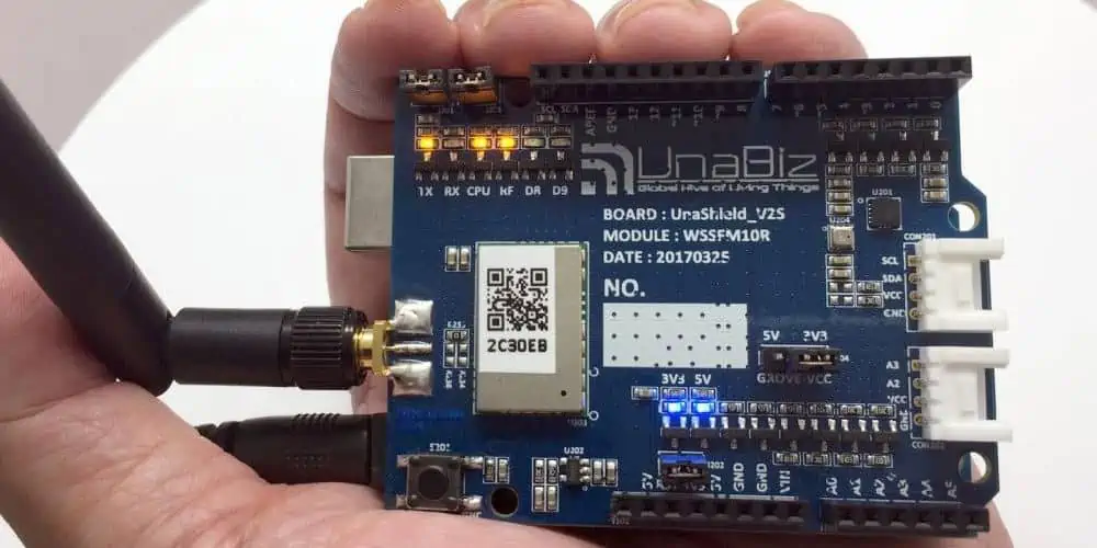
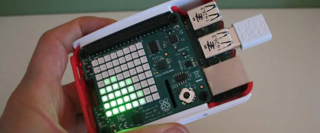
Big companies like AWS, IBM, and Microsoft have a specific way of explaining the IoTs. They say that you can use a small computer (like Raspberry Pi), a program (like Linux), and a wireless connection (like Bluetooth) to link up with services on the internet. 

Apple has a different way of explaining the Internet of Things. They say that if you have the Apple Watch, they will do the difficult work of connecting it to other devices and services. Think of a way you would like to use the Apple Watch. They will provide the operating system (watchOS), different ways of connecting to the internet, & tools to help you browse the internet. In other words, Apple is making it easier for people to create IoT solutions without worrying about the complicated parts.ย 

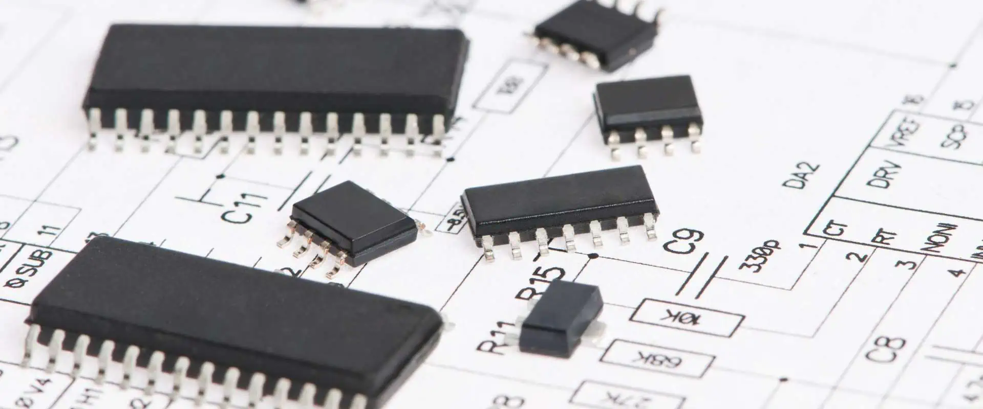
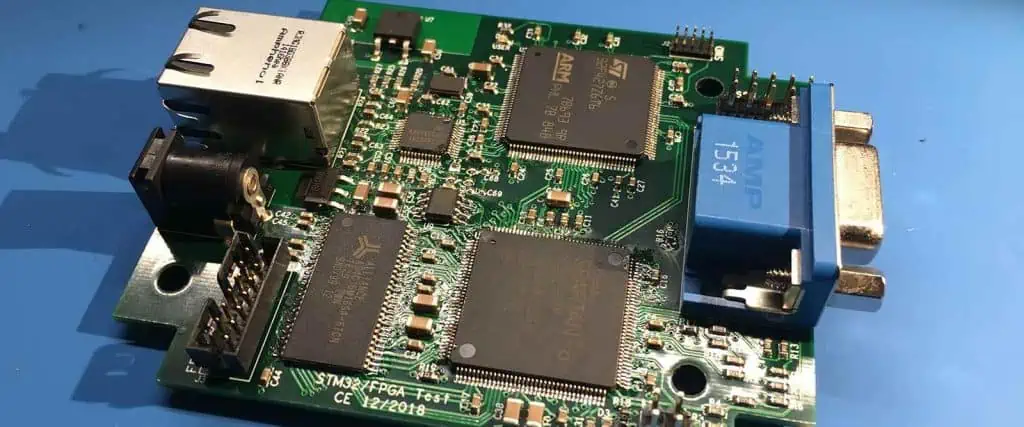
The Hardware Of Apple Iot

apple iot
apple iot

Apple has taken a consistent, slow, deliberate approach to its foray into the Internet of Things (IoT).

Apple’s strategy is to use one device as a “bridge” to connect to other devices. For example, the iPhone can relate to other applications using Wifi, Bluetooth & NFC. The first Apple Watch was made to work with the iPhone, and it had more features and was harder to use. 

Things are different now – the Apple digital watch can work independently and doesn’t need another device to connect to. It can act as a “bridge” itself. Two ways it does this are with Emergency SOS services and AirPods. The AirPods have become more competent and can connect wirelessly to the Apple digital watch, making it do more things. In the coming days, Apple and other companies will add more hardware to make the wireless feature of the watch even better. They may do this through the Programming toolkit. The Emergency SOS function demonstrates how the Apple Watch can link with cloud services using WatchOS.

Apple is making increasingly more smart devices that can connect to other devices. These new devices are going through similar changes that the iPhone underwent when it first came out.

As the iPhone evolved, it became a standalone appliance that could function independently.

The iPhone for the third generation acted as a tool that connected other devices.

In the 4th stage of the iPhone’s development, it no longer has to work as a connector for external devices. 

Apple’s appliances follow a similar pattern of change. Each change makes the device more complex, but it also creates new chances for creators to develop their add-ons and improvements.

Connecting Apple IoT Hardware with Software

FULL PCB MANUFACTURING Quote

To begin, Apple’s initial focus is on creating hardware that often surpasses the capabilities of the accompanying software. The newest iPad Pro is an excellent example of this. The operating system for a whole year did not support its advanced features. Fortunately, the Program can be regularly improved through updates, and Apple employs three distinct strategies to ensure optimal software performance.

  • Core OS
  • Cloud services
  • Connectivity

Most of Apple’s devices use a system called iOS. It has different versions, like tvOS, padOS, and watchOS. Regarding IoT (Internet of Things), iOS has many tools that can help. One of these tools is called HomeKit. It lets you control smart applications in your house, like lightbulbs, ovens, and air conditioners, from one place.

If your iPhone or iPad can’t do everything you want it to, you can use cloud services to make it better. Companies like Google, Amazon, and Microsoft offer tools that can help your iOS device do more things. These tools are called IoT services, and they work with your iOS device to make it even more powerful. 

When discussing making things work on our Apple devices, we must consider three essential things: software, services, and connectivity. While software and services help our devices do specific tasks, the connectivity makes it all work together. Apple devices can connect to lots of different things, and as a producer, you can use these connections to make your apps and services even better. 

  • All WiFi channels, including 6
  • Complete Bluetooth support
  • NFC (limited to credit cards)
  • 3G/4G
  • GPS

In short, Apple wants Programmers to have lots of options when it comes to connecting their apps and services. You can choose the services you need to make your app or service work best.ย 

Building Apple IoT Solutions with Devices

Apple gives you a starting point to create IoT solutions. It would be best if you used different devices to get started, such as

Here are some examples of the kinds of devices you can use with Apple to build IoT solutions:

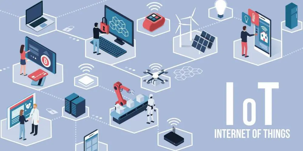
Smart homes: This includes things like lightbulbs, heating systems, power usage monitors, and security cameras.

  1. Health devices: You can use pedometers, weight scales, posture monitors, and glucose meters to track your health and fitness.
  2. Intelligent buildings: You can use Apple devices to control and monitor things such as temperature, lighting, and security in large buildings.
  3. Toys: Some toys can connect to Apple devices and provide new play and learning methods.
  4. Cars: You can connect your vehicle to your Apple device to get information about its performance or to control things such as the stereo or climate control. 

There are endless possibilities for the things you can do with Apple devices connected. 

Future of Apple IoT – Look at What Amazon is Doing.

It might sound surprising, but Amazon is helping shape the future of Apple in a lot of ways. It is the best at providing cloud services & they have a version of Android called FireOS that is used in tablets, TVs, and bright devices. They are also making it easier to connect devices. For example, the latest Echo devices can be connected to your home network in just one step by clicking on an Alexa application.

Apple is probably observing what works well for Amazon, such as their Echo device. It also monitors how Amazon tries new ways to engage with its customers, like its smart ovens. 

In the long run, everyone is focused on the goal – pleasing clients. Even major companies involved in IoT, such as Apple, have joined forces with the Zigbee Alliance to promote standardization in IoT.ย 

Want to Work in the Exhilarating Field of Apple IoT?

embedded iot

If you’re interested in starting a career in IoT, you can begin by taking Simplilearn’s training course called “Introduction to the Internet of Things.” However, IoT is present in almost all digital technologies. You can select to specialize in IoT as a Cloud Computing expert or analyze the vast Data amounts generated by the Internet of Things. The Internet of Things creates many job opportunities, and Simplilearn can help you start or advance your career with its learning paths. Check out their other resources to know more.

Apple IoT – A Pioneer 

Imagine that the IoT is a worldwide system for exchanging information, according to JCA-IoT. Its strength comes from linking physical & virtual things through compatible communication technologies. Based on these definitions, it’s clear that connected sensors are at the core of the IoT. 

Power of Connected Sensors

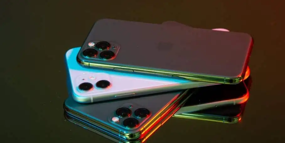
The iPhone, released in 2007, was the first widely used device to demonstrate the potential of linked sensors. Organizations such as Foursquare and Uber gathered a vast amount of data on people’s destinations and the times they went there via iPhone.

Most IoT applications meant for consumers operate using a smart application. Cell phone connection is also utilized in various industries. With an iPhone, it is possible to track things ranging from Oil derricks to the health of heart patients. A company called Airstrip has created a tool that lets doctors see important information about a pregnant woman & her baby, such as their heartbeats, in almost real-time. They can do this on the iPhone from anywhere in hospitals. That’s why four out of five doctors choose the iPhone over other smartphones. 

New Possibilities for Connectivity 

Apple created the first-ever smartphone called the iPhone, and it continues to make the best smartphones. They also created Apple digital watch, which has many sensors that can help with medical things. Organizations such as Airstrip can use these sensors to help with healthcare, just such as Foursquare helps find places for fun or shopping.

Apple makes all their products work well together without any problems. They make Apple Watches, iPhones, iPads, and MacBooks that all work together efficiently. It gives Apple a significant advantage over other companies. For example, even though IBM and Apple useful to be significant competitors, IBM chose the iPad to use with their super-smart computer Watson instead of a different kind of computer.

Public’s Imagination

ThroughTek was surveyed in 2015 and said that Apple was the most popular brand for IoT (Internet of Things). Even though some people think that Amazon or Google make more IoT products than Apple, they do not understand something important: Apple has inspired many people to create new kinds of connected products, like Uber.

The organization has become more popular among people than any other company. Have you ever seen an advertisement on TV for Fitbit? I haven’t seen one. What about an ad for the Apple digital watch?

Have you ever seen an ad where people wearing an Apple digital watch Series-two are running and swimming with ease and joy? These ads are so well-made that they stay in your mind, even if you only see them once or twice. The ad highlights that the Apple Watch Series 2 is waterproof.

Amazon is making amazing commercials for their device called Echo. The ads show a friendly helper Alexa who can turn on the sprinklers to make someone go away if they’re not wanted. However, Amazon still has much work to do to become as popular as Apple.

Some people don’t think the Apple digital Watch is as popular as the iPad or iPhone, which immediately became famous.ย 

Apple IoT New Possibilities for Healthcare

When more people start using a unique technology that lets doctors monitor their health from far away, that’s when things will change. For example, there could be a band for the Apple Watch that checks your blood pressure and a little device that grips your finger to check your blood oxygen levels. These gadgets would connect to the watch using Bluetooth.

You could also have the EKG that shows how your brain signals make your heartbeat. It would use three stickers on the chest and be wireless, so it can connect to your watch using Bluetooth. I used one of these devices in the hospital recently.

If there are many unique gadgets, doctors can keep an eye on patients who don’t need to be in the ICU but need a lot of attention. It saves money because the patients don’t have to stay in the hospital.

As the Apple Watch gets cheaper and the unique health gadgets also get more affordable, more people will start using them. Eventually, almost everyone will use them, just like how we all use smartphones today. 

Laying the Groundwork for a New World

Get ready for the future, where someone is always watching you – but instead of a scary Big Brother, it’s your excellent doctor or a computer that’s just as smart as your doctor. This system can take care of almost everything except for the tough cases, which still need the help of an expensive human doctor.

Top 10 Online Circuit Simulators – A Closer Look at Online Circuit Simulation

online circuit simulation

It is undeniable that millions of circuit boards are created every day in our modern, technologically evolved society. Furthermore, a single electronic machine may really employ anywhere from 10-50 electrical circuits with ease. This means that to meet the huge demand for circuit boards, millions of electrical components must be used.

But do users intend to invest their cash in expensive electrical parts when they’re still designing their circuits and making mistakes? On a larger scale, can we truly afford to use electronic components continuously throughout the first stages of creating a circuit board?

There’s no reason to worry, though, because the answer is already prepared. Circuit simulation in electronics. That is correct! The combination of these three tough phrases will save you from squandering your electronic components while creating a circuit for the first time. How? Let’s see, then.

What Is Electronic Online Circuit Simulation?

circuit simulation
circuit simulation

A mathematical description of a circuit is known as electronic circuit board simulation or electronic simulation. In plainer words, this represents the mathematical representation of circuits that electronic engineers create in order to comprehend their behavior as well as assess how well their constituent parts interact. Engineers end up saving both money and time because the circuit board simulation makes it simple to comprehend the circuit board without having to build it.

There are primarily three categories of electronics simulation:

  1. Analog Circuit Simulator
  2. Circuit Simulation in Digital
  3. Modeling of Mixed-Mode Circuits

Advantages Of Online Circuit Simulation

Naturally, when something has such high demand, it must have some benefits, isn’t that right? Let us make a list for you!

  1. The fact that SPICE, LTspice, and other circuit simulation programs are all available free for use makes them very accessible.
  2. It is now simple to modify the simulator’s models and general behavior. As a result, exploring the circuit’s constraints and potentialities through repeated stimulation iterations becomes effortless.
  3. Altering various input parameters, such as currents and voltages for the electronic circuit, has also grown rather simple, including modifying the amount of the simulation’s component parts.
  4. These electronic circuit simulators are quite useful since they contain instruments for evaluating power distribution networks and power distribution designs.
  5. Moreover, analog simulators make it simple to test memory-related durations and latencies of system memory and to examine the length of the changeover between each level of logic on a variety of grounds.

Top 10 Online Circuit Simulators For Electronics Projects

FULL PCB MANUFACTURING Quote

Here, we’ve looked at a few tools and methods that may be quite useful for locating the information you need in one place rather than scouring numerous sources, which can save you a ton of time. The top 10 online electronic circuit simulators, which are fairly well-liked by users and are among the greatest tools available, are listed below.

1. Circuits Cloud

It is a cloud-based educational program that is free to use and supports PHP and Linux. For students who want to learn about and create circuits, it is the perfect instrument. It provides both analog and digital components; the former group comprises junction devices, measuring instruments, and operational amplifiers; the latter category includes flip-flops, logic gates, multiplexers, and counters.

Students may use this simulator to carry out a number of tasks, including engaging with the flipping switches and logic circuits, altering the data input, and observing the changes in the output data for sequential approaches. Also, it may effectively disseminate information about the design process of logic circuits.

Users may access Circuits Cloud absolutely free of charge by either creating an account at the site or by logging in using their Google or Facebook accounts.

2. PartSim

PartSim is typically a web-based circuit simulator software that works much like an internet browser and offers simple tab navigation to access its components and probes. It features a straightforward interface and drag-and-drop component placement that works similarly to other tools. Moreover, a function of snap-click cabling and testing simulation is available for testing the samples.

A comprehensive Spice simulation system is included in the simulation capabilities, along with an internet-based schematic capture application and a graphic waveform reader that aid in keeping track of the digital and analog signal levels in the circuits. Last but not least, it is interconnected further with Dig-key BOM, allowing users to give parts numbers and subsequently search them by means of a distributor.

Users of PartSim have the choice of downloading a trial version for free without registering or joining the website.

3. CircuitLab

It’s an intriguing open-source program that lets users easily recreate their own ideas after sketching them out. It has intuitive digital or analog circuit simulation, expert schematic PDFs, and plots. They are non-installer-required and deliver all of these features.

The site’s distinctive features include special circuit URLs, which allow users to share their work and get online assistance, and additionally user-friendly formats that would let them enter values much like they would on sheet schematics. It also has a strong plotting engine, Smart Wires advanced technology, presentation-quality designs, and many other features.

The CircuitLab special Student Edition offers access to students upon the purchase of a school subscription, for which the universities or colleges must fork over a $2,400 annual site license charge. Going on the Mini edition is $24 annually, whereas the Hacker Life version is $79 annually.

4. DoCircuits

Comparison of measurement and simulation gain and noise figure (NF

DoCircuits, a user-friendly web-based simulation tool provided by Sparsh Technologies, is accessible through a web browser used by the user. The app’s three primary capabilities are creating a circuit, performing tests and statistics, and sharing ideas with the online community. Mostly on the virtual prototypes, the user must have the ability to drag the desired electronic component before using the click-to-connect feature to link them. Altering the layout after analyzing various aspects is another option.

Just the first of the tool’s three editions, called Hobbyist, Geek, and Hacker, offers without charge. There is a limit to the usage of 10 electronic components in each circuit board. Fifty simulations monthly, & 5 circuits on the cloud.

As you upgrade to the Hacker version ($2.99/month), you have access to limitless components. The features are 250 simulations each month, plus 50 circuits on the cloud. Last but not least, the Geek ($3.99/month) offers unrestricted access to all elements.

5. DC/AC Virtual Lab

For students as well as amateurs who like experimenting with circuits, this offers a realistic user interface. Users may easily create DC/AC circuits that include wires, resistors, and batteries, as well as other components, and afterward, compute the resistance and voltage. Moreover, it is useful to teach students interactively how to use a circuit breaker, test a capacitor, or locate a short circuit.

It takes into account the true performance of tools and parts, including illumination, burnout, and current flow. Finally, users have the opportunity to browse, share, and tweet generated circuits. Users can also simply design, simulate, and calibrate their circuits utilizing flexible wires. A software tool with an easy-to-use user experience. It has a quick simulation engine, DC or AC Virtual Lab.

The hobbyist, student, and school editions are available for $42, $84 (year), and $234 (annually), respectively, while the sample version is totally free. User registration is essential for all of the aforementioned publications on the site.

6. TINA

TINA is basically a software program that comes in the cloud as well as installable versions. It is useful for PCB designs and digital and analog circuit modeling. It’s strong and has a reasonable price for people who have grown familiar with circuits. It is capable of helping evaluate and build a broad range of circuits, including those for microcontrollers, MCU, VHDL, and optoelectronic applications. The fact that it works with the majority of gadgets and OS is another positive aspect.

Another feature is a lightning-fast multi-core engine. Another is a user-friendly schematic input that enables complex ERC functions useful to examine circuits for flaws. Moreover, it allows you to check your understanding, track your progress, and use troubleshooting methods.

Also, you may find the unknowable values for a number of parameters as well as create outstanding reports for schematic designs.

The website offers a variety of versions of this simulation model available in the cloud. The program is available in a variety of versions with a price starting at 129 Euros for various user groups.

7. Multisim

National Instruments’ MultiSim is a top-of-the-line SPICE simulation system that teaches students how to design, prototype, and test circuits in a realistic setting. Because of its methodology, you can store prototypes and improved PCB designs early in the whole process.

Users can pick from flexible layouts with more than 1400 pin layouts. This facility is available for even 4-sided PCBs. There are choices for design validation. There are two different versions; the first is free and has only the most basic functionality, whereas the second costs money and has features like increased integration from the schematic to evaluation and error minimization.

Although the trial edition is free, users must register on the site and then select a plan that best suits their needs in order to utilize the other editions intended for students, circuit designers, researchers, and educators.

8. 123D Circuits

The management of Components in PCB Layout and Design

For people who are eager to work at Arduino, this application by Auto Desk is just another free and open-source tool for circuit modeling. Users may use a mimicked Arduino circuit board and prototyping to build their customized virtual circuits. Also, users have the choice to incorporate LEDs into the project. It is testable to ensure proper operation afterward.

Resistors, potentiometers, capacitors, and oscilloscopes are just a few of the parts that may be used with this instrument. Moreover, you may utilize a variety of supported libraries of Arduino and code any type of Arduino code within the editor. The users may share their creations in real-time using a tool called collaborative editing.

It is a real-time online simulator, and there are no fees. People who want to utilize this simulator can create a free account.

9. PSIM

Powersim unveiled PSIM, a software program for simulating electronic circuits, in August of the previous year. Although it is to model power electronic devices and motor drives, any electrical circuit stimulates it. It provides a waveform analyzer and a schematic capturing interface.

It features many modules, including Processor-in-Loop, MagCoupler, Digital Control, ModCoupler, Motor Control Layout Suite, and SimCoupler. The intuitive and simple-to-use interface, extensive motor drive libraries, analysis of AC sweep, and quick simulation speed are some of the main advantages of this simulation program.

Its trial version is completely free. However, its student version, normal users, and professionals must complete an application and pay according to the plan they choose.

10. Spectre Circuit Simulator

Cadence Design Solutions’ Spectre is an electronic circuit simulator providing high-efficient and high-performance SPICE level RF and analog simulation. It offers an intuitive interface that effectively handles complicated analog or digital ICs, guaranteeing accuracy. Moreover, it provides precise post-layout simulation using lossy paired transmission wires and S-parameter modeling.

Enhanced statistical analysis, an interactive simulation configuration, post-processing of simulated data, cross-probing, and high-quality design are a few features of Spectre.

After registering on the Cadence website, users can access this simulator without paying any fees.

This collection of 10 online electronic circuit simulators is available to both professionals and amateurs who want to use internet resources for various electronic projects.

Exploring the Top Battery Eliminator Circuits

Battery Eliminator Circuits

The battery eliminator circuit is like a gadget that helps lower a big electric power to a small one. It is helpful for Contemporary remote-controlled aircraft, which use high-power batteries so that you can use the same battery to power all the different parts of the plane. There are many different kinds of these circuits to choose from. 

Do ESCs have Battery Eliminator Circuits

Yes! Many ESCs come with a built-in AC adapter. It means you do not have to worry much about powering your device. It would be best if you plugged the Battery Eliminator Circuit lead into the receiver, and it will provide the necessary power, usually 5 volts. However, for more powerful models, you may still need a dedicated Battery Eliminator Circuit.

ย Let’s look into this in more detail.ย 

(Linear) Battery Eliminator Circuits

Battery Eliminator
Battery Eliminator

A BEC reduces power, but it wastes a lot of energy while doing it. This energy turns into heat instead of being used. So, while a BEC is simple, it’s inefficient and uses valuable power.  

BECs cannot handle large batteries with increased voltages because it would make them too hot, and they would stop working. Electronics do not like heat. So, BECs can only be used for small things. 

(Switching) Battery Eliminator Circuits

A Switching Battery Eliminator Circuit is more advanced than a regular BEC and can power high-performance models. It uses a switching current to safely reduce the voltage to 5v for the RC gear, with very little wasted power. A capacitor and coil help to keep the voltage consistent for the Remote Control gear to run smoothly.

(Universal) Battery Eliminator Circuits

A UBEC is like a Switching Battery Eliminator Circuit. It also uses a switch-mode regulator to control the current/voltage for your important electronics. Different brands sometimes use UBEC/SBEC, but UBEC is becoming more commonly used as a common term. 

The Battery Eliminator Circuits

The BEC helps us make our electrically-powered models lighter. Most radio systems come with a heavy Nickel-cadmium battery with a capacity of 600mAh & four cells battery that weighs about 94 g. It is a lot for a beginner’s electric model like a Great Planes ElectriCub/Spectra. Although lightweight batteries are available, they are still too heavy for smaller & lighter models. The model can still fly, but it won’t fly as well. 

The BEC is a device that helps us get rid of the battery for the receiver. Instead, we can use the drive battery to power a radio system. However, this means there are some restrictions on where & how we should use the BEC.

How do Battery Eliminator Circuits Works?

FPC battery connector

The BEC is usually included in the ESC, which is responsible for controlling the speed of the motor. The BEC and ESC are separate parts, but they are available together by some wires and work together. Figure 1 displays the different parts of a power system and how they connect with an ESC with a BEC.

The BEC sends energy to a receiver using the same wire to control the motor’s speed. The receiver has three pins on each channel: plus, minus, & signal. We can use the plus & minus pins of any channel to provide power, and we don’t have to use the “Batt” connector on the receiver. Some small receivers designed for use with BECs do not even have the “Batt” connector.

It’s important to observe that the throttle and BEC parts of the ESC are together with the battery’s power wires. Even though they do similar tasks, they do them differently. 

The throttle manages the amount of power that goes to the motor. An electronic device called an “ESC” helps control the speed of a motor. It works by turning the power to the motor off and on quickly, many times every second. Modern ESCs do this around 1,500 to 3,000 times per second, while older ones do it around 50 times per second. The power amount the motor receives depends on how long the power is turned on. 

The BEC controls the amount of power that goes to the receiver & servos. The BEC has to keep a stable voltage to power the radio system. It has to maintain this voltage even when the motor battery voltage and servo loads vary. Also, the power supplied to the receiver must be free from electrical noise and voltage changes. It is a challenging task since the same battery that powers the motor is also the power(energy) source for the BEC. 

A Better Way?

You might have thought about how the throttle can deliver less power to a motor, even at higher currents, while the BEC can’t provide as much power or energy to that radio without overheating. The reason is off or on switching done by the throttle.

Instead of lowering the voltage, the throttle turns the full voltage on & off quickly to reduce power to the motor. The throttle doesn’t produce any heat. It does not dissipate power.

We can use a switching regulator to do the same thing for a Battery Eliminator Circuit voltage regulator. However, these circuits are usually large, heavy & expensive. Also, it’s challenging to design a switch-mode regulator that can provide clean power to the receiver without any issues. A linear regulator is cheaper and good enough for most purposes.ย 

Battery Eliminator Circuits Ratings

So we understand that a BEC’s performance is limited by its ability to dissipate heat, and the amount of heat it generates is proportional to the current and the difference between the input and output voltages; we can understand why most manufacturers specify the maximum no. of cells or servos that should/can be used with their Electronic Speed Controllers with BEC. 

If there are a lot of cells in the battery, the BEC needs more power to work. It means the voltage going into the BEC is higher. It widens the voltage gap between the input & the 5 Volt output. Also, using more servos leads to a higher current draw. 

Why should you use a Battery Eliminator Circuit?

It can be useful when you don’t have any batteries for your device. If your battery is broken or dead, the battery eliminator provides the necessary voltage to turn on your device using power from another device.

It can be useful when you don’t have batteries. It can supply the voltage needed to turn on your device using a different power source. You can also use it to figure out the precise voltage needed for your circuit without the hassle of constantly removing and replacing batteries. It saves time and effort. 

Maximizing Efficiency with RFID Modules โ€“ Uses & Applications

rfid module

The RC522 RFID Module is a device that reads and writes information using radio waves at a frequency of 13.56 MHz. It uses a special chip from NXP Organization called MFRC522. It’s a way of transferring data using radio waves. The RC522 RFID Reader/Writer Module can work with different types of RFID tags, such as cards and key fobs.

These tags have 1024 bytes of memory and work with a frequency of 13.56 MHz. The module is small, cheap, and doesn’t need a lot of power. It works with a communication protocol called SPI, which means it can easily connect to different microcontrollers like Arduino, Raspberry Pi, and more.

Examples of RFID module

RFID Board
RFID Board
  • Active tags: Some RFID tags have their power source and can send signals to the reader. It means they can work from far away, sometimes up to 100m or more, which is a lot more than regular smart card readers.

There are different types of RFID tags. One type, called BAP, has a power source letting it send a signal when an RFID reader is nearby.

RFID communication happens using different frequency ranges. Some are used to identify animals (120-150 kHz), while others are used for smart cards (13.56 MHz), and some can even be as high as the GHz range. 

NFC tags are small devices that use a specific frequency of 13.56 Mega Hertz. They can send information like credit card details, identification codes & other data. Some smartphones also have NFC technology built-in, so they can be used as either the sender or the receiver of the information. NFC tags allow phones with apps like Apple Pay to act like credit cards and enable “tap to transfer” facilities. This service connects two phones and then uses Wi-Fi or Bluetooth to transfer information. 

  • Passive tags: NFC tags get their power/energy from the active transmitter and then use some point to return the signal. Because they are designed to be passive, the power from the reader must be much more potent than the signals the NFC tag sends. Typically, the range of transmission is only some centimeters. Passive tags are often utilized to track items, which is what most people think of when they hear about RFID. You can also use passive tags on animals. These tags can be placed inside the animal or attached to them. It helps to locate lost pets or keep track of livestock.

Reader Module of RFID

The RC522 is a device that can read or write information from an RFID tag. It has three main parts:  approximately 27 Mega Hertz Oscillator, an Antenna, and MFRC522 IC.

  • MFRC522 Chip: It uses the Chip made by NXP Organization. This chip is to read RFID cards without needing to touch them, and it works using 13.56 Mega Hertz communication. The chip is a small, low budget, and uses little power to read & write information. The IC can work with different kinds of Tags, including MIFARE 4K, MIFARE 1K & MIFARE Mini, as well as other tags that use the ISO protocol. It can also communicate with Mifare series cards at high pace, more than 0.424 Mbps in both directions.
  • 27.12 Mega Hertz Oscillator: The small rock called quartz is used to help the computer keep time. The quartz vibrates very fast, about 27 million times per second. It allows the computer to know when to do things. Another smaller pulse of time, approximately 13.5 million times per second, from the first one by cutting it in half. 
  • Antenna: A tiny metal loop called the Coil is inside the small computer board. This loop sends out a particular energy wave that can make things happen. It works with other small things that don’t need their power.

Functioning Principle of RFID modules

FULL PCB MANUFACTURING Quote
  • RFID is a method that helps identify products without needing to see them directly between a small chip in the product (called a transponder) and a device that reads it.
  • RFID Structure always has two main parts. One is a small chip (transponder) that is attached to the product that needs to be identified. The other part is a device (called a reader) that reads information from the chip. The reader may only read or write a statement, depending on how the system is set up and what it’s meant to do. An RFID reader usually has four parts: an RF module, a control unit to set it up, a screen to show information, & an antenna to scan RFID tags. Some RFID readers can also send the information they collect to the other system, like a computer.
  • Tags โ€“ The central part of an RFID system that carries information is usually made up of two things: an antenna and a small electronic chip

Ten ways RFID module help your business

Radio Frequency Identification is a beneficial technology that can be useful in many different ways in business. It can help with things such as managing how to make things or checking equipment for repairs.

RFID technology can help businesses, no matter how big or small, become more efficient and save money, and make better use of resources. It’s beneficial for managing assets. It is an essential part of the IoTs. Following are ten ways RFID can be helpful.

1. Tracking assets 

For many organizations, it’s hard to keep track of all their stuff โ€“ such as parts on a production line and products being shipped out. But RFID technology can help by quickly and reliably keeping track of things without counting each item one by one. 

Using RFID technology, you can easily find out how many of a particular product you have and where they are, or what stage of the process they’re in. You can keep track of things from when they arrive in the store to when they’re useful in manufacturing. So this makes it simple to manage stock, check stock levels, and prevent theft. Radio Frequency Identification (RFID) can help you find lost things on the same site.

2. Saving time 

RFID technology can track the flow of goods automatically and send the information to financial management systems. It means you don’t have to fill out forms by hand or use old-fashioned spreadsheets. If you use fixed readers in essential places, it can save more time โ€“ for example, and it can eliminate the requirement for people to do things by hand. 

3. Improving data accuracy 

Since RFID technology collects and uploads data electronically, it avoids mistakes when people write things down, accidentally copy things twice, or forget to record items. When you use RFID to collect data on many items simultaneously, you can be sure you’re getting all the information you need. If you use cloud computing platforms, everyone in your organization can see the latest information about where things are or what’s happening to them. You can even share data with your customers.ย 

4. Enhancing health & safety

With RFID systems, companies can check when they last inspected equipment & vehicles and when they need to review them again. Tools like CheckedOK make it easy to manage reports & inspections and ensure that insurers and regulatory bodies are happy with the processes. 

5. Better control of production

RFID is great for production processes because it can identify individual items or parts. For example, it can ensure that specific molds are filled with the correct amount of liquids and cooked for the right amount of time or that certain parts end up in the right part of the production line. It can help cut down on waste and make things run more smoothly.ย 

6. Enhanced quality & traceability

RFID technology can ensure that things go through the correct checks & processes. It can ensure that a boiler is put together correctly, checked, and approved before it’s sent to the client. It can help make sure things are of good quality. Radio Frequency identification tagging can assist in keeping track of items from where they started to where they ended up. 

7. Increased revenues

By getting better at managing their inventory with RFID, organizations can offer services that make them stand out from the competition and make customers more satisfied. It can lead to more sales & better profits. 

8. More in-depth management information

RFID can collect data as it happens at various stages of an item’s life, which gives companies more information to help plan and make things run better. They can use this information to make things even more efficient.

9. Shorter processes

RFID can work together with other technologies used in manufacturing or supply chains, like automated systems for moving pallets and picking stock. RFID can make faster deliveries and shipments. 

10. Rapid payback time

RFID is an affordable technology. It saves money and extra income.

Applications of RFID module

RFID Antenna

Many different types of businesses also use Radio Frequency identification technology to do other jobs, such as

  • Asset tracking
  • Personnel tracking
  • Inventory management
  • ID badging
  • Supply chain management
  • Counterfeit forestalling

Radio Frequency identification technology has existed since World War 2, but the demand for Radio Frequency identification devices is increasing rapidly. It is due to the US Department of Defense & Walmart needing their givers to use RFID technology to track their products.

Radio Frequency identification technology is useful in various other things, such as:

  • Unlocking car doors
  • Automatic toll payment
  • Building entry systems
  • student Identification cards, Payment cards, and passports
  • Wireless sensors and mesh networks

If there is a need for RFID technology, applications that currently use barcode technology. It is to use RFID or a combination of both technologies. RFID technology has several advantages over barcode technology. One significant advantage is that the Radio Frequency identification tag can store more information about a product than a bar code can. Furthermore, Radio Frequency Identification tags aren’t susceptible to the problems that may occur with Scannable labels, like damage or becoming unreadable. 


How to Design PCB in EasyEDA

EasyEDA PCB

EasyEDA is a web-based software program that enables users to create PCB layouts and schematics for electronic circuits. Both experts and enthusiasts may use it because it should be simple. A schematic capture tool, PCB layout editor, and an integrated component library are just a few of the program’s many functions. Moreover, it has collaboration facilities that let numerous users collaborate on a project simultaneously. Electronic circuits, including analog, digital, and mixed-signal circuits, may be designed and simulated using EasyEDA. Due to its accessibility and ease of use, experts and enthusiasts favor it.

How does it work?

EasyEDA is a PCB layout and electronic circuit design tool that runs in the cloud. Users do not need to download or install software because it operates solely within a web browser.

Using tools like schematic capture, a PCB layout editor, and a library of components, users may build schematics and PCB layouts using EasyEDA’s user-friendly interface. Then, before the physical implementation, users may model and test their designs using the software’s simulation tool.

Users may work together on ideas and designs by sharing them with others. Ordering the PCBs and components required for the design is also made simple by EasyEDA’s interface with well-known providers like JLCPCB and LCSC.

Generally, EasyEDA is well-liked by experts and enthusiasts since it provides an easy-to-use method for designing electronic circuits and PCB layouts.

Steps of designing PCB in EasyEDA

EasyEda to KiCad

Here are the general steps for designing a PCB in EasyEDA:

Create a new project

The steps involved in starting a new project on EasyEDA are as follows:

Register for an account on the EasyEDA website or log in.

After logging in, you’ll move to the dashboard. Click the “Create a New Project” button.

Choose a category and give your project a name. For example, schematic software, PCB Layout, Simulation, Library, and Collaboration are offered categories.

If you wish to use a project template, you may also do so. For each category, there are several templates available.

After creating your project, you will move to the EasyEDA editor, where you may start designing.

You may expand your circuit’s component list in the schematic editor. Using the search bar, you may go through the categories or enter a single component’s name to narrow your search.

After you’ve located the part you need, click on it and drag it to where you want it to be in your schematic.

Use the “Wire” tool from the toolbar on the left-hand side of the editor to link components. You only need to click on one pin to begin the wire and another pin to end it.

You may arrange the components on the PCB and route the traces that will connect them in the PCB layout editor.

Further tools, such as “Design Manager” and “Library Manager,” are also available for managing design files and component libraries.

When complete, you may export and save your project in various formats, including Gerber files required for PCB manufacture.

Using the EasyEDA website, you may use the “Collaboration” option to share your project with others. This function may invite users to see and modify your project.

Import the .dxf Into EasyEDA

Hit the “New Lib” button after selecting “PCB Libs” from the top toolbar.

Give your library a name and choose “PCB” as the library type in the “New Library” dialog box. To create the library, click “OK.”

Choose the new library, then choose “DXF” from the dropdown menu by clicking the “Import” button on the top toolbar.

Click “Open” after selecting the.dxf file you wish to import.

Choose the appropriate import parameters in the “Import DXF File” dialog box. The measurement unit, the layer to import, the scale, and other settings are all selectable. Click “Import” when you have made your selections.

After the import is complete, the imported form should appear on the workspace. The form can then be adjusted as necessary using EasyEDA’s sketching tools.

Click the “Save” button after generating your unique shape to save your work.

Route and Allocate the Circuit Components

FULL PCB MANUFACTURING Quote

Make a schematic diagram of your circuit to start. EasyEDA offers a simple user interface for creating schematic diagrams using a variety of symbols and elements.

You may begin arranging the components on the PCB layout as soon as your schematic design is ready. Then, you may create the PCB layout for your circuit using the built-in PCB editor in EasyEDA.

Start by logically ordering the components on the PCB layout while considering component placement requirements, current flow, and signal pathways. Then, put related components in groups, and keep high-frequency components separate from those that produce noise.

You may begin routing the connections once the components are in place. Routing features from EasyEDA include manual routing, auto-routing, and interactive routing.

To reduce signal loss and interference, aim to make the signal pathways as short as feasible during routing. In addition, maintain as orderly and organized a routing as possible by avoiding intersecting signal pathways.

To examine your PCB layout for mistakes or violations, use the Design Rule Check (DRC) tool. For example, you can find any clearance violations, netlist mistakes, or overlap violations using the DRC tool.

If you are pleased with your PCB layout, you may create the Gerber files, which are the common files used by manufacturers to create PCBs.

To prevent losing any progress, always remember to save your work periodically. To get started and benefit from their program, EasyEDA offers many tutorials and guidance on their website.

Generate a netlist for the PCB layout

An essential step in designing a printed circuit board is producing a netlist for PCB layout. All of the design’s components, their connections, and the electrical connections that link them are in the netlist. The procedures to create a netlist for PCB layout are as follows:

Draw the schematic diagram for your PCB design using a schematic capture program. You must depict each component and its relationships in this diagram.

After drawing the schematic diagram, construct a netlist using the schematic capture tool. The components and their connections come from the schematic diagram in this procedure. It compiles a list of all the electrical connections in the design.

Ensure the netlist appropriately represents the schematic diagram after its generation. For example, you must review the netlist carefully to ensure all the components are available and their connections are proper,

Save the netlist as a file to load into the PCB layout software. The software stores netlist files in the SPICE, Protel, and PADS file

Import the netlist file into the PCB layout program. The physical arrangement of the components on the board and the electrical connections between them will be created by the PCB layout tool using the netlist.

Once the PCB layout is complete, you should run a design rule check (DRC) to ensure the design complies with all production limitations and specifications.

Lastly, producing a netlist is essential in creating a PCB layout. The netlist gives the PCB layout tool a direction to follow as it creates a physical layout of the board by precisely recording the electrical connections between the design’s components.

Design rules

easyeda 4 layer pcb

Observe these procedures to build up trace width, clearance, and through size design rules in EasyEDA:

Open EasyEDA and your PCB design project.

On the toolbar at the top of the screen, select the “Design Rules” button. The “Design Rule Check” (DRC) dialog box will appear.

In the DRC dialog box, you may specify your design criteria for trace width, clearance, and via size.

Click the “Net Width” option to adjust the trace width. You can provide a different width for each net or define the default trace width for all nets. We can also configure the minimum and maximum trace widths can.

Click the “Clearance” option to adjust the space between traces and pads. You can choose the minimal distance between traces, pads, and vias on various levels.

Click the “Via” tab to change the via size. You can specify different sizes for certain nets or set the default through size for all vias. Moreover, you may specify minimum and maximum through sizes.

You may also define other design criteria in the DRC dialog box, such as the minimum hole size and annular ring width.

Once you’ve established your design guidelines, save your modifications by clicking the “Save” button.

EasyEDA will automatically validate your design against the design guidelines when you work on your PCB layout. In addition, EasyEDA will send a warning message if you break any of the rules.

You can ensure that your PCB layout satisfies the requirements for your project and prevent mistakes and manufacturing problems by putting up your design rules in EasyEDA.

Copper pours

There are various advantages to using copper pours in your PCB design in EasyEDA:

The heat produced by PCB components may dissipate using copper pours. Therefore, you may lessen the chance of overheating and increase the dependability of your design by adding copper pours to locations with significant thermal loads.

Signal integrity can also improve via copper pours. Copper can lower noise and crosstalk in your design by giving return currents a low-impedance channel.

Copper can serve as an EMI barrier. As a result, you can lessen the possibility that your circuit will fail due to electromagnetic interference by enclosing delicate parts or traces in a copper pour.

Pours of copper can facilitate the production process. You may increase the effectiveness of the etching process and lower the possibility of mistakes by providing a sizable area of copper on the board.

Copper pours can enhance the overall appearance of your PCB design in addition to these advantages. Adding copper pours to any vacant spots may give the board a more polished and professional appearance.

It is easy to add copper pours with EasyEDA. You may construct a copper pour by using the “Copper Area” tool and drawing a polygon over the required area. Then, under the properties panel, you may modify the attributes of the copper pour, including the net association and clearing.

Design review

Hardware Layout
Hardware Layout

Check your PCB design for flaws like disconnected pins, design rule violations, or overlapping traces.

Use EasyEDA’s Design Rule Check (DRC) feature to verify your design for problems. The DRC tool can look for frequent mistakes, including overlapping components, trace width violations, and clearance violations.

Check the netlist to confirm the connections between the components. All components should connect correctly, and the netlist and schematic should match.

Examine the physical layout for flaws like overlapping components, incorrect trace spacing, or vias that are too near to one another.

Double-check the polarity of components, especially polarized components such as diodes and electrolytic capacitors.

Verify that the ground and power connections are free of mistakes. Verify that all power and ground connections are secure and that the power and ground planes are uninterrupted.

Check the footprints of the components to ensure they are the proper size and shape.

Check the bill of materials (BOM) to ensure all parts have the appropriate quantities and values.

If feasible, get a second pair of eyes to check your design for flaws. Often, we may find overlooked faults through a new perspective.

By checking it for faults, you may ensure that your PCB design is practical, dependable, and prepared for production.

Add SMT Assembly

After completing your design, select “Order PCB” from the toolbar at the top of the screen.

Click “Next” after choosing the necessary PCB amount and layer count.

Choose “SMT Assembly” under the “Assembly” menu, then pick the settings that best meet your needs. For example, if you want the EasyEDA team to manage every aspect of the assembly process, you may choose “Full Turnkey” or “Partial Turnkey” if you prefer to supply part of the components.

Click “Next” after making your selections, then enter your mailing address and credit card information.

Once you have reviewed the information for your order, click “Submit Order” to place it.

EasyEDA will start processing your PCB and assembly order as soon as you place it. Then, when your order is ready for shipping, you will receive an email notification.

Remember that EasyEDA provides through-hole assembly services, which one may choose on the “Assembly” page during ordering.

Advantages of using EasyEDA

Electronic engineers, amateurs, and students may design, test, and validate their electronic circuits fast and effectively with the help of this complete program. In addition, the software’s unique features, simplicity, and ease of use have helped it become more well-liked by users.

Integration with Other Tools

Users may easily import and export their designs because of EasyEDA’s integration with other tools. The software makes it simple to move designs across programs by supporting various file formats, including Altium, Eagle, and KiCad. Also, the program interfaces with widely used online storage platforms like Dropbox and Google Drive, making it simple to share and back up projects.

Low Cost

A less expensive option than other electrical design software is EasyEDA. We may complete little tasks using the program for free, and for more complex features, customers can switch to a premium subscription. The subscription plans are reasonably priced compared to comparable applications and provide outstanding value.

3D Visualization

Users of EasyEDA may see their PCB designs in 3D thanks to the program’s 3D visualization function. To help customers visualize how their design would appear in practice, the program creates a 3D model of the PCB. In addition, checking component placement and looking for potential design issues are possible uses for the 3D visualization function.

Simulation and Analysis

Users of EasyEDA may model and evaluate their circuits thanks to the program’s robust simulation engine. The program provides a variety of simulation models, including SPICE and Verilog, and supports both analog and digital simulations. In addition, users may easily comprehend and examine their circuits thanks to the graphical display of the simulation results.

Schematic Capture and PCB Design

Users of EasyEDA may create PCBs and schematics in the same piece of software. Program users may rapidly and effectively develop intricate schematics and PCBs thanks to the software’s complete range of capabilities. In addition, users can import pre-existing designs or start from scratch when designing their schematics and PCBs.

Large Component Library

Users may quickly locate the components they want for their designs thanks to the extensive library of components available in EasyEDA. Components, including resistors, capacitors, diodes, transistors, and ICs, are found in the library. Users can also design their own components or import components from other sources.

Collaborative Design

Real-time design collaboration is possible for users of EasyEDA. It is simple to exchange concepts and designs when several individuals work on the same project simultaneously. In addition, users may connect using the software’s built-in chat tool, making it simpler to debate changes, make improvement suggestions, and exchange expertise.

User-Friendly Interface

Users may easily move through the program because of EasyEDA’s simple user interface. All the tools and functions are readily available. The interface is straightforward, tidy, and simple. Users can add wires, drag and drop components, and construct their circuits. The program is suitable for educational and professional usage because it is suited for both novices and specialists.

Disadvantages of EasyEDA

Although EasyEDA provides many benefits, users should be aware of certain potential drawbacks. They consist of the following:

Limited Integration with Other Tools

While EasyEDA connects with other programs, some users might think the integration isn’t robust. For example, there may be restrictions on the quantity of data that may move between applications, or the program may not support all file types.

Privacy and Security Concerns

Users may worry about the security and privacy of their data as EasyEDA is cloud-based. Although the program has security safeguards like encryption and user authentication, some users may want to store their design data on a local computer or server for additional security.

Reliance on Internet Connectivity

EasyEDA requires an internet connection because it is a cloud-based application. As a result, the program’s performance may be impacted by slow or unstable internet access, possibly leading to data loss.

Steep Learning Curve

Although having a simple user interface, some users may find that it takes a while to get the hang of all of EasyEDA’s features and functionality. In addition, before they can use the software effectively, users with little to no expertise in electronic design software might need to learn the fundamentals.

Limited Functionality for Large Projects

Even though EasyEDA is a sophisticated program, it might not be appropriate for extensive and complicated applications. In addition, larger designs may be challenging for the program to manage because they are for small to medium-sized projects.

Limited Customization

Although EasyEDA includes a wide library of components, some users could discover that it is missing certain essential ones. In addition, although users can import bespoke components, there could be restrictions on how much we can customize the software.

Limited Offline Access

EasyEDA’s cloud-based nature, which necessitates an internet connection for users to access it, is one possible drawback. While this is practical for distant work and collaboration, it may provide issues for those who need to work offline.

Revolutionize Your Business with EDA Chip Design

eda chip design

EDA stands for Electronic Layout Automation, which is a group of software, Hardware & services that help in designing and producing electronic chips. It involves many steps, such as planning, designing, verifying, and manufacturing semiconductor devices. When it comes to making these devices, semiconductor foundries (also known as fabs) are the main givers of the service. These facilities are very complicated and expensive and are owned either by big semiconductor organizations or by independent manufacturing service providers. The latter type of service provider has become more popular in recent times. 

EDA solutions do not make chips, but they are essential in 3 ways. The EDA tools help in designing and validating the manufacturing process of semiconductors. This step is critical to ensure the performance and density of the chips meet the required standards. It is known as technology computer-aided layout or TCAD.

EDA tools are crucial in verifying that the design meets all the manufacturing requirements. If a design does not meet these requirements, it may cause the chip to malfunction or function with reduced capacity and pose reliability risks. Its role is called DFM.

The third way that EDA tools are used is to check the chip’s performance after manufacturing. It is done to make sure the chip works well from testing to when it is used in its field. The aim is to ensure the chip works as expected and is not tampered with. It is called silicon lifecycle management or SLM, a new area of focus. 

Semiconductor IP is a market that gives pre-designed circuits with different complexity that can be customized for a specific application. It allows for designing highly complex chips faster because previous can also be reused. Semiconductor IP is closely associated with the EDA market because it heavily relies on EDA applications. Because of this close relationship, the two markets often seem like one.ย 

How Does EDA Work?

eda chip
eda chip

EDA is mostly about software. It uses advanced and complicated software programs that mainly help design and make chips. 

  • Simulation tools are software programs that predict how the proposed circuit will work before being built. 
  • Design These tools help create a circuit by assembling different circuit components that perform a specific function. This process involves both logical and physical aspects. The logical part involves assembling and connecting the circuit elements, while the physical part involves creating structures that will be used to implement a circuit during manufacturing. These tools can be fully automated or require some human interaction to guide the process. 
  • Verification The examination of either the physical or logical representation of a chip is necessary to verify that the design/ layout is connected accurately and capable of delivering the expected performance. It is achievable through the use of various tools. 

Although Electronic Design Automation products are predominantly available in software form, there are instances where actual Hardware is useful to enhance their capabilities. This Hardware is useful when there is a need for high performance, such as processing large volumes of data during verification and simulation. A hardware prototype of a circuit typically outperforms a software application that runs the same model in all scenarios. This significant speed improvement is necessary to accomplish diverse tasks within a reasonable timeframe (hours to days instead of weeks to months). Emulation & rapid prototyping are the two primary methods for delivering EDA hardware. 

Types of EDA Tools

ยท Simulation

Simulation tools utilize a standard hardware description language like Verilog or VHDL to take a proposed circuit’s description and forecast its actions before implementation. These tools use diverse techniques to model the performance of circuit components at different levels of complexity and perform several operations to anticipate the circuit’s ultimate performance. The amount of detail necessary for a circuit’s design and its purpose determines the extent of input information needed. When dealing with vast amounts of data, hardware methods like emulation/rapid prototyping are useful. It is especially true when running a processor’s system against scenarios like video processing. So without hardware aid, the runtime for such situations can be impractical.

ยท Design

Design tools utilize a circuit function description to compile a set of circuit components that can execute the said function. This process involves a logical selection and interconnection of the appropriate circuit elements to achieve the desired outcome. Logic synthesis exemplifies this process, which can also take a physical form involving the assembly, placement, and routing of geometric structures that execute the circuitry in silicon, referred to as place & route. Additionally, the process can be interactive.

ยท Verification

To ensure the proper connectivity and required performance of the design, verification tools scrutinize either the physical or logical expression of a chip. Various processes are useful for this purpose. Physical verification, for instance, inspects the placement of interlinked geometries to make sure that they comply with the manufacturing specifications of the fab. The manufacturing requirements for physical verification have grown increasingly intricate, encompassing over 10,000 rules. Validation can also involve verifying whether the fabricated circuit accurately reflects the desired function by comparing it to the original description. An example of such a process is Layout vs. Schematic (LVS). Additionally, simulation technology can be useful for functional validation of the chip to compare its actual performance to the expected behavior. The effectiveness of these methods depends on the comprehensiveness of an input signal given. An alternative approach is to validate the circuit’s behavior algorithmically without necessitating an input signal. This technique, known as equivalence checking, falls under the umbrella of formal verification.

The History of EDA Chip Design

FULL PCB MANUFACTURING Quote

EDA originated in an in-house capacity. Before EDA became a target market, significant OEMs with vertically integrated operations had their own manufacturing capabilities and chip design. These entities maintained extensive teams of engineers that developed the necessary equipment for the automation of the layout, implementation & verification of their manufactured chips. The OEMs exclusively employed all chip creation for their product integration.

Texas Instruments, Bell Laboratories, Intel, General Electric, RCA, Sony, & Sharp are notable examples of such companies. The inception of EDA tools took place in three distinct phases. 

The initial phase, which commenced in year 1960s, witnessed the introduction of computer-based graphics design techniques for commercial purposes. These systems aim at various markets, such as mechanical design, architectural design, and cartography. Moreover, these systems were useful for the interactive layout of the circuit.

 During this phase, Calma, Applicon, and Computervision were the three key companies spearheading these developments. The GDS 2 version persisted as the standard format for conveying IC design information for many years. The CAD or CAM era characterized this stage of the industry. 

The 2nd phase of an EDA commenced in the 1980s, coinciding with the advent of the commercial ASIC industry. So the emergence of the ASIC industry makes custom chips. This development marked the inception of a semiconductor revolution, which continues to this day. LSI Logic & VLSI Technology were among the early ASIC companies. With the emergence of this advanced market, the demand for tools that automated the simulation, layout, and validation of the chips became much more prevalent. This phenomenon gave rise to several new companies that catered to this demand. The commercial EDA industry started to grow as many of the internal teams at large OEMs found fresh, lucrative, and stimulating opportunities in this emerging market. 

So here, the main emphasis was on software along with some special hardware for capturing the design description and simulating it. The three leading companies during the phase were Valid Logic, Mentor Graphics & Daisy Systems. It is CAE. 

During the 1980s, the industry entered its 3rd phase and underwent a period of maturation. So broad-line suppliers emerged, offering a range of software & hardware products to automate a greater portion of its Integrated Circuits design process. The phase by the emergence of the term electronic design automation was by three key players: Cadence, Synopsys, and Mentor (Siemens EDA). Even today, this era continues to resonate with many people in the industry, and the trio of top companies has remained unchanged.

As semiconductor technology continues to experience significant growth, there is a trend toward requiring a broader range of tools & technologies, which could indicate the onset of the industry’s next phase of evolution.

Why is EDA Chip Design Important?

EasyEDA-tutorial

The complexity of semiconductor chips is remarkable, with modern devices featuring upwards of one billion elements. These elements are capable of interacting with one another in nuanced ways, and any deviations in the production procedure can introduce further intricacies and alterations to their behavior. 

Sophisticated automation is essential for managing the immense complexity of modern semiconductor devices, and Electronic Design Automation (EDA) offers the necessary technology for this purpose. Without EDA, the design and production of contemporary semiconductors would be unfeasible. 

It’s important to recognize that errors in produced semiconductor chips can have disastrous consequences. Unlike software, you can’t fix chip errors through patching; there is a need to redesign and manufacture the whole chip again. This process can be both time-consuming and costly, often resulting in project failure. As a result, the high complexity of chip design requires flawless execution to avoid such setbacks. 

Meeting these challenges is impossible without the aid of EDA tools.

Challenges Faced By EDA Chip Designers

The challenges for chip designers are growing exponentially due to the smaller, faster, & more complex nature of chips. Fortunately, certain EDA equipment has been able to keep up with this trend. Additionally, some of the top tools have evolved into comprehensive software suites, alleviating design engineers’ concerns about compatibility between various tools. Below is a compilation of the typical difficulties that chip design engineers face and the effective tools and tactics that can aid in overcoming them.ย 

Challenge 1: EDA Chip Designers are struggling to connect Different software tools

It is common for chip designers to utilize multiple software tools for designing and simulating their devices. However, these tools often lack compatibility, requiring designers to create manual workarounds to facilitate communication between them. Furthermore, designers employ EM and circuit simulators, which are typically distinct from one another. As a result, designers conduct separate simulations using each tool and subsequently compare the resulting data. 

Designers are slow, and it affects the overall cycle. It is due to the time taken for importing, exporting, and error checking. 

Solution: Integrated Design Systems

Conducting circuit design analysis on many pieces of equipment can prove to be a time-consuming and challenging task. However, the good news is that there exist comprehensive design platforms that incorporate various libraries, design guides, bundles, and simulation components. Certain platforms even assert that they offer a complete suite of user-friendly 3D electromagnetic circuits & system simulators. Designers can conduct both EM & circuit co-simulation within a single tool. Advanced software tools are capable of integrating Circuit, layout and 3D EM components. Such tools can significantly enhance productivity and lower costs.ย 

Challenge 2: EDA Chip Designers Use Technologies at a rapid pace

jlcpcb impedance control

Currently, chip designers are confronting one of their most significant obstacles. The rapid pace of advancements and constant innovations are advantageous for semiconductor companies throughout the technology chain. The rise of digital wearables, sensors, & networking technologies is causing a surge in demand for Integrated circuits. In addition to this, there are emerging standards that require the consideration of more variables. As a result, semiconductor firms must continually innovate to promote connectivity throughout the technology chain. However, at present, engineers may not have the necessary skills to address this demand adequately. Therefore, developers must adopt advanced software tools.

Solution #1:  5G NR Technology

5G chipset manufacturers benefit from an early system modeling and prototyping platform that provides access to and integration of 5G NR baseband IP, different RF transceiver layout examples working in sub-6GHz & mmWave frequencies, as well as phased array and beamforming models that use radiation patterns from Electron Microscopy software. Proper waveform design and sophisticated RF and baseband system simulation are essential for the successful deployment of 5G technology

The Revolutionary Impact of NVIDIA IOT

NVIDIA IOT

It is a group of high-tech devices that developers use to make new AI products in different fields. Jetson is one of the best hardware platforms for Artificial Intelligence that you can use to learn about AI and do cool projects if you’re a student or a tech lover. The NVIDIA Jetson system has tiny but powerful computers called modules. The thing also includes JetPack SDK, which makes the software go faster, and a whole setup to help you create your own AI projects without any difficulty. The Jetson technology is high-speed and doesn’t use too much power. If you’re interested in creating AI-powered machines that operate on the edge, then it’s an excellent option. 

Jetson Platform and NVIDIA IOT

The NVIDIA Jetson system is liked by software developers, professionals, and students because it has many benefits. Some of the good things about it are:

Modular Flexibility: The Jetson system has different modules suitable for small businesses/large enterprises.ย The Jetson system has many modules, so you can find one that’s just right for your AI project, whether simple or complicated. The Jetson system also has a unified software system, which makes it easier for software developers to work with. It means they don’t have to keep rewriting code whenever they want to improve their inventions on different Jetson modules.ย The NVIDIA JetPack SDK has a Linux operating system, fast CUDA-X libraries, and tools that can help you work with various machine learning types, such as deep learning and computer vision. It can also work with different machine learning structures like TensorFlow and different machine vision APIs like OpenCV.ย 

NVIDIA IOT For Cloud-Native Technologies

NVIDIA IOT PCB Board

The NVIDIA Jetson system supports cloud-based technologies & workflows, such as orchestration & containerization, which help developers work quickly to create or improve AI products.  

Latest NVIDIA IOT Devices

Each NVIDIA Jetson is a self-contained unit package with its own GPU, CPU, high-speed connections, power management, memory, and other features. There are different types of Jetson devices available, each with varying levels of power efficiency, size, and performance so that they can be used in many various industries. The Jetson portfolio includes several different edge devices/modules.

NVIDIA IOT Jetson Nano NVIDIA

It is designed to help you add new features to small Artificial Intelligence systems. It’s great for developers or students just starting, as it’s designed to be hands-on and easy to learn from. Despite its small size, it is a powerful and energy-efficient module. It can handle complex AI workloads, process data from high-resolution sensors, and run many neural networks simultaneously. Because of this, it’s widely used for creating embedded Artificial Intelligence solutions & products. Its module is excellent for using AI to help computers see and understand images better. It can be used for tasks like identifying objects, separating parts of an image, detecting objects, and more. This tool works great with free programs that help computers see and learn, such as OpenCV. The Jetson to is a kit that developers find simple to use. That’s why both newbies and experienced developers use it with some cameras for Artificial Intelligence inference using deep learning. Its kit is excellent for experimenting & creating a prototype of a new AI solution.

NVIDIA IOT Jetson TX2 Series

FULL PCB MANUFACTURING Quote

The NVIDIA Jetson TX2 Series is a tiny but powerful module designed for efficiency & speed. It has the NVIDIA Pascal GPU, which is a type of computer chip that can process data very quickly. It also has a lot of memory and can connect to other devices easily. The Jetson TX2 can perform up to two and a half times better than the Jetson Nano but uses less power. Using the NVIDIA Jetson TX2 Series modules, you can run neural networks more accurately and efficiently on edge devices.

In the next part, we will discuss the variations among these devices. The NVIDIA Jetson TX2 NX, Jetson Nano & Jetson Xavier NX have the same size and shape. The other three modules, the original (accurate) Jetson TX2, Jetson TX2 4GB, and Jetson TX2i, are the same size as the original Jetson TX2. These modules are used in various fields like farming, healthcare, and retail. Out of the four components, the Jetson TX2i is designed to be tough. It can be used for high-performance Artificial Intelligence devices like medical equipment, industrial robots & computer vision cameras.

The rugged design makes it suitable for use in harsh environments. For instance, we have developed a livestock monitoring system that uses computer vision technology with the NVIDIA TX2. You can read the case study to know more. Edge computing tools are suitable for quickly processing data as it is being created. They can handle different temperatures, voltages, shocks & vibrations. Also, each device in the series has pre-loaded popular AI( Artificial Intelligence ) models, the NVIDIA JetPack SDK & NVIDIA Transfer Learning Toolkit.

Explore NVIDIA IOT in Embedded Computing

AI, which stands for Artificial Intelligence, is helping companies get ahead of their competitors in many ways. For example, it can automate tasks that used to be done by people, analyze large amounts of data to give businesses valuable information, and improve interactions with customers & employees.

NVIDIA Jetson is a popular platform used for making machines and other computer systems that can work by themselves. It has tiny, powerful computers called Jetson modules, software tools called JetPack SDK that help programs run faster, and a group of tools & products to help developers create things quickly. These tools include sensors, software development kits, and services to fasten the process. Jetson also works with that AI (Artificial Intelligence) software and computer techniques used on other NVIDIA infrastructures. It can help make machines that can work independently using software programs. Jetson is also very energy-efficient, which means it can use less power to do the job. It makes it an excellent tool for creating machines that can run using software programs.

Find Your Perfect NVIDIA IOT AI Computer

ยท For Product Development

No matter what kind of advanced product you want to create, like robots that can move independently, cameras that use AI to record video, or machines that can check things for errors in manufacturing, the Jetson family has something to help you. There are many options, depending on how much money you have to spend and how much power you need for your project. Jetson can work with various applications, so it’s an excellent choice for many projects. 

ยท For Educators, Students, & Enthusiasts

The NVIDIA Jetson Nano Developer Kit is perfect for people who want to learn about and create AI & robotics. It’s affordable but powerful, so you can get great results without spending too much money. This kit comes with all the software and tools you need to create amazing things using AI, just like professional developers do in many different industries. The Jetson Nano Developer Kit helps make AI & robotics reachable to everyone who wants to learn and create. 

ยท Scalable, Flexible Embedded Hardware Solutions

NVIDIA Jetson is a small computer with everything you need to start a project, including CPU, GPU, power management, memory, and High-performance interfaces. They come in different sizes and power levels and can be useful for all industries.ย ย Jetson ecosystem collaborators offer a variety of things to help you create your project, including software, help designing hardware, and products that work with Jetson. They have everything from simple parts to complete systems that can be used in many projects. By working with these partners, you can save time and get your AI-powered project ready to go more quickly.

NVIDIA IOT Create applications by the Internet of Things (IoT) and Artificial Intelligence (AI) 

NVIDIA Jetson Nano adds impressive new abilities to many small, energy-efficient machines using AI. It’s great for creating things like cameras and robots that are smarter and more helpful. You can use Jetson Nano to make intelligent devices that analyze video and make decisions. It’s also a perfect device to learn about AI & robotics.

ย Nvidia Jetson Nano vs. Raspberry Pi

  • Performance โ€“ Jetson Nano is more powerful than similar devices like Coral Board & Raspberry Pi with TPU. It has a better processor and memory, which means it can do more things simultaneously and work faster. Even if you are not using AI, Jetson Nano can run Linux appliances better than other devices.
  • Computer on SODIMM Card โ€“ The computer’s brain (CPU) and graphics card (GPU) are on a different board that connects to a slot on the central part of the computer where you plug things in. Nvidia also sells a more miniature computer called Jetson Nano with a lot of memory and storage.
  • Size and Weight โ€“ It is bigger than the biggest Pi 3B+, the Raspberry Pi. It needs more space because of the heat sink and the SODIMM slot. The Nvidia Jetson Nano board is 3.8 inches long and 3 inches wide and weighs 4.8 ounces, while the Pi 3B+ is only 3.4 x 2.3 inches & weighs 1.8 ounces.
  • Linux OS โ€“ The main computer program for a Jetson Nano and some Jetson boards is Linux4Tegra. It’s a particular version of Ubuntu 18.04 that works on Nvidia’s hardware. Raspberry Pi uses an operating system called Raspberry Pi OS (Raspbian), which is the main computer program we support for Raspberry Pi.
  • AI Experience โ€“ The Jetson Nano can do particular computer tasks related to AI, like recognizing objects, tracking movement, and making videos look smoother. It has a specific part called an Nvidia Maxwell 128 CUDA core GPU that’s good for artificial Intelligence. It can do 472 GFLOPS for Artificial Intelligence tasks, much faster than the 21.4 GFLOPS you receive with a Raspberry Pi 3B+.

NVIDIA IOT Expands Edge Tech for Robotics

Nvidia said at their conference in the fall of 2022 that they have some new updates, like a new infrastructure to make edge AI (a type of extraordinary computer work) faster and safer. 

The IGX infrastructure helps people and machines work together better in industries like manufacturing, logistics, and healthcare. It makes things safer in these industries because robots are useful more often.

Robots that help with tasks in factories and hospitals have an AI computer program. It allows the robots to know where things are so they don’t bump into people or things. Nvidia’s new infrastructure makes this safety property even better by using special sensors to detect problems before they happen. It helps keep workers safe.

โ€œJensen Huang, who is the CEO of Nvidia, says, “As people work more with robots, there are new rules to make sure everything is safe.” Nvidia IGX is going to help companies make new devices that are controllable by computer programs and can work safely around people. 

The safety features are changeable to fit different situations and reasons for using them.

Siemens is using Nvidia’s IGX platform to make their factories work independently. They’re using information from computers and digital models to teach robots how to work in warehouses. The robots will do tasks that people usually have to do repeatedly, which can be hard on the body. Siemens is the first company to use the IGX platform.

โ€œRainer Brehm, who is in charge of factory automation at Siemens, says, “They are working with Nvidia to make things happen faster with computers.” They want to use the IGX technology to help with tasks that people repeatedly do in factories. It will help the workers do their jobs better. By making the computers and machines work together more closely, they can help the factory be more efficient and change more quickly for the customers who use it.ย 

Benefits

The good things about the solutions from NVIDIA & Foundries.io are

  •    NVIDIA and Foundries.io have made it easier to make and use safe computers that work at the edge of networks. They use Jetson technology and JetPack to make it happen faster. Once you complete it, you won’t have to worry about updates for the rest of the product’s life. 
  •    NVIDIA and Foundries.io have made a safe Linux platform that you can use to build lots of IoT & Edge tools. You can make it work with Jetson technology and customize it to fit your needs.
  •    With the help of security features and updates that come over the air (OTA), you can ensure your devices stay safe. It’s easy to connect your devices to public/private clouds without worrying about security.
  •    You have the option to utilize containers for your applications & services. It lets you get OTA updates without needing to restart the device. It works with every Jetson product, including NVIDIA Jetson AGX Orinโ„ข.
  •    FoundriesFactory is an online service that helps product developers create, launch, and manage Linux software, apps, and services for Internet of things & Edge devices. You can use it for a long time, even up to 20 years or more.

What is 4G IoT? Most Common Cellular IoT Connectivity

4g iot

Wi-Fi, ZigBee, and Ethernet are just a few connectivity options for IoT networks. Nevertheless, among the most potent and flexible options is to utilize the current cellular networks by MNOs. The latest and most popular choice for IoT networks is 4G.

Even though 5G is now dominating the news, 4G continues to be a brilliant technology that is excellent for providing IoT connections for a wide range of applications.

In fact, according to statistics provided by ABI Research, over 60 percent of the total IoT devices use 4G technology. It continues to rule the IoT networking industry.

What Is 4G IoT?

The successor of 3G & 2G in terms of smartphone technology is 4G. Although 5G is still useful in places throughout the globe, 4G is practically the current generation in use.

Analog technology from the very first generation, known as 2G, lets users communicate while moving.

Calling and texting are possible by 2G, comprising data services such as SMS and MMS. Internet access and video chatting are two examples of far greater demanding data applications with 3G.

In comparison to 3G, 4G has a substantially higher user capacity. The 4G network provides mobile access to the internet to speed from a laptop or mobile device. It utilizes high-speed download data bundles. Usually speaking, 4G is three times as quick as 3G.

The key advantage of 4G is dependability, which is in addition to speed. It is far more dependable than 3G and allows for a higher traffic flow, which prevents congestion.

What Is 4G LTE?

embedded iot

The term 4G LTE is one that is frequently useful in relation to cellular network connection. While LTE really isn’t exactly similar to 4G, it has developed to function on 4G. LTE represents Long Term Evolution, a suite of technologies that are most frequently useful on 4G networks.

LTE is basically a modification of a 3G module. Its design includes an IP address-based core network, a streamlined network architecture, an advanced modulation technique, and a radio interface. It also permits the adoption of a method called MIMO. It makes use of many antennas to significantly improve data capacity.

LTE introduced an upgraded cellular network connectivity in 2008 with faster round-trip durations, improved spectrum efficiency, and higher data speeds. This is latency, and it usually lasts under 100 ms.

The theoretical maximum download speed for 4G LTE is 150 Mbps, although the usual download speed is 20 Mbps.

Any consumer of data network services can benefit greatly from the technology. However, the main advantage is the fact that it gives ready access to both consumers and users of industrial applications globally.

Long-term network continuity is provided by LTE while preceding 2G & 3G data networks are currently being phased out. Also, it serves as a link between these technologies alongside the more recent 5G. It won’t offer all-encompassing coverage for quite some time.

LTE and 4G IoT Categories

To ensure effective communication between the ground station and user equipment, LTE is classified into 20 distinct kinds of user equipment.

Categories 1 through 5 of what we can refer to as “original.” LTE offers downlink data speeds ranging from 10 to slightly under 300 Mbit/s. While categories 6, 7, & 8 are all thought to be a part of the recent LTE Advanced. The data rate for categories 6 & 7 is a little over 300 Mbit/s. But category 8 gives an almost ten times rise to 3000 Mbit/s.

Compared to conventional LTE, LTE Advanced provides faster speeds and better stability. Aggregating channels enable data users to download material from several sources at once, which results in these faster download rates.

There is additionally LTE-M, often known as Long Term Evolution CAT-M1. It is a much more straightforward variant of LTE created especially to function with rechargeable batteries IoT devices. It enables far high power-efficient data transmission and reception via cellular networks for these devices.

Example of 4G IoT

The fast data speeds, high dependability, low latency, and extensive availability that LTE offers many benefits.

One of them is the use of CCTV to offer oversight and security in places like airports and open areas like music halls. For mobile cameras like those on police cars, wearable body cameras, and drones, LTE connection becomes even more essential.

Applications utilizing autonomous guided vehicles in manufacturing facilities are further use cases that necessitate LTE’s low latency. If such AGVs ought to communicate their position promptly and precisely, low latency becomes crucial. Robots may transfer information into the cloud through the use of an IoT interface. It enables data analysis and coordination AGVs and robots.

4G IoT versus 5G LTE

FULL PCB MANUFACTURING Quote

Other than 4G, 5G is indeed the newest version of the wireless access network. It offers even greater possibilities for IoT devices and applications. 5G is evolving quickly. Speed is the primary distinction between 4G & 5G. Theoretically, 5G could travel at speeds that are 20 times speedier as compared to 4G LTE. Whereas 4G does have a top speed of one gigabit per sec, 5G might hit rates of roughly 20GB in one sec in the optimum conditions.

This is so that 5G, compared to 4G, may use substantially higher frequencies. Frequencies may be found in a spectrum between 6GHz and 54GHz, with the higher frequencies permitting several more simultaneous links than 4G.

The possible coverage is impactable by these frequencies. Longer ranges are possible with lower frequencies, although things like buildings and trees may block higher frequencies. This implies that IoT modules employing 5G placement must be properly thought out.

Moreover, 5G will have even reduced latency as compared to 4G. It is anticipated to decrease to about 10 ms, and under perfect circumstances, even 1 ms would be possible.

How Fast is 4G IoT?

Since it is generally accessible worldwide, it is excellent for business-based travelers and mobile data users. From specialist virtual smartphone network operators with international plans and connections, there are reasonable 4G LTE internet plans with international roaming options.

Business travelers do not have to rely solely on WIFI data connections because 4G LTE has upload rates of roughly 15 Mbps with downloading speeds of approximately 35 Mbps.

Also, compared to open and unsecured WIFI networks, their network connections are more secure.

Benefits Of Cellular 4G IoT For the Industry

IoT devices raspberry pi

ยท Large Coverage Area

Cellular IoT already has a wide coverage area since it leverages current mobile networks. This enables you to control the distribution of devices across several cities and nations. This is crucial for any Internet of Things program where data access is important, especially for applications like asset monitoring, transportation, and some other large-scale corporate software.

ยท Network-Switching 

M2M Prepaid SIM cards, in contrast to consumer SIMs, have the capacity to roam between providers with non-steered or steered open roaming. The cell phone will automatically join the network only with the strongest and clear signal nearby when using a non-steered Local sim card. This guarantees minimal downtime and continuous, dependable connectivity.

ยท Connectivity Choices 

Cellular IoT networks fall under a number of types, and you may choose the one that best suits your demands for data transfer. If your gadgets don’t carry large data loads such as video or demand continual connectivity and quick response times, it’s unnecessary to invest to choose the most costly plan.

ยท Remote Management & Analytics

With the help of IoT platforms, mobile IoT devices might be remotely manageabe. This enables the user to connect, detach, or troubleshoot mobile from any location. Users can track device usage, downtime, and other pertinent information with the correct IoT platform. It allows them to get the most out of the IoT application.

ยท Private Network And Security Options

Security measures are essential for every IoT application to guard against unrecognizable access. This is especially the case for a device that monitors sensitive data, such as medical equipment. Or for those that are vulnerable to criminal activity, such as smart city advanced technologies. Private network technologies like APNs, IPsec protocols, and VPNs may be used by cellular IoT systems. It provides security layers to the application, data, and network.

Types OF Cellular IoT Connection & Use

Arduino IOT

There are several network technology subcategories that cellular IoT connectivity might use. Depending on variables like cost, response times, and the volume of data, you may choose the best one for the particular use case.

ยท 2G & 3G

While 2G & 3G cellular networks are no longer useful for cell phones in industries, they are still in use for modern equipment, including vending machines and parking meters. Yet one limitation is that they are not able to transmit video.

ยท LTE Cat.0

There is Cat.0 supporting Iot networks with modest network requirements. It provides basic, constrained functionality at the lowest price. Wearable technology, alarm systems, and linked automobiles frequently make use of it. Japan, Australia, and the Americas all have extensive coverage.

ยท LTE Cat M

Compared to the previous version of Cat.0, the second generation LTE Cat M is considered highly efficient and effective. It features several power-saving features that are helpful in maintaining battery capacity and is among the most sophisticated connection kinds available on the present LTE infrastructure.

It’s important to note that LTE Cat-M allows greater rates of data and voice-over through the connection. However, it’s more costly than NB-IoT. This is because many latest IoT installations will take either NB-IoT or LTE Cat M connections into consideration.

ยท NB-IoT

4 Narrowband IoT, commonly known as NB-IoT, is a long-range, low-power, and incredibly dependable technology created exclusively for the Internet of Things. It uses 4G networks, however not LTE bands, to function, shielding it from interruption from other forms of connection and making it widely accessible in many nations. It does not, however, provide real-time communication as voice calls and does have some delay.

Having 685 million user connections anticipated to exist globally in the past couple of years, this sort of connectivity ranks as the fastest increasing.

ยท 4G LTE

The most recent cellular technology, 4G LTE, seems to be the preferred choice for networks with strong demand. Nevertheless, it is not particularly cost-effective and is probably excessive for Iot development with requirements that are less demanding than those of a smartphone.

ยท LTE Advanced

LTE Advanced becomes a quicker and more dependable variant of normal LTE that is used in applications that require the quickest reaction time, including autonomous cars.

ยท LTE-M And NB-IoT

iot-home-devices

Many connection methods assist in providing an excellent method, based on the device and app in question, because of the variety and various demands of linking IoT devices. The cellular sector is making investments in core technological variations in addition to the dominant GSM technologies to satisfy the requirements of IoT connection. They consist of the following:

ยท LTE-M 

LTM is “Long Term Evolution for Machines” LTE-M, one of the most cutting-edge connection options for IoT applications, and has a number of advantages, including data and voice support, a comparatively long lifespan of batteries, and low consumption of electricity. Mission-critical apps that demand high data capacity and rely on proper data transfer are better for LTE-M connections. Self-driving automobiles, networked medical devices, and other instances. On the other hand, NB-IoT and other IoT connectivity technologies, such as LTE-M, are more costly.

ยท NB-IoT

It is an abbreviation of “Narrow Band – IoT.” It is a type of IoT technology specifically intended for low-data, low-power applications. NB-IoT has advantages, including low battery consumption, extended range, and dependable connection, and is comparable with 4G devices. The amount of networks globally is anticipated to rise to 685 million in a couple of years, making it one of the IoT device connection technologies with the quickest rate of growth.

For IoT networks that don’t need a lot of bandwidth and simply transport small quantities of data, NB-IoT links are establishable. For usage in linked energy meters in smart cities and soil sensors in agriculture, for instance. Environmental sensors, which measure information about wind pressure and weather conditions but only communicate sporadically, are another use. The technology is useful for IoT applications that typically function from a specific spot and have a battery life of as long as ten years.

Why Choose RayPCB For 4G IoT Solutions?

RayPCB will be the best option if you need comprehensive, end-to-end mobile IoT enablement. We provide a variety of IoT solutions to meet the requirements of any application. You can quickly develop apps that can gather, analyze, and visualize your IoT cellular data in real time from any location in the globe.

RayPCB provides the proper technologies to increase your company’s business productivity and support revenue development thanks to our vast worldwide reach and client network. With RayPCB, worldwide IoT solutions may scale from just a few hundred to ten and even millions of linked devices while maintaining secure device connectivity.

STM32 PDB Design: Unlocking the Possibilities of Creative Design

STM32 PDB Design

The STM32 is indeed a development board with outstanding performance and a ton of functionality in a compact design. It contains a 32-bit ARM Cortex M3 CPU, flash storage of 64Kbytes, and SRAM of 20 Kbytes, all operating at 72MHz. It offers a wide variety of peripherals and I/O, including one PWM stopwatch, many high-resolution ADC, and multi-channel DMA. Also, it features several communication interfaces, such as USB, three UARTs, two I2Cs, and two SPIs. Moreover, it allows the board to be soldered with SPI Flash and enables the installation of more flash.

Features of Stm32 PCB Design

  • You can provide the circuit power source and USB connection using the onboard Micro USB interface.
  • LED test indication on board
  • Integrated power LED and reset button
  • Onboard 3.3V 100ma Regulator
  • The ids of all pins are indicated, and GPIOs are brought out.
  • You may immediately insert the circuit over the breadboard after the headers’ soldering.

Do you need a detailed manual for coding STM32 microcontrollers? In that case, you’ve found the proper site! STM32 microcontrollers know for their cutting-edge features, adaptability, and affordability. We will outline a step-by-step procedure for programming an STM32 microcontroller in this article. Also, we will go through the advantages of utilizing STM32 microcontrollers, their coding fundamentals, programming hints, and typical programming problems. Eventually, we’ll provide you with a few courses to support your beginning. So let’s start right now!

ย What is An Stm32 PCB Design Microcontroller?

STM32 PCB design
STM32 PCB design

Let’s start by providing a definition for an STM32 microcontroller. STMicroelectronics produces a particular kind of microprocessor known as an STM32 microcontroller. It is constructed using the 32-bit ARM Cortex-M CPU. Automotive, medical, consumer, and industrial electronics are just a few of the industries that utilize STM32 microcontrollers. They possess the feature like cutting-edge features, adaptability, and affordability.

STM32 microcontrollers have the ARM Cortex-M microprocessor in addition to other cutting-edge capabilities like

  • Several peripheral devices, including timers, analog-to-digital converters, and communication interfaces.
  • A large array of tools for software development that simplify programming.
  • Low consumption of power
  • enhanced performance.

STM32 microcontrollers are a great option for many applications because of their qualities.

Benefits of Using Stm32 PCB Design Microcontrollers

Let’s talk about the advantages of utilizing STM32 microcontrollers as you are aware of what they are. The affordability of STM32 microcontrollers constitutes one of their main advantages. They may be utilized in many different applications and are significantly less expensive than some other microcontrollers.

STM32 microcontrollers are inexpensive and offer a variety of software and peripherals development tools. They may thus be easily customized and are quite adaptable. They are also suitable for battery-powered devices due to their low consumption of power. The high-speed functionality of STM32 microcontrollers also qualifies them for devices that need quick processing.

Examples Of Programming Stm32 PCB Design Microcontroller

FULL PCB MANUFACTURING Quote

Required Tools

  • Breadboard
  • STM32 Development Board
  • STM32VubeMX, Support Pack
  • ST-Link Downloader
  • Keil5
  • Dupont Line

Procedure for Stm32 PCB Design

One # step: Connect The Dev Board To Your Computer

The proper STM32 development circuit board must be chosen for your program during the initial stage. Use the ST-LINK downloader to connect the board to the computer. You have to take into account elements like size, price, features, and performance. STM32f051k8u6 is a supposed example.

Two# Step: Download STM32CubeMx And Kiel5 Tool Kits

Visit ST’s official website or the Link below to download the “STM32CubeMX” program.

https://www.st.com/en/development-tools/stm32cubemx.html

Three # Step: Create A New Project In A STM32CubeMx

  • Click twice to launch “STM32CubeMX.”
  • Choose “New Project” from the menu
  • Using the MCU Filters, Then choose the desired board or MCU

Four # Step: Install New Libraries For STM32 Development Board

  • Download the stm32f051k8u6 library by selecting “Help then Install New Libraries
  • After downloading, choose “stm32f0,” and then click the button “Install Now.” The box becomes green.

Five # Step: Generate The Code And Save The Project

The act of producing C or C++ code entails creating the microcontroller’s instructions. An Integrated Development Environment (IDE) like IAR, Keil, or Eclipse is used for this. Of course, another option is to create the code using STM32CubeMX. 

Save the task:

  1. Type the name of the project into the “Project Name” field
  2. Choose the project and then save it to the “Browse” disk directory;
  3. Choose to produce the “Toolchain / IDE -> MDK-ARM V5” software project for Keil5;
  4. Create the project and choose “OK.”

Six # Step: Compile the Program Code In Keil5

After writing the code, it has to be compiled. The process of putting the code together into a type of format that the microcontroller can read is known as compilation. Here, the procedure is completed using Keil software. We first click “Open Project” to access the STM project we saved in the previous step:

Next, select “build” or hit the “F7” key to finish the project compilation.

Seven # Step: Debug The Program Code With Vision Debugger

The Keil5 Visionยฎ Debugger is used for debugging the STM32 development board’s program code. It offers an array of test features, including “Event Statistics,” “Execution Timing,” “Performance Analyzer,” “Event Recorder,” and “Component Viewer.”

Eight # Step: Upload The Program Code To The STM32f051k8u6 Dev Board

To finish the programming, click the button “Download” or hit “F8” on the keyboard.

Tips for Programming Stm32 PCB Design Microcontrollers

After acquiring programming skills for the STM32 microcontroller, let’s explore some programming tips. One key recommendation is to utilize the STM32CubeMX tool, which facilitates microcontroller configuration, code writing, debugging, and code uploading.

Another tip is to implement a control system to streamline the tracking of code revisions and ensure their up-to-date status. Additionally, it is critical to perform comprehensive testing of the code before uploading. This practice will allow the detection of any errors and guarantee that the code performs as anticipated.

Common Programming Issues

Debugging can prove to be a challenging task as it demands ample patience and a great deal of experimentation. It is crucial to utilize the debugger that is compatible with an STM32 microcontroller & conduct thorough testing of your code before uploading it.

Memory allocation stands as another prevalent concern when it comes to microcontrollers. It is the act of assigning memory to a microcontroller, which can prove challenging as it necessitates ensuring that there is sufficient memory available for both the code & data. Employing memory allocation equipment can be beneficial in facilitating the correct allocation of memory.

Comparison of Stm32 PCB Design with ATmega328

Having experience working with AVR-based microcontrollers such as the ATmega328, it’s more convenient to draw comparisons with the STM32. STM32 microcontrollers are generally more expensive than the ATmega328; they boast significantly higher memory & RAM. Additionally, the STM32 provides a wide range of chips, from low-cost options to more influential ones. With increased memory & storage, developers have greater flexibility in making applications and can expect faster operating speeds.

STM32 has another noteworthy advantage in the form of its abundant GPIOs and peripheral support. It supports various communication protocols, such as LIN, I2C, USB, I2S, SAI, IrDA, and many more. Furthermore, STM32 is extensively utilized in devices, particularly smartphones, tablets, and smartwatches. Leading tech giants, including Apple, Qualcomm, Nvidia, and Samsung, have adopted the STM32 as the foundation for their products.

Migrating from Arduino to Stm32 PCB Design Microcontrollers

Hardware Layout
Hardware Layout

Although Arduino is an excellent platform for gaining proficiency in electronics and creating preliminary prototypes, it’s usually impractical for some commercial products. If you want to know how to transition from an Arduino to an STM32 microcontroller, learn about the necessary steps.

Arduino’s platform has significantly reduced the obstacle to entry for hobbyists & startups to create their embedded devices.

The wide variety of production boards, straightforward programming & uploading interface, and expansive community support make Arduino an appealing first choice for product developers.

As project requirements expand and evolve with time, an Arduino platform may start to impose limitations.

One of the main factors contributing to this limitation is the narrow range of available hardware options, which is due to the substantial effort needed to seamlessly integrate the commercial microcontroller with the Arduino software.

Most Arduino microcontrollers utilize 8-bit AVR microchips, which have limited CPU performance capabilities. 

The performance drawbacks are amplified by the reality that the Arduino platform prioritizes portability and simplicity over fully optimized low-level configuration, resulting in much of the configuration being concealed from the user. As a result, software running on an Arduino is unlikely to be fully optimized.

Due to these factors and others, when there is a need to enhance the performance & flexibility of an embedded device, it’s typically necessary to transition away from the Arduino platform. Instead, a large proportion of industrial embedded systems employ 32-bit ARM chips, which power devices such as modern automobile computers & various others.

When it comes to balancing price and performance, there are no chips that can match these; the ARM processors have been a consistent feature of computing for a long time, with no indications of losing their popularity.

The STM32 series of microcontrollers is a highly sought-after alternative that preserves many of the attractive features of an Arduino platform. With the ability to reach CPU speeds of up to 550MHz and an extensive range of available chips, they unlock a vast array of new possibilities.

Conclusion

This blog post covers a comprehensive guide on programming STM32 microcontrollers. It encompasses the advantages of utilizing STM32 microcontrollers, fundamental concepts of programming them, suggestions for programming, and prevalent programming problems. Additionally, it covers the top development boards for STM32 microcontroller programming and suggests courses to initiate your learning journey.

A Complete Guide to ESP IoT Solutions and Modules

esp iot

In this blog, we will assist you in configuring the ESP-IoT-Solution development environment. Following that, a straightforward example will demonstrate how to set up a working environment, establish a project, compile and upload firmware onto the ESP32/ESP32-S series board, and do other tasks using ESP-IoT-Solution.

Introduction to ESP IoT Solution 

The following elements are mostly available in ESP-IoT-Solution, which may be useful as an additional part of ESP-IDF to enable easier development. It comprises code frameworks and peripheral drivers typically used within the Internet of things system development.

  • Device drivers for things like sensors, audio devices, screens, actuators, input devices, and more. Code structure and relevant documents for things like security encryption, minimum power management, storage, and other stuff. Entrance instructions for Espressif’s fully accessible solutions are out of view of actual use.

ESP IoT: ESP-32 or ESP-32-Sย 

esp iot PCB
esp iot PCB

To begin using the ESP-IoT-Solution, simply select a development board mainly from ESP32/ESP32-S family, or choose a supporting board straight from the Circuit Boards Component for a rapid start.

The following functionalities are supportable by ESP32/ESP32-S family SoCs:

  • Wifi at 2.4 GHz
  • Bluetooth
  • A powerful single-core or dual-core Processor that has the ability to operate at 240 MHz
  • Coprocessor with extremely low power
  • GPIO, I2S, I2C, SPI, UART, RMT, SDIO, LEDC PWM, TWAIยฎ, Ethernet, USB OTG, Touch, and other peripherals are among them.
  • Extensive memory resources, comprising external PSRAM compatibility and internal RAM of approximately 520 KB.
  • Support security features, such as hardware encryption.

The 40 nm-designed ESP32/ESP32-S line of SoCs exhibits the finest RF performance, power and adaptability, and dependability in a wide range of device and power settings.

ESP IoT Reduces Cost & Complexity Of IoT Devices

Nowadays, cloud connection is a hot topic, especially considering its many benefits, such as:

  • Enhanced device accessibility with Cloud connectivity;
  • Improved backup choices for important data;
  • Because of Over-The-Air updates, device security has been strengthened, and maintenance costs have decreased;
  • Enhanced productivity brought on by automation and enhanced device collaboration.

The technology is being extensively adopted across many industries thanks to these well-known benefits, to the point that almost 60% of organizations presently employ IoT, with just 9% of companies currently experiencing no IoT at all. IoT enthusiasts still face obstacles, which include the price of deployment and the incorporation of IoT using current technologies.

Espressif’s response to the IoT technology integration challenges and ensuing development expenses is ESP-Hosted. ESP-Hosted is an open-source approach that operates off-the-shelf, requiring little or very little modification to current technologies and reducing development expenses.

More specifically, ESP-Hosted provides a method for leveraging Espressif SoCs plus modules as telecommunication coprocessors. This approach gives the microcontroller, or host microprocessor, wireless connection like Bluetooth and wifi, enabling it to interface with some other devices. ESP-Hosted connects well with the host CPU via one of the widely used peripheral interfaces, such as UART, SDIO, or SPI.

FULL PCB MANUFACTURING Quote

The following benefits may be obtainable from this approach, which isolates the wireless connection module first from the primary host-processing module, by adding wireless capabilities to current MPU/MCU-based solutions:

ยท Faster Development Cycles

ESP-Hosted enables the connection module to operate over an 802.3 interface which is ESP-Hosted-NG, or the common 802.11 interface, which is ESP-Hosted-FG. In this manner, ESP-Hosted performs like a plug-and-play gadget.

ยท Reduced Re-Qualification

The bulk of a developer’s program does not need certification since installing the connection module doesn’t really affect user-space applications by ESP-Hosted.

ยท Power Saving

The primary MCU/MPU can continue to operate in a low-power state while still being interlinked with the network. As a result, only real activities, such as outsourcing all connecting overheads to a connecting module, require involvement from a main host.

ยท Easier Upgrades & Product Variants

Developers may create numerous iterations of an identical product with various connectivity options thanks to the design, which makes it simple to change the wireless connectivity of their goods. In the example below, the developer may utilize the very same Host programs and tools while choosing from a range of internet connectivity choices, including wifi 4, Wi-Fi-6, and Wi-Fi-6 dual.

To facilitate developers’ use of the numerous ESP32 functionalities, Espressif has developed the program code of the ESP-Hosted publicly available. Further useful to developers are the HMI and IO features of ESP32-S3 and ESP32, as well as the sophisticated security abilities of ESP32-C3 or the device’s Digital Signature Peripheral. As a result, the options are unlimited.

Variants Of ESP IoT

esp iot PCB
esp iot PCB

There are two versions of the ESP-Hosted solution: ESP-Hosted-NG and ESP-Hosted-FG. The kind of network interfaces given to the hosts and the configuration/control of wifi over the ESP SoC/module distinguish them from one another. Each variation has its own firmware software and host.

ยท ESP-Hosted-FG

This type gives the host a typical Ethernet interface of 802.3 standards. The following options are provided to the host so that they are able to do this:

  • a straightforward Ethernet interface of 802.3 standard, which is a network interface;
  • a simple control interface that helps in setting up wifi only on ESP SoC;
  • An HCI interface that is standard.

This method is perfect for all MCU hosts since it uses straightforward 802.3 interfaces. While utilizing this AT firmware-based method or when integrating the complicated 802.11 interfaces, the MCU program can keep taking advantage of the industry-standard TCP/IP stack as well as prevent substantial modifications to the host application.

ยท ESP-Hosted-NG

This variation adopts a conventional strategy while giving the host a type of network interface, making it especially intended for hosts that especially run the Linux OS. This enables the usage of ESP SoCs/modules with common wifi programs like wpa_supplicant. These benefits are provided by this answer:

  • a Linux host’s 802.11 standard network interface, a type of common wifi interface;
  • Under Linux, the cfg80211 standard interface is provided for wifi setup;
  • An HCI interface that is standard.

Features And Specifications of ESP IoT

ESP IoT Board
ESP IoT Board

1. Processors

As previously noted, the Tensilica 32-bit CPU powers the ESP32. This employs one or two cores. The performance is in the range of 600 DMIPS, and the frequency of the clock is over 240MHz. Also, even in a deep sleep state, its low-power use enables ADC conversions, calculation, and leveling of the threshold.

2. External SRAM

For the protection of developers’ software and data, ESP32 enables a maximum of 4 16MiB auxiliary SRAMs and QSPI flashes. The high-speed cache is used to access the exterior QSPI flash drive and SRAM.

3. Security

The security aspects of the IEEE 802.11 protocol, including WFA, WAPI, and WPA/WPA2, are supported. ESP32 also features a secured boot and storage encryption.

Functions of ESP IoT

Whenever it applies to the IoT, ESP32 has various uses. Just a few IoT uses for the chip include the following:

  • Networking: The module’s dual-core processor and wifi antenna allow integrated devices to communicate with routers and send data.
  • Data Processing: Processing simple inputs from digital and analog sensors to much more complicated calculations using a Non-OS SDK or RTOS.
  • Utilizing IoT P2P networking, direct communication is established between various ESPs as well as other devices.
  • Web Server: Access HTML- or development-language-written pages.

Applications of ESP IoT

The following are some major IoT devices frequently contain ESP32 modules:

  • Intelligent industrial equipment, such as PLCs.
  • Wearable health monitoring devices are among the smart medical equipment.
  • HVAC systems and thermostats are examples of smart energy gadgets.
  • Smart security equipment, such as smart locks and security cameras.

Chip Versus Module Versus Development Boards

The chip has no other name than ESP32. The format in which device makers and developers choose to purchase this is one of three options, and their choice will rely on the specifics of their situation:

ยท ESP32 Chip

Many Companies make this basic chip. It is unshielded and requires soldering to be connected to a board or a module. Because doing so would make the manufacturing process even more difficult, the majority of device makers do not merely buy chips.

ยท ESP32 Modules

The chip is housed in some type of surface-mountable module. The advantage of buying a module comprises that throughout the manufacturing process, they may be quickly installed onto an MCU. Device makers don’t have to worry about including extra steps in the process of production to meet FCC compliance in regard to wifi shielding.

ยท ESP32 Development Boards

The IoT Microcontroller development boards with modules already installed using the ESP32 chip. Before going into mass production, enthusiasts do the tests and prototypes of IoT devices, device makers, and developers. ESP32 microcontroller development boards come in a wide range of types and models from various vendors. While selecting an appropriate IoT ESP32 microcontroller development board, keep the following crucial specifications in mind: ADC pins, LEDs, shielding, wifi antenna, flash memory, and GPIO pins.

Best ESP IoT Module Or Development Board

embedded iot

There are many reasonable alternatives with ESP32 modules and boards, as the comparisons above demonstrate. We’ve included the most popular ones below to aid you in making a selection.

ยท ESP32-WROOM-32D

The ESP32-D0WD interacts with this ESP32 module that is quite popular. The ESP32-WROOM-32D’s flexibility is the major factor in its popularity. It may be useful for a range of applications, from voice compression as well as music streaming to sensor networks.

Mostly, ESP32-WROOM-32D and ESP32-WROOM 32U use wrongly in industry. Although the two modules are remarkably similar, the ESP32-WROOM-32U differs from the ESP32-WROOM-32D in that it incorporates a connection of U.FL.

ยท ESP32-WROOM-32

The initial ESP32 module released by Espressif is the ESP32-WROOM-32. A potent, general Wi-Fi+BLE+BT MCU device is the ESP32-WROOM-32. The chip ESP32-D0WDQ6 seems to be the heart of this device. Scalable and adaptable design features are available in the integrated chip. The ESP32-WROOM-32 is unquestionably a fantastic module, yet we do not suggest it for modern designs.

ยท ESP32-WROOVER

There are two variants of the ESP32-WROVER available; one includes a PCB antenna, while the other utilizes an IPEX antenna. The ordering details for both variants are available here. The ESP32-D0WDQ6 semiconductor, which is at the heart of this device, is similar to the ESPWROOM32 chip.

Two independently controllable CPU cores are present in this ESP32 device. The clock frequency of the CPU is changeable between 80-240 MHz. The user can also turn off the Processor and constantly check for alterations or threshold crossings using the less-power coprocessor.

ยท ESP32 CAM

In comparison with the various development boards here on the list, the ESP32 CAM seems to be a bit unique. An inbuilt camera with a miniature SD card slot is another feature of this properly developed microcontroller. As the ESP32-CAM has so far been based on the module of ESP32-S, it has similar features. This offers clock speeds that go up to around 160 MHz, wifi image uploading, 9 GPIO ports, I2C, SPI, and PWM interfaces.

It features a 2 Megapixel sensor-equipped OV2640 module which also accommodates OV7670 cameras. When exploring something like the ESP32-CAM, it can be simpler to forgo a solderless board due to the large number of components being placed on the bottom side. Also, we advise utilizing female Dupont connections with jumpers.