PCB Solder Pads Guide: BGA Pads, SMD Pads, Lifted Pad Repair & More

solder pad pcb

Introduction

In the world of printed circuit board (PCB) design and manufacturing, solder pads play a crucial role in ensuring proper component attachment and electrical connectivity. This comprehensive guide will delve into the intricacies of solder pads, covering everything from their basic definition to advanced repair techniques. Whether you’re a novice PCB designer or an experienced engineer, this article will provide valuable insights into the world of solder pads.

1. What Are Solder Pads?

Definition and Purpose

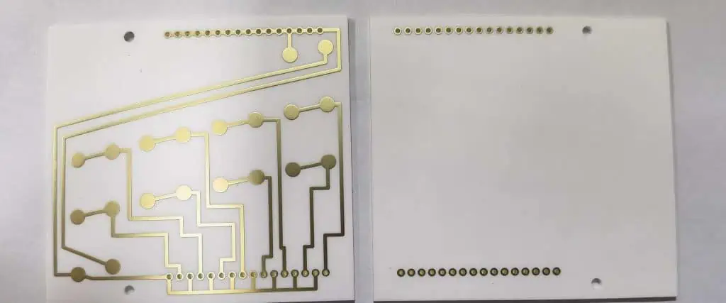
Solder pads are specially designed areas on a PCB where components are soldered to establish electrical and mechanical connections. These metallic surfaces serve as the interface between the circuit board and the electronic components, ensuring proper functionality and reliability of the entire assembly.

Anatomy of a Solder Pad

A typical solder pad consists of several layers:

  1. Copper layer: The base conductive material
  2. Nickel plating: Provides a barrier to prevent copper diffusion
  3. Gold plating: Protects the pad from oxidation and enhances solderability

Importance in PCB Assembly

Solder pads are critical for:

  1. Component placement accuracy
  2. Electrical conductivity
  3. Mechanical strength of connections
  4. Heat dissipation during soldering

2. Types of Solder Pads
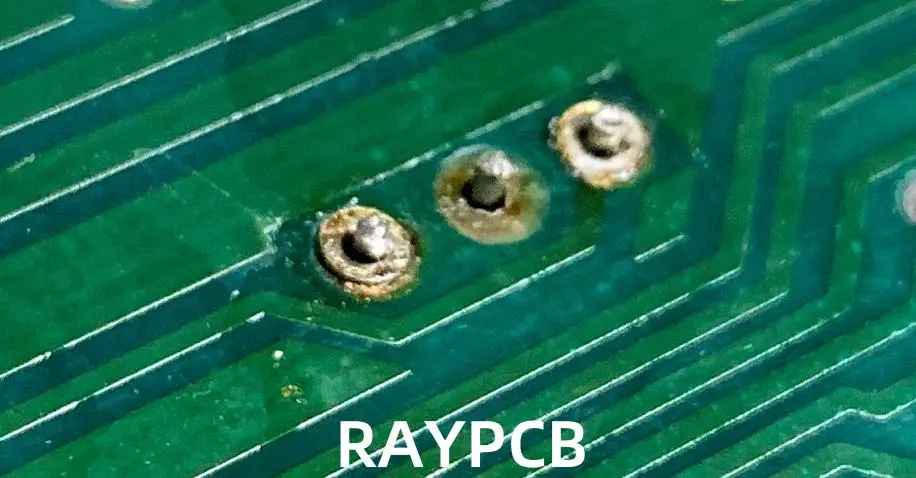
Through-Hole Pads

Through-hole pads are designed for components with leads that pass through the PCB. They feature:

  1. Circular or oval shape
  2. Plated through-holes
  3. Larger size compared to surface mount pads

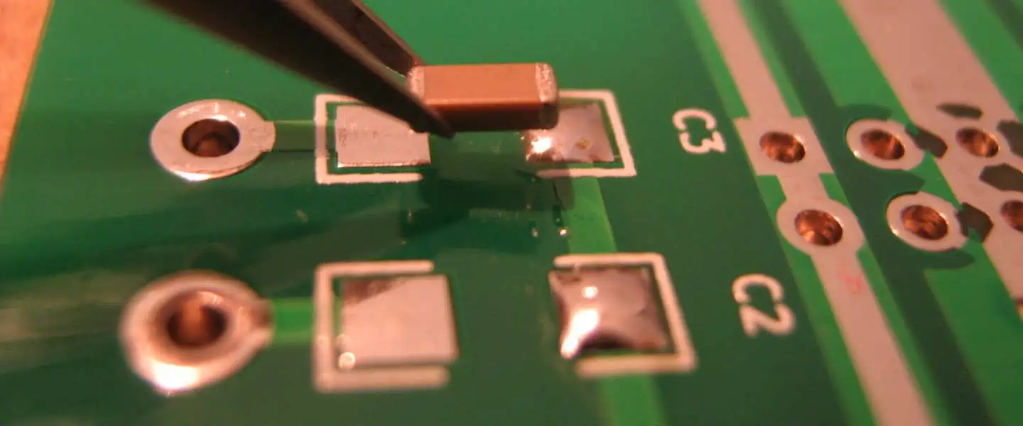
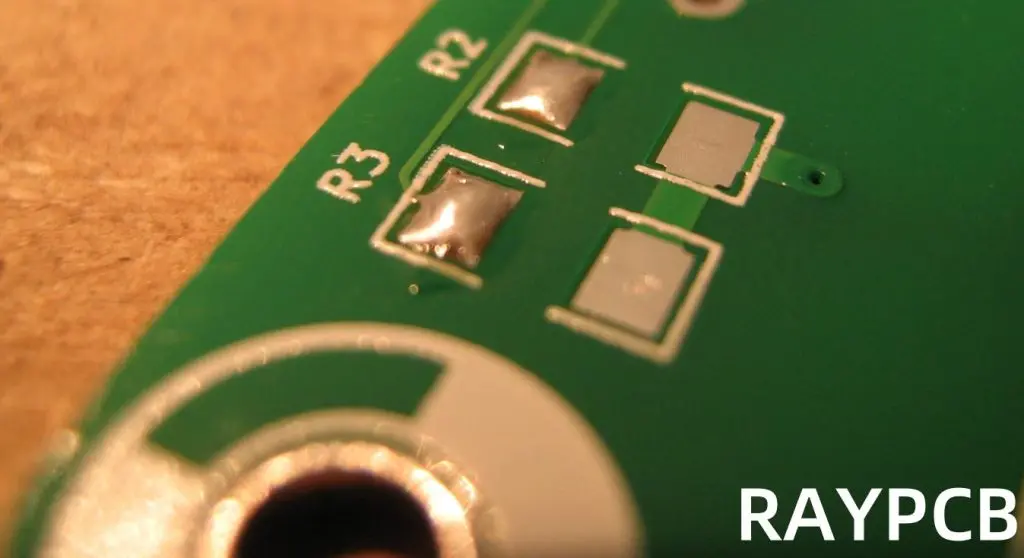
Surface Mount Device (SMD) Pads

SMD pads are used for surface-mounted components and come in various types:

  1. SOIC (Small Outline Integrated Circuit) pads
  2. QFP (Quad Flat Package) pads
  3. TQFP (Thin Quad Flat Package) pads
  4. SOT (Small Outline Transistor) pads

Ball Grid Array (BGA) Pads

BGA pads are designed for components with an array of solder balls on the bottom:

  1. Typically circular in shape
  2. Arranged in a grid pattern
  3. Require precise placement and soldering techniques

Castellated Pads

Castellated pads are semi-circular pads located on the edge of a PCB:

  1. Used for board-to-board connections
  2. Allow for vertical stacking of PCBs

Custom and Specialty Pads

Some applications require custom pad designs:

  1. RF and high-frequency pads
  2. High-power pads with thermal relief
  3. Fine-pitch pads for densely packed components

Read more about:

3. What Factors Dictate the Size of Pads in PCB?

Component Requirements

  1. Lead size and shape
  2. Package dimensions
  3. Pitch (distance between leads)

PCB Manufacturing Capabilities

  1. Minimum trace width and spacing
  2. Drilling and plating tolerances
  3. Solder mask registration accuracy

Electrical Considerations

  1. Current-carrying capacity
  2. Impedance control requirements
  3. Signal integrity concerns

Thermal Management

  1. Heat dissipation needs
  2. Thermal relief design
  3. Power handling capabilities

Assembly Process

  1. Soldering method (wave, reflow, hand soldering)
  2. Pick-and-place machine accuracy
  3. Rework considerations

4. Solder Pads Design Layout Guidelines

General Design Principles

  1. Follow manufacturer’s recommended footprints
  2. Consider thermal relief for large pads
  3. Maintain consistent pad sizes for similar components

Pad-to-Trace Connections

  1. Use teardrop connections for improved strength
  2. Ensure proper trace width for current capacity
  3. Avoid 90-degree angles in trace routing

Spacing and Clearance

  1. Maintain adequate spacing between pads
  2. Consider component body clearance
  3. Allow for solder mask and silkscreen clearances

BGA Pad Design

  1. Use non-solder mask defined (NSMD) pads for better reliability
  2. Implement proper via-in-pad design when necessary
  3. Consider dog-bone fanout for easier inspection and rework

High-Speed and RF Considerations

  1. Minimize pad size to reduce parasitic capacitance
  2. Use ground planes and controlled impedance techniques
  3. Consider coplanar waveguide structures for RF circuits

5. How to Fix Broken Solder Pads โ€” Tools and Steps

Tools Required

  1. Soldering iron with temperature control
  2. Desoldering braid or solder sucker
  3. Flux pen or liquid flux
  4. Precision tweezers
  5. Magnifying glass or microscope
  6. Isopropyl alcohol for cleaning

Step-by-Step Repair Process

  1. Assess the Damage
    • Determine the extent of pad damage
    • Identify any lifted traces or delamination
  2. Clean the Area
    • Remove any residual solder using desoldering braid
    • Clean with isopropyl alcohol to remove flux and debris
  3. Prepare the Surface
    • Gently scrape away any solder mask around the damaged area
    • Expose a small section of the trace leading to the pad
  4. Apply Adhesive (if necessary)
    • For severely damaged pads, apply a small amount of epoxy to secure the area
    • Allow the adhesive to cure completely
  5. Create a New Pad
    • Cut a small piece of copper foil to match the original pad size
    • Tin the exposed trace with a small amount of solder
    • Carefully solder the copper foil to the exposed trace
  6. Secure and Shape the New Pad
    • Use the soldering iron to shape the new pad to match the original
    • Ensure a smooth, even surface for component attachment
  7. Test Continuity
    • Use a multimeter to verify electrical continuity
    • Check for any shorts to adjacent pads or traces
  8. Apply Conformal Coating (optional)
    • For added protection, apply a thin layer of conformal coating
    • Allow the coating to cure completely before use

6. How to Clean a Solder Pad

Importance of Clean Solder Pads

  1. Ensures proper solder adhesion
  2. Prevents contamination-related defects
  3. Improves overall reliability of connections

Cleaning Methods

Mechanical Cleaning

  1. Use a fiberglass brush for light oxidation
  2. Apply gentle pressure to avoid damaging the pad
  3. Suitable for small-scale cleaning tasks

Chemical Cleaning

  1. Isopropyl alcohol (IPA) for general cleaning
  2. Specialized PCB cleaners for stubborn residues
  3. Always follow manufacturer’s recommendations

Ultrasonic Cleaning

  1. Effective for batch cleaning of PCBs
  2. Uses high-frequency sound waves in a cleaning solution
  3. Ideal for removing flux residues and fine particles

Cleaning Process

  1. Remove Excess Solder
    • Use desoldering braid or a solder sucker
    • Ensure all old solder is removed from the pad
  2. Apply Cleaning Solution
    • Use IPA or a specialized PCB cleaner
    • Apply with a lint-free cloth or brush
  3. Scrub Gently
    • Use a soft-bristled brush for stubborn residues
    • Be careful not to damage the pad or surrounding areas
  4. Rinse and Dry
    • For chemical cleaners, rinse with deionized water
    • Dry thoroughly with compressed air or a lint-free cloth
  5. Inspect
    • Use magnification to ensure all residues are removed
    • Verify pad surface is clean and free of oxidation

7. Common Causes of Solder Pad Damage

Overheating

  1. Excessive soldering temperatures
  2. Prolonged exposure to heat during rework
  3. Improper use of hot air rework stations

Mechanical Stress

  1. Rough handling during assembly or rework
  2. Excessive force when removing components
  3. PCB flexing or bending

Chemical Damage

  1. Exposure to corrosive substances
  2. Use of improper cleaning agents
  3. Residual flux left on the board

Manufacturing Defects

  1. Poor copper adhesion to the substrate
  2. Inadequate plating thickness
  3. Improper etching processes

Electrical Overstress

  1. Excessive current flow
  2. Electrostatic discharge (ESD) events
  3. Voltage spikes or surges

8. Importance of Fixing Solder Pads

Electrical Reliability

  1. Ensures proper component connectivity
  2. Maintains signal integrity in high-speed circuits
  3. Prevents intermittent connections and failures

Mechanical Stability

  1. Provides secure attachment for components
  2. Reduces risk of component detachment during use
  3. Enhances overall product durability

Thermal Management

  1. Proper pad repair ensures efficient heat dissipation
  2. Prevents localized heating and potential damage
  3. Maintains thermal performance of power components

Cost Savings

  1. Extends the life of PCBs, reducing replacement costs
  2. Minimizes production delays due to board failures
  3. Reduces warranty claims and product returns

Quality Assurance

  1. Maintains product reliability and performance
  2. Ensures compliance with industry standards
  3. Enhances customer satisfaction and brand reputation

Conclusion

Solder pads are the unsung heroes of PCB design and manufacturing, playing a crucial role in the functionality and reliability of electronic devices. From understanding the various types of solder pads to mastering repair techniques, this comprehensive guide has covered the essential aspects of working with solder pads.

By following proper design guidelines, implementing effective cleaning procedures, and addressing pad damage promptly, engineers and technicians can ensure the longevity and performance of their PCB assemblies. As technology continues to advance, with components becoming smaller and circuits more complex, the importance of proper solder pad design and maintenance will only grow.

Whether you’re designing a new PCB, troubleshooting an existing board, or looking to improve your assembly processes, a deep understanding of solder pads is invaluable. By applying the knowledge and techniques discussed in this guide, you can enhance the quality, reliability, and efficiency of your PCB projects, ultimately contributing to the success of your electronic products in an increasingly competitive market.

How to Use Heat Shrink

The technique for high temperature heat sink tubing encases or covers wires or cables to seal the environment. Also, you may refer to it as the heat shrink sleeves. The procedure for heat shrinking isnโ€™t as complex as so many people think. Here, you will need to have one, insert your wire and then heat this sleeve to prepare them for insulation. In addition, there are different shrinks inside the marketplace. In this article, we will be discussing the use of heat shrinks, as well as the factors you need to consider during the heating, as well as the types available. What Does Heat Shrink Tubing Mean? This can be described as a rubber sleeve which shrinks its size whenever it comes in contact with heat most especially heat shrink temperature of about 200 degrees Fahrenheit or 90 degrees Celsius. Immediately it shrinks, it remains shrunk in a bid to seal what it is covering permanently. Why the Use of High Temperature Heat Shrink Tubing is Important Heat shrink tubing features some benefits. Letโ€™s consider them โ— Wire protection is adequate against abrasion, low impacts, as well as other hazards โ— Electrical and thermal insulation โ— Creates a form of defensive mechanism against water, acids, dust, oil, water, as well as other contaminants โ— Cables are bundled in complex networks to make sure that they are properly organized โ— Helps in creating greater strength in preventing strain on cables and wires โ— Creates an appealing appearance and smooth texture Choosing the Right Heat Shrink Ratio of shrinkage This describes the ration between the supplied inner diameter and the inner diameter recovered. For instance, a 4:1 percentage indicates that this Tube could shrink into 25% of its initial size. The shrink size having a high shrinkable ration could be highly effective in some objects like connectors. This could enclose the body of the connector and then shrink intro smaller diameters such as a wire. Choosing the Internal Diameter To choose the right internal diameter, you need to consider the objectโ€™s maximum and minimum diameter. We advise that you work with an inner diameter that falls between an allowance of 20% - 30%. This allows enough space so as to allow the merging of the shrink with the thing. There are two major things you need to consider here โ— Recovered inner diameter: This is a small diameter that is obtained after heating the shrink โ— Supplied inner diameter: This is a nominal diameter even before you heat the shrink The Tubeโ€™s thickness The shrink tubeโ€™s length might reduce whenever you apply heat to it. This is why you have to make sure that it permits around 5% - 7% when heating it. What are the Required Heat Shrink Tube Temperature and Materials? Polyolefin can be described as the material most commonly used for any heat shrinking tube. This polyolefin is an extremely durable material having high temp heat shrink threshold that are useful in applications, which have a high heat shrink temperature for operation such as in industrial, mechanical, and manufacturing settings. Industries which usually make use of polyolefin are railway, aerospace, electronics and military. Polyolefin material comes with different benefits. These include โ— High flexibility โ— Quick shrinking โ— Great durability This heat shrink tube temperature of about 100 Degrees Celsius, but could withstand about 135 degrees Celsius PVC The shrinks are made up of Polyvinyl chloride. It can withstand about 105 degrees Celsius. The shrink is about 10% - 50 percent less expensive compared to Polyolefin shrink and comes in different colors. Asides from this, they feature a better abrasion strength and resistance. Heat Shrinks that are Adhesive Lined These heat shrinks feature two layers. These include the inner adhesive and outer polyolefin layers. Immediately they are heated, the inner layer melts then flows, therefore fling up the void and then creating an environmental seal Heat Shrink PTFE Tubing The tubing is great if you wish to have a strong protection against any high temp heat shrink (reaching 260 degrees Celsius) and any chemical resistance. This usually comes expanded and then shrinks immediately heat is applied, therefore creating a shield that is impenetrable. FEP Heat Shrink Tube The shrink tubes are made up of fluorinated ethylene propylene. This is very durable and has what it takes to withstand any high stretching. Furthermore, the heat shrink temperature of the tube is about 180 degrees Celsius; however it has the ability to withstand very consistent temperatures within 200 degrees Celsius and 205 degrees Celsius. PVDF Heat Shrink Tube This type of heat shrink tube is well known due to their great resistance to abrasion, cold flow, as well as impact. It is transparent, and the minimum heat shrink tube temperature it has is 175 degrees Celsius. Elastomeric Heat Shrink Tube The heat shrink tube is made up of elastomers. This is a group of polymers having both viscosity and elasticity (elastoviscosity). This material has what it takes to withstand high heat shrink tube temperature of around 150 degrees Celsius, and has a shrink ratio of 2:1. Viton Heat Shrink Tubing This Viton is included among the fluoropolymer class, which are resistant to possible chemical erosion. Asides from this, it has the ability to withstand 2000 degrees Celsius temperature with a shrink ratio average of 2:1. Silicone Heat Shrink Tubing The shrink tube has what it takes to stand against harsh heat conditions of around 175 degrees Celsius. It is also water-resistant and features an average shrink ratio of 4:1. Will the Hair Dryer shrink the Heat Shrink Tubing? It is possible. We have worked with blow/hair dryers for shrinking the heat shrink and it yielded mixed results. At times, this heat shrink will not shrink effectively as it should or the blow dryer would just take a longer time to get this heat shrink completely shrink. Majority of hair dryers do not achieve this temperature. Like we mentioned earlier, majority would shrink at about 200 degrees Fahrenheit. On the other hand, the blow/hair dryers range between 80 degrees and 140 degrees Fahrenheit. When you have a blow/hair dryer that can reach higher temperatures, then it may work on heat shrinks. However, this may take a longer time to shrink down compared to when using the heat gun, blow torch, or lighter. From your imagination, these results could vary. This depends on your blow/hair dryerโ€™s temperature as well as the heat shrink tubing type that you want to shrink. Several heat shrinks would shrink at varying temperatures and when your blow/hair dryer doesnโ€™t attain that heat shrink tube temperature then you can never be sure that this would work. What are the Differences Between the Cold Shrink vs Heat Shrink? From the name, heat shrinks needs heat so as to be installed or shrink. This cold shrink doesnโ€™t need any heat when installing it. This is one reason why cold shrink is referred to as โ€œcold shrinkโ€ this is because it needs no heat. Furthermore, beyond this method of installation, there are many other differences found between the cold shrink and heat shrink. Each has its own benefits and pitfalls. Hereโ€™s the short answer. Cold shrinks are better when using for outdoor purposes because its weather proofing abilities are better. This doesnโ€™t mean that you cannot make use of heat shrink when outdoors. There are UV resistant types of heat shrinks that form an important example of a heat shrink that you can utilize outdoors. However, majority of this cold shrink would outperform the heat shrink when in outdoor cases where weather has become a concern. Related Questions Can electrical tape be used rather than a heat shrink tube? Yes, for several cases. Moreover, this heat shrink tube is very durable and much safer compared to electrical tapes. Therefore, you should do inspections regularly to make sure that electrical tapes are functioning properly. How can I use the heat shrink tubing without the hot air gun? In cases where there is no hot air gun for your heat sink, a reliable substitute is the blow dryer or lighter. This functions in a similar way. Therefore, you will have no issues when making use of it. The process of installation is the same. The heat shrink should be rotated as the heat must be placed right close to it. This ensures that the heat isnโ€™t held in a spot for long because it could bur through this heat shrink. Now, this becomes much more important when making use of a blow torch or lighter. You have to be extremely careful when using a blow torch or lighter to ensure the cable isnโ€™t damaged. Final Thoughts In summary, a heat shrink tube is important if you wish to have great protection for cables and wires. Moreover, make sure you double-check its main features before you decide to buy one. Asides from this, there are different heat shrink tunes that you should consider. If you need more explanation on any of the aspects that we have covered, please reach out to us immediately. We are always happy to be of help.

The technique for high temperature heat sink tubing encases or covers wires or cables to seal the environment. Also, you may refer to it as the heat shrink sleeves. The procedure for heat shrinking isnโ€™t as complex as so many people think. Here, you will need to have one, insert your wire and then heat this sleeve to prepare them for insulation. In addition, there are different shrinks inside the marketplace.

In this article, we will be discussing the use of heat shrinks, as well as the factors you need to consider during the heating, as well as the types available.

What Does Heat Shrink Tubing Mean?

This can be described as a rubber sleeve which shrinks its size whenever it comes in contact with heat most especially heat shrink temperature of about 200 degrees Fahrenheit or 90 degrees Celsius. Immediately it shrinks, it remains shrunk in a bid to seal what it is covering permanently.

Why the Use of High Temperature Heat Shrink Tubing is Important

Heat shrink tubing features some benefits. Letโ€™s consider them

  • Wire protection is adequate against abrasion, low impacts, as well as other hazards
  • Electrical and thermal insulation
  • Creates a form of defensive mechanism against water, acids, dust, oil, water, as well as other contaminants
  • Cables are bundled in complex networks to make sure that they are properly organized
  • Helps in creating greater strength in preventing strain on cables and wires
  • Creates an appealing appearance and smooth texture

Choosing the Right Heat Shrink

Ratio of shrinkage

This describes the ration between the supplied inner diameter and the inner diameter recovered. For instance, a 4:1 percentage indicates that this Tube could shrink into 25% of its initial size.

The shrink size having a high shrinkable ration could be highly effective in some objects like connectors. This could enclose the body of the connector and then shrink intro smaller diameters such as a wire.

Choosing the Internal Diameter

To choose the right internal diameter, you need to consider the objectโ€™s maximum and minimum diameter. We advise that you work with an inner diameter that falls between an allowance of 20% – 30%. This allows enough space so as to allow the merging of the shrink with the thing.

There are two major things you need to consider here

  • Recovered inner diameter: This is a small diameter that is obtained after heating the shrink
  • Supplied inner diameter: This is a nominal diameter even before you heat the shrink

The Tubeโ€™s thickness

The shrink tubeโ€™s length might reduce whenever you apply heat to it. This is why you have to make sure that it permits around 5% – 7% when heating it.

What are the Required Heat Shrink Tube Temperature and Materials?

Polyolefin can be described as the material most commonly used for any heat shrinking tube. This polyolefin is an extremely durable material having high temp heat shrink threshold that are useful in applications, which have a high heat shrink temperature for operation such as in industrial, mechanical, and manufacturing settings. Industries which usually make use of polyolefin are railway, aerospace, electronics and military.

Polyolefin material comes with different benefits. These include

  • High flexibility
  • Quick shrinking
  • Great durability

This heat shrink tube temperature of about 100 Degrees Celsius, but could withstand about 135 degrees Celsius

PVC

The shrinks are made up of Polyvinyl chloride. It can withstand about 105 degrees Celsius. The shrink is about 10% – 50 percent less expensive compared to Polyolefin shrink and comes in different colors. Asides from this, they feature a better abrasion strength and resistance.

Heat Shrinks that are Adhesive Lined

These heat shrinks feature two layers. These include the inner adhesive and outer polyolefin layers. Immediately they are heated, the inner layer melts then flows, therefore fling up the void and then creating an environmental seal

Heat Shrink PTFE Tubing

The tubing is great if you wish to have a strong protection against any high temp heat shrink (reaching 260 degrees Celsius) and any chemical resistance. This usually comes expanded and then shrinks immediately heat is applied, therefore creating a shield that is impenetrable.

FEP Heat Shrink Tube

The shrink tubes are made up of fluorinated ethylene propylene. This is very durable and has what it takes to withstand any high stretching. Furthermore, the heat shrink temperature of the tube is about 180 degrees Celsius; however it has the ability to withstand very consistent temperatures within 200 degrees Celsius and 205 degrees Celsius.

PVDF Heat Shrink Tube

This type of heat shrink tube is well known due to their great resistance to abrasion, cold flow, as well as impact. It is transparent, and the minimum heat shrink tube temperature it has is 175 degrees Celsius.

Elastomeric Heat Shrink Tube

The heat shrink tube is made up of elastomers. This is a group of polymers having both viscosity and elasticity (elastoviscosity). This material has what it takes to withstand high heat shrink tube temperature of around 150 degrees Celsius, and has a shrink ratio of 2:1.

Viton Heat Shrink Tubing

This Viton is included among the fluoropolymer class, which are resistant to possible chemical erosion. Asides from this, it has the ability to withstand 2000 degrees Celsius temperature with a shrink ratio average of 2:1.

Silicone Heat Shrink Tubing

The shrink tube has what it takes to stand against harsh heat conditions of around 175 degrees Celsius. It is also water-resistant and features an average shrink ratio of 4:1.

Will the Hair Dryer shrink the Heat Shrink Tubing?

It is possible. We have worked with blow/hair dryers for shrinking the heat shrink and it yielded mixed results. At times, this heat shrink will not shrink effectively as it should or the blow dryer would just take a longer time to get this heat shrink completely shrink.

Majority of hair dryers do not achieve this temperature. Like we mentioned earlier, majority would shrink at about 200 degrees Fahrenheit. On the other hand, the blow/hair dryers range between 80 degrees and 140 degrees Fahrenheit. When you have a blow/hair dryer that can reach higher temperatures, then it may work on heat shrinks. However, this may take a longer time to shrink down compared to when using the heat gun, blow torch, or lighter.

From your imagination, these results could vary. This depends on your blow/hair dryerโ€™s temperature as well as the heat shrink tubing type that you want to shrink. Several heat shrinks would shrink at varying temperatures and when your blow/hair dryer doesnโ€™t attain that heat shrink tube temperature then you can never be sure that this would work.

What are the Differences Between the Cold Shrink vs Heat Shrink?

From the name, heat shrinks needs heat so as to be installed or shrink. This cold shrink doesnโ€™t need any heat when installing it. This is one reason why cold shrink is referred to as โ€œcold shrinkโ€ this is because it needs no heat.

Furthermore, beyond this method of installation, there are many other differences found between the cold shrink and heat shrink. Each has its own benefits and pitfalls. Hereโ€™s the short answer. Cold shrinks are better when using for outdoor purposes because its weather proofing abilities are better.

This doesnโ€™t mean that you cannot make use of heat shrink when outdoors. There are UV resistant types of heat shrinks that form an important example of a heat shrink that you can utilize outdoors. However, majority of this cold shrink would outperform the heat shrink when in outdoor cases where weather has become a concern.

Related Questions

Can electrical tape be used rather than a heat shrink tube?

Yes, for several cases. Moreover, this heat shrink tube is very durable and much safer compared to electrical tapes. Therefore, you should do inspections regularly to make sure that electrical tapes are functioning properly.

How can I use the heat shrink tubing without the hot air gun?

In cases where there is no hot air gun for your heat sink, a reliable substitute is the blow dryer or lighter. This functions in a similar way. Therefore, you will have no issues when making use of it.

The process of installation is the same. The heat shrink should be rotated as the heat must be placed right close to it. This ensures that the heat isnโ€™t held in a spot for long because it could bur through this heat shrink. Now, this becomes much more important when making use of a blow torch or lighter. You have to be extremely careful when using a blow torch or lighter to ensure the cable isnโ€™t damaged.

Final Thoughts

In summary, a heat shrink tube is important if you wish to have great protection for cables and wires. Moreover, make sure you double-check its main features before you decide to buy one. Asides from this, there are different heat shrink tunes that you should consider. If you need more explanation on any of the aspects that we have covered, please reach out to us immediately. We are always happy to be of help.

A Guide to Understanding and Utilizing PLCC Package

PLCC Package

The purpose of a plastic leaded chip carrier is to create a special SMD circuit that helps with the seamless mounting of ICs on different PCBs. With the help of PLCCs, we can easily perform soldering on these PCBs and in the sockets as well.

There is no doubt that with the help of these carriers, we are able to reuse the same ICs during the purpose. Once we are able to achieve a stable design, we can easily aim for soldering the PLCC on the board.

The leads in this process are also easy to identify because these are present in a J shape on the board. So brace yourself and get ready to explore PLCCs and LCCs with us because we are going to differentiate between them in detail through this post!

What are PLCC Packages? 

PLCC means Plastic Leaded Chip Carrier, which consists of four sides and forms a visible J shape. We mostly rely on green-colored materials to develop PLCCs. It is a special component that serves to solder and mount the components on PCBs.

Due to this reason; the carrier works well with the ICs and proves to be effective for soldering and mounting at the same time. There are two common PLCC patterns which are common to use. One is rectangular, while the other is a square pattern. These PLCCs have been in use for many years. Many producers are now relying on these PLCCs to meet the needs of their clients successfully.

These PLCCs appear to be identical; however, the factor of heat dissipation distinguishes them from each other. There is no doubt that PLCCs are budget-friendly. It means these are also easier to produce on a commercial scale. We can easily replace high-end ceramic carriers with PLCCs easily without disturbing our budget at all.

The J shape of PLCCs is also important to consider, which is responsible for feasible mourning and soldering inside different sockets. There are also wing-shaped carriers present, but still, these cannot compare to the J-shaped PLCCs at all. Such PLCCs are also easy to restore in case the socket gets damaged. 

What is an LCC package? 

The importance of chip carriers in the field of electronics cannot be ignored. Due to this reason, these prove to be crucial for simple and complex PCBs.

These are available in different shapes and sizes to choose from. It is also important to determine the type of PLCC we need to use for our application. Some PLCCs are of gull-winged shape while others are J shaped. Each shape has an important role to play in the entire performance of the PCBs.

PLCCs are always leaded, and those which are non-leaded are LCCs which means leadless chip carriers. These are basically plastic chip carriers and are highly different from PLCCs. LCCs are also easy to recognize because of their ceramic base and special padding in different areas of the package.

The pins of LCCs are of ceramic and metals as well. It means you can easily choose from different types of LCCs without compromising your budget at all. 

Benefits of the PLCC Package 

There is no doubt that the properties of PLCCs make them highly important in the electronics domain. Due to this reason, all the credit goes to their features and excellent properties.

Therefore, the features of PLCCs set them apart from other types of chip carriers present. In this section, we will take a look at some of the major benefits of PLCCs component packages to better understand these special chip carriers.

1.    The โ€˜Jโ€™ shape 

The best part about PLCCs is their special J shape. Due to this reason, PLCCs provide the producers with several benefits on the whole. This unique shape of PLCCs is useful to save up space and aim for miniaturization within the PCBs. Regardless of the different types of chip carriers available, J-shaped carriers are more likely to be efficient for fine performance.

Taking a quad flat package that comes with gull-winged leads creates problems in the mounting. It folds outside, while PLCCs always fold inside, which is not troublesome at all. In all this, if the PLCCs get compromised, then it is easy to restore them without damaging them further. Replacing the damaged PLCC with a new one is also easier in this case. 

2.    Connecting a PLCC

The attachment of a PLCC is also crucial to consider. We can also rely on former soldering methods for this purpose. With this, we can mount the PLCC to the socket easily. If your PLCC has a PLD chip or a programmable chip in it, you need to analyze it before attaching it to the setup.

When we do this, we make sure that the chip has no errors in it at all. If there are errors, we can easily fix them before proceeding with the process further. It is important to know that if you are using a programmable chip, then it is important to program it before mounting it on the PCB. Or else you cannot program it later after the attachment. 

3.    Delivers safety to the chip

One important aspect to note is that these chips are useful in terms of safety and protection. These are also easier to ensure stability within the carrier as well. There is no need to struggle with the attachment of PLCC with the socket at all.

The shape and overall nature of PLCC are important to consider for extra feasibility and stability as well. It means the biggest benefit of working with PLCCs is that these do not damage the surrounding parts at all. 

4.    Cost-effectiveness 

There is no doubt that PLCCs are highly cost-efficient. These are also affordable to produce, and their market price often comes under the budget of the buyers. Because of this cost-effectiveness, PLCCs are crucial to consider when you don’t want to disturb the budget and eventually avail of different benefits of PLCCs on all counts. 

PLCC Package vs. LCC package 

You can consider LCC as an upgraded version of PLCC. The reason is that the LCCs are a newer version of their parent chip carrier. These are different from PLCCs in many areas. Due to this reason, it is important to compare them based on different factors to have a better idea about both types on a much deeper level. Make sure to read the differences between PLCCs and LCCs below to have a clear idea bout their nature before using them in your applications as well. 

ยท       Leaded vs. Leadless 

The basic difference between these two carriers is the absence and presence of lead. It is clear that PLCCs contain lead while LCCs do not. Therefore, their applications are also different as well.

It is important to determine whether you need to go for PLCC or LCC based on the factor of lead. It will be beneficial because inappropriate selection of chip carriers can complicate the process and might cause irreversible damage to the application as well. 

ยท       Versatility 

LCC packages are also portable, which makes them easy to handle and also much more feasible on all counts. Even for complex applications, LCCs are useful and never compromise the PCBs at all.

From mounting to unmounting, these LCCs are also much more reliable at the same time. Also, for soldering purposes, these LCCs are more reliable than PLCCs without putting you in any hustle at all. 

ยท       Attachment procedure 

It is important to know the attachment process of both these chip carriers is different. There are many reasons for it, and one of them is their nature. For LCCs, we rely on surface mounting to avoid complications.

We cannot solder the LCCs because their nature is in contrast to this process. Other than this, when it comes to PLCCs, we can go for both soldering and surface mounting to attach them to the sockets. Therefore it is better to use the chip carrier based on the nature of attachment. Or else it can complicate the process on the whole. 

Conclusion 

There is no doubt that both PLCCs and LCCs are in high demand, especially for complex fields like electronics and the PCB industry. Due to this reason, their significance is increasing as the landscape of these chip carriers is changing with time. 

Due to this reason, it is important to have a detailed look at the comparison of these amazing chip carriers. In this way, it will be much easier to select from these chip carriers easily. We hope that now you can easily select from these chip carriers after going through this discussion. 

We have discussed different differences between LCCs and PLCCs for you in this post. Other than this, we have tried to shed light on crucial aspects of both chip carriers so that you can understand their functioning better without facing confusion at all!

Chemtronics Solder Wicking: Exploring the Benefits and Uses

solder wicking

We all know that solder wicking is a crucial process in the field of PCB and electronics. We use solder wicking to exclude the extra and unwanted solder from the PCBs. It is a crucial step and needs undivided attention to avoid complications on all counts. Desoldering with this method is much easier and prevents chances of complications at the same time. For reworking, repairing, and maintenance of electronic devices, we need to focus on the crucial aspects of solder wicking for better understanding. 

Understanding Solder Wicking

We use a twisted copper wire to remove the molten solder from the PCBs. Now this wick works equally well on the components and intricate joints present on these boards. We can also consider this method when we don’t want to damage the PCBs due to heat and easily replace them when needed. A steady hand is important to perform solder wicking so that it can give the desired output.

Introducing Chemtronics Solder Wick

Chemotronics has been a flagship solder wick brand for usage. Over the years, this brand has been unbeatable in meeting the commercial needs of solder-wicking on all counts. There are some prominent reasons behind the fame of this brand in the market. Letโ€™s find them out below!

Features of Chemtronics Solder Wick:

  • Quality Materials: There is the inclusion of oxygen-free copper, which makes this solder wick highly reliable for specific applications. 
  • Flux Formulation: The solder wick is considerable for the flux formulation, which greatly helps with desoldering. Due to this reason, flux formulation is an important feature of this brand. 
  • Variety of Sizes: From small to big wicks, you will be able to find a wide range of solder wicks at Chemotronics solder wick. The feature of a variety of sizes is important to give the users freedom in selection. 
  • User-Friendly: Chemtronics solder wick is impressive because it is user-friendly. You don’t have to struggle with it all because of its nature. Therefore for complex applications, this wick is helpful. 

Characteristics Of Solder Wicks.

Desoldering wick or solder wick is beneficial for commercial purposes because of its exceptional features. Without these features, we can never rely on a wick for the intricate process of desoldering at all. Therefore, to better understand the significance of these wicks, we should take a look at their benefits as well. 

Benefits of Solder Wicks:

  • These wicks are useful because they are not time-consuming in terms of desoldering and removing extra solder, even on complex PCBs. 
  • We can ensure complete component protection with the help of these wicks during reworking and repairing. 
  • Thorough solder removal is possible by relying on such solder wicks as well. It also does not take much time for this to happen. 
  • Pre-soldered components are also easier to remove with solder wicks plus, these keep the boards tidy and never mess them up at all. 
  • Soldering wicks always come in different sizes so that we can use them as per our needs and requirements easily. 
  • We can rely on the pre-cut strands along with solder wicks to better enhance the efficiency and performance as well. 
  • Solder wicks are also affordable and never disturb the budget of a producer when it comes to desoldering at all. 

How To Choose The Correct Desoldering Wick?

Desoldering wicks are readily available in different sizes that can go up to 10 ft; however, in some special cases, when desoldering is important for large PCBs, we can rely on solder wicks of size 500 ft as well. The size of the solder wicks mainly depends on the usage. You need to determine the application and the amount of solder you need to remove before choosing a solder wick. Using a small wick can be too time-consuming for a large PCB. Also, a big solder wick used on a small PCB can not only make the board untidy but also might damage the surrounding components. This can compromise the board, and the need to rework this PCB can arise as well. There are also chances of delamination if we will not use suitable solder wicks in this regard. 

How To Use Soldering Wick?

You already know that using a solder wick is a challenging step. You need to perform desoldering without damaging the surrounding components. Due to this reason, you have to be careful while using the solder wick on all counts. The first thing is to choose the right size of solder wick. For this, you need to determine the solder amount and size of the PCB. Also, the size of the solder wickโ€™s tip matters a lot. Inapprioate solder wickโ€™s tip can ruin the process and might damage the PCB at the same time. Make sure to rely on the suitable flux type of the solder wick to ensure great results as well. 

  1. Correct Temperature: You cannot perform desoldering without temperature regulation. The temperature of the soldering iron has to be accurate for this purpose. Inappropriate temperature cannot only melt down the joints and components but also damage the heat-sensitive components of PCBs. Keeping the temperature within 300 degrees and 350 degrees Celcius proves to be effective in this regard. 
  2. Soldering Iron Tip Tinned: This is a crucial recommendation to ensure perfect desoldering using a solder wick. The purpose of using a tinned tip is to allow seamless heat transfer between the solder and the braid. If the tip is rightly positioned, there will be a better heat flow which will help in better desoldering on all counts. It is important to note the direction of heat while heating the copper because it will travel upwards. If your hand is in this direction, you might end up burning yourself!
  3. Applying Flux: The next thing to do is work on the flux. In the case of an un-fluxed braid, we have to use additional flux for the joints and components. Also, the extra flux will prove to be helpful for the desoldering purpose. Using extra flux is always feasible and speeds up the process when it comes to removing tight joints and components. All of this mainly depends on the type of wick you are using in this regard. 
  4. Positioning the Wick: Now it’s time to position the wick over the components that we need to desolder. The temperature of the wick at this point of the process is extremely hot. Therefore it is not recommendable to use bare hands to hold the wick. Use a spool to grab the wick, and if not, then tweezers can also prove to be useful. 
  5. Adding the Soldering Iron: We do this by squeezing the soldering iron on the wick. Keep the tip always tilted so that a better connection between the soldering iron and the wick can take place. This step is important because, with this, we can ensure better thermal linkage on the whole. This method is also considerable because desoldering takes place quickly, and also there will be no damage to the PCB and its components at all.
  6. Waiting and lifting off: When you are heating the desoldering braid, it is important to note the color change. It will shift from copper to silver and won’t take time for it all. This shows that the braid has completely absorbed the solder. Now the trick is to lift off the soldering iron and the wick together. Not doing this can stick the wick to the board, which can damage the components. Make sure to lift both at the same time to avoid complications.
  7. Cutting Off the Utilized Section of Braid: Once a part of the braid is fully absorbed with the solder, you cannot use it further. You need to remove this part with the help of flush cutters. After doing this, you can easily continue with the desoldering as well. This cutting allows you much freedom to resume the desoldering so that there will be no complications and problems at this point at all.
  8. Cleaning: It’s time to discard the used braid and clean the PCB as well. It is because any debris and solder buildup can damage the PCBs and might hamper their performance at the same time. You can use a soft fabric for this purpose to gently remove the solder from the work area. 

There is no doubt that soldering wicks have proved to be highly effective in the PCB domain. Producers can remove unwanted solder through these wicks without struggling a bit. However, this is not always handy, and skilled workers are crucial to make this happen easily. Different factors come together to make a good quality soldering wick. Therefore these solder wicks are specific in their purpose. 

Conclusion

Soldering wicks are crucial for the sustenance of the PCB domain. The reason is that without these, it would be highly difficult to remove extra solder from PCBs. In this post, you were able to identify crucial aspects of soldering wicks. From their characteristics to the entire process, you now have a better knowledge of these as well. Hopefully, you can now better avail the feature and benefits of soldering wick for your future projects! 

What are the Functions of the Pro Micro Pinout?

Pro Micro Pinout

A Pro Micro is a microcontroller board developed by Sparkfun. The Pro Micro is a costly microcontroller board and as such, clones of this board serve as a lower-cost alternative. This board features a micro USB port which allows testing and programming with a computer.

Although the Arduino Pro Micro is very small, its functions are similar to that of a regular Arduino board. You can use this board in a number of applications. Some projects like USB trackpad, electric bike, USB joystick, and automatic pill dispenser make use of the Pro Micro board. Letโ€™s focus more on the Arduino Pro Micro pin out.

Pro Micro Pinout

All input/output power pins of Pro Micro are in two classes. Some pins are dedicated I/o pins while others are for power output or input. Also, the input/output pins feature some unique characteristics such as analog input.

Functions of each Pro Micro Pinout

Letโ€™s look at the functions of each pin.

Power pins

RST: This can restart the Pro Micro board. RST pins must connect to the ground in order to begin a reset. The microcontroller will be โ€œoffโ€ until you pull back the reset line to high.

RAW: This is Pro Microโ€™s unregulated voltage input. If a USB is powering this board, the voltage of this pin will be around 4.8V. Meanwhile, the applied voltage can be about 12V if the board gets power from an external source.

VCC: The on-board ATmega32U4 has a voltage which is known as VCC. The version of the Pro Micro you are using will determine the voltage. If the version is 5V/16MHz or 3.3V/8MHz, the voltage will be 5V or 3.3V respectively. The voltage used by the RAW pin will regulate this voltage.

GND: This is the ground voltage for this board.

I/O Pins

There are 18 input/output pins in the Pro Micro board. These pins serve several purposes, hence they are multipurpose pins. You can use each pin as a digital output or input, to read button presses, or blink LEDs. Furthermore, you can reference these pins in the Arduino IDE through an integer value between the range of 0 and 21.

Nine out of the 18 pins have analog to digital converters and can serve as analog inputs. These pins are good for reading analog devices or potentiometers. Five pins have pulse width modulation function, which enables a form of analog output. These pins have a white circle around them which helps in identifying them.

Other pins like SPI, UART, I2C are available also. They can interface with digital devices such as IMUs, LCDs, and other serial sensors. The Pro Micro features five external interrupts which enable users to initiate a function when the pin becomes low or high. There is a particular interrupt that is triggered when the interrupt-enable pin attaches to an interrupt.

On-Board LEDs

Pro Micro has three LEDs which display different colors. The red LED shows if power is present, the yellow LED indicates when the Pro Micro is receiving USB data (RX), and the green LED shows outgoing USB data (TX).

How do you Power the Pro Micro?

Since the USB functionality of the Pro Micro board is its main feature, the best way to power it is through USB. We will use the 5V Pro Micro as an example. A USB bus will be powering the 5V Pro Micro and a 3.3V Pro Micro will control the power supply from the USB. You can connect the end of the USB cable to a computer or a USB adapter.

However, if there are no USB cables around, you can use VCC or RAW pins to power your Pro Micro. The RAW pin will regulate the power supply it is receiving to an appropriate operating voltage. This voltage should not be more than 12V to be on the safe side.  Also, it should be 1V more than the operating voltage of the Pro Micro i.e (>4V for a Pro Micro of 3V).

Note that the signal will not regulate when the Pro Micro is powered via the VCC pin. You should only make use of the VCC if there is a regulated 5V or 3.3V to connect it. Overall, the requirements of your project will simply determine how you power it. If your project will be powered by battery, you can use a 3.3V Pro Micro.

Operating Frequency and System Voltage of Pro Micros

Pro Micro vary in terms of operating frequency and system voltage. The 5V Pro Micro has an operating frequency of 16MHz while the 3.3V Pro Micro runs at a frequency of 8MHz. There are some factors that determine the maximum voltage of Sparkfun Pro Micro pinout. One of such factors is the operating voltage. For instance, donโ€™t interface a 3.3V Pro Micro with a project that outputs 5V. 

Arduino Pro Micro Pinout

Digital I/O pins

The Pro Micro has 12 digital I/O pins that can serve as output or input according to the requirement. Digital I/O pins can be ON or OFF. These pins get 5V when they are ON and get 0V whenever they are OFF.

Analog pins

These pins are some of Sparkfun Pro Micro pinout. Analog pins get any values unlike digital pins that have two values.

UART pins

They support UART serial communication with two pins that receive and transmit serial data. UART pins are suitable for transfer of serial data.

PMW pins

There are five different PMW channels on the Pro Micro board. Pro Micro creates analog results when you trigger PMW pins.

SPI pins

Pro Micro has an SPI that helps to layout communication between some peripheral devices and microcontroller.

Is Arduino Pro Micro different from Arduino Micro?

The Arduino Pro Micro and Arduino Micro have Atmega32U4 microcontrollers, their functions differ. Pro Micro doesnโ€™t have an ICSP header and a reset button while Arduino Micro has them. Also, pro Micro has fewer pins compared to Arduino Micro. When using the Pro Micro, the SPI interface canโ€™t be in slave mode. This is because Pro Micro canโ€™t offer AREF.

Conclusion

The Pro Micro pinout includes many pins. Each of these pins has their unique purpose. We hope you understand how these pins work.

Basics About Wire Harness Design: A Primer on Fundamentals and Best Practices

wire harness design

Electrical wire harnessing is an important process that comprises many steps. It is not wrong to say that these steps come together to bring out precision in electronics and electrical devices. 

Without this process, these electronics might fail to perform efficiently. 

The involvement of the current in this process is also a crucial factor that promises great results later. The purpose of a wire harness is to seamlessly execute the electrical transmission. 

Nylon is a helpful material to bind these wires together. The role of the wire harness is to conduct energy regulation and electrical transmission within an electrical device. 

Basics about Wire Harness Design

wire harness
wire harness

The wire harness is mainly for increasing the reliability and performance of electronics. However, it is better to learn about the basics of wire-harness design to have in-depth knowledge about it completely. In this section, we are going to take a look at some important factors that are helpful for the efficient performance of electronics in the long run. 

1.   Purpose

It is important to know that different wire harnesses have specific roles in electronics. Some are important for thermal resistance, while others serve for thermal regulation and current flow. Due to this reason, these are application and purpose-specific. Before using a wire harness, it is important to determine its purpose so that it will better perform for a particular electronic as well. 

2.   Wire selection

You need to rely on a wire which is suitable for your application. There are tons of wires available out there, and each of them serves a different purpose. So the type of wire you need eventually depends on the applications. Below are some helpful tips that will let you decide among the wire harnesses easily. 

ยท       Specifications of Wire Harness Design

You need to aim for considering wire specifications. Does it conduct a good amount of current? Is it good for thermal regulation? Can it work on a heat-sensitive electronic device? What is the impact of voltage on this wire? The better you will be able to study the wire specifications, it will be easier for you to choose the right wire for your application. 

ยท       Environmental conditions

The next thing is to select a wire harness that proves to be effective to withstand environmental damage. If your electronic device needs something like this, then it is better to choose from such wire harness designs that prevent weather and environmental damage to the electronic easily. 

ยท       Mechanical properties

You also need to rely on a wire type that has good mechanical properties. So that later it can prove to be useful for the efficiency of the electronic device you are using it for. Similarly, the electrical properties of these wires also play a crucial role in the optimum performance of the electronics on the whole.

3.   Wire connection 

Connectors are important for protecting the wires from environmental damage and providing them sustainability to work efficiently in the long run. However, the connectors should match the electrical and mechanical properties of the wire harnessing. Due to this reason, relying on suitable connectors is important, which proves to be healthy for electronics. 

ยท       Termination End Type

It is important to pay close attention to the termination and en-type. Be it wire-to-wire or board-to-wire, you need to aim for effective approaches for this purpose. This will help reduce the chances of failure and potential damage to the system on all counts. The termination depends on the nature and type of the electronics, and it implies the wiring too. 

ยท       Significance of Standardization 

Experts always recommend relying on standard components and wiring to prevent confusion and mishandling. Problems can occur when you are using an unfamiliar component for which you have no experience at all. The standard components will help you not only enhance the quality of the device, but their assembly and incorporation will also be much easier. 

4.   Routing 

You can never neglect the importance of routing for wire harnessing. Without accurate routing, these can fail to perform effectively. You need to aim for the correct position of the wires so that these can work effectively for the electronic device. Also, EMI regulation is important for routing. The purpose of routing is to reduce the chances of interference and signal disturbances. 

ยท       Segregating the wires

This step depends on the type of wires you are using. Also, first, determine the voltage and its purpose before segregating them. This leads to less interference and better connections of the wires at the same time. Due to this reason, with proper segregation, we can ensure the strong bonding of the wires to their electronics on the whole. 

5.   Strain relief 

When using wire harnessing, it is important to reduce the strain. The reason is that with this step, we can ensure better wire protection. In case when there is too much strain on the wires, these can loosen ad breakout as well. When this happens, the risk of short circuits and electrical fires increases. Therefore, reducing strain will prevent damage to a great extent. 

ยท       Strain-relief segments 

It is crucial to determine the components that can undergo serious damage due to strain. Also, replacing suitable strain-relief components is crucial sot hat we can prevent electronics from undergoing severe damage later. Strain-relief components are important since these not only mimic the functions of the crucial parts but also make the electronics work in a strain-free manner. Therefore relying on such special components is necessary to avoid damage as much as possible. 

ยท       Material Importance 

The materials of the wires are important to enhance their performance and efficiency. The reason is that good quality materials make them durable to work with highly sensitive and critical electronics. Due to this reason, the materials are of great importance to avoid complications in the performance and quality later.  

6.    Diagram of Wire Harness Design

The wire harness diagrams prove to be effective for a better understanding of the system. The reason is that through this approach, we can learn about the system in a much more comprehensible way as well. We can do this by using computer-based software like ECAD. Such software proves to be handy for the efficient development of these challenging diagrams. Another solution for this can be the Arcadia suite. It is a special supportive tool for the development of designs and seamless electrical simulation. With the help of these designs, it becomes easier to check the design quality and voltage changes on the whole. 

ยท       Recognize potential issues 

Arcadia Suite is a special tool for the development of such intricate diagrams. You can easily rely on this tool for the detection of potential flaws like voltage changes, current problems, and much more. This helps in the real-time detection of risks so that you can later fix these issues before the development of prototypes and practical assembly of the wire harnessing as well. In this way, we can ensure better quality and performance in electronics.ย 

ยท       Running up the design process 

When it comes to such diagrams, it is important to use your time efficiently. You cannot waste time on redundant steps and invest your time in what is necessary. Therefore, to speed up the process of diagram development, you can rely on Arcadia Suite. With effective options and quick tools, you can rely on this tool to cope with bulk diagram development easily. 

ยท       Ensure flexibility 

With the help of this tool, it is easier to ensure flexibility. Also, when it comes to the assembly of wire harnessing, you need effective and flexible options. This is possible with Arcadia Suite, which gives you much freedom for diagram development. Also, with an accurate diagram, it gets much more feasible to practically assemble the wire harnessing on all counts. 

7.    Protective covering 

The wire harnesses that come with covering are also considerable. These prove to be more durable as compared to uncovered wiring. The covering of these wires also proves to be effective when it comes to insulation from damage and abrasive environmental conditions. 

ยท       Material properties

For instance, if you are working on the design of an engine wiring harness, then it is important to take a look at the fluids, vibration, and rattles. Due to this reason, such factors can create problems if not treated in time. Therefore, the covering of these wires, which provides insulation, has to be made from effective materials on the whole. Heat shrink sleeves, spiral wrap, and pulled-on braided tubing are some common types. 

8.    Testing 

It is important to follow stringent quality control and inspection methods to completely check the wire harnessing. In this way, you can ensure better quality of the wire harnessing, and ultimately, the performance of the electronics also increases with this approach. 

The procedure of Wire Harness Design

Make sure to follow the process of wiring harness design below since we are going to discuss it in the following steps for better understanding!

  1. You can start by cutting the wires as per your diagram. There is a need for a special machine that helps in precise wire cutting. But in case you don’t have a machine for this purpose, you can rely on a wire cutter as well. Now it’s time to strip the wires and reach out to the material beneath the wires. The core is always metallic, and you will be able to find it between the crimping, aka connector housings. 
  2. At this point, we need to clamp the wires as per our diagram instructions. We can rely on crimpers to make this happen. Also, we need to use a workbench and a pinboard to do this step seamlessly. Once you have clamped the wires successfully, it’s time to tighten the connections using zip and cable ties. After this, it will be much easier to fit the cable parts according to the diagram.
  3. To wind up the process, it is important to check the efficiency and functionality of the wire harnessing through stringent testing methods. We will use a test board for this. You can either test single wires or check them collectively as well. If you don’t get the desired output, then it means there is a problem with the assembly. You need to make some adjustments in this case and find out the issues to ensure the accuracy of the setup. 

Mistakes to Avoid in Electrical Harness Design

Wire Harness Manufacturers

It is possible that wire harnessing might not work, which is due to the inaccurate diagram. Due to this reason, it is important to carefully read the tips below and try to consider them to increase accuracy on all counts. These tips are important to give you a vivid idea about successfully executing wire harness assembly without struggling with complications as well. 

  • Make sure you are cutting the wires in appropriate sizes to avoid problems with the connections. 
  • It is important to work with accurate signals and workflows so that functional and analytical needs can be fulfilled easily. 
  • There is no need to change the diagram instructions, and try to stick to the diagram as much as possible. 
  • Not using standard components can complicate the procedure, and due to this reason, problems with the setup can occur, leading to potential damage as well. 

Finding the Right Wire Harness Design Assembly Partner

There is no doubt that you can ensure better quality wire harness assembly by relying on ont he professional help for it. 

From nitty-gritty to exceptional performance, these partners provide you with much freedom of the wire harness assembly on the whole. 

You can also leave the technical work to them and easily avail of their professional services on the whole! Contact RayPCB for further guidance and details. 

Best 10 PCB Fab and Assembly Suppliers in 2023

through-hole assembly process

Introduction

Printed circuit boards (PCBs) form the foundation of electronics products and systems. From consumer devices to industrial equipment, PCBs provide the interconnect platform to mount and connect components and Integrated Circuits (ICs). For any new hardware product development, identifying a capable PCB fabrication and assembly partner is crucial.

This article highlights the top 10 PCB fabrication and assembly suppliers that offer high-quality, cost-effective and fast turnaround solutions catered to prototyping and production needs. We evaluate their capabilities across parameters like technology expertise, quality certifications, production capacity, turnaround time, and ease of doing business.

Overview of PCB Fabrication and Assembly Process

PCB fabrication refers to sequentially building up the copper layers and drilling holes within a laminated board substrate. Multilayer boards can consist of more than 12 layers of circuitry. The overall fabrication process involves activities such as:

  • Design – Creating schematics and PCB layout using CAD software
  • Prototyping – Producing initial test boards in low volumes
  • Fabrication – Sequentially processing raw PCB panels by adding layers of copper and etching circuitry
  • Drilling – Machining holes for vias and component pins
  • Plating – Electroplating copper surfaces and plating hole walls
  • Solder mask – Applying epoxy layers to protect copper traces
  • Silkscreen – Printing reference designators, legends, solder pads
  • Testing – Electrically testing boards for defects
  • Panelization – Integrating multiple PCB designs into a panel for efficiency

PCB assembly involves mounting and soldering components onto the fabricated boards using surface-mount (SMT) and/or through-hole technologies. Key assembly steps include:

  • SMT Pick-and-Place – High-speed machine population of SMT components on pads
  • SMT Reflow – Heating boards in an oven to fuse solder paste and attach SMT parts
  • Through-hole insertion – Manual or automated pushing of leaded components into plated holes
  • Wave soldering – Passing boards over flowing solder to fuse leads
  • Testing – Validating assembled boards for correct placement and electrical connectivity
  • Conformal coating – Applying protective finishes on assembled boards

By leveraging fabrication and assembly providers offering the complete end-to-end manufacturing capabilities, product teams can accelerate time-to-market and achieve volume production.

Benefits of Using Full-Service PCB Manufacturing Suppliers

Here are some of the key advantages of partnering with an expert PCB manufacturing supplier providing fabrication through final assembly services:

  • Faster time-to-market – Integration saves time versus separate fabrication and assembly vendors
  • Streamlined logistics – Smoother transfer of bare boards from fabrication to assembly lines
  • Quality – Unified process control results in higher reliability
  • Cost optimization – Eliminates duplicated setup costs and overheads
  • One-stop shop – Simpler to procure all services from a single vendor
  • Design assistance – Early DFM feedback to avoid manufacturability issues
  • Ramp to production – Consistent quality from low-to-high volume output
  • Supplier relationship – Working with fewer, trusted partners reduces risks

Combining PCB fabrication and assembly under one roof enables build optimization, standardization and responsiveness not possible with disjoint suppliers.

Top 10 PCB Fabrication and Assembly Suppliers

through-hole assembly process

Here are the top 10 premier PCB manufacturing service providers offering integrated fabrication through assembly capabilities globally:

1. RayMing Technology

Founded in 2000, RayMing is a technologically advanced PCB and EMS solutions provider catering to a broad spectrum of industries with over 500 employees globally.

Key capabilities:

  • Seamless PCB fabrication through complete turnkey assembly
  • Wide technology expertise – multilayer, HDI, flex, rigid-flex
  • High density PCB fabrication with 6L/6H line width/spacing
  • SMT assembly with component size down to 01005 (0.4mm x 0.2mm)
  • 0.2 mm microvia, LASER via forming
  • Complete testing – flying probe, boundary scan, x-ray
  • Wide certification – ISO-9001, ISO-13485, AS9100, UL, TS 16949

RayMing provides dedicated engineering resources across geographies to support customers through the entire product development cycle – from prototyping to design, fabrication, assembly, inspection, testing and logistics.

With robust quality systems certifications, automated manufacturing processes, capacity scalability, and optimized global supply chain, RayMing enables customers to achieve accelerated time-to-market at the right cost points.

2. Advanced Circuits

Headquartered in Colorado, USA, Advanced Circuits is a leading PCB solutions company catering to over 100,000 customers globally. They offer a complete suite of fabrication capabilities from prototype assembly through volume production.

Key capabilities:

  • Seamless 24/7 online quoting and ordering process
  • Multilayer PCBs with 16-layer stacking capabilities
  • Flex and rigid-flex PCB manufacturing
  • Volume production – up to 60,000 sq. ft. weekly output
  • SMT assembly with lead-free and RoHS compliance
  • Design – schematic capture, layout, DFM analysis
  • Testing – bare board electrical, flying probe, functional
  • Controlled impedance traces, 1 oz copper available

Advanced Circuits provides free PCB design software plus design analysis services to optimize manufacturability. Their online tools enable transparent quoting and order tracking.

3. Sierra Circuits

Sierra Circuits is an award-winning full-capability PCB solutions provider located in California, USA. They are heavily focused on new product introduction services tailored for prototyping and low-to-medium volume production.

Key capabilities:

  • Fast quoting within hours and instant online ordering
  • High-mix/low-volume and quick-turn fabrication expertise
  • SMT assembly with lead times as low as 5 days
  • Packaging assembly and box build services
  • In-house PCB design, fabrication and assembly engineering support
  • PCB sizes up to 60″ x 80″, panelization offered
  • Testing services include flying probe, ICT and functional testing

Sierra Circuits provides user-friendly online tools for design data transfer, DFM analysis, transparent quoting and order status updates. They are certified to ISO 9001:2015 quality standards.

4. PCBWay

Established in 2006, PCBWay is a leading prototype and production PCB fabrication and assembly manufacturer based out of China. They have extensive global presence across North America, Europe and Asia.

Key capabilities:

  • One-stop fabrication through complete assembly services
  • Optimized for low-to-medium volume production
  • SMT assembly with component density up to 0.4 mm pitch
  • 6-layer PCB manufacturing at minimum line/space 2/2 mil
  • Assembly testing – flying probe, AOI, X-ray, Vision Inspection
  • Seamless order management through web-based platform
  • UL, TS16949, ISO9001, and RoHS compliance

PCBWay offers dedicated engineering support for DFM analysis, resolving technical issues and providing cost optimization inputs throughout the fabrication and assembly process.

5. JLHPCB

JLHPCB provides advanced one-stop PCB fabrication and assembly solutions catering to a global customer base. They are headquartered in China with manufacturing facilities in the United States and South America.

Key capabilities:

  • Streamlined PCB fabrication through turnkey component assembly
  • Monthly capacity of 500,000 square feet of PCBs
  • SMT assembly with 01005 components, 0.3mm pitch BGAs
  • Flex PCB manufacturing support
  • Testing services – flying probe, AOI, X-ray, ICT
  • Seamless data transfer and order tracking through web interface
  • UL, TS16949, AS9100, ISO9001 certifications

JLHPCB offers dedicated engineering resources to review designs for DFM and resolve assembly issues during new product introduction. They also assist with component sourcing and procurement.

6. ALLPCB

ALLPCB provides advanced one-stop PCB fabrication and assembly services enabling customers to seamlessly transition ideas from design to high-volume production. They are based out of China.

Key capabilities:

  • High mix PCB prototyping through mid-volume production
  • SMT assembly with component sizes down to 0201 (0.6mm x 0.3mm)
  • 0.15mm microvias, 6 layer PCBs, 2 mil line/space
  • Testing offerings include flying probe, boundary scan, x-ray
  • Seamless interchange of data using online customer account
  • IATF 16949, ISO 9001, UL, RoHS certified
  • Design reviews, DFM, sourcing and supply chain support

ALLPCB offers online DRC checks, quotation generator, and transparent order tracking capabilities. Their focus is on providing the highest quality using automated manufacturing technologies.

7. WellPCB

Founded in 2006, WellPCB provides advanced one-stop PCB fabrication and complete assembly solutions catering to over 50,000 customers globally. They are headquartered in China.

Key capabilities:

  • High-mix, quick-turn fabrication and new product introduction
  • SMT assembly with 0201 components, 0.3mm pitch BGAs
  • HDI PCB manufacturing with 6 layers/0.15mm microvias
  • Testing offerings include flying probe, AOI, boundary scan
  • Engineering assistance for DFM, component sourcing
  • UL, TS16949, ISO 9001, RoHS certifications
  • Online order tracking at each stage

WellPCB focuses on optimizing quality while reducing cost and manufacturing cycles for PCB fabrication through final assembly.

8. Seeed Studio

Seeed Studio is an open hardware facilitator providing mini-batch PCB fabrication and assembly catered to makers, educators, and engineers. They are based out of Shenzhen, China.

Key capabilities:

  • Low volume PCB fabrication and assembly services
  • SMT assembly with 0201 components (0.6mm x 0.3mm)
  • Testing includes flying probe, automated optical inspection
  • Engineering support for design review and assembly issue resolution
  • Integrated order tracking and project management
  • Open hardware community engagement via Seeed Fusion
  • Eco-friendly manufacturing processes

Seeed Studio enables educators, makers, and engineers to transform ideas into tested open hardware solutions using their fabrication and assembly services combined with modular components available in the Seeed Fusion marketplace.

9. MacroFab

MacroFab is a leading provider of prototype and low-to-medium volume PCB fabrication and assembly services for engineers and contract manufacturers across North America.

Key capabilities:

  • 24 hour rapid turnaround quotation and ordering
  • Optimized services for NPI engineering teams
  • SMT assembly with 01005 components and 0.4mm pitch BGAs
  • Functional testing, flying probe, and X-ray inspection
  • Seamless order upload and transparency through web tools
  • Design for manufacturing review and optimization
  • Supply chain assistance with component sourcing
  • IPC, ISO 9001, ITAR, and MIL-PRF certifications

MacroFab specializes in efficiently fabricating and assembling low quantities within days to help accelerate product development cycles. Their focus is catering to engineers needing fast turn functional boards.

10. Epec

Epec is a full-capability PCB solutions provider with fabrication and assembly facilities across North America. For over 50 years, they have delivered boards for mission-critical defense, aerospace, medical, and industrial applications.

Key capabilities:

  • Defense, aerospace, medical, industrial electronics focus
  • Quick turn fabrication and new product introduction
  • SMT and through-hole component assembly
  • Conformal coating, potting, and overmolding
  • Testing services include X-ray, CT scan, functional
  • Counterfeit component avoidance processes
  • Cybersecurity management: NIST 800-171 compliant
  • ITAR and ISO certified manufacturing facilities

Epec provides end-to-end optimized and secure PCB production solutions, tailored for regulated industries requiring high reliability and stringent quality.

Key Factors in Selecting a PCB Production Partner

Here are some of the key factors to evaluate when selecting the right PCB fabrication and assembly partner:

Technical Expertise

  • Evaluating capabilities in latest PCB technologies (HDI, flex, high layer count, controlled impedance)
  • DFM analysis and guidance during design stage
  • Skills in assembling high density BGAs, uBGAs and other complex component packages
  • Availability of testing services like environmental stress screening (ESS)

Quality

  • Certifications – ISO, IATF 16949, AS9100, ITAR, UL
  • Process controls and procedures – design, manufacturing, change management
  • Upfront validation – design reviews, first article inspection, qualifications
  • Supply chain management – approved vendor lists, anti-counterfeiting

Cost

  • Pricing model – setup charges, tooling charges, unit price discounts
  • Standard vs. custom services provided to control costs
  • Geographic location – local vs. offshore pricing differences
  • Value engineering – component substitution, design changes

Lead Time

  • Cycle times for prototyping, low-volume and higher production
  • Assembly – spacing between fabrication, procurement and assembly stages
  • On-time delivery history and capacity bandwidth

Customer Experience

  • Responsiveness to quoting & engineering requests
  • Ordering process ease – documentation, file transfers, tracking
  • Overall communication thoroughness
  • Packaging and logistics services offered

Carefully evaluating PCB partners against the above criteria will help identify the right fit for your specific project needs in terms of capability mix, quality, affordability, responsiveness and ease of doing business.

Frequently Asked Questions

Q: What benefits does having both fabrication and assembly under one roof provide?

Having unified PCB fabrication and assembly enables greater quality process control and standardization. Materials and workmanship consistency from bare board manufacturing through final assembly avoids many defects. Engineering change coordination is smoother with a single partner managing the entire value chain.

Q: What testing is recommended for assembled PCBs?

Functional testing provides the highest level of validation by verifying assembled boards against electrical performance requirements. Other common testing includes in-circuit testing (ICT) for shorts/opens, flying probe testing for node/net connectivity, and automated optical inspection (AOI) of solder joints.

Q: How can new PCB suppliers be qualified for use in medical and automotive sectors?

Stringent qualification is required before approving new PCB suppliers for regulated industries like medical and automotive. It involves process audits, quality systems reviews, testing standards compliance, reliability studies, customer-specific qualifications, and site visits to analyze capabilities first-hand.

Q: What support do PCB suppliers offer if prototypes have issues?

If issues are identified during prototyping testing and validation, suppliers provide failure analysis support to diagnose root causes. Design modifications can be implemented through engineering change orders (ECOs). Components may be swapped based on learnings. Suppliers also leverage lessons learned to improve process controls.

Q: What are some key factors in maximizing PCB assembly yield?

Critical factors that enhance assembly yield include robust component sourcing processes, handling QFNs/BGA using no-clean flux, maintaining process consistency between runs, implementing inspection points, optimizing placement for difficult assemblies, matching reflow profile to paste, and having test points to verify soldering.

Conclusion

Selecting the right PCB fabrication and assembly partner is a crucial step in turning electrical designs into functioning boards ready for integration and testing. A streamlined, high-quality supplier with expertise spanning prototype to volume production enables product teams to accelerate time-to-market and achieve cost targets.

This article highlighted premier suppliers that offer integrated fabrication through assembly services under one roof. Leveraging their technical capabilities, stringent quality controls, responsiveness and seamless support ultimately results in higher reliability of delivering industry-leading electronics solutions.

What is Alumina Substrate?

Alumina Substrate

Given the rise in variations to PCB designs and the need to introduce new materials to the fold; it becomes imperative to use the right substrates. Also called PCB materials, these substrates help one to optimize the circuit board accordingly. Alumina substrate is one of the most-popular.

In this article, you will learn what an alumina substrate PCB is.

The Meaning of Alumina Substrate?

Alumina is one of the different substrates used in Printed Circuit Board (PCB) production. It is also a type of ceramic substrate, hence, the naming as alumina ceramic substrate.

Alumina (AI203) substrate has become one of the most-used circuit board materials because of the excellent breaking strength, the improved heat and insulation properties and the thermal conductivity.

It is also worth noting that this substrate is the favorite for manufacturing circuit boards that have a need for good mechanical and chemical resistances.

The Properties of Alumina Ceramic Substrates

0.635mm Alumina Ceramic PCB

The properties cut across the principal requirements for making reliable circuit boards. These include thermal conductivity and heat insulation.

Here is a list of some of the most-important properties of the alumina material:

1.    Excellent Mechanical Strength

The mechanical strength is based on the substrates ability to provide resistance and durability to the shocks, mechanical stress and vibrations.

2.    Improved Thermal Conductivity

The ability of a PCB substrate to conduct heat effectively is also one of the major factors worth considering when deciding on the one to go for. In this regard, the alumina substrate has an improved thermal conductivity, which aids in an excellent dissipation of heat in electronic device.

The good thermal conductivity also reduces the chances of overheating in these devices. This way, it helps to prolong the electronic componentsโ€™ lifespan, while maintaining the optimal performance of the same.

3.    Good Electric Insulation

Just as the substrate helps to dissipate heat, it also helps to insulate the devices. As such, the good electric insulation properties help in isolating or creation a division between the several circuit board elements.

By this, the electric insulation capabilities help in the provision of safe and reliable operation, as well as the prevention of short-circuiting.

4.    Good Smoothness

The material provides a combination of good smoothness and less porosity โ€“ a feature that supports an excellent adhesion with both thick film and thin film materials.

5.    Stable Breaking Strength

Alumina ceramic substrate has a very stable breaking strength, as well as less variances in the dimensions and shapes.

The following are some of the additional properties of an alumina substrate:

  • Smooth surface and small warpage
  • Corrosion resistance
  • Excellent fire resistance properties
  • High-light reflection
  • Small dielectric loss and;
  • Stable physical and chemical properties.
  • Very low adherence
  • Excellent dimensional stability, even in higher temperatures.
  • Resistance to oil and chemical products.
  • Higher resistance to wear and corrosion.
  • Lesser variances in the slit pitch, outline and plate thickness.

Types of Alumina Substrates

You will find two (2) different types of alumina substrates in use. These are the Sintered High-Density Alumina and the Sintered Porous Alumina.

Before we go into the differences, let us quickly point out that alumina is the main composition of the alumina substrate.

1.    Sintered High-Density Alumina

This type of alumina ceramic substrate has the alumina content ranging between 96% and 99.6%. It also has the substrate readily available in two (2) products.

For this type of alumina substrate, you will find it available in different thicknesses, such as:

  • 0.15 to 0.25
  • 0.38 โ€“ 0.5
  • 0.75 to 1
  • 1.27 to 1.52 and;
  • 2 mm.

For the dimension, you will have the Sintered High-Density Alumina Substrate can be found in different options, including:

  • 50.8 x 50.8 mm and;
  • 168 x 168 mm.

The features include:

  • Good thermal conduction.
  • Usable as electrical insulators.
  • Higher resistances to abrasion and corrosion.
  • Exceptional flatness and;
  • Low adherence.

2.    Sintered Porous Alumina Substrate

This is the second type of alumina substrate. The Sintered Porous Alumina Substrate is lighter than the former (Sintered High-Density Alumina Substrate); even though it shares similar properties โ€“ chemical, mechanical and electrical.

The Sintered Porous Alumina Substrate thickness includes:

  • 1 to 1.5 mm and;
  • 2 mm

You will also find this material available in different dimensions, such as 100 by 100 mm and 168 by 168 mm.

The major attribute of this substrate is the porosity, which supports the following:

  • Homogenous diffusion of a fluid.
  • Filtration of liquids and gases.

Benefits of Alumina Substrate PCBs

Several advantages can be derived from using this type of substrate in your PCB. From improving heat conduction and making the electronic components less susceptible to fire; alumina substrate can be very beneficial.

We have explained in details below, some of the benefits of using alumina substrate in your circuit board.

a.    Extended Lifespan

The heat conduction properties readily come in handy for the extension of the electronic applicationsโ€™ lifespan. By reducing the heat trapped within the devices and components; it makes it possible for these to be used for a long time to come.

b.    Efficient Thermal Management

Thermal energy or heat can be a militating factor to the performance of an electronic device. For context, excessive heat is generated by the electronic components, as the device or application operates. By doing so, the heat continues to accumulate and might go beyond the recommended temperature.

Hence, the thermal management in the alumina substrate, which is up to 30 W/m.K, makes it possible for the substrate to facilitate faster heat dissipation from the system.

c.    Reliable Performance

Alumina ceramic substrateโ€™s good electrical insulation properties makes the performance reliable. The durability that this offer is the reason why the material is highly-recommended for the applications that require stability.

d.    Higher Temperature Resistance

With a higher resistance to temperatures, alumina substrate makes a good fit for the electronic devices that are used in high-temperature environments. Also, this makes the material ideal for the environments where the performance of electronic devices does not need to be compromised.

Applications of Alumina Substrates

You can use these materials in both electronic devices and applications that require optimum performance and reliability. The following are some of the typical applications:

a.    LED Devices

Alumina materials are used in the Light Emitting Diode (LED) market, where they are used to improve the reliability and heat conduction of these applications.

Besides, these substrates are effective in the faster dissipation of heat and excess thermal energy generated by the LEDs. This results in improved performances and lifespan.

b.    Printed Circuit Boards (PCBs)

Circuit boards are one of the use cases for the alumina substrate. The usages here range from providing stability and reliability to the electronic components, and the provision of a reliable platform for the creation of complex PCBs and mounting of the electronic components.

c.    Power Electronic Devices

The alumina substrates can also be used for the power-related electronic devices. Examples are:

  • Inverters
  • Power modules

These materials are useful in these regards because of the excellent electrical insulation and thermal conductivity properties.

Besides these three, the alumina substrates can also be used in the following applications:

  • Filtration of liquids
  • Sintering equipment
  • Catalyser
  • Chip resistors
  • FAX substrates are used for the thermal printer heads.
  • Oven construction elements
  • Electronic sensors and;
  • Medical technology/devices.

Stages of Manufacturing Alumina Substrates

Different steps are used when producing alumina substrate. The robust and high-quality manufacturing processes include:

a.    Raw Material Selection

The raw material will be selected first and the major concentrations are on the particle size distribution of the powder and the purity. By choosing a high-quality alumina powder, you are sure of getting a high-quality substrate in return.

The best raw materials to use are aluminum oxide powder, and aluminum hydroxide. Any of the two can provide you with the desired consistency and composition, provided the mixing and blending process is accurate.

b.    Powder Preparation

You can also prepare the powder, by using any of the following options:

  • Washing
  • Grinding
  • Filtering and;
  • Mixing.

Note that this preparation method is utilized to control the purity, size and shape of the powder.

c.    Forming Methods

These processes include the mixture of the powder to form a green sheet. Extrusion and tape casting are some of the techniques used for this purpose. Following the mixture, the green sheets would then be cut into the desired size and shape.

This method is also called molding and has to do with the shaping of the powder into the desired substrates. The techniques or processes used in the molding stage include but are not limited to:

  • Compression molding
  • Injection molding
  • Extrusion molding

d.    Sintering Process

This is also called the firing process. At this stage of alumina substrate production, we are looking at the sintering and densifying of the material.

Have in mind that the sintering process is used because the molded substrate doesnโ€™t have the desired reliability. Hence, it is subjected to a high-temperature sintering process during which the particles are fused together and made to have the desired reliability.

The outcome is usually a molded substrate with a dense footprint, crystal structure, having the required mechanical strength, possessing the best electrical properties and having an optimal density.

Final Thoughts

Alumina ceramic substrates make PCBs and other applications, such as LEDs highly-reliable, usable across different applications and having a prolonged usage.

Why is the Constant Current Circuit Important?

Constant Current Circuit

During analog circuit design engineers often encounter current source and voltage source. Voltage sources like a 12V adapter or USB standard 5V output usually have a constant voltage. However, there is more to say about current sources. Some circuit designs require engineers to make use of a constant current source, particularly those involving switching circuits and Op-Amps.

These designs require a supply of constant current with fewer or no interruptions. So, what is the function of a constant current circuit and what are its uses?

What is a Constant Current Circuit?

A constant current circuit ensures a constant current gets to a load regardless of the variances and changes in a load resistance. This means that a constant current source provides a consistent output current everytime.

Irrespective of the variations in resistance, this source must supply a constant current. A constant current source is a requirement for circuits with regular current.

A constant current source is a very valuable component in a constant current circuit because it offers steady current even if the resistance changes. Also, a constant current circuit requires a steady supply of current without any form of fluctuations.

What is the Function of a Constant Current Source?

A constant current source functions as a power generator with higher internal resistance than the load resistance it supplies power to. Due to its high internal resistance, it ensures a steady current to a load which has a varying resistance value, even above a high range.

A constant current source works based on the principle of current division. Since it has a high internal resistance and low load resistance, the current passes through the path with least resistance, comes out of the current source and goes into the load resistance. Power generators with constant current sources can keep supplying a steady current for a fluctuating load resistance since it has a high internal resistance.

A constant current source is one of the best ways to ensure constant power driving especially for a number of devices where there can be variation of load like LED strings. These circuits generate an I-V characteristics which is denoted by a straight line.

What is the Difference Between a Constant Current Source and Constant Voltage Source?

Current Circuit
Current Circuit

Constant current source is different fromย  constant voltage source, although they sound similar. Each of these power supplies differs in terms of their functions and applications. Therefore, it is important you choose the suitable power supply.

A constant current is a type of direct current which maintains its intensity regardless of the resistance value. If an electrical load varies, a constant current source will help in regulating the load to a constant current. Furthermore, a constant current source keeps a current at a constant level, no matter the changes in voltage supply.

A constant current power supply is applicable in LED lighting systems. The brightness of the LED changes in response to the current value.

On the other hand, a constant voltage regulates the output voltage to a constant level. This type of power supply offers constant voltage irrespective of the electrical load. Constant voltage is commonly used in most DC benchtop power supplies and power supplies in electronic circuits.

Good examples of constant voltage sources include regulated power supplies and batteries, although batteries need charging or replacement.

What is the Constant Current Source Circuit of LM334, TL431, and LM317?

The constant current source circuit is a source connected to the load it is powering. The LM344 is a very stable constant current source that comes with three terminals. This current source can function at current levels ranging from 1uA to 10mA. The operation level of this current source depends on an external resistor Reset.

With LM317, it is possible to use three pins to create a current of 1 amp. Also, there are TO-92 packages that feature TL431 part. You can consider a TL431A as a temperature-compensated variable that can serve as a voltage source and a constant current source. Always ensure the input voltage, output voltage, and switch nodes are measured properly.

Electronic Circuits that work on Constant Currents

Simple resistor current source circuit

There is only one resistor in a simple current source circuit.  The output current is independent of the load when the voltage that needs current is lower compared to the source voltage. Furthermore, the voltage source has an infinite voltage and the resistors have limitless resistance.

Constant current source circuit using transistor

It is possible to get a constant current source when you use a transistor with other components such as resistors.

Simple stabilized active current source circuit

Also, you can change some electronic components in a circuit to add some regulations. Therefore, it is possible to get rid of current fluctuations as a result of changes in voltage supply.

What are the Applications of Constant Current Circuit?

Constant current circuits are widely used in many applications since they ensure steady constant current source. For example, LED lighting systems and battery charging circuits require a steady constant source. Also, constant current source is an important consideration for portable devices need There are other applications which use a constant current source include:

  • Solar energy system
  • Electromagnetic fields
  • Hall Effect sensors
  • Amplifying audio system
  • Zener diode biasing regulator circuit

What are Variable Power Supplies?

Variable power supplies are components or devices that feature a means to adjust the output voltage and as well as the output current. It is possible perform this adjustment via a control panel and a switch. For instance, you can use the control panel to adjust some settings and also make some changes between CV and CC modes.

The voltage of the original power source transferred to the circuit can be regulated by a variable power. For example, a model train requires you to use a switch to increase its speed and minimize the voltage supply.

Conclusion

Constant current circuit relies on a constant current source which connects to a load that it is running. This source ensures there is a continuous flow of current regardless of the voltage or resistance.

The Significance of Circuit Board Testers and Methods for PCB Repair

Board Tester

PCBs that are newly manufactured arenโ€™t usually apt. This means that manufacturers could weld some of the parts poorly and the components would fail. This is why it is important that you understand how the circuit board tester works. This allows you to understand when there is a fault beforehand. This is why it is important to know the tests to conduct and the instruments to make use of.

Advantages of the Circuit Board Tester

  • Reduces repair costs: Any faults can be reduced before you start enjoying the use of your PCB.
  • You can make bulk purchase of PCB products knowing well that you can reduce the quantity of returned products
  • PCB components that are poorly assembled can result in much risk when handled. When you check beforehand, it could serve as a lifesaver to you as well as everyone around you
  • Manufacturers know that they could lose their businesses as well as their customers. Therefore proper testing and care strategies are very important to them.
  • Reduces wastage: Testers make use of small-scale prototypes and assemblies rather than complete products. After full testing, you can throw the prototype away without having to lose the full-scale crowd.

Categories of Circuit Board Testers

Circuit Board Tester

Circuit Board Tester for Visual Inspection

This is the easiest and simplest type of inspection because it deals with a visual check. What this means is that the PCB distributor or buyer only needs to check the board of the product with his or her bare eyes or utilize a magnification tester or equipment.

Note that this inspection method is the cheapest, so far you donโ€™t use magnification equipment. Things are done easily and the shortest time is taken. Considering the downside, you may miss out on important components like hidden solder joints.

Check for open circuits and short circuits

Handling open and short circuits could be frustrating. This holds true most especially when they disturb the average PCB current flow. Therefore, with early detection, future disturbances are prevented. Circuits can be quickly inspected virtually. All you need to do is have an accurate view of the OCBโ€™s entire surface

V/I Test Signature Analysis

This is a troubleshooting non-powered inspection technique for a complete faultiness in a PCB. To do this, you can make use of a current/voltage tester. Here, you will be measuring the current and voltage response of the network. On a waveform, there would be a vertical deflection for the current, while horizontal deflection is seen for voltage.

Methods for Circuit Board Testers

PCB distributors or buyers have to know the different test methods. These testing methods are very important to the electronic contract manufacturers. They provide different testing methods to customers because they know the consequences that come with failed printed circuit boards. Here are some of the reliable circuit board tests.

Circuit Board Tester for In-Circuit Test

This is also called bed-of-nails test and it is utilized by the PCB operators and ECMs for powering up and stimulating any discrete circuitry present on the circuit board. The most recommended PCB testers type is the in-circuit testing. It is expensive; however the prices might vary from one of the PCB fixture size and board to the other.

Also, in-circuit test checks for capacitors, resistors, open circuits, as well as other components. The circuit board users would understand if your assembly is right.

Circuit Tester Board for Flying probe test

This is also called fixtureless in-circuit test. It is a cheaper testing method in contrast to the in-circuit test. This reduced cost could be due to the fact that they donโ€™t have fixtures. These fixtures are referred to as the costliest equipment used. The fixtureless testers feature scarce limitations on the board contact.

These boards could be tested with different nets. In addition, they could let test developers finish programs quickly.

Automated Optical Inspection

This is another important technique applied by the ECMs during the process of manufacturing and then testing of the equipment with the printed circuit boards. This allows for precise and quick inspection of the PCB products. This leads to an overall improvement of the overall quality of the board. However, it does not power the board up, let alone all the parts that donโ€™t have full coverage.

Aging Test

The manufacturers usually carry out this test in determining a PCB boardโ€™s operational life. The thermal aging testing is the best-known aging test type. The TAT tests a board componentsโ€™ aptitude to hold back harsh environmental conditions even for long periods.

TAT could help in stimulating high temperature as well as a full PCB assembly analysis chamber. Due to the placement of the components under harsh temperature conditions, the method helps in the acceleration of the process of aging.

X-ray Inspection

The technological steps used in PCB creation have resulted in the sophisticated products that are sold in the marketplace. With respect to these circumstances, you wonโ€™t miss out on densely populated products. Therefore it is impossible to see some solder connections that are hidden. Therefore, for this case, the X-ray inspection equipment can be utilized. It comes with benefits that other methods of testing donโ€™t provide like the detailed inspection of the solder joints.

PCB components are known to absorb x-rays with respect to its atomic weight. What we mean is that heavier elements usually absorb more, while lighter ones usually drink less.

Circuit board tester for functional tests

From the name, functional testers help in testing the circuitโ€™s functions. The staff handling the testing will make use of the test in confirming that the product will work. This is usually conducted at the concluding stages of manufacturing. This ensures the parts manufactured wonโ€™t fail instantly or soon after testing.

Conclusion

We hope the information provided on the circuit tester board has allowed you to choose the different testers and carry out your inspection. Some of the circuit board testers are higher than others. After going through, you should have your own experience to enable you to verify the article.

As regards clarifications, queries, or comments, you can contact us. As usual, we are always happy to share our knowledge and discuss with you.