What Is the Best PCB Inspection Microscope ?

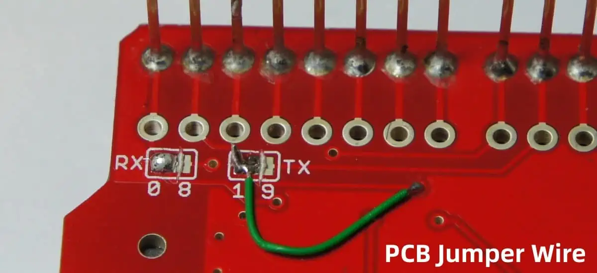
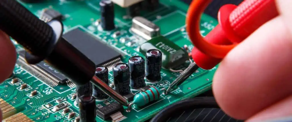
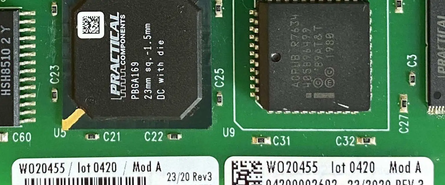
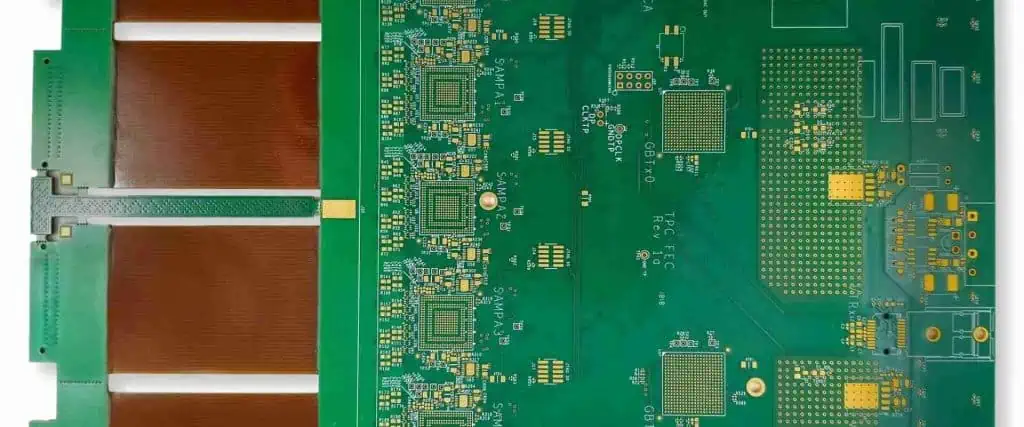
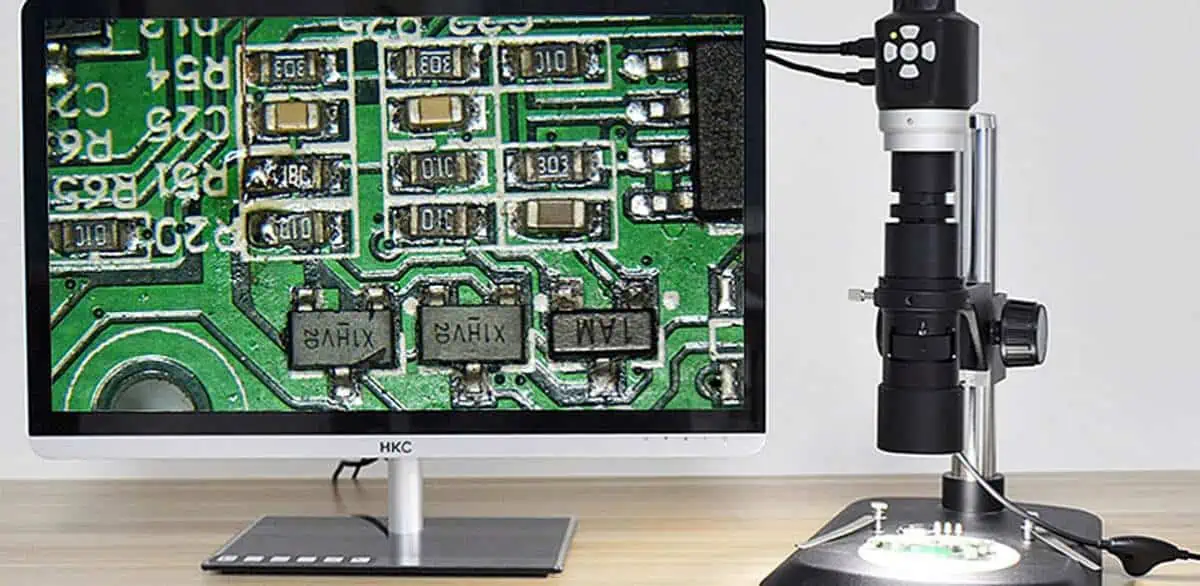
Printed circuit board (PCB) manufacturing involves stringent quality checks to validate fabrication accuracy before shipment. Visual inspection remains indispensable for verifying PCB layer alignment, pad geometries, soldermask tolerances, and confirming drill hole sizes across boards utilizing specialized inspection microscopes providing high quality imaging.

However, with ongoing PCB technology advancements enabling smaller line widths, tighter pitches and finer tolerances, traditional stereo optical microscopes prove inadequate necessitating more advanced magnification solutions.

This article outlines key considerations when selecting PCB inspection microscopes, examines popular models, and provides a feature comparison across different price categories to help identify the best value options.

YouTube video

Importance of Visual PCB Inspection

Automated optical inspection (AOI) systems employing sophisticated imaging techniques provide first-line quantitative dimensional analysis checking PCB panels for defects during fabrication. However, final quality assurance requires detailed physical verification against pertinent design specs.

Engineers perform various critical validations only possible through visual examinations under microscopes, including:

Trace Width Measurements โ€“ Confirming etched conductor widths match layout rules across different PCB routing layers

Pad Spacing Analysis โ€“ Verifying clearance tolerances between closely spaced pads or vias

Soldermask Inspection โ€“ Checking for complete paste coverage with no voids or scratches

Conductor Roughness โ€“ Detecting pits, nicks or inconsistent metal etch roughness along traces

Plating Integrity โ€“ Validating uniform copper, tin, silver or gold plating thickness on pads

Drilling Circularity โ€“ Assessing drill hole diameter consistency and edge roughness

Step-and-Repeat Accuracy โ€“ Measuring alignment marks validating pattern overlay precision

wegewVoiding โ€“ Detecting insufficient filler or air gaps around pads on soldermask or metal layers

Since these dimensional verifications require micron-level imaging resolutions, PCB designers need access to advanced magnification systems during final board bring-ups while avoiding cost overkill.

Types of PCB Inspection Microscopes

Several optical instrumentation solutions assist PCB analyses:

Stereo Microscopes

Stereo microscopes contain paired eye tubes with separate light paths providing slightly offset images recombined by the visual cortex into enhanced 3D depth perception without fish-eye distortion at lower 5-100x magnification ranges. Large working distances accommodate inspecting populated PCB assemblies. However, resolution proves inadequate assessing finer fab layers.

Compound Microscopes

Compound microscopes employ a two stage magnification system with initial 10-100x magnification from an objective lens followed by added 10-15x eyepiece zoom boosting overall viewing up to 1500x levels necessary for detail PCB analyses. High numerical aperture objectives enhance resolution but limit working distances. Mounted camera modules assist image capture across smaller fields of view during PCB examinations.

Digital Microscopes

These eliminate conventional eyepieces replacing optical tubes with high resolution CMOS/CCD imaging sensors providing magnification levels up to 300x when coupled to large HD displays. However, lower sensor pixel density restricts resolving capacity crucial for PCB work. Touchscreen manipulation conveniences standalone operation but subjects displays to contamination.

Measuring Microscopes

Measuring microscopes incorporate high precision linear encoded or rotary stages coupled to fine-adjustment focusing nosepieces providing micron-level X-Y positioning repeatability essential for dimensional metrology. Glass reticle overlays or software-based gridlines enable measuring key PCB features like conductor spacing, hole sizes or land widths. However bulk hampers manipulation flexibility.

Benchtop Microscopes

Benchtop models with boom stands keep main optical assembly base stationary while allowing adjustable slide stages or camera tubes to move facilitating inspection access across large PCBs with flexible side-on viewing. Extended working distances accommodate examining populated boards or instances needing auxiliary lenses attachment. High intensity ring lights assist surface illumination.

Key Specifications for PCB Inspection

Microscope selection factors include:

Magnification Range โ€“ 100x-500x levels necessary for tracing conductors or examining drill hole walls by resolving sub-25-micron features

Working Distance โ€“ At least 6 inches provides clearance inspecting dense bottom-side components on multilayer PCBs

Illumination โ€“ Ring lights with diffused LEDs prevent harsh reflections across copper layers

** resolving** โ€“ Diffraction-limited optics reduce aberration enhancing edge visibility

Field of View โ€“ Larger viewing facilitates quicker area scans during PCB analyses

Zoom Ratio โ€“ 10:1 or higher provides sufficient magnification latitude

Camera Sensor โ€“ High density CMOS/CCD sensor assist capturing intricate PCB details

Optomechanical Stage โ€“ Motorized precision XY stage allows programmable board navigation

Software โ€“ Measurement software checks component locations or sizes

Ergonomics โ€“ Articulating arms or boom stands improve user adjustability

By optimizing these parameters, inspection microscopes facilitate detailed PCB assessments necessary before approving boards for production deployment.

Comparison of Popular PCB Inspection Microscope Models

ModelKey FeaturesPrice
AmScope SE400-Z Professional Binocular Stereo Microscope– Magnification up to 120x- 10x Eyepieces + 4x Objectives – LED illumination – 7″ x 5″ Stage$170
Celestron 44341 Advanced Stereo Microscope– Magnification up to 40x- 10x Eyepieces + 4x Objectives – Diascopic illumination – Built-in 0.5MP Camera$230
AmScope SM-3TZ Professional Trinocular Stereo Zoom Microscope– Zoom Magnification 0.7x – 4.5x – LED illumination – Camera output – 7″ x 7″ stage$950
AmScope SE306R-PZ Forward Binocular Stereo Microscope– Magnification up to 70x – 20x Eyepieces + 3.5x Objective – Dual LED lights – Articulating boom arm stand$600
BW Optics Signature Series Compound Microscope– Magnification up to 2000x – Siedentopf binocular head – Koehler illumination – 10x Eyepieces + range of objectives$2,000
AmScope SM-1TSZ-L6W-10M Digital Professional Microscope– Magnification range 20x – 230x – CMOS sensor up to 5MP – WiFi connectivity – Software measurement – LED illumination$700
Vision Engineering Lynx EVO Benchtop Measuring Microscope– Magnification up to 215x – Motorized 200x175mm stage – 36x44mm field of view – Software based measurements$20,000
Leica DMS1000 Digital Measuring Microscope– Magnification up to 300x – Motorized 175x175mm stage – 36x44mm field of view – 0.9 ฮผm resolution – Leica software suite$30,000

This comparison summarizes capabilities across various price points highlighting factors that deeply impact resolution critical for PCB validation. Mid-range models offer best value balancing performance and affordability.

Software Features for PCB Inspection Microscopes

Integrated software and analysis packages enhance productivity when evaluating boards:

Digital Image/Video Capture โ€“ High resolution camera sensor enables recording intricate PCB details far exceeding visual observations or basic smartphone images

Measurements Overlay โ€“ Onscreen gridlines or overlays precisely quantify X-Y distances, diameters, areas etc

Stepper Motor Driven Stage โ€“ Software-controlled motorization allows fast navigation across large boards

Image Stitching โ€“ Seamlessly stitches multiple captured frames into one composite image covering bigger board sections

Cloud Connectivity โ€“ Connects globally distributed engineering teams by sharing findings real-time over cloud servers

Custom Reporting โ€“ Automatically generates detailed PDF reports compiling measurements, annotations and visual evidence documenting PCB analyses

Such features improve inspection workflow efficiency and traceability across teams when validating during PCB fabrication events or post-assembly.

Inspection Methodology for PCB Validation

Follow these best practices when examining boards:

Whole Panel Scans โ€“ First visually inspect the entire panel utilizing lower magnification to catch potential scratches, discoloration or debris across boards

Layer Progressions โ€“ Gradually increase magnification in a methodical manner starting from outer layers before examining inner layers to map entire PCB stackups

Frequent Cleansing โ€“ Use lint-free swabs dampened with reagent grade isopropyl alcohol often when cleaning optics or boards during inspections to avoid contaminants obstructing visuals

Light Adjustments โ€“ Tune brightness levels and diffusers to clearly illuminate focus areas without blowing out sheens or producing reflection artifacts

Cross-Polarization โ€“ Adding cross polarization attachments aids enhancing contrast revealing otherwise barely visible micro-cracks or fractures in conductors

Dimensional Sampling โ€“ Take measurements across evenly sampled areas capturing edge use cases rather than focusing solely only one location

Image Captures โ€“ Extensively photograph abnormal dimensions deviating from baselines providing tangible proof of defects

Electrical Validation โ€“ Confirm minimum aperture openings satisfy target impedance levels through electrical impedance testing

Implementing careful inspection processes strengthens defect detection accuracy necessary to meet stringent quality thresholds expected of PCB solutions before deploying boards across applications.

Maintaining PCB Inspection Microscopes

Routine care optimizes microscope functionality:

  • Daily Cleaning โ€“ Gently blow away loose dust using a blower before wiping down components using acceptable solvents; keep optics capped when not in use
  • Storage Precautions โ€“ Engage slide locks, lower stage platforms, retract cord/cables, and cover equipment to prevent mechanical damage
  • Mishandling Avoidance โ€“ Transport microscopy systems safely avoiding bumps/vibrations and store in acceptable temperature/humidity levels
  • Lubrication Scheduling โ€“ Apply small drops of rotating stage lubricants biannually ensuring smooth friction-free adjustments
  • Lens Checks โ€“ Periodically inspect objective lens surfaces for oil/dirt buildup degrading clarity or scratches impairing resolution
  • Validation Calibration โ€“ Conduct annual calibration verification against validation standards traced to international metrological institutes to confirm measurement equipment retains precision

While proper maintenance activities ensure optimal microscope health maximizing equipment lifetime at minimum costs, lack of appropriate care risks performance deterioration or early failure losing value of analytical investments.

Future PCB Inspection Technology Trends

Emerging solutions improve microscope-based printed circuit analyses:

Automated Platforms โ€“ Motorized programmable XY stages with cameras, precision movements and onboard analyses minimize user intervention while tirelessly executing inspection test suites at machine vision levels unattainable manually

Hyperspectral Imaging โ€“ Advanced sensors providing enhanced spectral contrast discern minute material variances better differentiating conductor edges or minuscule defects

Artificial Intelligence โ€“ Trainable computer vision techniques reliably classify defect types automatically without operator expertise speeding analytics

Holographic Imaging โ€“ Laser-based holographic interference magnification achieves nanometer-scale 3D optical resolution better resolving microstructural intricacies within glass fibers or laminate weaves

Big Data Trending โ€“ Extensive archival image datasets pooled across PCB batches subjected to advanced analytics algorithms determine control thresholds differentiating acceptable process variations from true defects highlighting only statistically significant outlier conditions requiring corrective actions

Such emerging technologies will significantly advance reliability, repeatability and accuracy of future PCB inspection systems well beyond conveniences provided by basic optics thereby further enhancing fabrication quality.

Conclusion

This guide examined why achieving optimal magnification, contrast, working distances and resolution prove essential for verifying key electrical, dimensional and structural parameters during printed circuit analyses using microscopes. Mid-range models balance affordability without sacrificing longevity or analytical flexibility expected for PCB design applications, whereas premium microscopes deliver ultimate precision necessary for leading-edge solutions. Adopting robust inspection methodologies coupled with proper instrument care maximizes measurable returns when evaluating bare PCB boards primed for electronics integration. Going forward, continued innovations across AI-enabled automation, sensor technologies and imaging modalities will reshape quality assurance processes.

Frequently Asked Questions

What kind of microscope is needed to inspect PCBs?

Validating modern complex PCBs requires stereo microscopes offering at least 70x magnification with 8x eyepieces plus 5x zoom capacity and extended 10+ inch working distances for inspecting populated boards. Adjustable ring lights prevent reflections across bare copper layers. Boom arm stands aid ergonomics while probes inspectors access hard-to-reach solder joints or vias across boards.

Why are measuring microscopes used to examine PCBs?

Measuring microscopes incorporate precision movement stages, reticle overlays and metrology software needed for quantifying key PCB conductor widths/spacings, annular rings, drilling registration marks or step-and-repeat spacing essential for verifying dimensional accuracy and overlay alignment critical before deploying boards lacking normal length-scale visual cues available for assessing macro-sized objects.

What are must-have features PCB inspection microscopes?

Quadruple air objective revolvers ensure highest magnification range up to 500x examining ultra-fine traces below 100 microns coupled with adjustable focus to accommodate onboard components. Wide 22mm fields of view quicken inspection together with flexibility to add auxiliary lenses. Long working distances facilitate examining hidden solder joints. XY motorized stages enable automatic beneath-board navigation. High color rendition ring lamps prevent metallic sheen blowouts.

Why is ESD protection needed when inspecting PCBs?

Since even intermittent ESD discharges risk irreparable damage destroying susceptible onboard electronics during power-up initialization, technicians must follow stringent anti-static protocols including wearing grounded wrist straps; avoiding nylon clothing during analysis; operating microscopes only at grounded workstations equipped with ESD flooring, point ionizers and humidity controllers; while preventing static charge buildup across objective lenses or PCB handling carts through topical sprays helping safeguard inspected boards.

What level of optical magnification is necessary for inspecting 01005 passives?

With ultra-miniature 01005 SMD components measuring just 0.4mm length/width above boards, validating solder fillet profiles, pad alignments or marking legibility requires minimum 250x magnification with the optical resolution to discern micron-scale features only feasible using high power objectives available with premium compound microscopes configured for such extreme CMOS silicon wafer metrology thereby allowing engineers characterize fabrication efficacy necessary for handling next-generation 01005 density assembly demands.

What Is a Jumper Wire PCB?

A jumper wire is a conductive connector used to join two points in an electronic circuit on a printed circuit board (PCB). Jumper wires act as a shortcut to avoid having to route printed metal traces on the PCB to make connections between distant pads or traces. They are also used to temporarily bypass components or reroute signals during circuit prototyping or testing.

On PCBs, jumper wires allow signals in a circuit to be conveniently bridged without the layout effort of etching multiple PCB layers when routing dense designs. This article provides a detailed overview of various types of jumper wires used in PCBs and their applications.

Types of Jumper Wires

Jumper wires come in several configurations best suited for particular use cases:

Solid Copper Jumpers

A solid copper wire forms the simplest jumper connection between PCB points. Simple copper wire cut to size and soldered to pad connections serves adequately to bridge short jumper links up to an inch or less. Round or square cross-section solid copper magnet wire is commonly used. The thickness ranges from 18 AWG to 26 AWG.

Solid copper wire PCB jumpers

Stranded Jumpers

Stranded jumpers use multiple thin copper wire strands twisted or braided together to form a thicker cable jumper. Stranded wires provide flexibility easing routing through cramped layouts and installation across solder terminals. Common configurations employ stranded 22 AWG โ€“ 30 AWG jumper sets. Flux-core solder wicking assistsstranded jumpersโ€™ solderability.

YouTube video

Braided flexible stranded copper wire jumper

Insulated Wire Jumpers

Insulated solid core or stranded copper wire jumpers jacketed with plastic, rubber or lacquer coatings prevent accidental short circuits to nearby pads or board features during jumper installation in complex, density PCB designs. The insulation electrically isolates the conductive core. Heat shrink tubing also protects jumper segments. Insulation colors help visually trace custom jumpers across boards.

PVC-insulated solid copper jumper wire above PCB

Preformed Jumpers

Pre-shaped jumper wires are molded into particular shapes using plastic or nylon sleeves between the endpoints allowing installation directly above components or around obstacles on crowded PCB boards without interference. By providing precisely defined stand-off heights and custom shapes conforming to circuit layouts, preformed jumpers offer reliability combined with adaptability across circuit boards.

Preformed jumper with stand-offs clearing nearby capacitors during installation

Ribbon Cable Jumpers

Using ribbon cable as jumpers on PCBs provides multiple signal connections in parallel. The flat flexible ribbon style jumper can integrate bulk wire tracking between connectors and cable assemblies laid conveniently across PCB sections with easy individual wire access. Ribbon jumper assemblies may interface external low-voltage differential signaling (LVDS) displays, keypads or cable harnesses across boards.

Rigid-Flex PCB Jumpers

Rigid-flex PCBs utilize flexible PCB extensions with embedded thin copper traces to structurally interface separate rigid PCB assemblies eliminating wired jumpers. The integrated flex jumpers folded tightly or contoured enable 3D compaction joining multilayer boards internally across devices eliminating external cabling while conducting signals reliably through flat flex bends without distortions.

PCB Jumper Wire Applications

Jumper wires satisfy diverse connectivity requirements across various kinds of PCBs:

Prototyping

Breadboards extensively use jumper wires allowing designers to conveniently bridge components and ICs laid out temporarily to validate circuit concepts without finalized PCBs. Solid core and stranded jumpers of easily customized lengths facilitate routine reconfigurations as designs evolve through iterative testing before PCB fabrication. Prefabricated jumper sets simplify prototyping.

Circuit Modifications

On existing PCBs, jumper wires bypass components or reroute signals during circuit modifications or corrections. Removed links are bridged or alternate board connections established for validating upgrades. Insulated jumpers prevent short circuit mishaps across increasingly congested boards. Stranded jumpers handle frequent alterations as circuits morph across multiple PCB revisions.

Density Constraints

Interconnecting distant terminals across complex high density PCBs like GPS receivers avoids extensive routing across multilayers when jumpers shortcut pads spaced far apart. Direct fly-over jumper links simplify layouts in dense designs. Right-angle jumpers clear components when bridging tight spaces. Stand-off spacers provide proper clearances.

Shield Jumpers

Solutions requiring careful impedance control at high frequencies utilize coaxial or twisted pair cables as shielded jumpers to contain electromagnetic interference (EMI). Miniature surface mount (SMT) coaxial connectors solder with adjacent ground vias suppress noise injection in multi-layer boards. Ferrite beads aid isolation.

Programming Headers

Specialized application boards may employ dual-row male pin headers as programming interfaces allowing temporary interfacing with external electronic modules or cables to update firmware or modify settings through serial data connections bridged using female-to-female jumper wires. Right-angle pin headers conserve space.

Test Points

Onboards lacking test points utilize jumper wires to sample internal signals by splicing connections onto nodes otherwise inaccessible without drilling holes on multilayer boards. Rigid tips of test probe jumpers securely latch onto solder pads, vias or component leads to non-invasively monitor waveforms for debugging firmware or diagnosing faults.

Best Practices When Using PCB Jumpers

Follow these guidelines to employ jumpers effectively while avoiding common mishaps:

  • Use stranded wires offering flexibility for alterations
  • Keep conductors short limiting parasitic inductance
  • Define schematics/layouts clearly highlighting jumpers
  • Insulate wires preventing accidental shorts
  • Install spacers when bridging tall components
  • Shield noisy or susceptible high-frequency paths
  • Secure wires against vibration failures
  • Logically label custom jumpers connections
  • Limit current levels for thinner gauge wires

Advantages of Jumper Wires for PCBs

Jumper wires offer multiple benefits for connecting points on printed circuit boards:

Simplicity

Jumper wires facilitate rapid connections between existing PCB pads bypassing complex multilayer routing. Prefabricated jumper sets quicken prototyping iterations.

Adaptability

Flexible jumpers allow adjustments as design requirements evolve across future board spins. Stranded wires make alterations easier by avoiding cracked joints or damaging rigid traces.

Space Savings

Direct fly-over jumpers conserve routing real estate in cramped layouts by circumventing the need to accommodate tracing channels on all layers during multilayer PCB fabrication.

Reliability

Short jumper wire links avoid issues like opens or electrical noise compared to tiny width PCB traces spanning larger distances across boards prone to damage. Minimal solder joints also enhance dependability.

Reconfigurability

Jumpers permit customizable connectivity only finalized post-fabrication allowing designers experimenting with schemes unforeseen during CAD PCB layout stages as additional functionality gets incorporated across boards.

Economy

Supplemental jumpers mitigate complete PCB respins whenever minor circuit changes emerge saving time and costs. Jumpers also simplify specialized connectivity demands tailored per end-application without elaborate custom routing.

Design Simplicity

Using jumper wires keeps multilayer PCB stackups simpler by reducing layer count needs with fewer traces since jumpers bridge connections directly sans dedicated routing. This avoids intricate impedance tuning.

Disadvantages of Jumper Wires for PCBs

However, PCB jumper wires also come with some downsides:

Clutter

Excess jumpers crisscrossing a PCB board appears messy complicating visual inspection and physical access during rework or manual assembly especially on double-sided boards. Insulation sleeving colors help identify custom jumpers.

EMI Susceptibility

Lengthy unshielded jumper wires act as antennas injecting unwanted external electromagnet noise into sensitive circuits lacking proper guarding traces or ground isolation. This risks signal integrity issues on boards lacking proper stackup shielding.

Reliability Concerns

Mechanical stress across soldered joints or copper wire fatigue due to perpetual vibration in industrial environments risks intermittent failures over prolonged deployment durations compared to integrated PCB traces or flex circuits. Periodic inspection for cold joints or broken leads is necessary.

Switching Noise

High frequency jumper links exceeding mere inches undergo impedance mismatches potentially injecting reflections. Excessive length risks ground bounce or crossover ringing across jumper wire stubs degrading signal quality in multi-GHz circuits. Terminations may become necessary.

Assembly Issues

Hand soldering jumper wires proves trickier as PCB complexity increases due to tight clearances raising chances of short circuits or bridging solder between closely spaced surface mount device (SMD) pads when integrating supplemental jumpers across populated boards using manual rework stations.

Comparison Between PCB Traces Vs. Jumper Wires

ParameterPCB TracesJumper Wires
Path LengthsUnlimited routingShort distance links
FlexibilityFixed routingAdjustable terminations
ImpedancesPrecisely controlledHard to characterize
Switching SpeedsMulti-Gbps supportLimited to lower frequencies
Integration ScopeEntire PCB conductive networkLocalized bridges
Directional ChangesAny angleLimited without conductors kinking
InductanceLowerIncreased due to wire loops
Parasitic CapacitanceHigher at PCB dielectric-copper interfaceLower in air medium
Noise SusceptibilityGuard rings and ground planes aid shieldingMore prone to external interference
Current CapacityHigh for thick copper layersThinner wires impose limits
Design FinalityFixed layout after fabricationAdjustable during use
Cost FactorsHigh initial PCB fabrication expensesLow supplementary jumper wire costs

In summary, while jumper wires adequately serve simpler connectivity needs, accommodating high-complexity multi-Gbps transfers across large boards requires precision routing to exacting impedance specifications only feasible through integral PCB metallization layers. Supplementary jumpers handle secondary localized connections.

Future PCB Jumper Wire Trends

Wireless Charging
Wireless Charging

Emerging jumper wire technologies help address existing capabilities regarding flexibility, speed and integration:

Active Optical Cables

Optical fibers replace copper jumpers for achieving high-bitrate low-loss links across backplanes. Miniaturized vertical-cavity surface-emitting lasers (VCSEL) and photodiodes integrated using chip-scale packaging techniques enable board-level optical interconnect bridges.

Carbon Nanotube (CNT) Conductors

CNT wires with high conductivity and current capacity improve jumper links for power delivery. Low inductance assists RF performance. The inherent durability surpasses copper becoming vital in aerospace systems.

Graphene Jumpers

Graphene films screen-printed onto flexible substrates that planarize onto surfaces will replace rigid jumpers. The excellent conductivity minimizes losses across folded graphene junctions. Easily customizabled graphene jumpers printed directly onto rigid or conformal surfaces become feasible.

Active ICs

Integrating tiny ICs like signal buffer/retimers using chiplets directly onto jumper wire assemblies boosts signal integrity when bridging longer traces or off-board cabling in high-speed serial links. Termination resistor chiplets also assist impedance matching.

Programmable Jumpers

Electronically switchable conductors utilizing micro-electromechanical (MEMS) actuators modify jumper connectivity. This allows changing board interconnect schemes dynamically through software reconfigurations as system requirements change eliminating manual jumper wire adjustments.

Conclusion

Jumper wires continue serving diverse connectivity demands across prototype and production PCBs thanks to simplicity and customizability despite limitations in supported distances, operating frequencies and integration challenges. Judicious utilization balancing impedance control, noise and assembly factors helps maximize utility. Moving forward, emerging jumper technologies will address existing constraints related to performance, reconfigurability and integration.

Frequently Asked Questions

How are jumper wire lengths calculated?

Jumper lengths equal the linear distance between connecting terminals plus any vertical rise above tallest components or PCB features along the bridged path. Right-angle connections require defining both horizontal and height spans to reach elevated board targets allowing safe jumper installation preventing short circuits. Extra tolerance additionally cushions links stretching during usage.

What gauge jumper wire connects GPIO pins?

General-purpose input/output (GPIO) pin interfacing requires minimum 22 AWG jumper wires to safely carry related currents while keeping inductance lower for better high frequency response during GPIO voltage transitions necessary to prevent signal integrity issues. Thinner 26-30 AWG works for low power GPIO banks. Stranded wires enhance flexibility.

How to connect ribbon cable jumper to header pins?

Ribbon cable jumper connections onto header pin rows is best accomplished by carefully aligning the ends across both rows before tightly crimping down insulation displacement connectors. This pierces the insulation allowing the flattened ribbon wire strands to make contact with the underlying male header pins eliminating tedious hand soldering. Strain relief backings prevent cable flex damage.

Why are coaxial cables used for shielded jumpers?

The coaxial construction offers excellent noise immunity by providing constant impedance low inductance signal conductor paths where the central signal core wire gets thoroughly shielded against external electromagnetic interference along the entire shielded jumper wire length using the outer grounded braided metal mesh or metallic foil layer separation by a dielectric insulator. This prevents crosstalk issues.

What safety precautions should be taken when using jumper wires?

It is critical to prevent short circuits during jumper installation across crowded PCB assemblies through steps like using insulated wires, installing wire spacers, securing wires against accidental movement, safely routing wires avoiding nearby board features, ensuring adequate insulation thickness for voltage isolation, proper wire current ratings, checking for exposed conductors potentially contacting pads, verifying broken leads etc. This avoids catastrophic failures.

Stripboard Vs Perfboard Vs Breadboard: What’s Difference

When building electronic circuits, enthusiasts and engineers often need to prototype on something before committing to a custom printed circuit board (PCB) design. The three most common prototyping boards are stripboard, perfboard, and breadboard. But what exactly is the difference between them and when should you use each one? This guide will explain the key differences and help you choose the right option for your project.

Overview Comparison

Here is a high-level overview comparing stripboard, perfboard, and breadboard:

Board TypeDescriptionKey BenefitsBest Uses
StripboardFibreglass board with copper strips running across one sideInexpensive, easy to solder complex circuitsSemi-permanent circuits and prototypes
PerfboardFibreglass board with a matrix of holes plated with copperFlexible layouts, easy to solder componentsLow-volume production of simple circuits
BreadboardPlastic board with metal spring clips under the holesNo soldering required, easy prototypingTemporary circuits, testing components/layouts

Now let’s explore each of these prototyping boards in more detail.

Stripboard

Stripboard (also known as Veroboard) consists of a thin, insulating fibreglass board with copper strips running across one side. The strips are spaced at standard 0.1″ pitch, and there are usually 24 or more strips across a typical board.

Stripboard gets its name from the copper strips that run across the board. These provide an easy way to make electrical connections without any soldering. Components can simply be pushed into the board to straddle a copper strip. The strips connect rows of holes together in one direction.

Some key benefits of stripboard include:

  • Inexpensive – Stripboard is an affordable prototyping option. Boards are available in various sizes for just a few dollars.
  • Easy to solder complex circuits – The copper strips provide a convenient distribution bus to wire up circuits by soldering components between strips. Through-hole components can be securely mechanically anchored to the board.
  • Semi-permanent – Circuits assembled on stripboard are more permanent than breadboards since components are soldered in place. But the board itself can be reused.

Stripboard is a good choice when you want to create a semi-permanent prototype of a complex circuit cheaply without designing a custom PCB. It may also be suitable for short production runs once the design is finalized. Stripboard allows relatively easy changes too if modifications are needed subsequently.

PCB Transfers

An advantage of stripboard is the ability to transfer the layout to a custom PCB fairly easily. Once the circuit is working on stripboard, the layout can be replicated by drawing the PCB layout to match the placement of strips and breaks. Most PCB design software has stripboard layouts templates built-in to assist the transfer.

Perfboard

Perfboard, as the name suggests, contains a matrix of small holes plated with copper – similar to the perforations used to facilitate board separation on a finished PCB. This allows wires and component leads to be poked through and soldered to construct a circuit.

Unlike stripboard, there are no copper tracks connecting the holes on perfboard. Instead, you must manually make all the connections with wire between components. This allows fully custom layouts.

Some key characteristics and benefits of perfboard:

  • Flexible layout – With no predefined tracks, you can place components anywhere in your own desired layout. Routing wires point-to-point is easy.
  • Low-volume production – Perfboard allows reasonably straightforward assembly of simple verified circuit designs for small production runs.
  • Easy soldering – Through-hole components and wires can be securely soldered to the copper pads around each hole.

Perfboard is a better choice than stripboard for small scale manufacture of simple boards once prototyped, as placement is more flexible. It may also suit experimental circuits where connections need to evolve incrementally.

Pros vs Cons vs Stripboard

Comparing perfboard and stripboard:

  • Perfboard layouts are more flexible than stripboard
  • Stripboard makes basic linear circuits quicker to assemble without wiring
  • Perfboard requires all connectivity to be manually wired
  • Perfboard does not provide mechanical anchorage for surface mount components

So in summary, perfboard supports more customization but stripboard is simpler for basic linear track layouts.

Breadboard

Breadboard (also known as plugboard) is used for creating temporary prototypes. It contains a perforated plastic board, with an array of metal spring clips under the holes. Components are plugged into the holes, and the clips make electrical connections without any soldering.

The spring clips are arranged underneath in rows, connected horizontally, with splits between rows running vertically across the board. This breaks the rows into short 5-hole strips. Typically there is also a vertical ditch bisecting the board into left and right sections.

Key attributes of breadboards:

  • No soldering – Components push directly into the holes for instant connections and prototyping
  • Temporary circuits – It’s quick to plug components in, but they also pull out easily later for reconfiguration
  • Test layouts and experiment – Easily add, remove or shuffle parts to rapidly test circuit ideas

Given the temporary nature, breadboard is most suited to initial experimentation with circuit ideas, verifying component combinations, testing modules in different layouts, and similar tasks for quick prototyping.

Complex or high frequency designs may suffer performance issues on breadboard due to resistance/capacitance of the contacts. The loose mechanical anchorage can also cause problems. So verified layouts tend to migrate to more secure stripboard or perfboard for robustness.

Mini Protoboards

For installing small breadboard prototypes into semi-permanent products rather than strip/perf, mini protoboards are available. These have standard breadboard hole spacing but secure mechanical mounting and solderable pads/traces on the underside.

Additional Comparison Points

Beyond the core characteristics already covered, here are some other considerations when selecting between stripboard, perfboard and breadboard:

Ease of Use

  • Breadboard is the quickest to prototype on initially
  • Stripboard allows faster assembly than perfboard for linear tracks
  • Perfboard most time consuming to assemble from scratch

Connectivity

  • Breadboard has split sections with vertical disconnects midway
  • Stripboard provides horizontal connectivity along continuous tracks
  • Perfboard requires manual wiring of all connectivity

Mechanical Stability

  • Breadboard provides the least secure component anchorage
  • Stripboard components anchored by solder connections
  • Perfboard anchors via solder but may use adhesive too

Reconfigurability

  • Breadboard is designed for convenient rework and layout changes
  • Stripboard allows some layout tweaks but best for semi-permanent
  • Perfboard can be changed but reworking is more difficult

Appearance

  • Breadboard typically has colored clips, symbols, markings to assist
  • Stripboard and perfboard just have a grid of holes with no annotations

Hopefully this gives you a better understanding of how to differentiate stripboard, perfboard and breadboard prototypes boards. To summarize:

  • Use breadboards for initial temporary prototyping
  • Stripboard suits semi-permanent medium complexity boards
  • Perfboard fits simpler custom layouts or low-volume production

There are also various other specialized prototyping boards, but these are the most ubiquitous.

Frequently Asked Questions

What are the key differences between stripboard and perfboard?

The main differences are:

  • Stripboard has predefined copper tracks connecting rows of holes
  • Perfboard has an array of holes but requires manual connectivity
  • Stripboard allows easier prototyping of linear circuits
  • Perfboard supports fully custom component placement

Is stripboard the same as Veroboard?

Yes – stripboard and Veroboard are different names for the same type of prototyping board.

Can I use perfboard to make multiple copies of a working circuit?

Yes, perfboard allows reasonably straightforward small-scale production once a reliable circuit design is finalized. The assembled boards can replicate stripboard prototypes, for example.

When should I transition from breadboard to stripboard?

It’s best to transfer a circuit from breadboard once the design is functionally proven and you need a more rugged, permanent prototype for further testing or practical usage.

What are breadboard jumper wires and why are they used?

Breadboard jumper wires have rigid tips on the ends that fit securely into the board holes. They allow solid connectivity between non-adjacent rows on the breadboard which have breaks between the spring clips underneath.

How to Build PCB Kits

A PCB kit refers to an electronic project with a pre-made printed circuit board and collection of necessary components provided to the end user for assembly and testing. PCB kits offer an accessible starting point for electronics hobbyists and STEM students to gain hands-on learning without complex fabrication or sourcing tasks.

This guide covers key steps in the PCB kit build process including:

  • Understanding kit documentation
  • Identifying and organizing components
  • Preparing for assembly
  • Soldering techniques
  • Final assembly and troubleshooting

Weโ€™ll explore best practices to smoothly take your kit from box to finished circuit board. Letโ€™s get started!

Kit Documentation

PCB kits include documentation detailing the board layout, schematic, bill of materials (BOM), assembly instructions, and often functional descriptions and operating theory. Thoroughly reviewing this content before starting provides the necessary context for the build.

Typical documentation items:

  • Board visual – component placement reference
  • Schematic – circuit diagram
  • BOM – list of all included components
  • Build guide – step-by-step assembly instructions
  • Theory overview – high level functional description

Ensure you read over all materials and understand at a high level how the circuit works along with specific build requirements before picking up the soldering iron!

Sorting and Identifying Components

The BOM lists every resistor, capacitor, IC, connector and other elements included in your PCB kit. Double check all items against the list:

  • Verify quantity of each component value
  • Some kits organize parts in separate marked bags
  • Larger components may be individually packaged

Next, arrange parts categorically to simplify locating specific items during assembly. Sort them into intuitive groupings:

Example grouped layout:

  • Resistors
  • Capacitors
  • Diodes
  • ICs
  • Transistors
  • Connectors
  • Hardware etc.

Consider using small containers to minimize risk of loss. This organization drastically speeds up component retrieval compared to digging through a pile of random parts!

Tools and Preparation

Before soldering ensure you have the necessary equipment setup:

Recommended items:

  • Soldering iron + stand
  • Thin gauge leaded solder
  • Flux pen + solder braid
  • Flush cutters + tweezers
  • Magnifying glass
  • Multimeter
  • Safety glasses

Also get any required peripherals like power adapters or programming cables to ultimately operate the board.

Clear sufficient workspace and eliminate clutter. Having an orderly soldering area prevents losing tiny components amidst piles of wires and tools!

Soldering Technique

Weโ€™ll quickly cover some key pointers before firing up the iron:

  • Carefully identify pad 1 and orientation markers
  • Double check component values before insertion
  • Load solder on one pad, heat and push component in
  • Reheat to flow solder to other pad
  • Inspect for shorts, leftover flux etc.
  • Seek 2nd opinion for complex assemblies

Additionally here are useful practices:

  • Position board vertically to avoid slipped parts
  • Start with physically larger components
  • Work methodically following assembly guide
  • Take breaks to rest your eyes

Patience and care pays dividends versus rushing assembly and causing avoidable mistakes or component damage.

Mounting Sensitive Components

Certain components require special handling:

ICs and Sockets

When soldering ICs directly to boards take care with heat levels. Use sockets if available to minimize thermal stress. Align notches and double check orientation.

Electrolytic Capacitors

Mind polarity! The longer lead and case stripe denotes positive. Mount vertically wherever possible.

Diodes

Align line on component body to printed orientation on PCB symbol.

Connectors

Ensure they site flush to the board prior to soldering all pins.

There are many other tips and tricks – consider SparkFunโ€™s excellent guide covering proper technique.

Final Assembly

Once all components are soldered, perform the following checks before applying power:

? Visual inspection – Confirm proper seating, orientation and neatly trimmed leads

? Continuity check – Verify electrical connections between pads with no shorts

? Compare with reference image(s) – Validate correct realization of board assembly

Assuming all looks good, connect programming cable or load batteries/power adapter, cross your fingers and flip the switch!

Troubleshooting

If your board doesnโ€™t spring to life, some steps to isolate potential issues:

? Power validation – Double check voltage at expected terminals

?๏ธ Thermal checks – Feel for hot components signaling shorts

? Resistance measurements – Take readings pin-to-pin verifying expected values

? Comparative analysis – Diff schematic vs assembled board connections

? External factors – Try known working substitutes for peripherals

Methodically testing validated working sub-circuits can help identify faults down to the component level through a process of elimination.

Donโ€™t be discouraged by build issues โ€“ solving them leads to greatly deepened knowledge, often beyond what smooth assembly alone provides!

Conclusion

Building PCB kits develops well-rounded electronics expertise spanning theory, assembly, debugging, and harmless failure recovery. These skills translate directly into testing and modifying commercial products or developing entirely new circuits.

With so many high quality kits available on fascinating topics from retro gaming to robotics vision and beyond, the educational possibilities are boundless. Constructing even basic blinky boards imparts device comprehension far beyond just buying something off the shelf.

Now that youโ€™re equipped with a thorough foundation in DIY kit creation, itโ€™s time to bring your electronic visions to life!

Frequently Asked Questions

Q: Do I need to be an electrical engineer or expert to build a PCB kit?

A: Not at all! Many kits come with extensive documentation walking you through all necessary steps with no assumptions of prior knowledge. Focus is more on following instructions, soldering and construction skills over pure circuit theory comprehension.

Q: Can damaged parts be replaced if I make a mistake?

A: Most kit sellers offer reasonably priced replacement components available on their website. Some even provide โ€œCrash Kitsโ€ with extra ICs, connectors etc. anticipating common mishaps from the less experienced.

Q: What tools should I invest in if pursuing electronics kits as a hobby?

A: Start with a basic ~40W soldering iron, thin rosin core solder, flush cutters, needle nose pliers, a multimeter and magnifying glass. Down the road, handy additional tools would include solder sucker/solder wick, digital microscope, helping hands jigs, a larger 70W iron and more.

Q: Is it safe to allow kids to build kits with supervision?

A: Using child-friendly soldering iron variants with reduced operating temperatures, most children 10+ with close parental oversight can successfully assemble basic kits. Ensure to emphasize safety like wear eye protection, tie hair back, avoid touching the hot tip etc. Graduate approachable kits teach vital STEM principles.

Q: What resources are available if I get stuck on an issue with my kit?

A: Most major kit retailers like SparkFun and Adafruit operate active online user technical support forums where both company reps and other customers can provide troubleshooting assistance and advice. Additionally there is a huge hobbyist DIY community across blogs and YouTube. So multiple free avenues for help exist!

What Is a PCB Label?

A PCB label refers to the text and markings printed on a printed circuit board (PCB) to identify key attributes and aid in assembly and servicing. From part numbers to polarity indicators, labels enable clear recognition of board features and terminals.

PCB labels serve a variety of helpful functions:

  • Part numbering for inventory management
  • Pin mapping to assist insertion and soldering
  • Branding and logos for product marking
  • Board variant and revision data
  • Power and I/O terminal indicators
  • Regulatory compliance information
    • Certification marks
    • Date codes, serial numbers
  • Operating parameters and warnings

With increasingly complex and compact PCBAs powering critical systems, clear and permanent labels constitute an indispensable aspect of robust product assembly and field servicing.

Types of Labels

There are two main types of labels used on PCBs:

Silk Screen Lables

Silk screen printed text utilizes epoxy ink layers applied directly to the PCB surface to create a permanent label. Since the process uses the same masked patterning as copper traces, it aligns precisely with board features and pads. This approach supports small text as well fine line work and shading such as logos.

Metal Foil Labels

Metal foil labels consist of thin aluminum plates etched with text and bonded to the PCB surface. They can withstand cleaning solvents which may degrade silk screen ink. Foil labels provide high contrast and durability, however minimum text size and spacing is larger than silk screen.

There are also various self-adhesive vinyl label options, but these tend to be less robust than the printed labeling methods above.

Next we’ll take a look at common PCB label implementations and their purpose.

Key Types of PCB Labels

Identifier Labels

Boards should minimally have a unique identifier label for tracking including:

  • Part number – Used for inventory management, may encode options
  • Revision – Distinguish versions and board changes
  • Serial numberย – Identify individual boards in production

Identifier labels are essential for supply chain logistics as well as managing field replacements and upgrades.

Orientation Labels

Orientation labels denote board directionality to assist assembly and services. Common indicators include:

  • “THIS SIDE UP” text
  • “PIN 1” marker near alignment slot
  • Rounded/beveled cornerย showing proper placement

Clearly conveying orientation prevents insertion errors which could damage boards or components during production.

Terminal Assignment Labels

Labels mapping board terminals to I/O functions helps identify connection points for wiring harnesses, cables or connectors during prototyping, test and field deployment.

Information often labeled includes:

  • Power rails – GND, VCC markings
  • Interface ports – USB, Ethernet, CAN etc.
  • Pin countsย – Labeled numerically

This labeling eliminates guesswork hooking up boards and ensures proper supply and signal connections.

Power Labels

Boards utilizing multiple voltage domains should identify domains and convey critical electrical constraints like:

  • Operating voltage
  • Maximum current
  • Power sequencing
  • ESD warnings

Conspicuous power rail labels help prevent damage from overvoltage or overcurrent.

Logo / Branding Labels

Logos, trademarks and company branding printed on the board provide product authentication and security. This deters counterfeiting and enables brand identification in the field.

Component Placement Labels

Labels mapping component locations is extremely helpful for manual assembly and rework. These often reference schematics or assembly diagrams.

Decorative Labels

Purely aesthetic labels can provide a professional appearance conveying quality. Common examples include decorative company name text and geometric corner motifs.

This summarizes common PCB label usage in products across industrial, medical, automotive, and consumer segments. We’ll now examine some best practices on label implementation.

PCB Labeling Best Practices

Effective application of PCB labels requires some design considerations:

Placement

  • Position labels for visibility and access
    • Avoid component placement overlap
  • Ensure orientation labels clearly visible
  • Put near relevant features
    • Terminals, connectors, components
  • Keep grouping consistent
    • Revision/branding in same area

Contrast

  • White text on black works well
  • Dark backgrounds with light text

Size

  • Minimum 10 point (2.5mm) text height
  • Increase size for important info
    • Power ratings etc.
  • Decrease size for secondary data
    • Codes, logos

Text Format

  • Use standard nomenclature
    • GND, VCC, Pin1 etc.
  • Be concise but unambiguous
  • Avoid text overload

Properly implementing labels using these guidelines ensures clarity forassemblers while providing vital data to field technicians.

Automated PCB Labeling

Manual label placement in PCB design tools often leads to overlooked information and inconsistent styling. Leading edge EDA software platforms like Altium Designer include advanced capabilities to assign labels automatically based on configurable rules.

For example, the following auto-labeling templates can be defined in Altium:

Power Rails Tabular Label

NetVoltageCurrent
+5V5V2A
+3.3V3.3V3A
GND0Vn/a

Parts Database Label

MPN: {MPN}
Description: {Description}

Custom Text Label

This automation simplifies incorporating vital identifiers, assembly instructions, ratings specifications and other text elements necessary for manufacturing and field deployment.

For further customization graphical objects can also be embedded into label primitives including lines, rectangles, circles and imported PNG images.

Labeling for Regulatory Compliance

Depending on product safety impact and target markets, PCBs may require certification marks and compliance labeling including:

  • CE, UKCA โ€“ European Conformity
  • UL, CSA โ€“ Safety standards
  • FCC, ISED โ€“ EMI/EMC approvals
  • RoHS โ€“ Hazardous substances

Other mandatory labels for production date codes, serial numbers, operating specs etc. may also apply per certification regimes. Regulatory requirements should be researched thoroughly based on jurisdictions covered.

Automated database-linked label rules streamline injection of up-to-date certification markings aligned to specific PCB designs and configurations.

Conclusion

In summary, PCB labels constitute a vital yet often overlooked product component serving diverse purposes from branding to assembly facilitation. Careful label design taking into account critical data needs, visibility, sizing and integration with the CAD toolflow results in maximum manufacturing and field serviceability.

Automation technology now readily exists to simplify the labeling process while reducing compliance risks. Given the accelerating complexity of modern electron mechanical goods, leveraging these advances provides real competitive advantage to producers.

Frequently Asked Questions

Q: How are PCB labels physically created?

A: The two main methods are silk screen printing using epoxy ink and metal foil etching. Silk screen enables small text and logos directly on the board surface. Foil provides high contrast and durability. Labels get applied during board fabrication.

Q: Should PCB labels use a standard format?

A: Using common nomenclature like โ€œPin 1โ€, โ€œGNDโ€, positive/negative symbols etc. helps ensure universal understanding. But allowing some customization also enables optimized callouts for product-specific architectures.

Q: Can PCB labels be added post-production?

A: Yes, manual adhesive labels can be used albeit with less robustness over molded text. Reworking boards to add silk screen or metal foil labels is also possible but much more complicated. Best practice is to finalize all labels during the engineering stage.

Q: What label content is most helpful for field repairs?

A: Part numbers, revision, branding, power ratings, terminal assignments, voltage domains, component locations are key for technicians troubleshooting and servicing boards. Silk screens of the PCB assembly and schematic drawings are also extremely helpful.

Q: Do all certification marks required need to go on the PCB label?

A: Any markings integral to PCB construction should be included, but certifications primarily related to the full product enclosure can be satisfied on the exterior housing assuming it remains fixed. Research applicable regulations to determine proper label placement.

Introduction to RFIC Design

RFIC stands for Radio Frequency Integrated Circuit. As the name suggests, RFICs are a type of integrated circuit (IC) designed to operate at radio frequencies typically between 10 MHz to 100 GHz.

RFICs find widespread use in diverse applications including:

  • Mobile devices
  • Wireless communications
  • Radar systems
  • Broadband data links
  • Satellite technology
  • Biomedical devices

And many other uses across consumer, industrial, medical, defense, and aerospace segments.

The RFIC market has experienced massive growth recently, reaching over $$18 billion in 2022. Advancements in fabrication technology enabling higher levels of IC integration and performance are key catalysts behind increasing RFIC adoption.

RFIC Architectures

There are two primary architectures used when designing RFICs:

Monolithic RFICs

  • Entire system integrated into a single semiconductor die
  • Highest performance and integration density
  • Leverages advanced lithography nodes
  • More expensive and complex fabrication

Multi-Chip Module RFICs

  • Combines multiple separate ICs in a single package
  • Enables integration of incompatible processes
  • Cheaper and simpler manufacturing
  • Larger footprint with lower performance density

Within these architectures, common RFIC building blocks include:

LNAs โ€“ Low Noise Amplifiers
Mixers โ€“ Frequency Mixers
VCOs โ€“ Voltage Controlled Oscillators
Filters โ€“ Band Select Filters Switches โ€“ RF Signal Switches PAs โ€“ Power Amplifiers

And more. These circuits blocks are designed on chip to achieve RFIC systems targeting various applications.

RFIC Design Process

Creating an RFIC involves sophisticated chip design spanning modeling, simulation, layout, verification, prototyping, and testing phases.

High-Level RFIC Design Stages:

  1. System Analysis
  2. Circuit Design
  3. Layout Implementation
  4. Verification and Prototyping
  5. Packaging and Production

Next, weโ€™ll explore each stage more closely.

1. System Analysis

  • Define application requirements
    • Frequencies, bandwidth, gain, linearity, etc.
  • Decompose into functional blocks
  • Model system performance
    • Noise figure, distortion, data rates
  • Explore architectural options
    • Frequency plan, topology, division of functions

Essentially converting specs into a high-level RF system blueprint.

2. Circuit Design

With the system architecture set, the process moves to the transistor level.

This involves extensive analog and RF circuit simulation using specialized EDA tools like Cadence AWR, Keysight ADS, ANSYS, and Synopsys to:

  • Design, optimize, and verify individual IC blocks to meet target specs
    • LNAs, VCOs, mixers, filters etc.
  • Simulate overall system performance across process, voltage, temperature (PVT)
  • Ensure adequate margin to specification over all conditions
  • Send design to layout once performance targets achieved

Circuit simulation and analysis represents the most intense and time-consuming portion of RFIC development.

3. Layout Implementation

The physical layout phase converts the circuit schematics into an IC mask layout file used for fabrication. This involves key steps like:

Floorplanning โ€“ Mapping functional blocks and routing to the chip area

Place and Route โ€“ Positioning and connecting transistor devices and components

Verification – Confirming layout matches circuit design using layout vs. schematic (LVS) checks and design rule checks (DRC)

Extraction โ€“ Creating parasitics netlist for post-layout simulation

Todayโ€™s EDA tools automate much of the implementation while enabling engineers to optimize custom layout circuits like high-performance matching networks.

4. Verification and Prototyping

With the layout complete, the design undergoes further verification and prototypes are built:

Post-Layout Simulation โ€“ Incorporating layout parasitics in circuit simulation

DRC/LVS โ€“ Final design rule and layout vs. schematic verification

Initial Prototypes โ€“ Fabricating design on foundry process and testing key parameters

Optimization โ€“ Refining design based on silicon results to achieve performance targets

This stage often requires several fabrication iterations using multi-project wafer services to enable rapid prototyping at low cost.

5. Packaging and Production

For the final production version:

Qualification โ€“ Rigorously testing design over temperature, voltage etc. to validate robustness

Reliability Testing – Stress testing with burn-in, thermal cycling, vibration and other reliability screening

Data Sheets โ€“ Documenting electrical performance parameters

Packaging โ€“ Encapsulating die into production packages

Volume Manufacturing โ€“ Transferring qualified design to high-volume foundry production

Thorough qualification and reliability assessment is critical prior to ramping volume manufacturing.

This summarizes the key phases of RFIC development spanning conception through volume production. Next weโ€™ll explore some of the advanced methodologies and technologies used in cutting-edge RFIC design today.

Advanced RFIC Methodologies

Modern RFIC design leverages sophisticated techniques to achieve maximum performance and integration. Some key examples include:

Radio Architectures

Traditional narrowband radios are giving way to flexible multi-standard architectures using software-defined radio (SDR) and cognitive radio platforms. These are implemented primarily using CMOS SOCs enabling adaptable, reconfigurable systems with scalable data rates.

Radio TypeDescription
NarrowbandFixed analog hardware targeting specific protocol
SDRReconfigurable mixed-signal system for multi-mode operation
CognitiveSelf-learning adaptable radio sensing environment

SiGe HBTs

Silicon-germanium (SiGe) heterojunction bipolar transistors provide extremely high fT/fMAX enabling mmWave applications above 100 GHz. SiGe is quickly displacing III-V compound semiconductors in state-of-the-art transceiver designs.

Silicon Photonics

Using silicon waveguides, high-speed optical interconnects are integrated alongside digital SOC ICs enabling low loss, low power data transfer. This technology is ideal for channels between integrated antenna arrays and baseband processing.

3D Integration

Vertically stacking ICs or chiplets using advanced packaging techniques provides higherintegration density. This expands Mooreโ€™s Law beyond the reticle limit for next-generation microwave and mmWave systems.

These kinds of advanced design techniques allow modern RFICs to achieve unprecedented levels of performance to meet the needs of emerging wireless applications.

RFIC Foundry Processes

RFICs leverage specialized IC fabrication processes to deliver high frequency operation and high passive component performance. Some leading foundry processes include:

FoundryProcessFrequencyPassivesDescription
TSMC16nm FinFET100+ GHzCu MiM caps, thick Cu inductorsCutting-edge digital CMOS process with RF add-ons
TowerJazzSBC18H380 GHzHigh-Q passivesSiGe BiCMOS process optimized for analog/RF
GlobalFoundries45RFSOI100+ GHzCu MiM caps, thin film resistorsFD-SOI process with LDMOS transistors
WIN SemiconductorGaAs pHEMPT150 GHzThin film caps and resistorsHigh frequency GaAs process

These specialty processes offer much higher performance than standard CMOS logic technology through techniques like:

  • Advanced MIM capacitors
  • Thick copper inductors
  • Low loss substrates โ€“ SOI, sapphire etc.
  • High speed transistors โ€“ SiGe, GaAs

The expanding portfolio of RFIC processes enables addressing a vast range of wireless applications with optimized technologies.

EDA Tools

Modern EDA software provides a rich toolset for every stage of the RFIC design flow:

Key Capabilities:

  • Circuit Simulation
  • EM Analysis
  • Layout Synthesis
  • Design Rule Checking
  • Post-Layout Verification
  • EDA/Flow Management

EDA enables automation to greatly accelerate RFIC development along with high-level optimization and analysis capabilities. Advanced EDA solutions can slash RFIC project timelines by 6x or more.

RFIC Applications

RFT Testing

The demand for integrated RF capability is booming leading to massive growth in RFICs across nearly every market segment:

5G Communications โ€“ Smartphone front-end modules, small cell base stations, infrastructure

Automotive Radar โ€“ Collision detection and avoidance systems

Satellite Networks โ€“ Phased array antennas, transceivers

Wireless Connectivity โ€“ WiFi, Bluetooth, Zigbee, LoRa

Medical โ€“ Wireless patient monitoring, implants

Defense โ€“ Electronic warfare, unmanned systems

And much more. RFIC innovation and adoption will continue its rapid acceleration to meet the needs of increasingly connected technology.

Summary

In this article we explored:

  • RFIC architectures โ€“ monolithic vs. multi-chip
  • Core building blocks โ€“ LNAs, PAs, filters etc.
  • Multi-stage design process โ€“ from planning to production
  • Advanced design techniques โ€“ SDR, photonics, 3D
  • Specialty foundry processes โ€“ GaAs, SiGe, SOI
  • Critical role of EDA tools
  • High-growth applications and end markets

As wireless capability becomes integral across nearly all segments from consumer to industrial, RF chip content grows steadily. Advancements in integration, architecture innovation, new materials like SiGe and GaN, and sophisticated EDA toolsets fuel ongoing RFIC performance improvements to enable next-gen wireless systems.

For electrical engineers looking to work on cutting-edge technology while leveraging fundamental analog/RF disciplines, RFIC design offers a very compelling career path. The future is very bright for RF as connectivity proliferates across every aspect of society!

Frequently Asked Questions

Here are answers to some common RFIC questions:

Q: What are some key differences designing RFICs vs digital SOC ICs?

A: RFIC design deals primarily with analog, high-frequency circuits vs digital logic. It requires specialized architectures, transistors, and fabrication processes to achieve gigahertz operation as well as intensive use of electromagnetic simulation. RFICs also leverage high-performance passives like inductors and MIM capacitors which are not found in digital SOCs.

Q: Why are new specialty foundry processes required for mmWave RFICs?

A: Achieving very high frequencies exceeding 100 GHz places stringent demands like ultra-low parasitics and low loss substrates which exceed standard CMOS capabilities. Processes leveraging SOI, SiGe, and III-Vs enable breakthrough mmWave performance.

Q: What role do advanced IC packaging play in RFICs?

A: Packaging is crucial for RFICs to maintain signal integrity at high frequencies while managing thermal and electromagnetic issues. Techniques like flip-chip interconnect, embedded resistive substrates, multi-die modules and 3D stacking enable cutting-edge RFIC implementations.

Q: What are some of the biggest challenges in RFIC design today?

A: Packaging complexity, antenna integration, modeling and simulation burdens, and design tool runtimes are key issues. As more wireless capability gets integrated into advanced CMOS, RF must keep pace driving a need for better EDA solutions. Thermal and power density constraints also create difficulties.

Q: Which industry segments are driving the most RFIC innovation?

A: 5G communications, automotive radar ADAS systems, satellite networks, and aerospace/defense applications are pushing wireless capability into new frontiers requiring RFIC innovation. But nearly all segments from consumer IoT to industrial to medical leverage RFICs to enable connectivity.

What is Teardrop in PCB?

A teardrop (or fillet) in printed circuit board (PCB) design refers to the rounded shape applied to the junction where a pad or via meets a trace on the PCB. The teardrop shape helps relieve mechanical stress at the junction during PCB fabrication and assembly, preventing potential cracks or breaks.

Why Use Teardrops?

Teardrops serve several key functions:

  • Prevent cracks/breaks – Adds strength at the junction to prevent trace separation or pad lifting during fabrication and assembly due to mechanical or thermal stress.
  • Improve solder flow – The rounded shape aids solder flow across the pad/trace junction, preventing insufficient fillets.
  • Mitigate etching issues – Helps avoid potential etching faults at the junction during PCB fabrication.

Overall, teardrops improve PCB reliability and yield.

Teardrop Design Guidelines

There are several key guidelines to follow when adding teardrops in your PCB design:

Location

Teardrops should be applied to:

  • All pad/via to trace junctions
  • Areas with acute trace angles
  • Traces connected to large copper planes/polygons

Size

  • Width should be around 1.2 times the trace width
  • Radius should be around 0.6 times the trace width

Typical teardrop dimensions:

Trace WidthTeardrop RadiusTeardrop Width
0.5mm0.3mm0.6mm
0.25mm0.15mm0.3mm

Shape

  • Curved/rounded shape aids solder flow
  • Pointed shapes can concentrate stress

Teardrop Styles

There are two main styles of teardrops used in PCBs:

Round Teardrops

  • Most common style
  • Features a rounded, circular shape
  • Allows smooth solder fillet flow
  • Relieves stress effectively

Octogonal Teardrops

  • Angled, multi-sided shape
  • Can produce sharp points causing stress concentration
  • Not used as often due to potential reliability risks

In most cases, standard round teardrops provide the best performance and reliability. The curved shape prevents stress points while enabling better solder fillet formation.

Automating Teardrops

Applying teardrops manually can be extremely tedious and time-consuming in complex, high-density PCB designs.

Thankfully, most PCB design tools like Altium Designer, Cadence Allegro, and OrCAD include automated features to handle teardrop insertion:

Altium Teardrop Feature

  • Insert teardrops based on design rules
  • Control size, shape, and other parameters
  • Update teardrops easily as design evolves

This automation capability vastly simplifies teardrop implementation while ensuring adherence to size/spacing requirements.

Teardrop Design Rules

When defining teardrops for automated insertion, there are some key design rule parameters:

ParameterDescriptionExample Values
Minimum RadiusSets lower radius limit0.15mm
Maximum RadiusSets upper radius limit0.3mm
WidthDictates teardrop width1.5 x Trace Width
LayerDefines teardrop insertion by layerTop Layer, All Layers
NetAssigns teardrops by net classPower, Signal, Ground

These rules govern the shape, size, location and other properties of the inserted teardrops. Constraints can be set independently per net class as needed.

Teardrop Limitations

While extremely useful, there are some limitations with teardrops to consider:

Potential DFM issues

  • Excessive teardrops can lead to minimum spacing violations
  • Can cause problems with cavity definition in some advanced PCB fab processes

Thermal considerations

  • Teardrops increase local thermal mass compared to thin traces
  • Can potentially impact cooling performance in high power designs

Router challenges

  • Adding teardrops late in routing process often fails due to lack of free space
  • Router may struggle to achieve 100% completion with larger teardrops

In general these issues only arise in high complexity and/or high performance designs. For most PCBs, teardrops provide substantial benefits with minimal tradeoffs.

Other PCB Reliability Features

Beyond teardrops, some other helpful PCB features for enhancing reliability include:

Corner Chamfers

Rounded PCB corners help avoid pointy shapes which concentrate mechanical stress.

Annealed Copper

Annealing the copper through thermal treatment makes PCB traces more ductile and less prone to cracking.

Test/Measurement Coupons

Dedicated coupon patterns enable measuring PCB fab quality and performance under stress/strain to validate reliability.

Teardrop Effectiveness Study

Here is some data quantifying the positive impact of teardrops on PCB assembly yields:

PCB DesignUnits AssembledUnits FailedYield
No Teardrops300021093%
With Teardrops30001599.5%

Key Takeaways

  • 172 fewer failures with teardrops – 85% reduction
  • Overall yield increased from 93% to 99.5%

This demonstrates the value of teardrops for improving manufacturability, assembly quality, and reducing defects.

Conclusion

In summary, teardrops provide vital reinforcement at trace junctions vulnerable to mechanical or thermal stress. The rounded shape aids solder flow while preventing cracks and breaks leading to failures.

Automated insertion of properly sized teardrops enables realizing these benefits with minimal effort. Despite some limitations in complex designs, teardrops deliver substantial reliability and yield improvements in the vast majority of PCBs. Their effectiveness has been proven through extensive real-world testing and volume production.

By preventing many common cracking issues, teardrops ultimately help avoid costly field failures down the line. For mission-critical or high-volume products where quality and reliability are paramount, teardrops should always be utilized.

Frequently Asked Questions

Here are some common FAQs on teardrops:

Q: Do teardrops help prevent trace separation and pad lifting?

A: Yes, the smooth rounded shape of teardrops significantly increases the strength at trace junctions and anchors the pad, preventing cracking or detachment issues. The solder buildup in the teardrop area also helps mechanically reinforce the joint.

Q: Should every pad/via connect have a teardrop?

A: It is considered best practice to utilize teardrops at every junction to eliminate weak points wherever traces meet pads or vias. However, high density regions may not have sufficient space with minimum spacing rules. Critical nets and wide traces should take priority when teardrop area is limited.

Q: Can teardrops negatively impact thermal dissipation?

A: In extreme high-power applications, the extra copper mass from teardrops can slightly reduce thermal conduction away from hot spots. But for most PCBs, the difference is negligible while the reliability improvement is substantial.

Q: How are teardrops created in the PCB design process?

A: The best approach is assigning teardrop design rules so the PCB design tool can automatically insert appropriately sized teardrops based on trace widths and spacing constraints. Attempting manual teardrop drawing is extremely tedious and prone to oversight.

Q: What happens if teardrops intersect an adjacent copper pour area?

A: The teardrop region should be isolated from adjacent copper pours with a clearance gap. Combining the volumes can exacerbate thermal expansion mismatch issues leading to cracks. The gap also aids solder flow into the teardrop during assembly.

What is the PCB lamination Process ?

The lamination process is a critical manufacturing step that bonds together the layers that make up a multilayer PCB. Lamination presses layers of conductive copper foil and insulating dielectric material under heat and pressure to create a unified circuit board. This process connects the embedded inner layer circuitry with outer layer traces, enabling complex routing in a compact form factor.

This article will provide an in-depth overview of PCB lamination covering:

  • The role of lamination in PCB fabrication
  • Materials laminated in the PCB stackup
  • Process steps for lamination
  • Key lamination parameters
  • Advanced lamination methods
  • Quality control considerations
  • Recent innovations in lamination

Understanding the PCB lamination process provides useful insight into this crucial transformation step that allows translating a PCB design into the multilayer interconnected reality of a finished circuit board.

The Role of Lamination in PCB Fabrication

FPC process
FPC process

Lamination is the process of permanently bonding together the layers of a multilayer PCB stackup under heat and pressure. It serves several important purposes:

  • Joins insulating dielectric substrate cores with conductive copper foils
  • Bonds adjacent copper layers with insulating prepreg material
  • Creates continuous insulation between conductors on different layers
  • Allows inner layer circuits to connect via plated through holes
  • Provides mechanical structure and rigidity to the PCB

Without lamination, high-density routing of traces on closely spaced layers would not be feasible. Lamination creates a unified board with embedded circuitry insulated by alternating dielectric films.

The individual layers laminated together include:

  • Base dielectric substrates (cores)
  • Copper foil conductive layers
  • Prepreg (resin-impregnated fiberglass)
  • Metal sustaining foils

The sequence of layers, properties of materials, and lamination process parameters all determine the characteristics and performance of the finished circuit board.

PCB Layer Stackup

20 Layer PCB Stack up

A multilayer PCB is composed of a stack of conductive and insulating layers which are laminated together:

1. Core Substrate

The core substrate forms the foundational layer. Common materials are:

  • FR-4 glass reinforced epoxy
  • High-Tg epoxy blends for high temperature rating
  • Polyimide for maximum thermal and mechanical stability
  • Composite epoxies or cyanate esters for high frequency applications

2. Copper Foil

Very thin rolled copper foil, around 1โ„2 oz per square foot (18 ฮผm), is laminated to the core substrate. This forms the conductive layer for traces.

3. Prepreg Material

Prepreg is fibreglass cloth pre-impregnated with partially cured epoxy resin. Layers of prepreg are sandwiched between copper foil to insulate conductive layers from each other.

4. Metal Sustaining Foil

A thin aluminum or copper foil on the outside helps prevent warping and wrinkling of the stack during lamination at elevated temperature.

PCB Lamination Process Steps

PCB Multilayer Pressing equipment

Printed circuit board lamination involves the following general steps:

1. Layer Preparation

The individual layers are prepared prior to lamination:

  • Core substrates are cleaned then treated to improve adhesion
  • Copper foil is applied to core dielectric layers
  • Foil-coated cores and prepreg sheets are cut to size
  • Adhesion promoters can be selectively applied between layers
  • Alignment pins or films help align layers

2. Layup

Layers are stacked in the precise sequence defined by the layer stackup documentation:

  • Core layers alternate with prepreg and foil
  • Buildup sequence ensures copper and dielectric layers align
  • Layup is symmetric to avoid curling or warping
  • Layup Considerations for HDI PCBs

HDI (high density interconnect) PCBs require special layup considerations:

  • Very thin dielectric prepregs (25-50 ฮผm)
  • Thin cores (as low as 100 ฮผm)
  • Tight lamination pressure control
  • Use of low-flow prepregs
  • Filler-free dielectric materials

3. Vacuum Pressing

The layer stack is sealed in a lamination press vacuum bag:

  • Layers rest on bottom caul plate covered by release film
  • Breather and bleeder materials sit above stack
  • Layers sealed in the bag under vacuum
  • Vacuum removes air pockets and volatiles

4. Autoclave Lamination

The layer stack undergoes high temperature and pressure in the lamination press:

  • Temperature ramps up and is held, typically 180-200ยฐC
  • Pressure up to 100 PSI is applied
  • Prepregs flow and partially cure to bond layers
  • Pressure is maintained during cool down
  • Multiple press openings may be required for thicker boards

5. Degassing

Post-lamination degassing removes trapped solvents or air bubbles:

  • Board is heated in an oven under vacuum
  • Volatiles diffuse out of the laminate
  • Prevents unwanted outgassing and delamination later

Proper lamination processing is critical to produce flat, well-bonded circuit boards free of wrinkles, pits, or other defects between layers.

Key Lamination Process Parameters

The lamination pressure, temperature, time, and materials must be tightly controlled:

Temperature

  • Determines degree of resin flow and affects bond strength
  • Typically 180-200ยฐC for common FR-4 substrates
  • Higher temp improves layer bonding but can over-cure resin

Pressure

  • Squeezes layers together causing resin to flow and fill gaps
  • Around 300 – 500 PSI for rigid PCB lamination
  • Higher pressure improves layer-to-layer adhesion

Time

  • Extended heating duration improves resin flow and bonding
  • But excessive time may over-cure resin before flow occurs
  • Pressure is maintained during the cooling ramp

Materials

  • Prepreg resin properties influence degree of flow and adhesion
  • Low-flow prepregs help prevent excessive squeeze-out

Fine-tuning these parameters for the material set minimizes flaws between layers.

Advanced Lamination Methods

PCB Fusion and Lamination Technology Process

Innovative lamination techniques extend PCB capabilities:

Vacuum Pressing Only

  • Uses high temperature and vacuum pressure without applying stack compression
  • Reduces inner layer copper deformation for ultra-thin dielectrics

Step Lamination

  • Separates core, prepreg, and foil lamination steps
  • Permits use of incompatible materials in one board
  • Improves control over dielectric thickness

Thermal Pressing

  • Applies heat via embedded heating elements instead of external autoclaving
  • Facilitates lamination of very thick boards

Laser Drilling

  • Laser micromachining can drill microvias in individual layers prior to lamination
  • Permits use of low-flow or filled dielectrics unable to be drilled after curing

ALIVH (Any Layer Interstitial Via Hole)

  • Blind microvias are drilled between any layer pairs before final lamination
  • Eliminates need to align layers precisely for sequential lamination and drilling

Skilled application of these methods expands the design possibilities.

Lamination Quality Control

PCB Quality control
PCB Quality control

Careful inspection validates a quality multilayer lamination process:

  • Microsectioning confirms proper layer alignment and bonding
  • Microscopy checks for resin voids, cracks, inclusion contamination
  • Cross-section thickness verifies target dielectric thicknesses
  • Peel strength should exceed 1.1 kg/mm between cured prepreg and copper
  • Warpage measured on surface table should not exceed 0.75% of panel diagonal
  • Hofmann test for inner layer continuity before and after lamination
  • Post-lamination baking reveals tendencies for delamination or blistering

Catching flaws early prevents defective boards from progressing further through fabrication.

Recent Lamination Advancements

Ongoing innovations in materials and methods continue to enhance PCB lamination capabilities:

  • Nano-engineered resins – Enable thinner dielectrics by reducing resin flow rate and properties like low-loss, low Dk, and lower curing temperature.
  • ALIVH – Bonded microvias between any layer pairs prior to final lamination simplifies high density routing.
  • Microfluidic facilitation – Micro-channels allowing planarization fluid to flow out during pressing enables smoother surfaces.
  • Sequential prepreg lamination – Separate lamination steps for rigid core, then flexible adhesive dielectric allows hybrid flex-rigid boards.
  • Rapid curing resins – Fast-curing or snap-cure resins shorten lamination cycles improving throughput.
  • Laser direct imaging (LDI) – LDI patterned bond enhancers or adhesives only where needed optimizes layer bonding.
  • Embedded components – Capacitors, resistors and other components become integrated into the PCB during lamination as another functional “layer”.
  • Thermal pressing – Programmable infrared and convection heating elements apply heat more controllably than external autoclaving.

PCB laminate materials and fabrication processes will continue advancing to provide boards with enhanced performance, customization, and integration.

Conclusion

The PCB lamination process is essential for creating multilayer boards by fusing together insulating and conductive layers into an integrated circuit board. Understanding lamination principles helps PCB designers fully utilize the capabilities of this transformative fabrication step. Tight process controls and material compatibility minimize flaws between layers. With ongoing advances in lamination technology, PCBs will continue gaining complexity, density, and embedded functionality.

PCB Lamination Process FAQs

What is the purpose of lamination in PCB fabrication?

Lamination permanently bonds together the stacked material layers including dielectric substrates, copper foils, and prepregs using heat and pressure to create a multilayer board.

What temperature is used for common FR-4 lamination?

Typical FR-4 lamination temperature is 180-200ยฐC to enable resin flow and curing without over-baking. The temperature is precisely controlled.

How are layers aligned properly prior to lamination?

Alignment pins, fiducials, and/or specialized films help orient layers accurately. Precise layup is critical for layer-to-layer connections.

What are some methods for improving lamination quality?

Careful material selection, use of low-flow prepregs, modifying pressure and temperature profiles, and inspection of cross-sections and peel strengths helps identify and resolve lamination flaws.

What innovations are changing PCB lamination capabilities?

Advances include bonded microvias, thermopresses, laser direct imaging, thinner dielectrics through nano-engineered resins, snap cure materials, and embedding active components. These expand the design possibilities.

Tips How To Organize my PCB Layout Bureau?

Hardware Layout

Operating a PCB layout bureau involves much more than just designing boards. Proper business practices, workflow optimization, and customer service are equally important. This article provides tips on key aspects of organizing a successful PCB layout bureau or department.

Develop Effective Design Processes

Well-defined design processes increase consistency and ensure nothing gets overlooked on complex projects:

  • Standardize design methods – Establish standards for schematic symbol conventions, design rules, layer stackups, grid sizes, etc. to streamline work.
  • Modular design libraries – Create libraries of common circuit blocks, footprints, and components to reuse across projects.
  • Hierarchy and partitioning – Break large designs into smaller functional blocks that can be worked on independently.
  • Design checklist – Use a checklist to guide designers through all required steps before releasing layout to fab.
  • Peer review process – Have engineers cross-check each other’s work to catch errors early.
  • Release documentation – Generate consistent fabrication and assembly files, BOMs, test procedures, and other documentation with each design.

Standardizing methods upfront saves enormous time over the course of many projects and helps junior engineers get up to speed quickly.

Implement PCB Design Automation

Taking advantage of design automation features improves designer productivity:

  • Rules checking – Run design rule checks (DRCs) and use constraint managers to automatically validate layouts against fab requirements.
  • Change propagation – Use ECO tools to rapidly update PCBs while preserving design intent.
  • Version control – Manage revisions and experimental branches using version control systems like Git.
  • Scripting – Automate repetitive layout tasks in software like Altium or KiCad using JavaScript or Python scripting.
  • Macro recording – Record and replay sequences of GUI operations to quickly recreate common workflows.
  • Third-party integrations – Utilize plugins for advanced functionality like automated DFM analysis, supply chain integrations, or design data synchronization.

Automating routine tasks allows engineers to focus their efforts on more strategic design challenges.

Optimize Design Workflows

Modular PCB Design
Modular PCB Design

Efficient workflows maximize throughput and collaboration:

  • Concurrent design – Divide work so layout engineers and schematic designers work in parallel instead of sequentially.
  • Real-time collaboration – Use cloud-based tools to enable multiple designers to work together on a design in real time.
  • Modular design – Partition large designs into separate files or blocks that can be worked on independently then integrated.
  • Cross-training – Don’t silo engineers; make schematic, layout, verification, and debugging skills transferable.
  • Kanban system – Use a Kanban board to visualize outstanding tasks and WIP limits to smooth workflow.
  • Pair programming – Have engineers work closely in pairs to share knowledge and improve skills dissemination.

Smooth hand-offs between tasks, close collaboration, and balancing workloads keeps projects flowing efficiently.

Maintain High Design Quality

Robust design review and testing processes catch issues early:

  • In-process checks – Run interim simulations and design rule checks rather than waiting until completion.
  • Pre-layout simulations – Verify circuit behaviors with spice simulations before layout commits to a flawed schematic.
  • Design reviews – Conduct peer reviews at milestones to inspect the design rigorously against requirements.
  • Testability – Incorporate features like vias under components to enable probing during debug.
  • Prototyping – Build prototypes regularly to check performance and manufacturability.
  • Change process – Require peer sign-off for any post-release design changes to avoid introducing risks.

While adding overhead, comprehensive quality practices reduce costly re-spins and ensure customer satisfaction.

Staff Your Team Strategically

Build a capable, collaborative cross-functional team:

  • Range of expertise – Include layout experts, component engineers, signal integrity specialists, and verification talent.
  • Cohesive culture – Promote teamwork, constructive criticism, and accountability to enable excellence.
  • Professional development – Support conference travel, continued learning, and skill-building opportunities.
  • Work-life balance – Prevent excessive overtime that leads to burnout and high turnover.
  • Succession planning – Document institutional knowledge and prepare future team leaders.
  • Positive environment – Make the workplace comfortable, ergonomic, and enjoyable to enhance creativity.

Investing in people ultimately pays dividends in delivering complex projects successfully over the long term.

Optimize Design Tools and Infrastructure

Provide your team with state-of-the-art tools and IT infrastructure:

  • PCB design softwareย – Equip stations with latest versions of Altium Designer, Cadence Allegro, or PADS.
  • Analysis tools – Enable advanced signal and power integrity features, thermal modeling, DFX analysis, etc.
  • Computing hardware – Provide fast multicore workstations with abundant RAM, storage, and large displays.
  • Reference materials – Maintain license access to IPC standards, component datasheets, and design guidebooks.
  • Cloud platforms – Utilize cloud-based design tools for improved collaboration and remote access.
  • Data security – Establish strong cybersecurity protections for intellectual property and customer data.

While representing significant upfront costs, excellent tools make engineers far more capable and productive.

Enhance Design Knowledge Management

PCB Antenna Layout
PCB Antenna Layout

Tap into past learning and solutions:

  • Centralized database – Store component libraries, footprints, and project files on a central server for easy re-use.
  • Design guides – Create wikis, handbooks, and webpages documenting internal best practices and standards.
  • Lessons learned – Revisit completed projects to extract learnings to apply to future designs proactively.
  • Cross-training – Rotate team members across different roles and projects to spread knowledge.
  • Mentoring program – Pair junior and senior designers to transfer expertise formally.

Capturing institutional knowledge prevents re-learning past lessons and wasting efforts.

Develop Client Relationships

Strong customer partnerships enable design success:

  • Technical consulting – Position the team as trusted advisors on design challenges beyond just executing layout.
  • Clarify objectives – Take time to deeply understand the customer’s product goals, use cases, and pain points.
  • Set clear expectations – Agree on deliverables, project timelines, design parameters, responsibilities, and communication protocols.
  • Design reviews – Involve customers in interim reviews to get feedback and validate concepts.
  • Proactive communication – Provide regular updates and flag potential issues immediately rather than waiting.
  • Post-project follow-up – Circle back with clients after product launch to collect feedback and improve processes.

Investing in customer relationships beyond the immediate project often leads to expanded business opportunities.

Master Project Management Skills

Keep complex projects on track and on budget:

  • Detailed project plans – Develop comprehensive plans including statement of work, schedule, budget, resource allocation, and risk management.
  • Project management software – Use tools like Asana or Jira for task management, workflow automation, time tracking, and collaboration.
  • Regular status updates – Conduct periodic status meetings with internal and external stakeholders.
  • Change management – Carefully assess impact and tradeoffs of any changes using a formal change control process.
  • Risk mitigation – Identify potential risks and hazards early and develop contingency plans.
  • Lessons learned – Perform a project retrospective to document takeaways while experience is still fresh.

Consistent project management disciplines reduce miscommunications and ensure priorities remain clear from kickoff to delivery.

Tips for Organizing Layout Operations

2.4 ghz pcb antenna design
  • Define standard design methods upfront for consistency across all projects
  • Take advantage of design automation features in your CAD tools
  • Optimize workflows between schematic design, layout, verification, prototyping
  • Implement robust design review and testing processes to catch issues early
  • Strategically build a skilled, motivated cross-functional team
  • Provide state-of-the-art software tools and IT infrastructure
  • Retain and share in-house design knowledge via databases and training
  • Develop partnerships with customers focused on long-term relationships
  • Sharpen project management skills across the team

PCB Layout Bureau Organization FAQs

What skills should I look for when hiring PCB layout engineers?

Look for strong schematic capture aptitude, attention to detail, knowledge of IPC standards, component library management skills, proficiency with CAD tools like Altium or KiCAD, and the ability to work under tight deadlines.

What are key indicators we need to expand our layout team capacity?

Signs include designers working excessive overtime, projects taking longer than planned, difficulty resourcing multiple concurrent projects, and capacity utilization exceeding 80-90% over a sustained period.

How much should we invest annually in licenses and infrastructure?

Industry benchmarks suggest investing 15-20% of revenue in design software tools, 5-10% in IT infrastructure, and allocating at least 1-2 weeks annually per engineer for professional development and training.

What project management capabilities are most important?

Critical skills are creating detailed project plans, facilitating status updates, managing changes, identifying risks early, and documenting lessons learned. PM software like Asana can help enormously.

How can we improve design quality and reduce errors?

Adding peer design reviews at milestones, extensive simulation and testing, better change control processes, checking adherence to standards, and focusing on easy debuggability/testability of designs will enhance quality.

What is the PCB Market Situation Now? (Update 2023)

Printed circuit boards (PCBs) are fundamental to all modern electronics, forming the structural backbone and connectivity platform for components in everything from mobile devices to industrial automation. The global PCB market size reflects the broad proliferation of electronics across industries and applications. In recent years, the PCB market has experienced significant growth driving by emerging technologies like 5G, Internet of Things (IoT), electric vehicles (EVs), and renewable energy.

This article will analyze the current situation, trends, and future outlook of the global PCB market. Key aspects covered include:

  • Review of PCB market size and historical growth
  • Segmentation by PCB type and regional markets
  • Market share distribution among major PCB manufacturers
  • Drivers and challenges impacting PCB market growth
  • Impact of emerging technologies on PCB demand
  • Supplier landscape and industry competitiveness
  • Future market projections and growth opportunities

By exploring both quantitative market data and industry developments shaping PCB supply and demand, we can understand the current dynamics and trajectory of the worldwide PCB market.

Global PCB Market Size

The global printed circuit board market has demonstrated consistent growth over the past decade, rising from a value of $47.4 billion in 2011 to $77.7 billion in 2021. This represents a compound annual growth rate (CAGR) of 5.1% over the past 10 years.

Several driving factors underpin this steady expansion of the worldwide PCB market:

  • Ongoing miniaturization and complexity of electronics requiring multi-layer PCBs
  • Proliferation of electronics into new application areas and products
  • Rising internet connectivity and need for greater bandwidth speeds
  • Growth in consumer electronics, automobile electronics, industrial automation, and telecommunications involving PCBs
  • Expanding utilization of electronics components requiring interconnection by PCBs

These dynamics point to a healthy growing demand for PCBs as digital transformation continues across industries. The global PCB market is forecast to be worth $107 billion by 2026, growing at a 6.4% CAGR from 2021-2026.

PCB Market Segmentation

Tolerances on Printed Circuit Board

The PCB market can be segmented in various ways, such as:

By Type of PCB

  • Single-sided
  • Double-sided
  • Multi-layer (4-layer, 6-layer, 8-layer and above)
  • HDI (High Density Interconnect)
  • Flexible circuits
  • Rigid-flex

Multi-layer PCBs command the largest share (over 50%) of the PCB market currently. Growth in HDI and flexible PCBs is outpacing the overall industry average.

By End-use Industry

  • Consumer Electronics (mobile phones, tablets, wearables)
  • Automotive (engine control units, infotainment, ADAS)
  • Industrial (industrial automation and control)
  • Telecom Infrastructure (5G networks, base stations)
  • Aerospace and Defense (avionics, guidance systems)
  • Medical Electronics (patient monitoring, medical imaging)
  • Computing (PCs, data centers, embedded computing)

Consumer electronics holds the biggest portion of the market (over 30%), while automotive, telecom infrastructure, and industrial electronics are also major segments driving PCB demand.

By Regional Market

  • China
  • Other Asia Pacific (Japan, South Korea, Taiwan, Southeast Asia)
  • North America (United States, Canada, Mexico)
  • Europe (Germany, France, UK, Italy, Rest of Europe)
  • Rest of World

China currently represents over 50% of global PCB production. The broader APAC region accounts for around 75% of total PCB market value.

Top PCB Manufacturers

The PCB manufacturing landscape is dominated by Asian players, in particular Chinese companies. The top 10 PCB manufacturers globally based on estimated PCB revenue in 2021 are:

CompanyCountryEstimated 2021 PCB Revenue (US$ billion)
Advanced CircuitsChina15.2
Unimicron TechnologyTaiwan11.8
Zhen Ding TechChina7.9
Tripod TechnologyTaiwan6.1
Nanya PCBTaiwan5.9
Compeq ManufacturingTaiwan5.7
TTM TechnologiesUnited States5.0
IbidenJapan4.6
AT&S Austria Technologie & SystemtechnikAustria4.3
Unitech Printed Circuit BoardTaiwan4.2

The top 10 PCB manufacturers represent around 57% of the total global PCB market share, indicating a fragmented and competitive industry landscape.

Key Market Drivers

There are several key factors propelling demand and sales in the worldwide PCB market currently and over the next 5 years:

5G Infrastructure

  • The rollout of 5G wireless networks requires a major buildout of cellular infrastructure and wireless hardware that runs on PCBs. 5G is estimated to represent a $3 billion PCB market by 2025.

Internet of Things (IoT)

  • Connecting appliances, machines, and devices via the IoT multiplies the need for PCBs to power edge nodes and gateways. The IoT PCB market is projected to reach $17 billion by 2027.

Electric Vehicles (EVs)

  • EVs contain far more electronics for traction, battery management, power control, autonomous features, and displays compared to internal combustion engine vehicles. The EV PCB market could expand to $24 billion by 2030.

Advanced Driver-Assistance Systems (ADAS)

  • ADAS capabilities like collision avoidance and self-parking rely on a suite of cameras, radar, lidar, and ultrasonic sensors, enabled by complex, high-density PCBs. The ADAS PCB market alone could be worth $2.4 billion by 2025.

Renewable Energy

  • PCBs are vital components of solar photovoltaic systems and wind turbine generators used for renewable electricity production. Renewables are driving PCB market growth.

Defense and Aerospace

  • Modern aircraft, missiles, satellites, and communications systems require specialized, high-performance, and high-reliability PCB technologies that command higher ASPs (average selling prices).

Medical Electronics

  • PCB demand arises from advanced medical devices for diagnostics, therapy, implanted devices, and remote patient monitoring. This is a niche but fast-growing PCB market.

Data Centers

  • Growing numbers of data centers with high-performance servers and switches for cloud computing generate substantial PCB consumption. Hyperscale data centers especially drive leading-edge PCBs.

Key Market Challenges

While the global PCB market outlook remains positive, there are risks and headwinds impacting supply and demand:

  • Component Shortages – Limited semiconductor and passive component availability throttles end-product manufacturing which dampens PCB orders. Shortages plagued 2021 sales.
  • Changing Consumer Demand – Fickle consumer preferences lead to fluctuating electronics sales, causing a whiplash effect on related PCB demand.
  • Smartphone Saturation – Worldwide smartphone unit sales have stagnated, leading to maturity in what was once a high-growth PCB application.
  • Cyclical Downturns – Upstream electronic manufacturing fluctuates cyclically, especially impacting PCB demand in computing, automotive, industrial markets.
  • Geopolitical Tensions – Political conflicts threatening the global supply chain could disrupt raw material supplies key for PCB production.
  • Inflation – Rising materials, labor, logistics, and energy costs compress margins along the PCB supply chain. Inflation escalated in 2022.
  • Exchange Rates – Currency fluctuations between global PCB suppliers and customers create instability in supply contracts and pricing.

PCB Technologies Driving Growth

Advancements in PCB materials, manufacturing capabilities, and design innovations for specialized applications are enabling new market opportunities:

  • High-Density Interconnect (HDI) – Denser routing, smaller vias and higher connection densities help shrink products like tablets and smartphones. HDI PCBs achieve over 20% annual growth.
  • Rigid-Flex Boards – Combining flexible circuits and rigid sections in one PCB allows three-dimensional stacking and folding within devices. The rigid-flex PCB market could reach $3.49 billion by 2027.
  • Stretchable Circuits – Novel conductive materials and fabrication methods now allow developing flexible wearable devices wrapped around human limbs and bodies.
  • LTCC (Low Temperature Co-fired Ceramic) – Highly heat resistant ceramic PCBs withstand aggressive environments in defense, aerospace, and automotive systems.
  • Metal Core Boards – Insulated metal substrate (IMS) PCBs with dielectric like polyimide on aluminum or copper cores efficiently manage waste heat from high-power components.
  • Embedded Passives – Techniques like buried capacitance materials within the PCB allow passives to be integrated more efficiently versus surface-mount.
  • Additive Printing – Additive manufacturing via inkjet or aerosol jet printing allows simplified rapid PCB prototyping and customization in R&D.

Regional Production Trends

China has dominated PCB manufacturing for over a decade, but the supply base is diversifying:

  • Chinese PCB output has grown 15% CAGR over the past 5 years, concentrated in lower-tier volume boards.
  • Other Asian countries are expanding higher-complexity PCB production. Vietnam, Thailand, Indonesia offer cheaper labor than China.
  • North America PCB production is limited but focused on quick-turn prototyping, defense, and other specialty boards.
  • Europe continues to lose market share, but retains expertise in niche industrial and medical PCBs.

These trends are leading multinational OEMs to diversify sourcing from alternative locations while using China for cost-driven volume production.

PCB Industry Competitiveness

PCB manufacturing is capital intensive but faces minimal barriers to entry, leading to intense competition:

  • Hundreds of board shops worldwide target overlapping market segments, competing fiercely on cost.
  • Larger PCB companies benefit from economies of scale in procurement, production, and marketing.
  • Niche “boutique” fabricators differentiate by focusing on rapid prototyping, small orders, or advanced technologies.
  • Successful PCB firms invest in R&D, quality systems, and employee expertise.
  • Supply chain management and global logistics expertise is vital to contain costs and provide agile delivery.

These factors force PCB manufacturers to run very lean operations. Margins remain thin, at 10-15% EBITDA on average. But reliability, new technology integration, and customer service are differentiators.

Future PCB Market Outlook

Multiple forecasts predict robust continued expansion of the global PCB market through 2026 and beyond, led by key end-use industries:

SegmentEstimated CAGR 2022-2027
Automotive8.9%
Medical6.8%
Aerospace and Defense5.1%
Consumer Electronics4.0%
Total PCB Market6.2%

Growing PCB revenues will be driven by surging demand linked to technology trends, including:

  • Electric and autonomous vehicles
  • 5G infrastructure
  • AI and machine learning
  • Drone and UAV electronics
  • Renewable energy systems
  • IoT endpoints
  • ADAS capabilities
  • Cloud computing infrastructure
  • Wearable devices

At the same time, innovations in PCB materials, fabrication methods, assembly integration, thermal management, and design tools will enable electronics manufacturers to integrate more functionality into smaller and more demanding product form factors across these growth markets.

PCB Market Challenges Ahead

While the overall industry outlook is positive, PCB manufacturers will continue facing challenges:

  • Maintaining profitability amid volatile materials pricing and labor cost inflation
  • Capturing growth from new technologies and faster-changing customer requirements
  • Tighter technical specifications requiring investment in new capabilities
  • Differentiation within highly fragmented competitive landscape
  • Supply chain logistics and inventory management with fluctuating demand
  • Geopolitical, trade and cybersecurity risks disrupting globalized PCB supply networks
  • Sustainability concerns around energy, emissions, and materials origins

Agile, resilient, and innovative PCB companies will be best positioned to thrive in the current dynamic market environment.

Conclusion

The global PCB market looks set for healthy expansion through the remainder of the decade, driven by growth in end-use electronics industries, technological PCB innovations, and emerging applications like EVs and IoT. While facing inflationary pressures and other headwinds, leading PCB manufacturers worldwide continue investing to capture demand linked to new electronics needed for communications, transportation, industrial automation, defense, medical, and consumer technology. The industry outlook remains bright for this foundational platform that enables modern electronic systems and devices.

PCB Market FAQs

What is the current size of the global PCB market?

The global PCB market was valued at approximately $77.7 billion in 2021 and has been growing at 5-6% CAGR over the past decade, driven by durable demand for electronics across end-use industries.

Which country has the largest share of PCB production?

China has the highest global share of PCB production at over 50% of total output. The broader Asia-Pacific region accounts for around 75% of global PCB manufacturing currently.

What are the fastest growing PCB market segments?

Some of the fastest growth is occurring in high-density interconnect (HDI) PCBs and flexible PCBs, which are expanding at over 15% annually, 2-3x faster than the overall PCB market.

What technologies are driving the most PCB demand?

Top drivers currently are 5G communications infrastructure, Internet of Things (IoT), electric vehicles (EVs), advanced driver-assistance systems (ADAS), and renewable energy electronics.

What are key challenges facing PCB manufacturers?

Key challenges include rising materials costs, skilled labor shortages, increased technical specifications from customers, fluctuating end-market demand, and supply chain disruptions from logistics delays or geopolitical issues affecting access to raw materials.