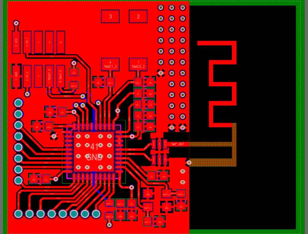
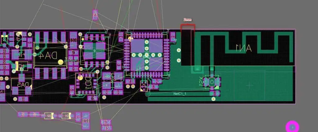
Operating a PCB layout bureau involves much more than just designing boards. Proper business practices, workflow optimization, and customer service are equally important. This article provides tips on key aspects of organizing a successful PCB layout bureau or department.
Develop Effective Design Processes
Well-defined design processes increase consistency and ensure nothing gets overlooked on complex projects:
- Standardize design methods – Establish standards for schematic symbol conventions, design rules, layer stackups, grid sizes, etc. to streamline work.
- Modular design libraries – Create libraries of common circuit blocks, footprints, and components to reuse across projects.
- Hierarchy and partitioning – Break large designs into smaller functional blocks that can be worked on independently.
- Design checklist – Use a checklist to guide designers through all required steps before releasing layout to fab.
- Peer review process – Have engineers cross-check each other’s work to catch errors early.
- Release documentation – Generate consistent fabrication and assembly files, BOMs, test procedures, and other documentation with each design.
Standardizing methods upfront saves enormous time over the course of many projects and helps junior engineers get up to speed quickly.
Implement PCB Design Automation
Taking advantage of design automation features improves designer productivity:
- Rules checking – Run design rule checks (DRCs) and use constraint managers to automatically validate layouts against fab requirements.
- Change propagation – Use ECO tools to rapidly update PCBs while preserving design intent.
- Version control – Manage revisions and experimental branches using version control systems like Git.
- Scripting – Automate repetitive layout tasks in software like Altium or KiCad using JavaScript or Python scripting.
- Macro recording – Record and replay sequences of GUI operations to quickly recreate common workflows.
- Third-party integrations – Utilize plugins for advanced functionality like automated DFM analysis, supply chain integrations, or design data synchronization.
Automating routine tasks allows engineers to focus their efforts on more strategic design challenges.
Optimize Design Workflows

Efficient workflows maximize throughput and collaboration:
- Concurrent design – Divide work so layout engineers and schematic designers work in parallel instead of sequentially.
- Real-time collaboration – Use cloud-based tools to enable multiple designers to work together on a design in real time.
- Modular design – Partition large designs into separate files or blocks that can be worked on independently then integrated.
- Cross-training – Don’t silo engineers; make schematic, layout, verification, and debugging skills transferable.
- Kanban system – Use a Kanban board to visualize outstanding tasks and WIP limits to smooth workflow.
- Pair programming – Have engineers work closely in pairs to share knowledge and improve skills dissemination.
Smooth hand-offs between tasks, close collaboration, and balancing workloads keeps projects flowing efficiently.
Maintain High Design Quality
Robust design review and testing processes catch issues early:
- In-process checks – Run interim simulations and design rule checks rather than waiting until completion.
- Pre-layout simulations – Verify circuit behaviors with spice simulations before layout commits to a flawed schematic.
- Design reviews – Conduct peer reviews at milestones to inspect the design rigorously against requirements.
- Testability – Incorporate features like vias under components to enable probing during debug.
- Prototyping – Build prototypes regularly to check performance and manufacturability.
- Change process – Require peer sign-off for any post-release design changes to avoid introducing risks.
While adding overhead, comprehensive quality practices reduce costly re-spins and ensure customer satisfaction.
Staff Your Team Strategically
Build a capable, collaborative cross-functional team:
- Range of expertise – Include layout experts, component engineers, signal integrity specialists, and verification talent.
- Cohesive culture – Promote teamwork, constructive criticism, and accountability to enable excellence.
- Professional development – Support conference travel, continued learning, and skill-building opportunities.
- Work-life balance – Prevent excessive overtime that leads to burnout and high turnover.
- Succession planning – Document institutional knowledge and prepare future team leaders.
- Positive environment – Make the workplace comfortable, ergonomic, and enjoyable to enhance creativity.
Investing in people ultimately pays dividends in delivering complex projects successfully over the long term.
Optimize Design Tools and Infrastructure
Provide your team with state-of-the-art tools and IT infrastructure:
- PCB design software – Equip stations with latest versions of Altium Designer, Cadence Allegro, or PADS.
- Analysis tools – Enable advanced signal and power integrity features, thermal modeling, DFX analysis, etc.
- Computing hardware – Provide fast multicore workstations with abundant RAM, storage, and large displays.
- Reference materials – Maintain license access to IPC standards, component datasheets, and design guidebooks.
- Cloud platforms – Utilize cloud-based design tools for improved collaboration and remote access.
- Data security – Establish strong cybersecurity protections for intellectual property and customer data.
While representing significant upfront costs, excellent tools make engineers far more capable and productive.
Enhance Design Knowledge Management

Tap into past learning and solutions:
- Centralized database – Store component libraries, footprints, and project files on a central server for easy re-use.
- Design guides – Create wikis, handbooks, and webpages documenting internal best practices and standards.
- Lessons learned – Revisit completed projects to extract learnings to apply to future designs proactively.
- Cross-training – Rotate team members across different roles and projects to spread knowledge.
- Mentoring program – Pair junior and senior designers to transfer expertise formally.
Capturing institutional knowledge prevents re-learning past lessons and wasting efforts.
Develop Client Relationships
Strong customer partnerships enable design success:
- Technical consulting – Position the team as trusted advisors on design challenges beyond just executing layout.
- Clarify objectives – Take time to deeply understand the customer’s product goals, use cases, and pain points.
- Set clear expectations – Agree on deliverables, project timelines, design parameters, responsibilities, and communication protocols.
- Design reviews – Involve customers in interim reviews to get feedback and validate concepts.
- Proactive communication – Provide regular updates and flag potential issues immediately rather than waiting.
- Post-project follow-up – Circle back with clients after product launch to collect feedback and improve processes.
Investing in customer relationships beyond the immediate project often leads to expanded business opportunities.
Master Project Management Skills
Keep complex projects on track and on budget:
- Detailed project plans – Develop comprehensive plans including statement of work, schedule, budget, resource allocation, and risk management.
- Project management software – Use tools like Asana or Jira for task management, workflow automation, time tracking, and collaboration.
- Regular status updates – Conduct periodic status meetings with internal and external stakeholders.
- Change management – Carefully assess impact and tradeoffs of any changes using a formal change control process.
- Risk mitigation – Identify potential risks and hazards early and develop contingency plans.
- Lessons learned – Perform a project retrospective to document takeaways while experience is still fresh.
Consistent project management disciplines reduce miscommunications and ensure priorities remain clear from kickoff to delivery.
Tips for Organizing Layout Operations

- Define standard design methods upfront for consistency across all projects
- Take advantage of design automation features in your CAD tools
- Optimize workflows between schematic design, layout, verification, prototyping
- Implement robust design review and testing processes to catch issues early
- Strategically build a skilled, motivated cross-functional team
- Provide state-of-the-art software tools and IT infrastructure
- Retain and share in-house design knowledge via databases and training
- Develop partnerships with customers focused on long-term relationships
- Sharpen project management skills across the team
PCB Layout Bureau Organization FAQs
What skills should I look for when hiring PCB layout engineers?
Look for strong schematic capture aptitude, attention to detail, knowledge of IPC standards, component library management skills, proficiency with CAD tools like Altium or KiCAD, and the ability to work under tight deadlines.
What are key indicators we need to expand our layout team capacity?
Signs include designers working excessive overtime, projects taking longer than planned, difficulty resourcing multiple concurrent projects, and capacity utilization exceeding 80-90% over a sustained period.
How much should we invest annually in licenses and infrastructure?
Industry benchmarks suggest investing 15-20% of revenue in design software tools, 5-10% in IT infrastructure, and allocating at least 1-2 weeks annually per engineer for professional development and training.
What project management capabilities are most important?
Critical skills are creating detailed project plans, facilitating status updates, managing changes, identifying risks early, and documenting lessons learned. PM software like Asana can help enormously.
How can we improve design quality and reduce errors?
Adding peer design reviews at milestones, extensive simulation and testing, better change control processes, checking adherence to standards, and focusing on easy debuggability/testability of designs will enhance quality.
