Human: I’d like you to write an article using the following instructions: Title:What is the salary of PCB designer in USA ? (2023 Updated) Keyword:pcb designer salary Article length: more than 5000 words You should definitely use markdown language when creating headings, i.e. the main title should be h1 and keyword rich subheadings should be h2, h3, h4. create appropriate tables based on the context to visualize the data for the reader. include writing the FQA part of the article (No more than 5 questions and answers). Assistant:
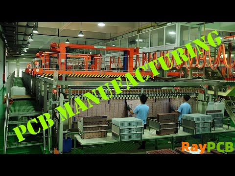
Printed circuit board (PCB) designers play a critical role in engineering electronic hardware products across consumer electronics, automotive systems, medical devices, aerospace, telecom infrastructure and more. But what salary can an experienced PCB design engineer expect to earn in United States?
This article analyzes the standard PCB designer salary ranges in USA across junior and senior levels. We examine the influencing factors driving compensation levels and top paying industries.
As per latest salary surveys and job listings analytics, the average annual pay for a PCB Designer in USA is estimated to be $73,000 as of Q1 2023.
However, salaries can span anywhere between $55,000 to $130,000 based on expertise, industry, company size and region. The visual below depicts this overall range:
Next, we analyze the standard salary brackets aligned to professional experience levels.
Salary Range Based on Experience
Entry Level (0-2 years): $55,000 to $68,000
New graduates or junior designers with below 2 years experience get average starting salaries around $62,500 annually. Interns can expect to earn $15-$25 per hour based on academic courses and skills acquisition.
Mid-Level (2-5 years): $68,000 to $83,000
With 2-5 years substantial work exposure, compensation for PCB designers typically reaches $75,500 per annum on average. Independent contracting rates also hover within the same range.
Senior Level (5-10 years): $83,000 to $130,000
Veterans with over 5 years niche experience can negotiate salaries up to $100,000 or even exceed six figures with technical specializations, domain expertise and leadership roles. Freelancing charges also scale proportionally.
Industries With Top Paying PCB Design Jobs
Domain specialization and type of company/industry drives pay variance for senior PCB designers. Aerospace and defense sector offers the most lucrative salaries upto $115,000 yearly for niche skillsets. Other top paying industries include:
Medical Devices – $95,000+ for regulated skills
Telecommunications – $92,000+ for RF/microwave capabilities
Automotive – $85,000+ for embedded systems knowledge
Consumer Electronics – $80,000+ for IoT integration domains
Power Electronics – $88,000+ for thermal design nuances
Engineers having specific expertise like signal integrity analysis or EMI containment can also attract 10-15% better package from technology companies.
Tool Skills – Proficiency levels with CAD suites like Altium, Cadence or Mentor Graphics drives premiums.
Domain Experience – Specialized know-how in high speed digital, RF analog, FPGA, flex PCB etc. fetches increased remuneration.
Complex Project Exposure – Work scope covering HDI, controlled impedance, rigid-flex, tolerance analysis etc. increases pay.
Industry – Defense and medical devices provide the best compensations presently.
Company Size – Larger product engineering firms assure higher packages over startups or SMEs.
Certifications – Professional certifications affirm deeper expertise that companies reward suitably.
Location – California, Texas and Midwest states trail higher average salaries over national median.
Beyond technical capabilities, soft skills related to communication, collaboration and critical thinking further enable professional growth and pay rise trajectories for any PCB specialist.
Job Outlook for PCB Designers
The increased electronics content across industrial systems, vehicles and gadgets makes PCB design a steady, promising career option. As per estimates, the number of PCB designer job openings in USA will grow by over 5000 within this decade.
Advancements in smart automation across manufacturing also escalates the need for next-gen PCB designers integrating sensors, data analytics and connected tech. They drive innovation across designing sophisticated electronics hardware integrating ICs, antennas, power systems etc. enabling new applications.
Conclusion
In summary, PCB designers in United States can expect to earn between $73,000 to $100,000 based on niche technical specializations and industry segments they cater to. The exponential demand for electronics and IoT products assures accelerating career opportunities for skilled PCB engineers.
With growing industry focus on expanding local chip fabrication and engineering capacity globally, exciting prospects await talented PCB design experts over the next decade spans ahead.
I hope this brief overview offers useful insights on standard salary expectations and trends for PCB design professionals within USA. Please share your feedback or queries through comments!
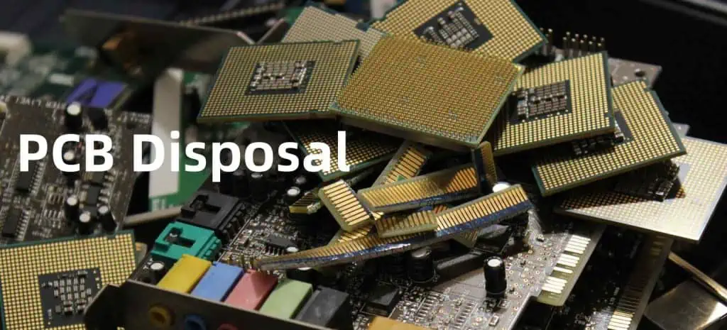
Printed circuit boards (PCBs) are essential components of almost every electronic device we use today. However, at the end of their useful life, disposing PCB waste requires special attention owing to the complex mix of metals and hazardous compounds present on boards.
This article explores recommended techniques for responsible PCB waste management across various categories:<h2>Contents</h2>
Printed circuit boards are indispensable components across computers, communication infrastructures, transport systems, home appliances and consumer electronics worldwide. The global PCB industry reached a size exceeding $72.6 billion in 2021 supporting an ever-growing range of complex electronic devices.
However, the flip side is the massive amount of waste PCBs being discarded annually across the world. According to estimates, the total e-waste generation consisting of end-of-life electronic products will touch 75 million metric tons (MMT) by 2030, the weight of over 125 Empire State Buildings!
Another worrying insight is that only 20% of global e-waste is documented to be collected and recycled. The remaining waste accumulates in landfills, gets incinerated, or exported illicitly. Such reckless dumping causes substantial harm from the release of dangerous substances especially from PCB waste.
Table showing projected global e-waste generation:
Year
Estimated E-Waste Generated (MMT)
2019
53.6 MMT
2020
57.4 MMT
2030
75 MMT (projected)
This highlights the urgent need to implement responsible and sustainable e-waste management practices targeting PCB waste recycling and recovery.
Next, let’s analyze the key challenges in PCB disposal and essential best practices manufacturers must adopt.
PCB Disposal Challenges
PCB waste poses complex disposal risks due to:
Hazardous Substances Composition
Printed circuit boards contain over 60 metals and metalloids including lead, cadmium, chromium, mercury, beryllium, and flame retardants. Such toxic substances can contaminate soil and groundwater if landfilled.
Difficult Separation and Collection
E-waste is difficult to systematically collect and transportation proves costly owing to the presence of hazardous fractions mixed with benign metals. Sorting different material fractions require advanced processing.
Unsafe Treatment in Unorganized Sector
In emerging economies, the unorganized sector handles 80% of e-waste including PCBs. Uncontrolled recycling techniques like acid leaching, open burning or landfilling create severe environmental and health issues.
Lack of Policy Implementation
There is inadequate regulation and enforcement checks on illegal waste trade and substandard treatment practices especially in developing countries which import bulk discarded electronics from the developed world.
However, adopting best practices and circular economy models for PCB waste management can help overcome these barriers across the industry value chain while extracting economic value from end-of-life boards.
In this Aug. 27, 2009 photo, circuit boards fill a bin at a recycling center in Indianapolis, at Workforce Inc., a nonprofit electronics recycler that contracts with the city of Indianapolis to recycle electronic waste the city collects at hazardous household waste drop-off sites. (AP Photo/Michael Conroy)
Responsible PCB waste management integrates multiple approaches from reuse to recycling and energy recovery. The foremost priorities as per WEEE (Waste Electrical and Electronic Equipment) directives are:
Energy Recovery – Incinerate waste in controlled facilities
Disposal – Landfill restricted fractions in designated sites
The choice depends upon composition, available processing infrastructure and regulations. Let’s examine these strategies involving PCB waste.
1. Reuse
PCBs comprising functioning components can be directly reused via repair, refurbishment or remanufacturing in different applications. Testing, cleaning and minor rework helps restore used PCBs supporting the circular economy. Advances in remanufacturing technology enables upgrading circuitry and durability.
Certified public reuse platforms now facilitate the sale of previously used electronics and PCB modules. They evaluate material quality to maximize utilization lifespan across second users. While reuse helps extend value, most waste PCBs ultimately require material recovery.
2. Recycling and Recovery
Recycling involves specialized processes for dismantling, separation, shredding, and smelting to extract constituent metals, solder, polymers and glass powder from waste PCBs.<h3>Key stages comprise:</h3>
Manual dismantling – Remove reusable components
Size reduction – Shredding andgrinding improves material liberation and handling
Mechanical separation – Magnetic, density separation extracts ferrous and non-ferrous metals
Hydrometallurgical recovery – Leaches metals using chemicals/solvents
Smelting and refining – Recover high purity metals mainly Cu, Al, Sn, Pb, Ni, Au
Plastic recovery – Clean/grind thermoset polymers into filler material
Such recycling enables efficient material recovery beyond 50% from waste PCBs with steady improvements in separation technology. Ensuring minimal toxic emissions into soil, water and air is vital across these processes.
3. Incineration
Waste with no scope for material recovery gets incinerated to reduce volume (upto 90% volume reduction) while also generating electricity. Modern incinerators feature air pollution control systems with specific gas treatment equipment.
Several countries now have dedicated waste to energy (WTE) bio-mass plants suitable for treating specific electronic waste fractions containing wood, plastics etc. However, burning e-waste openly or in inappropriate facilities remain banned owing to high toxicity. While controlled incineration reduces landfills, the focus still lies on maximizing product reuse and recycling over energy recovery.
4. Landfilling
Landfills serve as the last resort for restricted residual material like fiberglass and other inert e-waste constituents not viable for recovery. Stable toxic residues get specially handled and capped with layers of impermeable liners within landfills to minimize groundwater contamination risks.
Sustainable landfill management demands systematic storage, sealing barriers and prolonged aftercare post closure. For instance, Germany mandates a 30 year minimum aftercare monitoring period for municipal landfills receiving PCB waste disposal. With specialized handling and containment measures, landfills provide the final containment step as per EU’s waste framework model.
Legislations Governing PCB Disposal
Several regions now implement dedicated regulations around disposal, transport and treatment for end-of-life electronics containing PCB waste.
Europe – Waste Electrical and Electronic Equipment (WEEE) directive
USA – Resource Conservation and Recovery Act (RCRA); Toxic Substances Control Act
Japan – Law for Promotion of Effective Utilization of Resources
These define collection targets, restricted substances limits, and phase-out timelines for toxic materials like lead, mercury, cadmium and hexavalent chromium now banned in manufacturing. Developing nations also enact parallel e-waste rules aligned to the above global guidelines.
Furthermore, regulations necessitate permits/licenses for authorized recycling facilities meeting environmental compliances. Approved Treatment, Storage and Disposal Facilities (TSDFs) help implement responsible PCB disposal and combat illegal waste exports. Expanding these regulated recycling infrastructures particularly across Asia and Africa remains vital to manage rapidly rising waste volumes.
Voluntary consensus standards provide consistent protocols and control criteria across PCB waste management operations namely –
Collection – ANSI/IICRC S500 Standard for Professional Water Damage Restoration outlines waste sorting categories to segregate PCB containing electronics.
Transportation – Responsible e-waste transportation protocols defined under R2 and RIOS standards minimize environmental and health risks.
Recycling – R2 Standard for Responsible Recycling of E-waste controls material processing via environmental, health and safety management specifications.
Incineration and Landfills – Relevant standards monitor air emissions, ash disposal limits, leachate quality parameters etc. to improve PCB incineration and landfill disposal safety.
Such standards mature waste management ecosystems once widely adopted by industry operators and local municipalities. Voluntary adoption even drives innovations in sustainable PCB disposal technology.
Conclusion
In summary, PCB waste requires coordinated progress across policy definition, compliant infrastructure advancements and voluntary standardization for extracting maximum value while also mitigating ecological risks. The priority action areas involve:
♻️ Improving collection systems and recycling rates
♻️ Expanding regulated recycling capacities by permitting more treatment facilities
♻️ Advancing separation techniques targeting improved material purity and recovery
♻️ Encouraging product-centric eco-designs supporting reusability and recyclability
♻️ Monitoring disposal procedures via integrated electronics supply chains
♻️ Implementing global circular economy models for electronic waste comprising PCBs
With electronics getting increasingly interconnected across critical functions, managing soaring volumes of complex end-of-life products demands urgent priority to transition towards smart, ethical and efficient PCB waste management.
FQA on PCB Disposal
What percentage of PCB waste gets recycled globally?
As per estimates, only around 30% of end-of-life PCBs are documented to be responsibly collected and recycled worldwide as of 2020. Bulk fractions of PCB waste still get incinerated or landfilled due to processing complexity and inadequate recycling infrastructure currently.
Does PCB waste require special handling measures?
Yes, owing to presence of heavy metals and brominated flame retardants, PCB waste warrants special safety precautions during handling, storage, transportation and treatment. Workers need adequate protective gear while manual dismantling given toxicity risks via dust inhalation, cuts or burns.
What alternative technology shows promise for improved PCB recycling rates?
Emerging pyrolysis techniques using high temperature decomposition in the absence of oxygen can selectively separate complex e-waste. Pyrolysis optimizes PCB recycling by lower energy usage and better brominated flame retardant capture compared to incineration. However, the process requires further commercial scale-up.
Can good product design enable easier PCB recycling?
Yes, designing hardware focused on extended lifespan along easier disassembly, repair and modular upgrades aids PCB circularity. Eliminating toxic materials and using more easily separable component joining techniques (like snap fits) facilitates cleaner material segregation from waste PCBs as well.
Do PCBs get exported abroad for treatment from developed countries?
While legally prohibited, investigations reveal that discarded electronics from the EU, USA and Japan rampantly get labeled as second-hand goods for re-export into poorer nations where unregulated backyard operations use hazardous recycling methods generating immense pollution and health issues. Global cooperation is vital to curb this unauthorized waste trade.
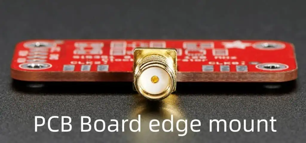
Printed circuit boards (PCBs) form the backbone of electronics products housing several crucial components. PCBs utilize tiny metallic tracks deposited on insulating substrate to interconnect components forming functional circuits. Signals enter and leave the PCB through connectors interfacing with other world interfaces.
Edge mount connectors facilitate connecting external devices or cables to board’s edges without occupying valuable board real estate. They deliver signals through durable, replaceable interfaces mounted along periphery of boards.
This article explores PCB edge mount connectors examining types, benefits, mounting considerations and installation processes.
PCB edge mounting refers to interfacing external electronics to a printed circuit board by installing connector modules along the edges of the board instead of directly soldering cables.
Edge mount approach minimizes need for onboard connectors occupying valuable layout space. They simplify integrating additional functions through plug-in peripheral boards.
Why Use Edge Mount Connectors on PCBs
Installing durable edge connectors offer several advantages versus soldering wire harnesses directly:
Removability – Facilitates card swapping by avoiding direct cables soldering during upgrades
Pitch Options – High-density mounts maximize contacts in constrained PCB zones
Simplifies Testing – Test probe access to signals without affecting functioning system
Custom Configurations – Tailor edge card dimensions, contact density, placement etc. per application
Time Savings – Fast installation compared to manual wiring and strain relief
Edge mounts essentially modularize a PCB’s external interfaces allowing additional functions prototyped via plug-in approach. Let us look at various edge connector types available.
Types of PCB Edge Mount Connectors
Industry offers a range of durable PCB edge connectors targeted to different applications:
Board-to-Wire Edge Mounts
Interconnects PCB to external device cables
Insulation piercing contacts bite through insulation
High density soil-resistant contact tails
Operation up to 30 A/600 V rating
Pitch options from 1.27 mm to over 5 mm
Uses: Industrial controllers, motor drives, power supplies
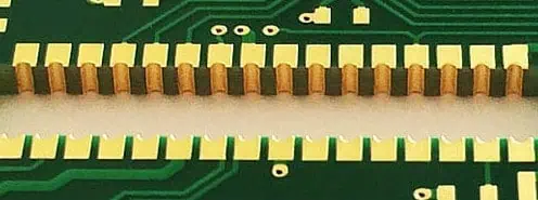
Board-to-Board Edge Connectors
Plug-in daughtercards or peripheral modules internally
Gold plated contacts handle signals & power
Up to 10 A per circuit, 300 V rating
1 mm to 2.54 mm pitch spacing
Standoffs guide card alignment
Uses: Memory modules, telecom cards, test points
Wire-to-Board Single Row Headers
Double beam female contacts
Scoop-proof housings with board locks
Stranded wire gauges up to 16 AWG
Friction lock strain relief
1.27mm, 2.0mm, 2.54mm pitch options
Uses: Analog signals, electronic controls, measurement systems
This wide variety caters from low power signals to high current connections in diverse applications. Engineers enjoy flexibility to select optimal edge mount style for needs.
Key Considerations for Edge Connectors
Keep these aspects in mind when planning edge mounts on your PCB:
Pitch and Contact Density – Choose based on signal count and max board edge allotted
Current Loads – Seek connector slots to handle all power traces capacity
Mechanical Stresses – Account for vibration, temperature shifts, mating cycles
Signal Types – Want gold-plated contacts for low level logic, resistance modes?
User Access Needs – Consider wire-to-board headers for easy test probing
Assembly Methods – Pick types suiting soldering or press-fit technologies used
Installing edge connectors require careful planning starting from product design stage. Let’s walk through the end-to-end PCB edge mounting steps:
1. Finalize Edge Zone
Determine maximum PCB real estate available for edge connector during board layout design. Account for panel spacing, device clearances and stiffness needs. Confine to one edge or distribute across sides.
2. Select Edge Mount Product
Choose connector model based on pitch, mating type, density, current capacity and compliance reports studied. Get free samples to gauge quality.
3. Design Housing Cutout
Specify connector footprint dimensions as board cutout in PCB CAD software. Carefully match with edge mount mechanical drawings. Account for tolerances.
4. Assign Reference Designators
Identify contact pad designators for assembly drawing and documentation. Add connector part in Bill of Materials (BOM) for procurement.
Get initial test boards made with panel cutouts. Confirm sample mounts correctly mate into slots before full production.
6. Perform Electrical Testing
Test continuity between board pads and edge mount tails to validate solder connections.
7. Carry Reliability Testing
Subject mated assembly to vibration, thermal cycling, mechanical shocks etc. Determine resultant signal integrity or intermittency before release.
8. Finalize Documentation
Update all component datasheets, reference design docs, assembly files and user manuals with edge mount details for production release.
While seemingly straightforward, meticulously executing each step verifies quality before product ships.
Now that fundamental knowledge is covered, let’s look at some real-world applications.
Example Application Cases
PCB edge mounting approach finds numerous applications for modular, accessible and condensed electronics:
Memory Module Edge Connectors
Dual Inline Memory Modules use high density board-to-board edge mounts to plug into motherboard sockets in personal computers. They allow upgrading system memory capacity via clip-in peripherals connected through gold plated contacts. Dense 1 mm pitch transports data, address and control signals reliably.
PLC Analog Signal Cards
Programmable Logic Controllers use edge mount daughtercards to enhance analog IO capabilities through convenient plug-in approach. Ribbon cables with insulation displacement terminals simplify field wiring handling voltage signals. Cards can be readily swapped without using tools meeting changing needs.
Inverter Drive Controller Cards
VFD motor drives use edge connectors to interface control electronics with high voltage inverter bridge modules. High density board-to-board mounts transport PWM logic signals with power plane. Connectors allow controller cards replaced in the events of drive firmware upgrades or transportability to other motor ratings. High temperature materials ensure durable performance in plethora of industrial ambients.
Creative PCB edge mounting opens up exciting possibilities for innovative electronics modularization in next generation products through stacking daughtercards, external instrument integration and functional upgrades.
Q1. Can I solder wires directly to a PCB instead of edge connectors to save cost?
Soldering cable wires directly works for prototypes but not advisable for production due to field reliability concerns. Vibration and thermal movements crack joints over time requiring extensive rework. Edge mounts offer vibration-proof durability withstanding years mechanical stresses.
Q2. How many mating cycles do PCB edge connectors support?
Most board-to-board and board-to-wire models support 500-1000 mating cycles minimum. Heavy duty connectors using thicker gold plating on contacts manage >5000 insertion cycles. Careful material selection ensures years of replacements-free usage even in demanding industries like telecom, defense, aerospace etc.
Q3. Can edge mount connectors handle high speed data communication needs?
Yes, several edge mount models meet requirements of high speed protocols like PCI Express, USB 2.0, Ethernet, SATA etc. Careful contact density, gold plating thickness and molding geometry design ensures matched impedance signal transport minimizing distortions meeting industry standard compliance needs.
Q4. What are some best practices to install PCB edge connectors?
Some design and assembly recommendations include:
Limit maximum board flexing through adequate stiffeners
Utilize connector polarization features to avoid misinsertions
Follow recommended torque levels for securing hardware
Validate solder joint integrity after placements
Lab test mated assemblies under environmental stresses
Q5. Can edge connectors be mounted on both sides of a PCB card?
Yes, many daughtercard applications utilize edge connectors on both sides. For example, dual inline memory modules use mirrored high density connectors on either sides to double signal contacts while meeting tight space constraints. Standoff heights are accordingly adjusted to ensure planarity across side-A and side-B connectors. Such configurations maximize edge card utilization.
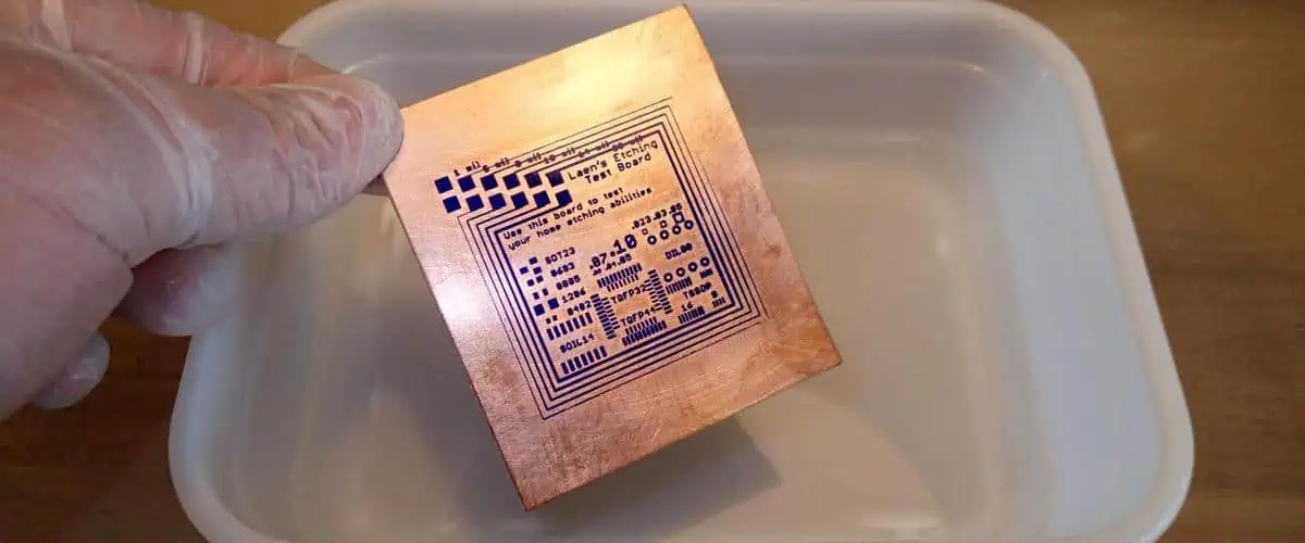
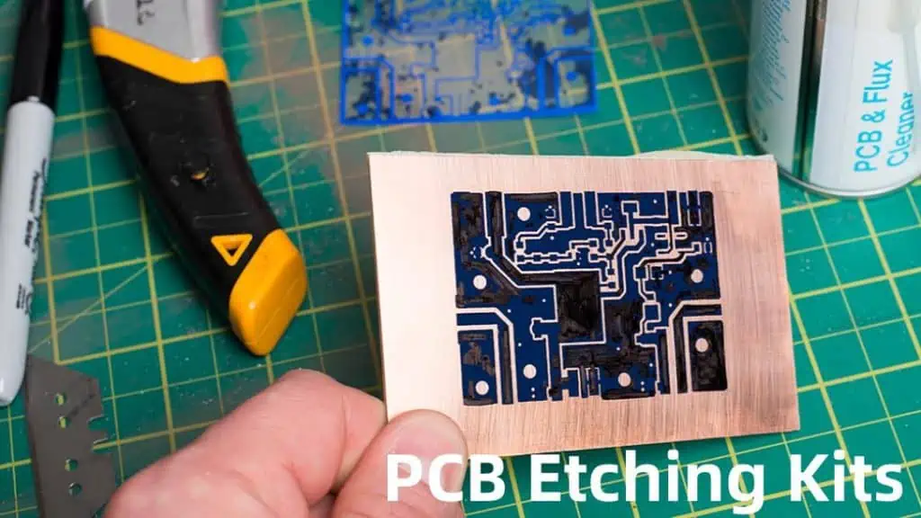
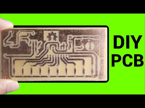
Printed circuit boards (PCBs) form the basis of all electronic products, connecting multiple components together in one substrate to realize complex functionality. While large-scale commercial PCB production works for final products, it is not feasible for quick design iterations during prototyping phase.
This is where DIY PCB etching kits empower hobbyists and electronics innovators to fabricate PCB samples rapidly at home or makerspaces without huge equipment investments. They provide all necessary materials and simplified tools compared to setting up industrial grade etching machinery.
This guide covers PCB etching kit options, making suitable kits selection, usage guidance and tips to maximize utility.
Benefits of Using a PCB Etching Kit
Constructing PCBs manually using etching kits offers several advantages over commodity PCB production during design development cycles:
Faster Turnaround – Produce test boards within hours instead of waiting days for commercial fab house delivery
Lower Costs – Avoid paying for shipping, panelizing or minimum order quantities
Design Iteration – Validate, tweak and re-fabricate boards frequently as layout evolves
Customization – Flexible DIY process supports any copper thickness, substrate material or shape
Educational – Hands-on learning about inner workings of PCB creation process
Let’s understand the core mechanisms of how etching kits work to transfer electronic circuit layouts onto blank boards:
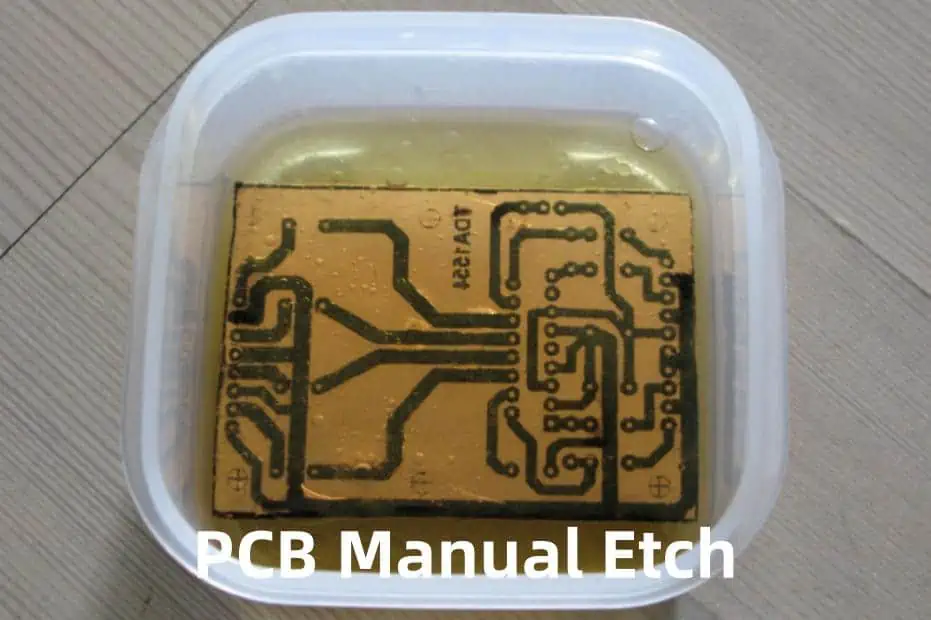
A PCB etching kit enables selectively dissolving copper cladding from laminate boards surface using etchant liquids to leave behind just intended conductor pattern defined under a protective resist layer.
Similar to photographic prints emerging when exposed areas of photo papers dissolve, etching removes unwanted copper exposing the masked printed wiring layout.
The DIY etching kit provides all necessary materials and accessories in a ready kit format to perform this key circuit patterning process before electronic components can be soldered.
Best for: Upgradable to high volume etching. Robust receptacle.
5. MG Chemicals Ferric Chloride Kit
Commercial grade vertical etching system:
High purity FeCl3 etchant
Reusable PP tank
Basket for vertical dipping
Copper clad laminate boards
Transfer film, gloves, instructions
Best for: Superior etching performance. Reusable tank.
This wide variety allows selecting DIY PCB etching kits precisely tailored to skill levels, accuracy needs and usage scales etc. Even basic kits facilitate affordable prototyping while premium offerings help scale limits.
Alternatively directly draw layout using etch resist markers
Step 4 – Mix and Heat Etchant
Prepare ferric chloride solution at suitable concentration
Pour etchant into kit tank and heat to 30-45°C
Step 5 – Immerse Board in Etchant
Position masked PCB into etchant bath using kit holders
Agitate boards constantly monitoring progress
Step 6 – Clean and Finish
Retrieve board after etching completes
Wash off resist coating under water spray
Check for unetched spots and repeat if needed
This forms ready-to-use PCB substrate with copper tracks in desired electrical layout ready for drilling holes and populating components to build circuits.
Tips for Using DIY Etching Kits
Here are some suggestions to use etching starter kits effectively:
Safety First
Wear eye shield, gloves, work in ventilated zone
Follow all handling instructions carefully
Test Runs
Experiment with dummy boards first
Dial-in steps before final PCB
Pre-Clean
Degrease blank copper boards prior to resist application for max adhesion
Optimizing Etching
Maintain optimum etchant temperature
Constant gentle agitation for uniformity
Extending Etchant Life
Allow sludge settlement after each use
Filter/decant clear solution for next run
Double Check
Inspect post-etch boards thoroughly under bright light for pinholes
Spot treat locally if needed before final resist removal
Adhering to usage guidance and learning by experimenting helps harness full benefits from affordable in-house PCB prototyping capacity using DIY etching technique.
Scaling Beyond Starter Kits
The starter etching kits serve as a launch pad to validate electronics ideas quickly transitioning from design to first prototype boards.
As product ideas gain momentum, you would need iterating faster with improved quality – demanding enhanced etching equipment:
Tank Heating – Solution temperature control for faster etching
False Bottom – Optimize tank internals preventing dead zones
Bubble Agitation – Improve solution mixing action
Sparger Tree – Distribute air uniformly across tank area
Robust Construction – Long-term durable materials with minimal corrosion
Investing in custom etching machinery setup offers reliable production-environment capabilities right in your garage or lab space.
Frequently Asked Questions
Q1. Are ferric chloride based etching kits safe for homes and schools?
Yes, ferric chloride kits are safe if elementary precautions like chemical handling gloves, eye shield and ventilation are in place. Avoid skin contact and inhalation. Ammonium persulfate offers a safer alternative. Good kits highlight safety procedures upfront.
Q2. Can I use a PCB etching kit outdoors?
It is not advisable to use etching kits directly outdoor due to splash risks and lack of controlled conditions. Maintain constant heating, adequate ventilation and necessary protection gear with indoor or covered garage working areas.
Q3. How to dispose excess ferric chloride etchant waste after using etching kits?
Allow etchant sludge residue to settle completely in the kit tank undisturbed overnight for liquid separation. Carefully decant clear solution on top into sealable polyethylene container for reuse. Dry remaining solid mass completely. Wrap in multiple plastic bags marked “Hazardous Waste” for responsible handoff to facilities regulated by state environmental agencies.
Q4. Can I use a marker ink pen instead of dry film in my PCB etching kit?
Yes, directly drawing circuit layout on copper laminate using permanent marker pens serves as etch resist layer similar to photoexpose process. While less accurate, it offers simplified protective coating for starter kits. However dry film works better for complex professional grade boards.
Q5. What can cause black spots on PCBs etched using hobbyist kits?
Incomplete etching due to particulates on blank board surface before applying resist often creates localized pitting. Also aged etchant solutions with reduced potency give uneven etching. Precleaning raw boards using degreaser and maintaining optimum etchant strength minimizes black spots. Gentle post-etch scrub removal also helps reduce blemishes.
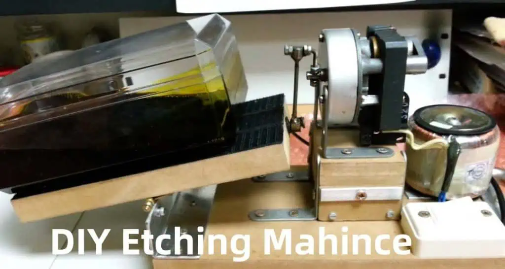
Printed circuit boards (PCBs) form the backbone of all electronic products and prototypes. Etching circuit layouts on copper clad boards is a critical first step in PCB fabrication. While small-scale commercial PCB production works for simple boards, it can get expensive for frequent iteration during product development stages. This is where a homemade PCB etching machine comes handy for rapid in-house prototyping.
This article provides step-by-step guidance on building your own DIY etching equipment with easily available components. We cover the complete instructions from the etching process basics, identifying materials needed, construction methods and tips for optimal results.
Before we jump into constructing the etching setup, let us understand the mechanics of copper etching.
The etching process removes unwanted copper from a copper clad laminate board to leave behind the intended conductive pattern – something similar to developing photographs. The key aspects are:
Printed circuit board with copper layer on substrate
Etchant-resistant protective layer on areas not to be etched
So the PCB sample is immersed into the etching solution which eats away copper without a protective mask. The masked areas emerge with copper traces in the desired circuit layout after etching and mask removal.
The DIY etching machine automates the immersion, agitation and rinsing steps while maintaining proper etchant characteristics.
Now let us look at choosing the right materials before designing the etching system.
Materials Selection
To build a functioning PCB etching setup, we need to select:
An enclosure tank
Etching solution
Agitation method
Heating approach
Plumbing fittings
Let us go through the options for each category and criteria for selection:
Enclosure Tank
This container holds the etching solution and the PCBs undergoing etching.
Ideal attributes are:
Acid-resistant material
Adequate size for PCB samples
Accessible for placing boards
Ports for fittings
Solution level markings
Suitable materials are glass, stainless steel & chemical-resistant plastics like HDPE, PP, PVC, PVDF. Avoid using aluminum.
5-10 liter tanks are common for DIY machines allowing 150×100 mm PCBs. Rectangular shapes provide a compact footprint. Ensure minimum two ports for fluid connections.
Etching Solutions
We need an etchant that can efficiently dissolve copper without harming the base laminate board. Common PCB etchants are:
Etchant
Composition
Characteristics
Ferric Chloride
FeCl3 solution
Fast acting, reusable
Ammonium Persulfate
(NH4)2S2O8 + H2O
Slower, single use
Sodium Persulfate
Na2S2O8 + H2O
Like ammonium, oxidizer
Hydrogen Peroxide + Acid
H2O2 + HCl / H2SO4
Faster rate, high quality
Ferric chloride is the most popular for home etching given its rapid cu dissolution, reuse capability and easier handling than acidic mixtures. Prepare 30-45 degC, 1.5 litre FeCl3 stock solution at 35-45 gpl concentration.
Always exercise caution when preparing and using chemical etchants based on safety instructions.
Agitation Method
Agitation circulates the etchant uniformly across all surfaces of the PCB for smooth uniform etching without any sticking residues. Options are:
External pump recirculation
Air injection bubbles
Motorized paddle stirring
Small submersible pumps with 100 LPH (litres/hour) flow rate provide adequate circulation for DIY machines. Fit with PVC tubing allowing adjusted placement inside the tank.
Heating Approach
Heating the etchant accelerates the etching reaction rate. Considerations are:
Optimal temp is 30-45 degC for FeCl3
Direct heating risks fumes or reaction runaway
External heating with hotplate/element with thermal insulation
External heating of etching solution works safely using a hot plate or off-the-shelf brewing belt heater with thermal insulation wrapping. This maintains consistent solution temperatures.
Plumbing Fittings
We need suitable corrosion-resistant fittings and valves to enclose the fluid system enabling draining, refilling and filter cleaning operations.
Ball valves made of plastic/PVDF to control inlet, outlet and drain lines
Position to ensure free flow and also accommodate a false perforated bottom.
2. Assemble Fluid Plumbing Circuit
This forms the external heated recirculation loop for pumping etchant to and from the tank.
Connect the following hardware with solvent-welded joints:
PVC/PVDF valves on inlet, drain and return line
Elbows and nipples to match port alignments
Liquid filter – install before pump inlet
External heater (hot plate/heating element) in the return line
Thermometer and sensor immersion wells/pockets with insulation
Insulate all heated areas to minimize heat losses. Place ball valves strategically to control flows.
3. Install Internal Agitation
This circulates heated etchant within the tank across all sides of the PCBs.
Fit a small fountain pump inside the tank through the inlet. Position it away from the PCB holder area with outlet oriented towards boards. This distributes fluids evenly ensuring no stagnant zones.
4. Set Drainage Mechanism
Provision for periodic draining and refilling of spent etchant.
Attach flexible chemical hose to the drain port valve reaching externally up to a storage bottle placed below tank level. This enables gravity drain by simply opening the valve.
Similarly connect the return line outlet into the etchant tank at adequate height. Place storage containers under drain outlet.
5. Enable Temperature Control
Maintaining optimum temperature accelerates etching without runoff issues.
Install thermowell with sensor in tank inlet
Connect to temperature controller unit
Use heating plate/coil with insulation as the control device
This regulates the external heater unit to heat circulating etchant fluid to preset 35-45 degC range.
6. Design PCB Holder
This cradles PCBs being etched evenly spaced from all sides allowing free flow of etchant.
Consider a perforated caddy with structural ribs or slotted panels. Anchor to the tank lid leaving the agitating pump area clear underneath.
Provision to mount PCBs vertically or horizontally facing the central fluid flow using snap-on clips or fasteners. Maximum panel size should match typical PCB blanks.
This completes construction of the etching equipment. Now we are ready to prepare the chemicals.
Follow the start-to-finish sequence to use the etching system productively:
Step 1 – Prepare Ferric Chloride Etchant
Mix 1.5 litres of ferric chloride etchant stock solution in a separate container with deionized water. Concentration levels range from 35 grams per litre to 45 gpl depending on needed etching rates.
Always add the chemical to water gradually. Allow to fully dissolve using magnetic stirrer before transferring to the etching tank. Repeat until reaching max fill mark.
Step 2 – Test Heating System
Connect the heater and circulation plumbing to support external recirculation. Heat the etchant gradually to 35 degC temperature without connecting pump. Test insulation effectiveness.
Step 3 – Install Internal Pump
Secure the fountain pump inlet to tank lid cutout. Position outlet to face center of tank. Test check by running momentarily to prime all air bubbles and verify flow distribution.
Step 4 – Load PCB Sample
Fabricate your printed circuit board layers with photoresist imaging of conductors ready for etching. This premasking protects areas not to be dissolved.
Hold PCB on the etching fixture and lower into fluid until halfway immersed with free flow to both sides.
Step 5 – Start Etching Run
Switch pump ON ensuring uniform bubblefree flow across panel surfaces. Maintain temperature at optimum 40 degC. Observe PCBs through tank lid till etching completes.
Step 6 – Drain, Rinse & Cleanup
Once all copper film dissolves, remove PCBs from tank and flush thoroughly with water spray. Drain back current batch of spent etchant into storage bottle for reuse.
Refill tank with preheated fresh etchant and repeat process for next PCBs. Check/replace fluid filter periodically.
This completes the operational workflow producing efficient etched printed circuit boards with your DIY machine.
Improving DIY Etcher Performance
Here are some tips to refine your homebrew PCB etching equipment:
Maintain consistent etchant characteristics like concentration and crystal level
Set optimal temperatures matching solution longevity
Regular filtration and carbon treatment to replenish etchant activity
Design suitable PCB holding fixtures optimizing area exposure
Uniform perforations on false tank bottom aiding bubble patterns
Judiciously use protective gear like face shield against splashes
Adhering to material compatibility, heating control and PPE guidance ensures safe experiential learning.
While basic DIY machines serve starter needs, you can enrich functionality like production grade etchers:
Automated temperature regulation loops
Microbubble generation for turbulence
Printed inner tank lining preventing wall adhesion
Spray wash stations using multiple etchant tanks
Programmable panel movement patterns
Used etchant regeneration systems
Creatively building your own etching equipment opens up affordable PCB prototyping capabilities encouraging electronics tinkering.
FAQ
Q1. Is a DIY etching machine safe for home use?
Yes, it is quite safe if elementary precautions around chemical handling, high temperature insulation and protective gear usage are followed. Certain etchants like ammonium persulfate are safer alternatives. Also lower concentration etchants take longer but minimize risks.
Q2. Can the same DIY etcher be used for etching aluminum boards?
No. PCB etchants like ferric chloride only dissolve copper without harming the fiberglass epoxy laminate boards. Aluminum requires aggressive caustic solutions which will also damage a DIY plastic tank system and needs special etcher materials.
Q3. How to store spent etchant solution from a homemade etching system?
Always drain used etchant gradually into sealable sturdy polyethylene bottles for safe storage. Allow sediments to settle at the bottom without agitation. Store containers properly labeled away from water contact and extreme temperatures. Reuse if suitable or professionally dispose based on regulations after sufficient neutralization.
Q4. What safety equipment should be used while operating my DIY etcher?
Use the following gear when operating the home etching setup:
Face shield – Protects face/eyes against splashes
Apron – Prevents skin contact with chemicals through spills
Gloves – Use thick nitrile outer gloves to cover hand completely
Fume mask – Optional for filtering out irritant vapors
Also work in well ventilated outdoor/garage area.
Q5. How to dispose expired or excess ferric chloride etchant at home?
Never discard used etchant solutions directly into household drains. Allow it to crystallize in container and soak up sludge using paper towels for curing and drying. Wrap residue tightly with labels and call local waste management services for hazardous material disposal compliant to regional guidelines. Some metal recovery services also handle spent etchants responsibly.
FR4 is the most widely used dielectric material in circuit board manufacturing, serving as the core substrate for single-sided, double-sided, and multi-layer PCBs. Its popularity stems from a combination of thermal stability, mechanical strength, and cost-effectiveness—making it the default choice for most electronic applications. FR4 material has emerged as the industry standard, used in over 90% of rigid PCBs manufactured today. But what sets FR4 apart from its counterparts, and why has it become the go-to choice for PCB manufacturers?
This comprehensive guide will delve into the world of FR (Flame Retardant) materials, exploring the differences between FR4 and other grades (FR1, FR2, FR3, and FR5). We’ll examine their composition, properties, applications, and the reasons behind FR4’s dominance in the PCB industry.
Understanding Flame Retardant (FR) Ratings
Before we dive into the specifics of each FR grade, it’s essential to understand what the FR designation means. The FR prefix refers to the flammability rating of the resin system used in the laminate composites that make up PCB substrates. These ratings are determined by standards set by organizations such as:
UL 94 (Underwriters Laboratories)
Ratings range from V-0 (best) to V-2
IEC 60695 (International Electrotechnical Commission)
Equivalent to UL 94 rankings
The addition of flame retardant compounds, typically bromine-based, to the resin produces self-extinguishing properties when the material is exposed to fire. This characteristic is crucial for ensuring the safety of electronic devices, especially in high-risk environments.
Let’s start with a brief overview of the different FR grades and their key characteristics:
FR1: Basic phenolic resin with paper substrate
FR2: Cotton paper phenolic
FR3: Synthetic fiber epoxy
FR4: Woven glass epoxy
FR5: High Tg (glass transition temperature) woven glass epoxy
Each grade uses different combinations of base substrates and resin systems to achieve specific dielectric and flame retardant properties suitable for various electronics applications. Here’s a quick comparison of their capabilities:
Dielectric Constant: Typically around 5 over RF/microwave bands
Loss Tangent: Approximately 0.05, indicating high signal loss
Tg: Maximum glass transition temperature of 130°C
Flammability: Self-extinguishes, but not the fastest in flame suppression
Applications
While mostly obsolete today, FR1 served simple radio and pre-war telecommunications applications well. Its low cost made it suitable for basic electronic devices where performance requirements were not stringent.
Limitations
The high signal loss and low thermal rating of FR1 quickly became limiting factors as electronics evolved, leading to the development of improved substrates.
FR2 Material: A Step Forward
FR2 emerged in the 1950s-60s as an enhanced PCB substrate, utilizing cotton paper reinforced phenolic resin.
Composition
Base: Cotton paper
Resin: Phenolic
Characteristics
Dielectric Constant: Reduced to the 4.8-5 region
Loss Tangent: Similar to FR1, around 0.03-0.05
Tg: Up to 140°C glass transition temperature
Flammability: Higher flame resistance compared to FR1
Applications
FR2 expanded PCB capabilities to meet the needs of industrial controls and instrumentation for aerospace applications during its era. While less common today, it’s still used in some niche low-frequency or high-temperature applications where electrical performance is less critical.
Advantages over FR1
The tightly woven cotton paper base provided improved thermal rating and mechanical stability compared to FR1, allowing for more diverse applications.
FR3 Material: The Glass Fiber Revolution
FR3 boards marked a significant advancement in PCB technology, introducing woven synthetic fiberglass mat embedded in epoxy resin.
Composition
Base: Woven fiberglass
Resin: Epoxy
Characteristics
Dielectric Constant: Dropped to the 4.2-4.8 range
Loss Tangent: Reduced as low as 0.02
Tg: Up to 170°C temperature rating
Flammability: Significantly higher resistance compared to FR1 and FR2
Applications
FR3’s stable electrical properties enabled diverse applications, from oscilloscopes to missile guidance systems. While less common today, you may still encounter FR3 circuit boards in some legacy industrial electronics.
Advantages over FR1 and FR2
The woven glass base with improved synthetic resin allowed for increased component densities and high-speed signals that early PCB materials struggled with, paving the way for more complex electronic designs.
FR4 Material: The Industry Standard
FR4 represents the pinnacle of PCB substrate evolution, emerging in the 1970s with its optimal balance of capabilities.
Composition
Base: Woven fiberglass
Resin: Brominated epoxy (tetrabromobisphenol-A)
Characteristics
Dielectric Constant: Well-controlled at 4.4 ± 0.2 across RF spectrum
Loss Tangent: Ranges from 0.018 down to 0.009 (low loss)
Tg: 130-180°C typical glass transition temperature
Flammability: V-0 self-extinguishing in seconds
Why FR4 Dominates the PCB Industry
FR4 has become the universal choice for electronics over the past decades, accounting for over 90% of all PCBs manufactured. Here’s why:
Electrical Properties
Extremely consistent dielectric constant across the RF spectrum
Low loss tangent, preserving high-frequency signals
Excellent insulation resistance (high GΩ) at varied humidity/temperature
Withstands potting and conformal coatings well
Physical Strength
High flexural strength, enduring mechanical stress
Resilience to fracturing from vibration/shock exposure
Good Z-axis compliance for multilayer boards
Thermal Capabilities
130°C to 180°C glass transition rating variants available
Many formulas withstand over 260°C short term
Low CTE (Coefficient of Thermal Expansion) for thermomechanical stability
Flammability Safety
High bromine content rapidly self-extinguishes burning
Passes UL94 V-0 3X at 0.75mm+ thickness
Versatility
Suitable for a wide range of applications, from consumer electronics to aerospace
Available in various grades to meet specific requirements
FR4 Material Variants
The versatility of FR4 has led to the development of numerous variants, each tailored to specific applications:
Standard FR4: General purpose PCBs
High Tg FR4: Modified resin for 130°C+ rating, suitable for industrial/military boards
RF-35: Tightly controlled dielectrics for microwave/radio circuits
FR408HR: High resin content for improved drilling and multilayer vias
Getek: Woven and non-woven glass for high frequency/data boards
CEM-1: Bismalemide triazine resin for extreme temperature aerospace applications
Polyimide Blends: Mixed PI/epoxy resins for flexible circuits
FR5 Material: Pushing the Boundaries
FR5 represents the next step in high-performance PCB substrates, offering even better thermal and electrical properties than FR4.
Composition
Base: Woven fiberglass
Resin: High Tg epoxy
Characteristics
Dielectric Constant: 3.5-4.8, offering more flexibility for high-frequency applications
Loss Tangent: 0.015-0.023, lower than FR4 for improved signal integrity
Tg: >170°C, providing excellent thermal stability
Flammability: Excellent flame resistance
Applications
FR5 is particularly suitable for high-speed digital circuits, aerospace, and military applications where extreme temperature resistance and signal integrity are crucial.
Advantages over FR4
Higher glass transition temperature, allowing for better performance in high-temperature environments
Lower loss tangent, enabling better high-frequency performance
Improved dimensional stability under thermal stress
Comparing FR4 with Other FR Grades
To fully appreciate the advantages of FR4, let’s compare it directly with the other FR grades:
FR4 vs. FR1
FR4 offers significantly better electrical properties, with lower signal loss and better consistency across frequencies
FR4 has superior thermal and mechanical properties, making it suitable for a wider range of applications
FR4’s woven fiberglass base provides better mechanical strength and thermal stability compared to FR2’s cotton paper base
FR4 offers lower signal loss and better high-frequency performance
FR4 has a higher glass transition temperature, allowing for use in more demanding thermal environments
FR4 vs. FR3
While both use fiberglass bases, FR4’s brominated epoxy resin provides better flame retardancy
FR4 generally offers better electrical properties, particularly in terms of loss tangent
FR4 has become more cost-effective due to its widespread adoption and optimized manufacturing processes
FR4 vs. FR5
FR5 offers higher glass transition temperatures, making it suitable for more extreme thermal environments
FR5 generally has lower loss tangent, potentially offering better high-frequency performance
FR4 remains more cost-effective and widely available for most applications, making it the preferred choice unless FR5’s specific advantages are required
Trends in FR4 Technology
Despite being the industry standard, FR4 material continues to evolve to meet the changing demands of modern electronics:
Decreased Loss Tangents: Advanced formulations like RF-58 achieve loss tangents under 0.005, enabling higher frequency microwave boards
Improved Processing: Optimized heat ramps during curing and laminating allow for drilling of increasingly thicker and thinner boards with fewer defects
Higher Glass Transition Temperatures: Modified resin chemistry yields FR4 laminates with over 200°C Tg, withstanding lead-free soldering and extensive thermal cycling
Enhanced Dimensional Stability: Prepregs with balanced bi-directional weaves and fills attain near-zero CTE for precision analog sensing and advanced semiconductor packages
Integrated Shielding: Mixtures of nickel, carbon, and silicon carbide fillers into base resins provide electromagnetic isolation right inside FR4 layers
Selecting the Right FR Material for Your PCB
When choosing between FR4 and other FR grades for your PCB design, consider the following factors:
Application Requirements: Analyze signal frequency, noise susceptibility, conductor spacing, layer count, and embedded components
Operating Environment: Consider temperature extremes, moisture exposure, mechanical stresses, and potential radiation exposure
Regulatory Compliance: Ensure the chosen material meets relevant industry standards and certifications
Cost Considerations: Balance performance requirements with budget constraints, considering both material costs and long-term reliability
Manufacturability: Consult with your PCB fabricator about their capabilities and experience with different FR materials
Conclusion: The Enduring Dominance of FR4
FR4 material has earned its place as the backbone of the PCB industry through its balanced combination of electrical, thermal, and mechanical properties. While FR1, FR2, and FR3 paved the way for PCB evolution, and FR5 pushes the boundaries for extreme applications, FR4 remains the optimal choice for the vast majority of electronic designs.
The ongoing innovation in FR4 formulations ensures that this versatile material continues to meet the evolving needs of the electronics industry. From consumer devices to aerospace applications, FR4’s adaptability, performance, and cost-effectiveness make it the preferred substrate for PCB designers and manufacturers worldwide.
As technology advances, we can expect to see further refinements in FR4 technology, potentially expanding its capabilities to cover an even broader range of applications. While specialized materials like FR5 will continue to serve niche high-performance needs, FR4’s position as the industry standard remains secure for the foreseeable future.
By understanding the differences between FR4 and other FR grades, engineers and designers can make informed decisions, selecting the most appropriate material for their specific PCB requirements. Whether prioritizing signal integrity, thermal performance, or cost-effectiveness, FR4 and its variants offer a solution for nearly every electronic application, cementing its status as the cornerstone of modern PCB manufacturing.
A guard ring refers to a ring of traces routed around the perimeter of sensitive circuits on a printed circuit board. Guard rings act as a physical barrier to protect sensitive nodes against external interference or leakage currents.
Well-designed guard traces divert stray signals away from critical nodes, enhance electromagnetic compatibility, improve measurement accuracy, and prevent errant coupling into internal circuitry. Implementing effective guard rings is crucial when dealing with low-current sensing, high impedance, RF components, or circuits measuring small analog signals.
This article provides a comprehensive guide to implementing proper PCB guard rings, covering:
Before detailing guard ring implementation, we should review the key principles that make them work:
Electrostatic Protection
Guard traces form a Faraday cage, blocking electric field interference from coupling onto sensitive traces.
Shunting Stray Current
Any stray leakage gets shunted by the low impedance guard traces to ground.
Smaller Potentials
The guarded signal sees much less potential difference from the guard than external interference sources.
Keeping these mechanisms in mind will inform optimum guard layout and routing decisions when protecting critical nodes.
Layout Considerations
The first step in adding a guard ring is planning the trace layout around the protected component or circuit region.
Enclosing Sensitive Nodes
The guard trace should completely enclose the sensitive traces in a contiguous ring around the guarded circuit. Any gaps in coverage create openings for external signals to penetrate.
Following Component Contours
For guarding a specific IC or connectorfootprint, the ring should closely follow the outline of the component on all sides:
This ensures no exposed areas for leakage or coupling under the component.
Minimizing Openings
For board regions with dense routing, make the guard ring trace spacing and width match adjacent trace spacing to avoid openings between signals:
This helps divert stray signals across to ground better.
By thoughtfully arranging guard rings around components and signals, you can provide robust protection.
Guard Ring Routing
In addition to layout, connecting guard rings properly is also key for performance.
Single Point Grounding
The guard trace should only connect to ground at one location. Having multiple ground points allows currents to flow through the guard itself, reducing its effectiveness.
Dedicated Guard Layer
When possible, route guard traces on their own internal board layer. This prevents coupling between guard and sensitive traces.
Encircling Traces
Route guard traces to fully encircle protected signals on their layer. Sandwiching in plane layers provides further shielding.
Wide Traces
Make guard traces as wide as space allows. Increased area and lower resistance shunts more of any stray leakage through the guard.
Avoid Gaps or Branches
Guard traces should be continuous rectangles with no gaps or branches. This prevents leakage currents from jumping past the guard.
By incorporating these routing practices, your guard rings keep noise out of critical nodes.
Optimizing Guard Trace Widths
Determining the ideal guard trace width is an important consideration during layout. Wider traces enhance guarding performance but consume more space.
As a general rule of thumb, size guard trace widths equal to:
When laying out guard rings for circuits with multiple sensitive nodes, it helps to connect independent guard traces together into a larger guard island.
This offers several advantages:
Larger Shunt Area
Island combines area of all guards
Diverts more stray current
Simplifies Routing
Easier connecting one island than multiple rings
Robustness
Eliminates gaps that weaker lines can penetrate
Here is an example guard island safeguarding multiple op amps and ADC channels:
Note how the island surrounds all sensitive components and fills open areas in the layout.
Islands just need a single connection point to ground to avoid circulating currents.
Minimizing Guard Leakage
In precision measurement applications, even tiny leakage currents (picoamps) through the guard can impact accuracy.
Several techniques help reduce guard leakage:
Maximize Distance
Increase spacing between guard and sensed signals
Reduces capacitive coupling
Layer Separation
Sandwich guard trace between plane layers
Prevents traces from leaking
Independent Grounds
Use separate ground returns for guard and protected circuit
Avoids return path currents
Low Resistance
Ensure robust grounding and supply power to guards
Minimizes potential differences
With careful layout considerations, guard rings add minimal loading to precision circuits guarded.
Example Applications
Guard rings provide vital protection for:
Analog Sensing
Guards stop power supply noise from coupling into microvolt sensors
Here are some frequently asked questions on guard ring design and implementation:
Q: Does the quality of grounding impact guard ring effectiveness?
Yes. Any noise or shifting on the ground carries through to the guard ring since traces all connect eventually at a ground node. Properly designed low-noise ground planes ensure stable guard grounds.
Q: Can more than one guard ring enclose a signal?
Stacking multiple guard rings (on different layers) surrounding a trace enhances protection. However, each interconnected ring needs just one ground point to prevent circulation currents. Too many guards waste board space.
Q: Do components like resistors/caps placed inside guard rings get shielded too?
Unfortunately no. The guard ring effectively “hides” the protected traces electromagnetically. But placed components don’t experience the same shielding since they physically and electrically connect outside the guard boundary.
Q: Can guard rings be added around boards and board sections too?
Definitely. You will often see a row of ground vias routed around the very edge of boards acting as an outer guard boundary to contain EM fields inside. The same principle applies to shielding functional blocks by routing grounded copper regions between circuits across the board.
Q: What are acceptable breaks in guard rings around cutouts?
For necessary cutouts (connectors/holes etc.) the guard ring should continue symmetrically on all sides. Allowing small 5-10 mil gaps for drilling tolerances won’t severely degrade performance. But avoid routing signals through gaps if possible.
Conclusion
Implementing well-designed PCB guard rings enables robust, interference-free performance for sensitive circuits and precision boards. Following guard ring best practices for layout, routing, grounding and dimensions allows you to effectively shield critical signals from external noise sources and internal leakage. Give your low-level analog sensing, RF, and high-impedance circuits the isolation they deserve by guarding them with a ring of protection.
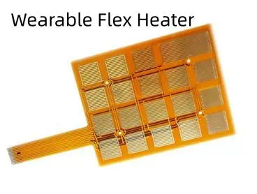
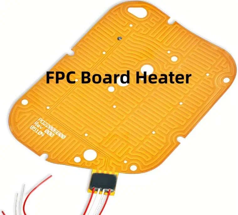
As an engineer and hobbyist, I was looking for a way to create a wearable personal heater that could provide warmth on demand, using my skills in PCB design and electronic circuits. This article details my journey in designing and building a flexible printed circuit board (PCB) heater that can be worn.
Making a wearable heater from a custom PCB provides several advantages:
Thin and lightweight for wearing comfort
Flexible to wrap around different body parts
Customizable shape and size
Precise temperature control
I took inspiration from DIY sous vide immersion heaters and flexible PCB circuits used in wearables. By combining these concepts, I created a battery-powered heated garment perfect for keeping warm during winter outdoor activities.
With these goals and constraints in mind, I could start developing the heater circuit design and PCB layout.
PCB Heater Design
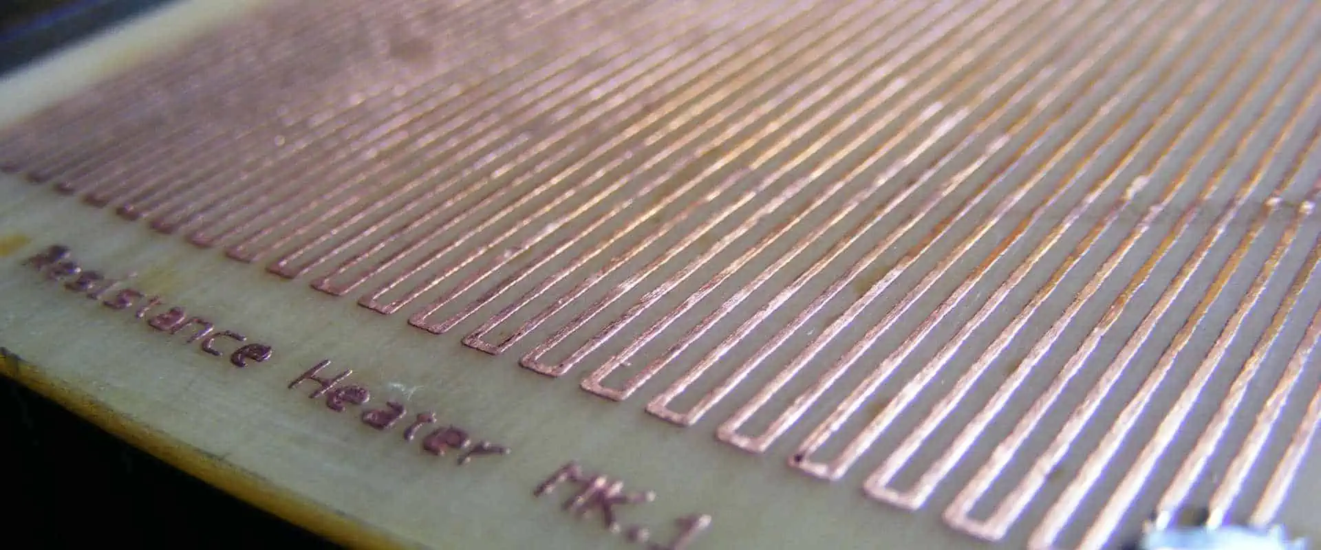
The core mechanism behind the wearable heater is using thin copper traces on a flexible PCB as resistive heating elements. By passing current through the traces, they heat up according to:
Power (Watts) = Current^2 (Amps) x Resistance (Ohms)
To generate the 10 W/sq. inch target power density, I needed the right combination of trace width, thickness, and resistivity.
Heater Traces Layout
I designed a serpentine pattern of traces in two identical zones, allowing dual zone heating control:<table> <tr> <td>
To maximize heat output within the surface area, each zone contains long, winding traces with minimal spacing between them.
5V Boost Converter: Efficiently boosts a USB power bank’s 3.7V input up to 5V output.
Control Unit
Microcontroller Board: I used an Adafruit Feather with ATmega328P MCU and prototyping space.
MOSFET Switches: Use IRF520 high current MOSFETs to switch zone power.
Temperature Sensor: Provides local feedback for closed loop control.
OLED UI: Simple interface using only 3 buttons.
Safety Circuits
Resettable Fuse: Opens if overcurrent draw is detected
Crowbar Circuit: Handles overvoltage from power supply
Watchdog Timer: Auto shutdown if any faults occur in firmware
With dual MOSFETS independently controlling the zones, the microcontroller can maintain precise temperatures by using PID control and PWM. The cutoff fuse and crowbar provide protection from overloads, keeping things safe.
Now to lay out the circuit into a prototype PCB…
Prototyping the Heater PCB
To fabricate the initial heater PCB prototype, I used OSH Park’s flexible circuit board service. This allowed testing the design before investing in an expensive production flexible PCB run.
The empty mid layers act as power distribution planes once I etched openings for connectivity. The thin dielectric foam layers provide insulation between conducting layers.
I iterated through several prototype boards, adjusting the layout as needed to fit components and route traces.
After stuffing both heater zones with components, the final populated prototype looked like:
With the electronics complete, it was time to test out the heating performance…
Center area runs hotter than edges -Difference of ~10°F between hot spot and perimeter
Transient Heat Up Time
Heating from room temperature to 115°F
Reaches 90% temp within 90 seconds
The figures matched well with my initial calculations and simulations for the custom heater traces. After several rounds of testing, I was satisfied with the thermal performance and ready to complete the full heated garment.
Constructing the Heated Garment
With a fully functioning flexible PCB heater, I could assemble it into a comfortable, wearable heated jacket insert by following these steps:
Step 1: Laminate Heater PCB
I coated both sides of the finished heater PCB with a thin layer of silicone conformal coating to provide electrical insulation and water resistance.
Step 2: Cut Fabric Layers
I cut rectangular pieces of fabric to sandwich around the PCB:
Outer fabric shell
Insulating foam layer
Soft inner liner fabric (against skin)
Step 3: Attach Hook and Loop Tape
I added small pieces of Velcro fabric tape to form an adjustable loop around an arm or leg when wrapped.
Step 4: Assemble Layers
I used a sewing machine to assemble all fabric layers together, with the PCB heater sealed inside and contact wires brought out.
Step 5: Attach Wiring and Controller
I connected heater wires to the control PCB board and sealed it inside a small project box for adjusting settings.
And there you have it – a flexible, wearable heater powered by a PCB and controlled by an Arduino!
Once assembled into wearable inserts, I found the flexible PCB heaters performed very well:
Quickly reaches 115°F temp (sustained)
Conforms nicely to shape limb underneath
Thin and lightweight construction
No hotspots detected during use
Battery powers for ~3 hours per charge
However, I noted a few improvement opportunities for future revisions:
Use thicker copper and polyimide layer to increase power density
Improve outer insulation; some water penetration when sweating
Optimize battery selection for longer run times
Add Bluetooth for wireless control
Overall though, given the basic tools and resources I used, I’m thrilled with how my flexible PCB wearable heater came out! It provides the perfect amount of personal heating for helping me stay warm in the winter.
And since the PCB design files are fully shared, you can build your own or even improve on my original design. Just let me know what version 2 of this DIY heated garment looks like!
FAQ
Here are some common questions on building your own PCB-based wearable heater:
Q: What PCB thickness should be used for flexibility?
A: A 4-layer board up to 0.8mm thick works well. The thin dielectric layers enable the entire board to bend and fold easily.
Q: What temperature range can a PCB heater reach?
A: With careful design, you can achieve consistent surface temperatures from 100°F to over 200°F if needed. But higher heat requires thicker copper and better insulation.
Q: Is sealed conformal coating enough insulation for skin contact?
A: For direct skin contact, I recommend laminating fabric insulation layers around the cured PCB for safety and comfort. Silicone coats alone may not provide enough protection long term.
Q: How long can these heaters run on batteries?
A: Battery life depends on heating power needs and battery capacity used. With 5000 mAh USB power banks, I achieved 2 to 4 hours of runtime while drawing around 5-10W total. Adding multiple banks can extend operation further.
Q: What safety concerns exist around DIY PCB heaters?
A: Be sure to properly insulate all traces and high voltage sections. Include fusing, over-temperature monitoring, and redundant physical shutoffs. Never leave powered unattended. Carefully test insulation prior to wearing. Consider low voltage supplies to limit risks.
Conclusion
I had tremendous fun engineering flexible PCBs into wearable heaters for the first time. The circuit design, layout techniques, prototyping iterations, and insulation methods I devised provide a solid starting point for this emerging project area. While DIY electrical garments require great care in safety and testing before regular use, the personalization and customization possible makes it an exciting field ripe for innovation. I welcome you to take inspiration from my heated garment design files and see how you can push wearable PCB tech further with your own creative spin!
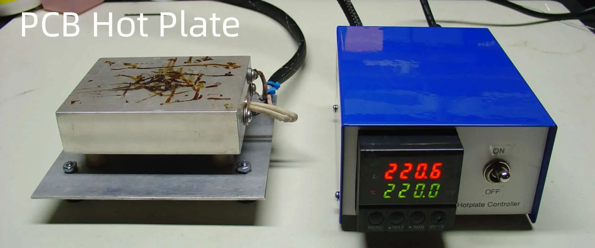
A hot plate comprises an electronically heated platform allowing precision temperature control up to 300°C necessary for print circuit board (PCB) surface mount device (SMD) soldering processes including baking, reflow or rework station preheating. Hot plates assist solder paste curing before component placement as well as post-assembly lead-free solder reflow.
This article details hot plate usage methodologies during PCB SMD population focusing on appropriate SMD sizing, ideal placement locations, optimal heating techniques, process tuning considerations and maintenance best practices when employing programmable hot plate systems to fully leverage their capabilities improving solder joint integrity necessary for reliable electronics functionality across myriad end-use conditions.
Adjustable Stand – Raises hot plate to comfortable height
A sensor feedback loop allows the controller to regulate heating elements embedded underneath the ceramic top achieving exceptionally uniform and stable temperature setpoints within +/- 2°C. Some models even incorporate vacuum holders firmly securing boards during reflow/rework.
Key Hot Plate Specifications
Temperature Range – At least 150°C covers most hand soldering applications
Plate Size – Dimensions suiting largest PCBs needing heating
Control Stability – +/- 2°C for repeatable process consistency
Heating Rate – Up to 10°C/sec facilitates rapid reflow when hand soldering
Vacuum Strength – Prevents thin/warped boards lifting during reflow
Independent Zones – Separate areas preventing localized hotspots
Why PCB Hot Plates Aid Soldering
During hand soldering, applying localized heat only to soldering iron contact points risks temperature gradients across large boards preventing simultaneous reflow when attaching multiple components.
Hot plates provide whole area bottom side heating enabling even preheating facilitating concurrent top side iron solder melting together minimizing deltas preventing cracked joints from board warping arising due to non-uniform thermal expansion.
Precision closed loop thermal regulation also aids solder paste curing, moisture baking or component rework needing consistent heating unattainable using hand-held heat guns. Thereby hot plates simplify achieving process repeatability necessary for quality soldering.
PCB Component Sizing Considerations
Judicious component selection and placement proves vital when hot plate soldering:
Avoid Large Metal-Cased Parts – Significant thermal mass demands more heat input slowing process
Use Low Temperature Solders – Sn42/Bi58 melts faster than lead-free alloys
Place Devices Centrally – Eliminates positioning beyond heated boundaries
Grouping similarly sized SMD parts together also aids batch soldering instead individually processing each element. However balancing these layout considerations against electrical performance needs and routing congestion challenges persists key for complex boards.
Solder Paste Selection
When stenciling paste for hot plate reflow, consider:
Maintaining meticulous soldering logs while methodically varying single parameters during profiling provides the empirical process window necessary for optimizing programmable oven/hot plate routines needed achieving repeatable high-yield results.
Thermal Profile Data Logging
Use thermocouples for logging PCB heating during initial profiling:
Non-Contact InfraRed Thermometers – Rapidly scans board without soldering probes
Type-K Glass-Braid Thermocouples – Rated for over 200°C measurements
Miniature Integrated Probes – Compact formats occupying less space
Multi-Channel Data Loggers – Logs entire oven thermal maps simultaneously
Profiling runs should cover several repeated cycles logging heating/cooling trends for identifying tuning opportunities to meet acceptable process windows.
Such empirical data then supplements oven vendor recommendations for computing optimized thermal routines matching board materials, components, form factors and throughput needs.
Hand Soldering Techniques
When hand soldering complexes boards under hot plates:
Apply Fluxes Judiciously – Use minimal amounts; remixed frequently
Keep Tips Clean – Replace/rewet dirty iron parts hindering heat transfers
While requiring Planning schedule downtime, such actions ensure continuous optimum functionality.
Safety Precautions
Exercise abundant precautions when operating hot plates:
Mandate hand gloves avoiding accidental skin contacts
Confirm boards remain entirely on heated platform
Follow maximum temperature ratings for flammable boards
Cease operations upon seeing smoke possibly indicating scorched flux residues
Allow sufficient cooldown before handling recently energized unit
Such prudence minimizes workplace mishaps or equipment damage risks from operational excursions exceeding safety envelopes across inherently hazardous high-temperature processes.
This guide examined appropriate SMD selection factors, precise paste printing, controlled thermal profiling, data logging aids and safety protocols when employing benchtop hot plates for assisting hands-free bottom preheating delivering rapid yet gentle reflow necessary for reliable lead/lead-free PCB soldering – especially vital producing complex multilayer boards containing moisture sensitive components or high pin count fine pitch devices extremely vulnerable to thermomechanical fractures resulting from uncontrolled heating. Properly incorporating such feedback-controlled programmable platforms significantly enhances assembly repeatability even during low-volume prototype runs using hand soldering. The future potential of additive lateral heat sources for further optimizing board level heating distributions heralds even better soldering yield improvements necessary sustaining further PCB miniaturization trends.
Frequently Asked Questions
What is the advantage of a PCB hot plate over a reflow oven?
Key advantages hot plates offer over large convection ovens include tighter temperature uniformity across small boards via direct contact conduction, closed loop precision hardly achievable using blown heat, smaller form factors suitable for hand assembly stations, lower power saving energy plus faster thermal response attaining quick reflow ideal soldering heat-sensitive components.
What PCB surface finish works best for hot plate soldering?
Exposed PCB surface pad finishes using immersion silver or electrolytic hard gold demonstrate the best solderability for hot plate manual soldering applications given their oxidation resistance at elevated pre-heat temperatures compared to bare copper prone to surface dulling or HASL tin-lead layers tending to melt prematurely ahead of solder pastes preventing intermetallic alloying necessary for sound joints.
Are leaded or lead-free solders preferred for PCB hot plates?
Although leaded solders melt ~30°C lower than lead-free alternatives thereby needing lower peak pre-heat temperatures, given tightening environmental legislation banning lead material usage plus lead-free alloys better resisting tin whiskering risks under temperature cycling necessary for automotive grade boards, lead-free SAC305 or SN100C formulations prove most widely adopted even for hand soldering using benchtop hot plate stations.
How flat must PCB boards be for hot plate soldering?
Ideally, boards should remain completely flat within under 2mm deflection across each linear dimension at peak preheat temperatures to prevent localized solder reflow simultaneously across pads caused by height differentials or air gaps exceeding thermal conduction capabilities of most hot plates having typical 150mm throat depths although advanced versions allow programmatically creating several independent heating zones targeting slightly warped multilayer boards.
How are temperature uniformity verified across PCB hot plates?
Checking hot plate pre-heat platform uniformity involves logging temperature readings using an orthogonal matrix of thermocouples spanning the heated top and then calculating deviation extremes across mapped area for determining necessary modifications either through controller tuning or by physically shimming the heated ceramic element improving flatness thereby attaining under 5°C variance consider acceptable for SMD hot plate soldering applications without causing solder balling issues.
Today’s electronics demand increasingly compact, high-speed PCB designs where every trace and component interaction matters. As operating frequencies routinely reach GHz ranges and signal integrity becomes paramount, simple conductor connections no longer suffice.
Controlled impedance has emerged as a critical factor in PCB performance. Designers must now carefully analyze critical nets, trace geometries, and their board’s material properties to maintain signal quality. In high-speed digital and RF applications, proper impedance management isn’t just beneficial – it’s essential for reliable circuit operation.
Impedance control PCB refers to the process of designing and manufacturing printed circuit boards with specific trace impedances. This technique ensures that the electrical characteristics of PCB traces remain consistent throughout the signal path, which is critical for maintaining signal integrity in high-speed and high-frequency applications.
Why is Impedance Control Important in PCB Design?
Impedance control PCB design is crucial for several reasons:
Signal Integrity: It minimizes signal reflections and distortions, ensuring clean signal transmission.
High-Speed Performance: Essential for devices operating at high frequencies or data rates.
Electromagnetic Compatibility (EMC): Helps reduce electromagnetic interference (EMI) and improve overall system performance.
Compliance: Many industry standards require specific impedance values for certain interfaces.
A trace on the outer layer with a ground plane below. Most common for high-speed signals on outer layers.
Typical Z0: 50ΩEasy to manufactureExposed to environment
Embedded Microstrip
Similar to surface microstrip but with dielectric coating above. Better protection and slightly different impedance characteristics.
Typical Z0: 50ΩBetter protection
Stripline (Symmetric)
Trace sandwiched between two ground planes with equal dielectric thickness. Best EMI shielding and signal integrity.
Typical Z0: 50ΩBest shieldingHigher cost
Edge-Coupled Differential Microstrip
Two parallel traces on outer layer for differential signaling. Used in USB, HDMI, PCIe, and other high-speed interfaces.
Typical Zdiff: 90-100ΩGood noise immunity
Edge-Coupled Differential Stripline
Differential pair between ground planes. Ultimate performance for sensitive high-speed differential signals.
Typical Zdiff: 100ΩBest SI performanceHighest cost
Common Impedance Requirements by Interface
Interface
Type
Impedance
Tolerance
USB 2.0
Differential
90Ω
±10%
USB 3.0/3.1
Differential
90Ω
±10%
HDMI
Differential
100Ω
±10%
PCIe
Differential
85Ω
±15%
SATA
Differential
100Ω
±10%
DDR4
Single-ended
40-60Ω
±10%
Ethernet 10/100
Differential
100Ω
±10%
RF/Microwave
Single-ended
50Ω
±5%
PCB Substrate Materials Comparison
Material
Dk (εr)
Df (Loss)
Tg (°C)
Cost
Best For
FR-4 Standard
4.2-4.8
0.020
130-140
$
General purpose, low-speed
FR-4 High Tg
4.2-4.6
0.018
170-180
$$
Lead-free assembly, automotive
Rogers RO4003C
3.55
0.0027
280+
$$$
RF/Microwave, low loss
Rogers RO4350B
3.48
0.0037
280+
$$$
High frequency, stable Dk
Isola 370HR
3.92
0.025
180
$$
High reliability, server
Megtron 6
3.4
0.002
185
$$$$
High-speed digital, 25G+
PTFE/Teflon
2.1-2.5
0.0009
327
$$$$
mmWave, aerospace
📋 Material Selection Guide
≤1 GHz / General Digital
FR-4 Standard is usually sufficient. Cost-effective for most consumer electronics.
1-10 GHz / High-Speed
Consider low-loss FR-4 or Rogers RO4000 series for better signal integrity.
10-40 GHz / RF Applications
Rogers, Taconic, or similar low-loss materials required for acceptable performance.
>40 GHz / mmWave
PTFE-based materials essential. Consider Dk stability across temperature.
📐
Maintain Consistent Trace Width
Keep impedance-controlled trace widths constant throughout routing. Avoid necking down at component pads if possible, or minimize transition length.
🔌
Reference Plane Continuity
Ensure solid, uninterrupted ground or power plane beneath controlled impedance traces. Avoid routing over splits or gaps in reference planes.
↔️
Differential Pair Spacing
Maintain consistent spacing between differential pairs. Match lengths within 5 mils for most applications. Keep pairs away from other signals by 3x the trace spacing.
📏
Via Considerations
Place ground vias near signal vias for return path. For diff pairs, add ground vias between the pair vias. Consider via stub effects above 5 GHz.
⚠️
Account for Manufacturing Tolerances
Typical impedance tolerance is ±10%. Include this in your design margin. Work with your fabricator to understand their process capabilities.
🧪
Request Test Coupons
Always request TDR test coupons for impedance-controlled boards. Review the test report to verify your design meets specifications before full production.
⚡ Quick Design Rules
✓ Min trace spacing: 3× dielectric height
✓ Diff pair length match: <5 mils
✓ Ground via within 20 mils of signal via
✓ Avoid 90° bends, use 45° or curves
✓ Keep stubs under λ/20 length
✓ Min 3W spacing between traces
💰 Factors Affecting Impedance Control Cost
Controlled impedance typically adds 5-20% to base PCB cost depending on complexity. Understanding these factors helps optimize your design for cost.
1
Tolerance Requirements
±10% is standard. Tighter tolerances (±5%, ±7%) require more process control and testing, increasing cost by 10-30%.
2
Material Selection
Standard FR-4: baseline cost. High-Tg FR-4: +15-25%. Rogers/specialty: +100-400%. Choose based on actual frequency requirements.
3
Layer Count & Stackup
More layers with impedance control = more testing. Asymmetric stackups may require custom lamination, adding cost.
4
Testing Requirements
TDR testing adds cost per board. Coupon testing is more economical for production. Consider testing strategy early.
📊 Relative Cost Estimator
Estimated Cost Multiplier
1.0×
relative to standard non-impedance controlled PCB
💡 Cost Optimization Tips
Use standard ±10% tolerance unless your application truly requires tighter
Consolidate impedance requirements to minimize different controlled structures
Work with fabricator early to optimize stackup for standard materials
Consider coupon testing for production vs. 100% TDR for prototypes
Design for standard prepreg/core thicknesses to avoid custom layups
When discussing impedance control PCB design, it’s important to understand the different types of controlled impedance configurations:
Single-Ended Impedance
Single-ended impedance is the most common type in impedance control PCB design. It refers to the impedance of a single trace measured against a reference plane (usually ground). Typical values for single-ended impedance are 50Ω or 75Ω, depending on the application.
Differential Impedance
Differential impedance involves a pair of traces carrying complementary signals. The impedance is measured between these two traces. Differential pairs are commonly used in high-speed digital interfaces like USB, HDMI, and PCIe. Typical differential impedance values are 100Ω or 120Ω.
Coplanar Impedance
Coplanar impedance refers to traces on the same layer with ground planes on either side. This configuration is often used in RF and microwave circuits. The impedance in coplanar waveguides depends on the trace width, the gap between the trace and adjacent ground planes, and the dielectric properties of the substrate.
Several factors influence the impedance of PCB traces. Understanding these factors is crucial for effective impedance control PCB design:
1. Trace Geometry
The width and thickness of the trace significantly affect its impedance. Wider traces generally have lower impedance, while narrower traces have higher impedance.
2. Dielectric Material
The properties of the dielectric material, particularly its relative permittivity (εr), play a crucial role in determining trace impedance.
3. Stackup Design
The arrangement of layers in the PCB, including the distance between signal layers and reference planes, impacts impedance.
4. Copper Weight
The thickness of the copper used for traces (often referred to as copper weight) affects both the trace’s resistance and its impedance.
5. Surface Finish
Different surface finishes can slightly alter the effective dimensions of the traces, impacting their impedance.
How to Calculate Impedance in PCB Design
Calculating impedance is a critical step in impedance control PCB design. While sophisticated software tools are available for precise calculations, understanding the basic formulas provides valuable insights:
Microstrip Impedance Calculation
For a microstrip (a trace on the outer layer with a ground plane beneath), the impedance can be approximated using:
h is the height of the trace above the ground plane
w is the width of the trace
t is the thickness of the trace
Stripline Impedance Calculation
For a stripline (a trace embedded between two ground planes), the impedance can be approximated using:
Z0 = [60 / √εr] * ln[1.9b / (0.8w + t)]
Where:
b is the distance between the ground planes
Other variables are the same as in the microstrip formula
It’s important to note that these formulas are approximations. For precise impedance control PCB design, especially in high-speed or RF applications, it’s recommended to use specialized PCB design software or consult with PCB manufacturers.
Best Practices for Impedance Control PCB Design
Implementing effective impedance control PCB design requires attention to detail and adherence to best practices:
1. Maintain Consistent Trace Width
Keep trace widths consistent throughout the signal path to maintain uniform impedance.
2. Use Smooth Transitions
Avoid abrupt changes in trace direction. Use curved traces or 45-degree angles for turns.
3. Proper Stackup Design
Design your PCB stackup carefully, ensuring consistent reference planes for controlled impedance traces.
4. Mind the Return Path
Ensure a clear and uninterrupted return path for high-speed signals, typically on an adjacent layer.
5. Differential Pair Routing
For differential pairs, maintain tight coupling and equal length between the two traces.
6. Avoid Impedance Discontinuities
Minimize the use of vias in controlled impedance traces, as they can introduce impedance discontinuities.
7. Use Stitching Vias
When changing layers, use stitching vias near the transition to maintain a consistent return path.
Manufacturing Considerations for Impedance Control PCB
Successful impedance control PCB manufacturing requires close collaboration between designers and manufacturers. Here are key considerations:
1. Material Selection
Choose appropriate PCB materials with consistent dielectric properties for reliable impedance control.
2. Copper Weight
Specify the correct copper weight, as it affects both trace impedance and manufacturability.
3. Tolerances
Understand and specify the required tolerances for trace width and spacing, as well as overall board thickness.
4. Testing and Verification
Implement proper testing procedures, such as Time Domain Reflectometry (TDR), to verify impedance values.
5. Documentation
Provide clear and detailed documentation of impedance requirements to your PCB manufacturer.
Measuring Impedance in Manufactured PCBs
Verifying the impedance of manufactured PCBs is crucial for quality control. Here are common methods for measuring impedance:
1. Time Domain Reflectometry (TDR)
TDR is the most common method for measuring PCB trace impedance. It sends a fast rise-time pulse down the trace and measures reflections caused by impedance discontinuities.
2. Vector Network Analyzer (VNA)
VNAs are powerful tools for measuring impedance, especially useful for RF and microwave circuits. They measure scattering parameters (S-parameters) of the trace, which can be used to calculate impedance.
3. Impedance Coupon Testing
Many PCB manufacturers offer impedance coupon testing as part of their quality control process. Test coupons with controlled impedance traces are included on the panel with the PCBs and measured using TDR or other methods.
Advanced Topics in Impedance Control PCB Design
As you delve deeper into impedance control PCB design, consider these advanced topics:
1. High-Speed Design Considerations
For high-speed designs, factors like skin effect and dielectric loss become increasingly important. These phenomena can affect signal integrity and must be accounted for in impedance calculations and overall PCB design.
2. Impedance Control in Flexible PCBs
Flexible and rigid-flex PCBs present unique challenges for impedance control. The bending of traces and varying dielectric properties in different areas of the board require special consideration.
3. Electromagnetic Simulation
Advanced electromagnetic simulation tools can provide detailed insights into signal behavior and impedance characteristics, allowing for more precise impedance control PCB design.
4. Embedded Passives and Impedance Control
The use of embedded passive components can impact impedance control. Understanding how to design and manufacture PCBs with embedded passives while maintaining controlled impedance is an advanced skill.
Troubleshooting Common Impedance Control PCB Issues
Even with careful design and manufacturing, impedance control PCB issues can arise. Here are some common problems and their solutions:
1. Impedance Mismatch
Symptom: Signal reflections and degraded signal quality. Solution: Verify trace widths, dielectric thicknesses, and material properties. Adjust design or manufacturing process as needed.
2. Crosstalk
Symptom: Interference between adjacent traces. Solution: Increase spacing between traces, use guard traces, or adjust layer stackup to improve isolation.
3. Inconsistent Impedance Along Trace Length
Symptom: Varying signal quality at different points along the trace. Solution: Ensure consistent trace width and reference plane integrity throughout the signal path.
4. Resonance Issues
Symptom: Signal integrity problems at specific frequencies. Solution: Analyze and adjust trace lengths to avoid creating unintentional resonant structures.
Future Trends in Impedance Control PCB Design
As technology continues to advance, impedance control PCB design is evolving to meet new challenges:
1. Higher Frequencies
With the advent of 5G and beyond, PCB designs must accommodate ever-higher frequencies, requiring more precise impedance control.
2. Miniaturization
As devices become smaller, maintaining controlled impedance in dense, compact layouts becomes more challenging.
3. New Materials
Development of new PCB materials with improved dielectric properties will offer new possibilities for impedance control in high-performance applications.
4. Artificial Intelligence in PCB Design
AI-assisted design tools are emerging, potentially revolutionizing how we approach impedance control PCB design and optimization.
Conclusion
Mastering impedance control PCB design is essential for creating high-performance electronic products in today’s fast-paced technological landscape. From understanding the basic principles to implementing advanced techniques, this guide has covered the critical aspects of controlled impedance in PCB design and manufacturing.
Remember, successful impedance control PCB design is not just about following rules and formulas. It requires a deep understanding of electromagnetic principles, close collaboration between designers and manufacturers, and a commitment to continuous learning and improvement.
As you apply these principles in your PCB projects, you’ll develop an intuition for impedance control that goes beyond mere calculations, leading to more robust and reliable electronic products. Whether you’re designing high-speed digital circuits, sensitive analog systems, or cutting-edge RF applications, mastering impedance control PCB design is an essential skill that will set your work apart in the ever-evolving field of electronics.