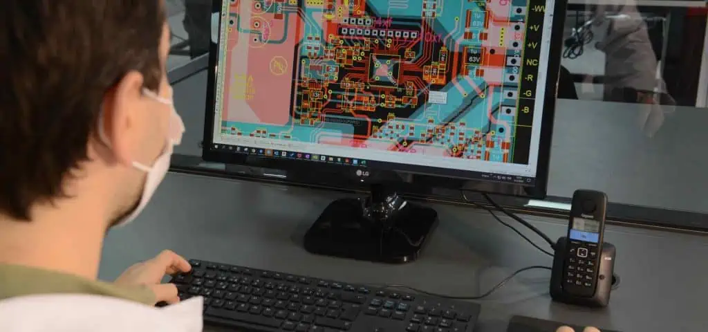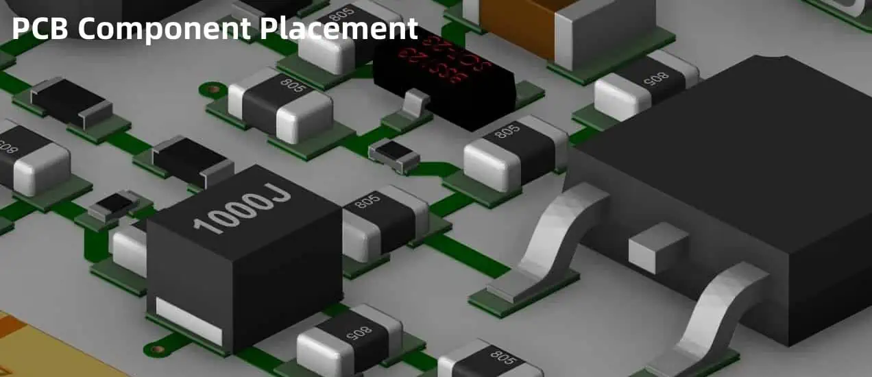
Printed circuit board (PCB) component placement refers to the layout and positioning of the various parts that will be soldered onto the PCB surface. Following optimal engineering guidelines during the design stage facilitates PCB assembly and performance. Methodical component orientation enhances reliability, testability, and manufacturability while minimizing interference.
This article explores essential PCB component placement recommendations through topics like:
Grouping Functional Blocks
PCB functionality often involves both analog and digital circuits along with supporting elements like power systems. Grouping related components and traces into functional blocks or zones aids design and troubleshooting:
Digital Logic Sections
- Place microcontrollers and peripherals together with associated discrete logic
- Cluster high-speed bus lines to restrain lengths
- Distribute bulk capacitance evenly across logic for current demands
- Arrange clock distribution topology to minimize skew
Analog Signal Chains
- Group sensors, amplifiers, filters, converters in sequential chains
- Place noise-sensitive components nearby for short protected traces
- Allocate room for large value precision passives
- Enable easy test point access to verify operation
Power Supply Modules
- Combine input protection, filtering, regulation in coherent formations
- Locate bulk storage capacitors near consuming ICs
- Enable thermal design for expected power dissipation
- Facilitate supply isolation, sequencing, and monitoring as needed
Such functional groupings with spatial affinity expedite routing and debugging during design revisions while supporting assembly.
Component Orientation

Parts on circuit boards can face different directions during placement. Their orientation should balance various tradeoffs:
Readability
Components should be readable from a keepout zone edge without requiring board flipping. This aids manufacturing and field troubleshooting. Exceptions can be made for RF blocks.
Pin Accessibility
Enable soldering or clipping onto terminals without obstruction from other devices or chassis structures.
Thermal Transfer
Position hot elements like transistors to connect directly to sinks with thermal pads or leads.
EMI Control
Align components to utilize inherent electromagnetic shielding from packages and chassis features.
Routing Friendliness
Choose orientations allowing straightforward trace paths to desired pin linkages without convoluted wiring around packages.
By considering multiple aspects, components can achieve better configured installation. Engineers may designate some priority orientations for critical elements while allowing assembly flexibility for generic parts.
Component Grouping Categories
In addition to functional clustering, parts often get allocated into zones per these categories:
| Category | Description |
|---|---|
| Critical | High precision analog or custom circuits |
| Semi-critical | More forgiving analog, fast digital |
| Non-critical | Industrial grade analog, medium-speed logic |
| Generic | Commercial grade parts |
Higher performance sections deserve greater layout care and protection while more lenient specifications enable placement flexibility if interference avoided.
Components get assigned grouping priorities based on factors like:
- Needed measurement or timing precision
- Signal integrity requirements
- Anticipated heat dissipation
- Frequency of adjustments/replacements
- Known reliability statistics
- Radiation or noise sensitivity
Board sections then reflect appropriate rigor. Production processes likewise adapt to give proper component handling and inspection care by grouping.
Placement Rules of Thumb
General component placement guidelines that aid manufacturability include:
Consistent Alignment
Keep uniform orientation and spacing between identical adjacent components for easier assembly and inspection. Exceptions can be made for thermal reasons.
Accessible Identifiers
Enable visible markings on parts including polarity indicators without obstruction for production verification.
Edge Clearance
Allow sufficient space between components and PCB edges for machining tolerances without clipping.
Probe Clearance
Do not place parts that could block debug test probe access beside critical test points or programming headers.
Reflow Shadowing
Avoid tall components shadowing shorter elements and preventing even heating during solder reflow ovens.
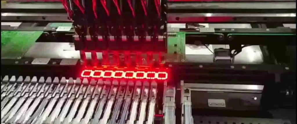
Pick and Place Suitability
Ensure adequate room around each component for vacuum nozzle or mechanical gripper acquisition without colliderisk with adjacent parts.
Adhering to fundamental placement practicalities that consider eventual fabrication and diagnostics saves much iteration.
Layer Separation Disciplines

PCBs intermix surface mount and through-hole technologies across layers. Some separation strategies avoid problems:
Segregate Power Planes
Assign entire board layers just for voltage distributions to minimize splits and maximize current capacity.
Dedicate Ground Planes
Provide solid lower impedance reference planes for return currents rather than mixing grounds with signals.
Component Layer Pairing
Place associated tiny surface mount parts on the sides of the PCB adjacent to their connecting component leads to simplify routing without additional layers.
Escape Via Proximity
Start drill holes carrying signals between layers close to the originating component pads to limit stub lengths.
Contact Clearance
Ensure adequate insulation between traces linked to distinct potentials on any given layer based on voltage.
While dense efficient PCB stacking remains vital in miniaturized products, following basic practices prevents unintended interactions.
Design for Manufacturing
Considering assembly workflows during layout facilitates production and minimizes errors:
| Concern | Guideline |
|---|---|
| Pick and Place | Enable component grasping from at least one direction without collisions |
| Solderability | Place similar terminal types together per process limitations |
| Inspectability | Allocate room for visual access to both board sides |
| Test Access | Include measurement testpoints at key nodes |
| Reworkability | Space replaceable items with room for tools |
Accomodating fabrication constraints up front prevents extensive layout reiterations that stall development.
Design for Testability

Validation access allows fault tracing:
| Method | Provisions |
|---|---|
| Voltage Taps | Expose power rails for metering |
| Test Points | Break out hidden signals to measure |
| JTAG Circuitry | Connect IEEE 1149.1 test bus |
| Bed of Nails | Grid array piercing for in-circuit checks |
| Emissions | Ensure chassis tapping visibility |
While attainment of functionality remains foremost, failure diagnosis requires preparatory features.
Design for Reliability
Many factors influence component survival:
| Driver | Approach |
|---|---|
| Thermals | Enable heat transfer from hot elements |
| Vibration | Anchor mechanically vulnerable components |
| Contamination | Apply conformal coatings in dirty environments |
| Moisture | Minimize absorbed moisture with sealants |
| Fatigue | Avoid materials with mass mismatches inducing cracks |
Avoiding or mitigating known stressors improves durability.
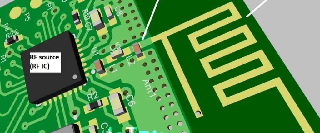
Design for EMI Control
Careful layout facilitates emissions and susceptibility management:
| Objective | Tactic |
|---|---|
| Noise Isolation | Distance sensitive analog away from dirty digital |
| Return Current Control | Localized decoupling near active devices |
| Interface Filtering | Ferrites beads and caps at external I/O |
| Internal Shielding | Routing separation gaps between critical signals |
| Signal Symmetry | Match line lengths and proximal reference returns |
Controlling path geometry and energy flow minimizes interference potential.
Design for Signal Integrity
Track layout impacts pulse fidelity:
| Issue | Mitigation |
|---|---|
| Reflections | Controlled impedance lines |
| Ringing | Termination resistors near receivers |
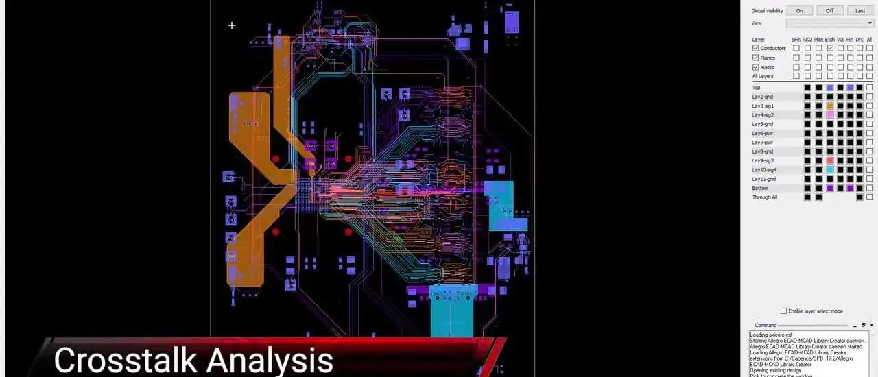
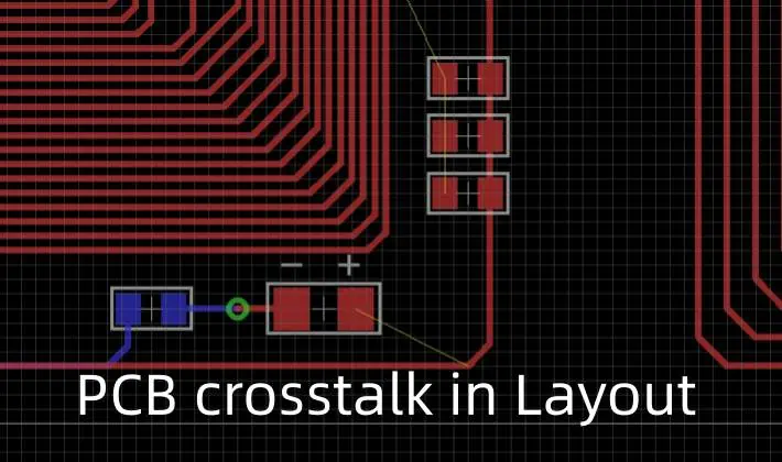
| Crosstalk | Ground and power plane isolation barriers |
| Radiation | Minimize trace resonance and loop areas |
Simulations assess margin from grainular propagateeffects.
Software Placement Tools
Modern electronic computer aided design (ECAD) environments provide sophisticated assistance for intelligent component arrangements via:
Cost Functions
Multi-parameter quantified heuristics rating alternative locations based on weighted priorities.
Constraint Systems
Hierarchies of conditional rules and spacing requirements between components or features.
Optimization Algorithms
Iterative evaluation cycles gradually improving aggregate metrics like timing paths or wireability.
Machine Learning
Training prediction models on empirical data to suggest placements suited for routing.
Such automation leverages extensive context awareness and computation bandwidth to highly improve resulting layout quality. But human supervision remains essential for specification nuances.
Specific Component Types

Special placement considerations apply for certain particular device classes:
Sensors
Minimize conductive or radiative noise injection into susceptible analog front ends through distance and orientation. Local filtering helps too.
Oscillators
Prevent interference or leakage from clock sources corrupting slow precision analog signals. Strategic spacing and grounding prevents false triggers.
Memory
Series terminate high speed data lanes. Control impedance discontinuities from branching data bus topology.
Microcontrollers
Facilitate debugging and programming access with test points or headers. Aid thermal dissipation.
Voltage Regulators
Position bulk capacitors adjacent to each supply pin to absorb transient switching currents.
Optoelectronics
Guide directional element wiring for installation alignment including isolation barriers.
Transformers
Maximize mutual inductive coupling with short straight segment spacing while preventing flux leakage into other components. Control resonant ringing.
Crystals
Keep ultra short traces between oscillators. Prevent amplitude loss with proper load capacitance. Block noise infiltration.
Accommodating context specific needs during broader organization keeps functionality optimal.
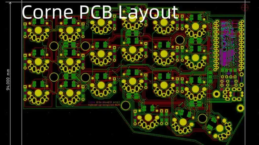
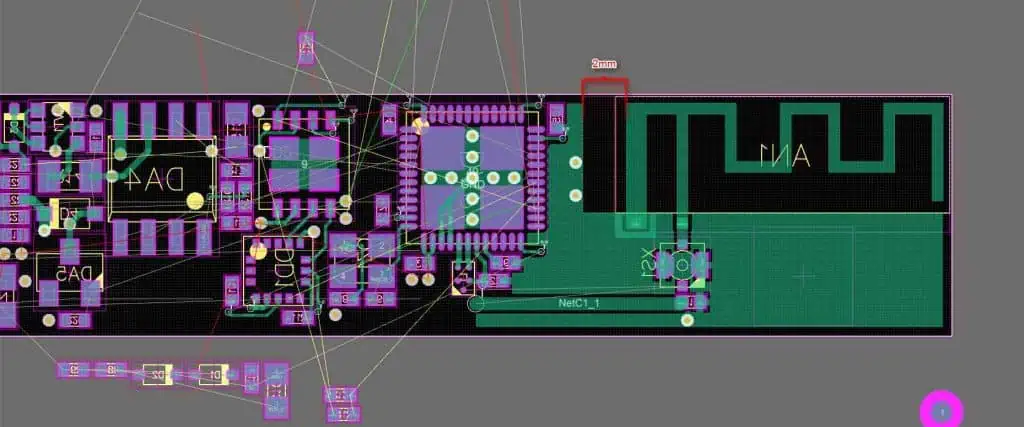
Component Placement Example
Here is an example PCB layout following structured placement conventions with annotations:
Grouped functional regions separate noisy digital logic, analog measurement channels, microcontroller supervision, and power supply conditioning. Components align consistently for manufacturability. Critical paths remain short with testability access.
Careful zoning meets operational needs while easing production and diagnosis. Extensive labeling matches schematics for clarity across documentation. Such disciplined organization professionals to understand, assemble, and maintain complex boards ultimately enabling functioning products.
Frequently Asked Questions about PCB Component Placement
Here are some common questions around PCB component placement guidelines:
What are the most important PCB placement considerations?
The key PCB placement guidelines are:
- Group related functional blocks together
- Orient components for balance thermals, access, emissions
- Impose consistency rules aiding manufacturing
- Control layer types for crosstalk risks
- Design for assembly processes and testability
- Mitigate stresses hurting reliability
How does software assist optimal PCB layout?
Advanced ECAD software provides:
- Cost functions rating alternative sites
- Rule constraint systems
- Iterative optimization algorithms
- Machine learning placement models
This automation aids human diligence.
What separate concerns should group into difference PCB areas?
Typical separated PCB regions encompass:
- High speed digital logic
- Precision low level analog sensing
- Noise sensitive radio circuits
- High power output buffers
- Switch mode power supplies
Separation contains interference.
Where should the most timing critical PCB components get placed?
The highest speed components should locate:
- Near processors and control logic
- With shortest trace runs to memory
- Maximum distance from supply noise
- On inner layers for shortest lines
This minimizes propagation latency.
How can PCB reliability be improved through placement?
Reliability oriented placement involves:
- Heat spreading from hot elements
- Vibration isolation mounts
- Conformal coatings in harsh environments
- Moisture control barriers
- Fatigue prevention supports
Taking materials science into account aids durability.
Careful PCB component placement directly enables operational success and quality over product lifetimes. Prioritizing key circuit needs while respecting manufacturability results in electronics that deliver value.