How to Add Multiple PCBs in one KiCad Project

KiCad EDA suite is a powerful open-source electronics design automation platform enabling professionals and hobbyists alike to take electronic systems from concept to final routed PCB layout.

A major advantage of using KiCad over some commercial EDA tools is it allows including multiple PCB configurations within the same project design.

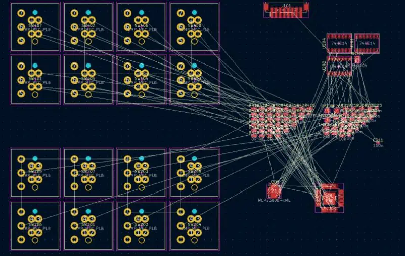
This is beneficial when dealing with complex designs requiring several inter-dependent circuit boards or versions to fully implement the target electronics hardware end-product.

This article provides a step-by-step walkthrough on how to correctly structure and manage multi-board KiCad projects, leveraging inheritance relationships to maximize design reuse. Screenshots demonstrate the key steps involved.

Follow along to learn how to efficiently architect complex multi-PCB solutions as one Master Project in KiCad.

Multi-Board Project Scenarios

Some typical use cases where designing several PCBs as part of consolidated project in KiCad makes sense:

  • Main Board + Daughter Boards – Eg. CPU board + display board combinations with interconnection through high density connectors
  • Board Sets – Devices involving panels/racks with duplicate PCBs plugged into backplane bus structure
  • Versions/Derivatives – Spinning off variants like HW version 1.0, 1.1, 1.2 of base design
  • Master/Slave System – One primary controller PCB with additional peripheral PCBs

In above cases, instead of managing each PCB layout completely independently in isolated KiCad projects, you can define linkage and inheritance relationships between boards early on during the design phase. This allows propagation of changes across dependent boards later avoiding painful rework.

Let’s see how step-by-step.

Configuring Multi-Board Project Structure

The first step is to configure the project structure to accommodate multiple boards belonging to same overall system design. This sets you up to achieve maximum re-use and consistency across individual PCBs due to centralized configuration inheritance reducing duplication or variation by error through project life cycle.

Start Fresh New Project

Launch KiCad and select File > New Project > New Project

Pick any folder location to host the Master Project. This will hold all the individual PCBs and common data.

Create “Project Level” Schematic Folder

Click Add Existing Folder to Current Project toolbar button showing green icon with “plus” symbol.

Browse to folder projectname just created and select subfolder path:

Copy code

projectname/-schematics

This establishes main /-schematics folder for holding any common schematic documents used across ALL boards like power or interface definitions.

Generate Each Board#X Schematic Sheet

Still under the Common Schematic Folder path in left tree view, now create respective schematic document for EACH planned PCB layout board.

Right click mouse, select Create New Schematic

Do this sequentially to initialize first sheet schematic file individually for however many boards intended in full project scope.

Eg. For 4 PCBs:

  • board1.sch
  • board2.sch
  • board3.sch
  • board4.sch

schematic sheets now created ready for circuit drawing later for each planned board.

Next Complete PCBnew Configurations

Repeat the same process now instead under the main project root to initialize corresponding .kicad_pcb layout file for each board schematic created already

Eg. For 4 PCBs:

  • board1.kicad_pcb
  • board2.kicad_pcb
  • board3.kicad_pcb
  • board4.kicad_pcb

These .kicad_pcb files inside root will become respective PCB layout containers related to each schematic sheet after netlist import.

This table summarizes the multi-board project folder structure and file types configured:

LocationFile TypeDescription
/project/schematics.schCommon Schematic Sheets
/project/.kicad_pcbIndividual PCB Layout

We now have framework ready to start actual PCB design work!

PCB Circuit Schematic Design Stage

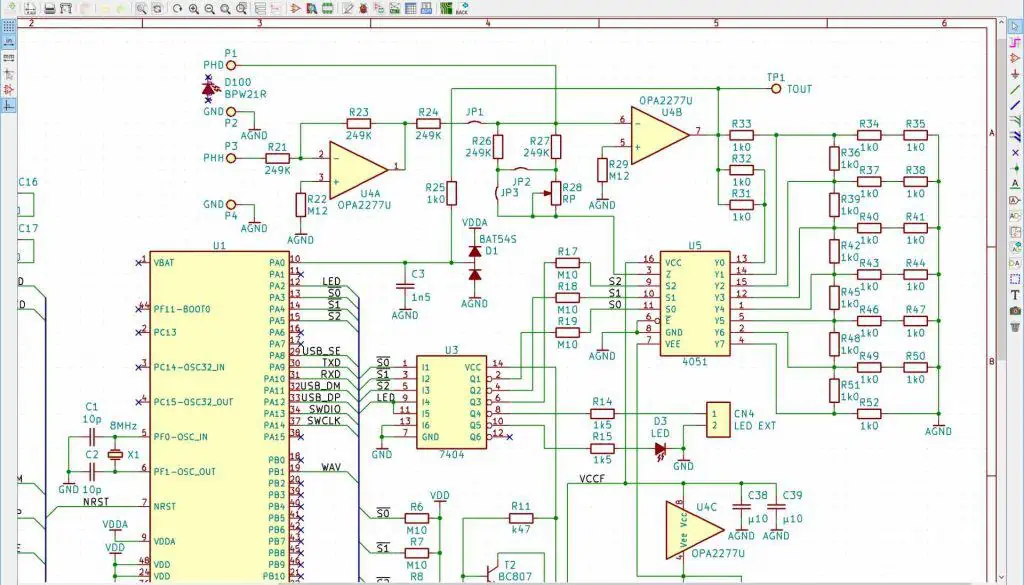
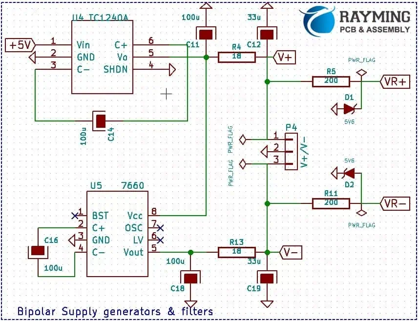
With blank schematic sheets created ready per board, we can begin capturing actual circuits and connectivity. Standard workflow applies just like single board project.

It helps conceptually dividing schematics as:

  • Common Circuits – Schematics logic used by multiple boards eg. power input filtering section
  • Base Circuits – Baseline schematics sections reused by derivative boards via inheritance
  • Unique Circuits – Schematics logic only applying to that specific board

This distinction helps manage change control between shared versus child schematic sheets when alterations occur later down the development timeline.

Follow standard schematic capture best practices as well creating logical schematic architecture for each PCB through combination of:

  • Part symbols from installed component libraries
  • Bus lines to reduce complexity
  • Hierarchical structure using sub-sheets to simplify
  • Net and wire labeling
  • Design rule checks to validate integrity of connections

Cross Probe Between Schematics

Use the KiCad Cross-probing toolbar icon showing magnifying glass symbol to quickly navigate across sheets to trace wires connections between schematics as complexity builds up.

Output Schematic Netlists

Upon finishing respective board’s schematic sheets design work, next output netlist connectivity file. Repeat this process individually for each board’s schematics.

Steps:

  1. Open respective .sch schematic sheet
  2. Tools > Generate Netlist > PCBNew Netlist
  3. Save netlist as eg. board1.net for each board
  4. Repeat generating one netlist per board in project

Netlists act as bridge linking logical schematic connectivity to physical PCB layout.

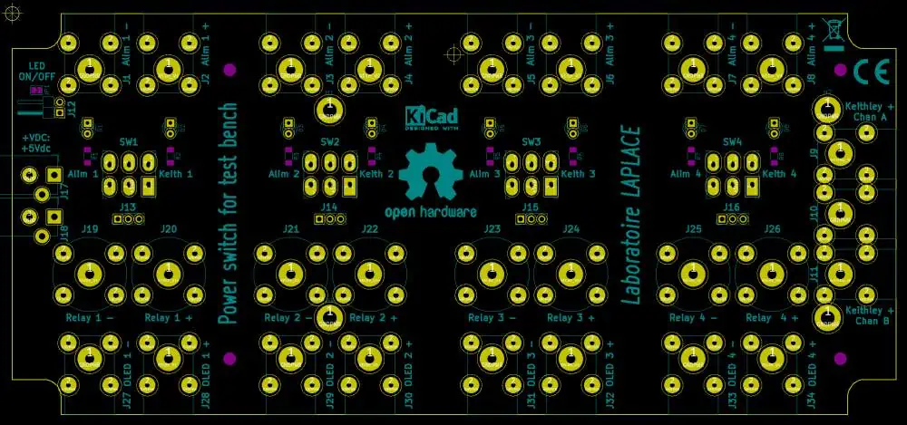
PCB Layout Routing Stage

With connectivity netlists files now available board-wise, we can focus attention to converting schematics into routed PCB.

Again standard workflow applies – initialize board sizes, import netlist, assign footprints, run ERC, place components, route traces until completion for EACH board independently.

However, some additional considerations working on complex multi-board projects include:

Cross Probing Between Layouts

Use the same Cross-Probe toolbar button to quickly navigate between layouts by clicking pushpin marker to understand connectivity spanning across boards.

Inheritance Concept

Leverage inheritance relationships early instead of duplicating similar circuits or networks again. Eg. Common power supply section from one layout can propagate to other boards via cross-probing rather than redrawing.

Validate Across Boards

Before finalizing layouts, cross-validate that schemes used for connectors, mounting holes, silkscreen artworks are consistent across boards which will eventually interface during system assembly stage downstream.

Final Manufacturing Output Handoff

Upon completing all PCB layouts routing and checks, last step is generating manufacturing CAM outputs – Gerbers, NC Drills, Assembly drawings etc. – needed to fabricate the bare boards with a PCB supplier.

Again same process done earlier for single board projects applies here.

Some pointers when submitting manufacturing gerber data for quotation:

  • Send separate zip folders per PCB for clarity even though single project
  • Use consistent file naming conventions indicating parent project
  • Include precise bare board fabrication and solder masking requirements
  • Provide accurate target quantities needed for each board reflecting overall system build volumes

This completes end-to-end design process to realize complex electronics systems made up of multiple PCBs configurations managed efficiently as one Master Project in KiCad EDA tool.

FAQs

What is the best folder structure for multi-board KiCad project?

Below folder architecture allows clean separation between common and board-specific logical assets when dealing with multi-PCB project:

/-projectname

  • /schematics (common schematic sheets)
    • power.sch
    • busdef.sch
  • /board1
    • board1_schematic.sch
    • board1.kicad_pcb
  • /board2
    • board2_schematic.sch
    • board2.kicad_pcb

So keep shared documents in parent level folders while individual PCB data under respective child folder.

How do I check differences between PCB layouts in multi-board project?

When iterating on designs with multiple boards, it helps cross-validate differences between board Layout versions.

KiCad provides built-in layout comparative functionality:

  1. Open first board layout .kicad_pcb
  2. Select menu Tools > Compare PCB Layouts
  3. Browse and select second .kicad_pcb layout design
  4. Adjust ignore thresholds if needed under various comparison criteria

This does smart diff analysis reporting differences between layouts helping synchronize changes across dependent boards.

Can I split complex schematic across multiple sheets for cleanliness?

Yes, when working with multi-page schematics for big designs, instead of cramping up all logic into giant single sheet canvas, apply divide and conquer approach:

  • Break down by functional modules
  • Use hierarchical sheets and ports
  • Cross link between sheets using invisible nets
  • Show external connectivity through block symbols

This reduces scrolling needs and aids readability helping focus on specific logic section when making edits instead of getting overwhelmed viewing entire schematic complexity on one page.

Cross-probing facilitates navigation while ERC checks validate connections consistency between fragmented schematic sheets. Page index table helps map document structure when interfacing design reviews. So fully utilize tools at disposal to creatively architect complex schematics refinement modularly across multiple sheets using KiCad’s versatile EDA environment capabilities.

I hope this gives a good starting point for electronics designers to efficiently structure KiCad projects involving multiple PCB layouts instead of struggling managing disconnected documents. Follow the principled approach touching on configuration, re-use via inheritance, cross-validation between boards and version control to yield productivity benefits when dealing with high complexity multi-board system solutions as one Master Project.

How do I convert a Schematic to PCB Layout in KiCad (Step By Step)

KiCad is a free, open source electronics design automation suite for Windows, Mac, and Linux, widely used by hobbyists, makers, and engineers to design printed circuit boards (PCBs).

Converting your KiCad schematic to PCB layout is an essential step in the process of designing a custom PCB, allowing you to define the physical board and component layout matching your circuit schematic connectivity.

This article provides a step-by-step workflow to successfully move from schematic capture to populated PCB layout using KiCad version 5.1.9’s schematic and PCB editor tools. Screenshots illustrate the key steps.

Let’s get started!

YouTube video

KiCad Design Flow Basics

Below are the basic work stages as you move from concept to finished PCB manufacturing file output when using the KiCad EDA tool suite:

  1. Schematic Capture – Draw circuit diagram connecting components with nets
  2. Schematic Symbols Creation – Make new parts with unique symbols and footprints
  3. Schematic Annotations – Assign reference designators to parts
  4. Netlist Generation – Output connectivity netlist file (.net)
  5. Footprint Assignment – Associate footprints to schematic parts
  6. Design Rule Check – Validate schematic for ERC/DRC errors
  7. PCB Layout – Convert netlist to board with parts placed and routed
  8. Gerber File Generation – Manufacturing output from PCB

We will focus specifically on steps 4 to 7 which enable progression from completed schematic diagram to functional PCB layout, ready for fabrication.

Generate Netlist File From Schematic

Schematic Design in KiCAD

Once your schematic circuit drawing in the KiCad Eeschema schematic editor is logically complete with part symbols wired by nets representing connectivity just like the circuit should operate in physical reality, we are ready to move from schematic to board layout.

The NETLIST file acts as the bridge between the schematic sheet components connectivity and the layout board definition.

To generate a netlist:

  1. Select menu Tools > Generate Netlist Files
  2. Select the checkbox for format Pcbnew (*.net)
  3. Enter filename test_board for the netlist
  4. Select checkbox option Generate single net for unconnected pins
  5. Click OK button

This will generate test_board.net file with net connectivity data matching your schematic diagram’s circuit logic.

The key output netlist formats from Eeschema used at different points in the PCB design process are:

Netlist FormatDescription
.netPCBNew format used for PCB layout routing
.xmlPCBNew format used to import custom schematic footprints
.bomBill of Materials format for assembly

For now, we need the .net PCBNew netlist file that has extracted nets and component connectivity intelligence from the schematic.

Time to move to the PCB Layout editor.

Import Netlist into PCBNew Layout Tool

The PCB Layout editor tool within KiCad is named Pcbnew. This is the canvas where we will map our schematic circuit’s logical connectivity defined graphically in Eeschema down onto the physical domain of the PCB board that will be manufactured.

To import the generated netlist file:

  1. Launch Pcbnew from the KiCad toolbar
  2. Go to menu File > Import Netlist
  3. A dialog prompts you to select the *.net netlist file previously created.
  4. Select the checkbox option Keep Existing Libraries
  5. Click OK

This will open up the main PCB layout canvas and import all the parts and nets defined in our source schematic, ready for board layout work.

Run Electrical Rules Check

Before rushing into board layout placement and routing, it is good practice to run an electrical rules check on the imported netlist to spot any violations with component pin mappings or missing connections compared to the schematic.

Go to top toolbar Tools > Electrical Rules Check

KiCad will analyze the entire netlist and schematic connectivity, flagging warnings if finds any:

  • Unresolved component pin numbers conflicts when mapping schematic symbols to PCB footprints
  • Missing connections / continuity issues versus the schematic sheet
  • Duplicate reference designators assigned
  • Etc.

Address any errors or warnings reported at this stage before further progressing the design conversion. Once ERC passes cleanly, we can be confident to continue with component placement and layout work confident that the PCB connectivity matches the schematic completely.

Assign PCB Footprints to Components

Setting Footprints
Setting Footprints

Every schematic symbol needs a matching PCB footprint assigned, which defines the physical land pattern on the board matching how component terminals will eventually solder down.

To assign footprints:

  1. With PCB board open, select menu Tools > Assign Footprints
  2. A spreadsheet loads with list of all schematic parts.
  3. Choose matching PCB footprint required from libraries already installed for each part.
  4. Saved selections automatically get mapped.

Repeat for all components ensuring every part has both:

  • Unique schematic symbol in schematic editor
  • Corresponding PCB footprint in Pcbnew layout tool

This cross-mapping connects the gates and pins of abstract schematic symbols to real solderable terminations on board.

PCB Layout Design Setup

Before placement and routing, some initial PCB layout design rule and workspace configurations need defining first:

  • Board outline dimensions
  • Copper layer counts
  • Grid & Component clearance rules
  • Net classes for trace widths/clearances
  • Routing zones definition
  • Layer stack table

Tools under Design Rules and Preferences menus allow correctly pre-setting these parameters matching circuit needs and capabilities of your PCB fabrication process.

For a simple single-sided PCB:

  • Define rectangular board dimensions under Page Settings
  • Add Keepout layer graphical boundary showing max size
  • Set 50mil grid spacing under Preferences
  • Define clearance rules between tracks, pads, vias
  • Map layers to physical PCB fabrication layers

Default settings tables can be used initially and refined later once placement is underway.

Begin Component Placement

We can now start intelligently placing components on the PCB canvas to gradually transform from rats nest to routed board layout matching schematic.

Steps for component placement:

  1. Select component to place from list of imported parts from schematic
  2. Move crosshair cursor to desired location on board
  3. Click or tap to anchor component at chosen position.
  4. Orient part footprint by R key rotation if needed
  5. Repeat placing all parts onto board canvas

Tips for good placement practices:

  • Follow logical grouping – Eg. place together related resistors, caps, ICs etc.
  • Start placing parts from a fixed reference like one board corner
  • Place parts from large to small size
  • Watch spacing – provide room for traces between parts
  • Think ahead for track routing paths
  • Place parts on front layer first then back layer

There are no fixed placement rules – experiment until parts layout passes visual sanity check ensuring adequate spacing while following natural circuit zones matching schematic flow.

Use grid snap and zoom controls to fine tune component locations as you work through placing the imported parts list.

Interactive Routing of Component Connections

F-Component Routing Techniques

Having all parts dropped means we now need to connect the dots – to make tracks linking parts pins together as electrically defined by our netlist connectivity imported from the schematic. This is the routing stage.

To interactively route:

  1. Select signal layer intended for trace
  2. Choose routing tool – track/via/wire
  3. Click trace start point – say a component pad
  4. Route trace and click destination pad
  5. Repeat tracing all points in same signal net

Routing Tips

  • Minimize via counts on signal layers
  • Use angled traces instead of meanders
  • Complete power traces first then signals
  • Route one trace end to end before starting next trace
  • Think neatness – avoid chaotic board appearance.

Use grid and snap controls to tidy up traces. Switch layers when changing routing direction avoiding collisions. Toggle rats nest view to verify unrouted connections pending.

The goal is to effectively link component pads together using copper track traces layer by layer until the rats nest fully disappears.

Your routed board should perfectly mirror the schematic connectivity down to the physical domain once routing is complete.

Final Checks – DRC, 3D View, Emulate

Before generating manufacturing gerber and drill files, run final checks:

  1. Design Rule Check – Validate no clearance violations under menu Tools > Design Rule Check
  2. 3D View – Under View > 3D Viewer visually check for missed connections in 3D mode
  3. Emulate – Tool Tools > Generate Footprint Positions File exports a .pos 3D assembly file from the board to mechanically trial component fit, clearances etc. in a New Project

Fix any last minute minor issues based on the feedback from these validation checks.

Output Gerber and Drill Files

Finally, we are ready to produce manufacturing outputs by plotting gerber masks and drill hits database.

Steps:

  1. Menu File > Fabrication Outputs.
  2. Select All layers you want outputs for- Top copper, bottom copper etc.
  3. Ensure options to generate Drill Map (.drl) file is selected.
  4. Click Make Plots button to save gerber files.

Send the Gerber zip file bundle with .drl drill map to your PCB fabrication vendor’s order upload portal or rep to get your designed bare boards manufactured now!

Final Words

kicad-schematic

And that concludes converting a KiCad schematic drawing down to functional PCB layout ready for fabrication and assembly.

The key concepts covered again:

  • Generate netlist connectivity file from schematic capture
  • Import this into new PCBnew layout project
  • Assign footprints matching schematic symbols
  • Follow methodical placement and routing workflow
  • Complete design rule checks before output
  • Export manufacturing plot gerber and drill data

As you gain proficiency translating schematic circuits to routed boards using the KiCad open source EDA tool suite, your custom PCB realization confidence and speed only gets better through applying these fundamentals incrementally to build experience.

Hope this gives electronics hobbyists, makers and engineers a helpful starter framework to take first concept schematics through to manufacturable layout output systematically using the popular KiCad platform.

Good luck with your next schematic to PCB layout project!

FAQs

What are some key hotkeys useful for PCB Layout in KiCad?

General Navigation

  • mm – Move origin crosshair
  • Jump – Rapidly move canvas to selected object
  • < > – Flip Board
  • a – Select layer/tool/settings
  • z – Dynamic zoom
  • g – Toggle grid visibility

Layers & Colors

  • l – Flip current layer
  • Shift+S – Stack colors
  • ./, – Next/previous layer

Editing Actions

  • m – Move footprint
  • r – Rotate footprint
  • f – Flip footprint
  • Del – Delete item

Trace Routing

  • x – Route track segment
  • v – Place via
  • Shift – Cycle through available widths
  • . , – Cycles displayed nets

Consult full KiCad PCB hotkeys list for all shortcuts available.

What’s a good work flow for routing a complex board in KiCad?

For a complex board with high component density and tight clearance requirements, here is an efficient professional routing workflow to follow:

1) Have power input section already defined
2) Place any shield can components first establishing space
3) Grid place groups of same-function parts (ICs, caps etc)
4) Route power buses first on inner layers first
5) Fanout traces from each group keeping same nets together
6) Complete high-speed traces first, minimize vias 7) Use grid to tidy up traces layout iteration by iteration
8) Do most routing on outer layers keeping inner organized
9) Treat every trace uniquely, don’t batch all connects
10) Continually DRC check; validate 3D view for sound assembly

Following the above methodical placement-routing sequence minimizes chaos, rework and ensures optimal board layout quality from complexity perspective.

How do I calculate trace widths in KiCad to handle required current loads?

You can either manually calculate appropriate copper trace widths on PCB to safely carry expected current using factors like:

  • Conductor temperature rise
  • Base copper thickness
  • Maximum current expected
  • Ambient temperature considerations

Or simply leverage KiCad’s intuitive built-in PCB calculator to compute minimum widths and spacing.

Steps to use KiCad Trace Width Calculator:

  1. After placement work, select Menu Tools > Calculator
  2. Go to tab PCB Trace Width
  3. Enter variables like Current, Temperature Rise, Copper Weight
  4. See minimum Trace Width value calculated

This helps quickly validate trace geometries planned are adequately sized to handle power rails current, preventing overheating while being cost effective not over-designing.

What should I do if changes happen to the schematic after routing is complete?

It is common in complex board design that logic modifications or component shuffling happens in schematic even after substantial layout routing has occurred. KiCad has some smart ways to forward-migrate changes:

  • For minor component reference designator alterations, use Swap Reference tool under Tools > Reference menu to rapidly remap parts
  • For modest connectivity changes, manually edit routed traces to match revised nets
  • For major schematic changes, scrap existing work and go back to start – regenerate netlist from new schematic version and re-import to wipe slate clean!

So depending on scope magnitude of ECO changes to base schematic, you can either surgically update final layouts or restart conversion process to resample schematic. Use version control between major iterations.

I hope these additional tips help further demystify practical aspects converting schematic concepts to physical PCB layouts using the KiCad EDA open source software suite.

RoHS Compliant Lead Free PCB Assembly Services in China: The Ultimate FAQ Guide

smt pcb assembly machinesmt pcb assembly machine

What is a RoHS Compliant Lead-Free PCB Assembly?

RoHS compliant lead free printed circuit board (PCB) assembly refers to a circuit board assembly manufactured using lead free solder and components that comply with RoHS (Restriction of Hazardous Substances) standards and regulations.

RoHS is a European Union regulation that restricts the use of 6 hazardous substances in electrical and electronic equipment:

  1. Lead (Pb)
  2. Mercury (Hg)
  3. Cadmium (Cd)
  4. Hexavalent chromium (Cr6+)
  5. Polybrominated biphenyls (PBB)
  6. Polybrominated diphenyl ether (PBDE)

A lead free PCB assembly uses lead free solders such as tin-silver-copper (SAC) alloys rather than traditional tin-lead solder. Lead free PCB assemblies also use electronic components that meet RoHS requirements for maximum concentration values tolerated for the 6 restricted substances.

Benefits of Lead Free PCB Assembly

Some key benefits of using RoHS compliant lead free PCB assemblies include:

  • Environmentally Friendlyย – Reduces hazardous e-waste and exposure of toxic substances to humans and the environment
  • Regulatory Complianceย – Meets RoHS and other global environmental regulation requirements for electronics
  • High Reliabilityย – Lead free solders can offer comparable or even better reliability than tin-lead
  • Easier Recycling and Reuseย – Due to lack of hazardous substances in assembly components

Many electronics manufacturers worldwide now require RoHS and lead free PCB board assembly for their products. Consumer demand for greener electronics is also driving adoption of lead free soldering process and components. For these reasons, PCB assembly service providers in China are moving towards sustainable manufacturing processes for global customers.

Why Choose China for Lead Free PCB Assembly?

China has emerged as the electronics and PCB manufacturing hub powering the world’s consumer electronics industry. Here are some of the key benefits of lead free PCB assembly services in China:

1. Cost Savings

China provides very competitive pricing for RoHS compliant and lead free PCB assemblies for export markets while still delivering quality. Manufacturing and labor costs are lower.

2. Production Capacity

High volume SMT assembly lines optimized for efficiency and scale. Able to handle fluctuating customer demand and production ramps.

3. Specialized Knowledge and Equipment

Chinese EMS companies continuously invest in the people, equipment, technology needed to assemble lead free PCBs, meeting latest quality and RoHS standards.

4. Supply Chain Advantage

Easy access to abundant Component sources and suppliers in China to mitigate electronic component shortages and lead times for customers globally.

With both capabilities and capacity for cost effective and compliant lead-free PCB assembly, China has become the go-to manufacturing base servicing a large percentage of global electronics OEMs including many American and European brands.

Key Parts in a Lead Free PCB Assembly

A lead free PCB assembly has three key components:

1. Lead Free Printed Circuit Board (PCB)

This refers to the bare PCB fabrication made of laminates, copper traces, and components pads/footprints using RoHS compliant materials and processes. Common substrates used are FR-4 and CEM-3.

2. Lead Free Components

This includes active and passive surface mount device (SMD) components used on the PCB that meet RoHS maximum concentration values tolerated for the six restricted substances according to IEC 62321 standard.

Some examples:

  • Integrated circuits (ICs)
  • Semiconductors
  • Resistors, capacitors
  • Transistors, diodes
  • LEDs, relays
  • Connectors

3. Lead-Free Solder

Lead-free solders replace conventional tin/lead solder to make solder connections between pads on the PCB and component termination finishes.

Common lead-free solder alloys used:

  • Tin Silver Copper (SAC) alloy: SnAgCu
  • Tin Copper (SACX): SnCu

Below is a breakdown comparison between conventional tin/lead solder characteristics versus lead-free SAC solder alloy commonly used:

Characteristic Tin/Lead Solder Lead Free SAC Solder Alloy
Melting Point 183ยฐC 217ยฐC to 220ยฐC
Wettability Good Moderate to good
Solderability Good Good
Electrical Conductivity Excellent Good
Mechanical Properties Good Good
Creep Resistance Fair Excellent
Fatigue Life Good Good
Thermal Cycling Good Good

As the comparison table shows, the lead free SAC solder alloy offers comparable and even better performance than conventional tin/lead solder in some characteristics such as creep resistance while maintaining complete RoHS compliance.

Manufacturing Process for Lead-Free PCB Assembly

double sided pcb assembly process

The basic manufacturing workflow to assemble RoHS compliant lead free PCBs involves two main processes:

1. SMT (Surface Mount Technology) Assembly

This is assembly of surface mount device (SMD) components onto the PCB using lead free soldering techniques. The key steps are:

  1. Solder Paste Screen Printing – Lead free solder paste stencil is used to apply precise amounts of solder paste onto PCB pads
  2. SMD Component Placement – Use of high speed Pick and Place machines to accurately place tiny chip components onto PCB pads
  3. Solder Reflow – SMD components attached by passing PCB loaded with components through a reflow oven heating to melt solder paste and forming solder joints

2. Wave Soldering or Manual Soldering (for Through Hole components if any)

This second stage is for attachment of any leaded through hole (TH) components by:

  1. Wave Soldering – Passing the PCB bottom side through a molten lead free solder wave to solder leads into plated through holes.
  2. Manual Soldering – specialist operators use lead free solder wire and iron to hand solder leads

These two core assembly processes with RoHS compliant materials, when executed with extreme precision using well-tuned assembly lines, modern equipment, and strict process controls allows the manufacturer to deliver high yielding and reliable lead-free circuit board assemblies cost effectively in China.

Below illustrates a simplified sequence for manufacturing RoHS compliant and lead free PCB assemblies in China:

Quality Control and Assurance such as visual inspection, AOI, x-Ray, ICT testing is interwoven between manufacturing processes to verify assembly quality against defects.

Guide to Cost Factors for Lead Free PCB Assembly in China

What are the key cost drivers when estimating and comparing lead free PCB assembly quotes between Chinese electronic manufacturers? Below is an overview:

a) PCB Parameters

  • PCB Class – Class 2, Class 3 PCB or higher have more layer counts impacting complexity
  • PCB Size
  • Copper thickness – 1 oz., 2 oz. or thicker copper PCBs
  • Gold finger connectors – Expensive material addition
  • V-cuts or special routing – Add additional fabrication costs
  • Panel utilization – Batch PCB quantity being assembled for optimal efficiency
  • PCB quantities and potential volumes

b) Component Parameter

  • SMD component sizes – 0201, 0603, 1206 etc. The smaller, the harder and costlier it is to handle and assemble
  • SMD component counts – total number of placements
  • Complexity of bill of materials (BOMs) – total number of component/item line items
  • High pin count SMDs – can be challenging to solder or re-work
  • Number of BGAs or other special package components requiring x-ray inspection
  • Total component placement value
  • Component lead time and inventory overhead – for hard-to-source parts

c) Other Materials

  • Solder paste – Some special solder wire or solder paste adds cost
  • Adhesives or encapsulation epoxy – for protecting certain components

d) Secondary Operations

Secondary PCB assembly operations that could impact cost:

  • Cleaning
  • Conformal coating
  • Programming or loading firmware/software
  • Testing requirements and coverage beyond standard practice
  • Box build with enclosure/cables
  • Custom labeling, logo printing

e) Service Factors

Service parameters that add a premium:

  • Low or fluctuating volume – increases down-time and changeover costs
  • Expedited or “jump the queue” lead times below capability
  • Documentation overhead – more process control plans required
  • Extra production monitoring required – live video feeds
  • High mix, slow ramp BOM and engineering change management
  • Excess handling due to fragile boards or packaging requirements

By accurately accounting for above factors that incur additional material, process, quality or service costs, the manufacturer can provide realistic assembly pricing. Lead-free assembly in China balancing performance, quality, and fair cost then becomes very achievable.

FAQ – Lead Free PCB Assembly in China

Below are answers to some frequently asked questions foreign OEM customers have regarding outsourcing RoHS compliant and lead free electronics manufacturing to Chinese EMS suppliers.

Can you ensure RoHS compliance for PCB assembly in China? How?

Yes, any established mid to large size PCB assembly house in China supplying to export markets can guarantee RoHS compliance today. Here is why and how they achieve this:

1) Updated Equipment and Solder
They invest in new soldering systems, storage and handling that can enable lead-free manufacturing separating from tin/lead solder equipment.

2) Material and Component Controls
Strict receiving inspection and test procedures ensure only RoHS certified materials and pre-approved electronic components are used in production meeting IEC 62321max concentration requirements.

3) Process Controls and Operator Training
Soldering process window adjustments to account for higher melting point temperatures. Training on handling and storage of lead free solder paste and materials.

4) Compliance Verification
XRF material chemistry analysis and IPC testing validates RoHS thresholds ensuring no cross-contamination through adequate flushing during product transitions.

Taken together, these hardware, process, people and compliance measures ensure PCB deliverables comply with RoHS and other environmental directives for global customers.

Are there any reliability issues with lead free solder joint integrity? How is this addressed?

Lead free solder alloys in particular SAC 305 used today have well established excellent thermal cycling reliability comparable to tin/lead joints for standard PCB assembly.

However, for high reliability or thermal sensitive applications, there may still remain certain concerns to address:

  1. SAC Solder Joint Brittlenessย Use of SAC305 with addition of alloying elements like Ni, Bi, In, and Ce can enhance ductility, fracture resistance and anti-cracking capabilities.
  2. Intermetallic Compound (IMC) Formation
    Optimizing reflow profile peak temperatures between 240ยฐC to 260ยฐC and minimizing time above 217ยฐC can help restrict excessive IMC growth maintaining a strong but thin enough Cu-Sn IMC interface.
  3. Mechanical Drop Shock or Vibration Resistance
    Corner bonding and filleting performance tweaks during reflow process allows lead free solder joints better withstand drop test stresses. Underfill dispensing also helps strengthen mechanical integrity.

With experience addressing these and accounting for coefficient of thermal expansion (CTE) mismatches between PCB substrate material and mounted components using modeling analysis, the EMS provider can deliver robust lead-free assemblies passing reliability qualifications, even for automotive, aerospace, defence or medical application use under harsh operating environments.

How much more does lead-free PCB assembly cost in China?

In the past, RoHS compliant and lead free PCB assemblies used to cost anywhere from 5% to 15% higher for the exact same bill of materials (BOMs) and PCB as compared to tin/lead solder assembly. However, with almost all PCB assembly in China being completely lead-free for export regulated customers over the past decade, these initial cost premiums have reduced significantly. Most mature factories in China price and quote lead-free and leaded assembly identically now, with few exceptions for specialty applications requiring extra process steps to ensure solder joint reliability. Volume is really the biggest cost driver. So for mass produced consumer electronics and LED lighting PCB assemblies regularly manufactured in China, there should be minimal cost difference observed based simply on solder alloy used or availability of RoHS process certification.

What should I request from the factory to prove RoHS compliance?

To validate RoHS compliance and lead-free assurance from the Chinese PCB assembly factory before you award volume manufacturing business, be sure to request and review:

  • RoHS certificationย – Such as ISO 9001 plus IEC QC 080000 certification audit report proving RoHS materials control and validated test reports for substances present below max concentration values.
  • IPC Validationย – Evidence of process capabilities meeting acceptability of electronic assemblies to IPC-A-610 Class 2 and J-STD-001 Class 2 criteria would indicate well-tuned RoHS capable assembly lines.
  • XRF Material Chemistry Analysis Reportย – Sample XRF scan report needs to measure solder and part metallurgies verifying lead free material chemistry confirming no cross contamination for a recently assembled pilot build board randomly tested by laboratory.

The above documents should sufficiently address RoHS compliance validation and risk mitigation for your custom lead-free electronic or PCB product manufactured in China.

What lead time can be expected for prototype builds before mass production?

If most raw PCB fabrication materials and standard electronic components required for assembling the first prototype pilot run are available in China, customers can typically expect a 2 to 3 week turnaround time from Gerber design files approved to DHL express delivery of fully functional, lead-free assembled samples from China EMS partner.

Accelerating this lead time further is also possible by negotiation, typically by paying extra fees to either jump in the production queue ahead of other customers or else pay premium expedite fees to material suppliersViews and increase stock buffers for just your BOM requirement ahead of provisioning production. If exotic electronic components in BOM need imported procurement from overseas franchised sources, lead time gets pegged to longest component lead time. So procured component availability primarily governs overall prototyping board to mass production ramp up timescales.

What are some alternatives to lead free SAC solder alloy used by Chinese factories?

While tin/silver/copper (SAC) alloys like SAC305 or SAC405 formulated with 3 to 4% silver are the predominant lead free solder used for PCB assembly in China due to good wetting capability, suitable melting point and joint strength, some potential alternatives also being offered include:

  1. Low/No Silver Soldersย – Reducing precious metal like silver additions using formulas like Sn/Cu or Sn/Ag/Cu with 0.1% to 1% silver can lower material costs 20%-30%
  2. Bismuth Containing Soldersย – Alloys containing bismuth like Sn/Bi/Ag added provide enhanced ductility, thermal cycling fatigue resistance and drop test reliability
  3. Zinc Containing Solders– Small zinc alloying addition improves solder joint drop/shock integrity meeting IEC Drop Test requirements

So alternatives do exist to standard SAC305 lead free solderPaste (RoHS) used that provides either economic advantage or added board level reliability robustness where application use case warrants slight tweaks to material science formulation. Discuss options with your Chinese PCB assembly services provider.

I hope this comprehensive guide has addressed most aspects regarding outsourcing your RoHS compliant and lead free electronics manufacturing needs to China – from understanding associated costs to validating quality, compliance assurance, and timescales expectations when leveraging these globally accessible PCB assembly capabilities for your next turn-key products launch. Please free feel to contact me for any further questions!

Things to know about Led PCB Strip

Introduction to LED PCB strips

LED PCB strips, also known as LED tape or ribbon, are flexible circuit boards with small LEDs mounted onto them that can be used for a variety of lighting purposes. Some key things to know about LED PCB strips:

Flexibility and ease of installation

One of the biggest advantages of LED PCB strips is that they are very flexible and can be bent and shaped to fit almost any application. This makes them easy to install in places where rigid lighting may be difficult, like under cabinets, behind furniture, or along stair rails. Many PCB strips have an adhesive backing for simple stick-and-go installation.

Energy efficiency

LEDs use substantially less energy than traditional incandescent or fluorescent lighting. Quality LED PCB strips use very little electricity while producing bright, beautiful light. They are extremely energy efficient and can lead to significant cost savings in the long run.

Dimmability

Many LED PCB strip lights have dimmable capability, allowing you to easily control the brightness to match your needs and mood. Dimmable LED strips require a compatible LED dimmer switch for adjustment.

Long lifespan

A quality LED PCB strip can last 35,000 to 50,000 hours or longer before failure. This extreme longevity makes LED strips a reliable long-term lighting solution.

Types of LED PCB strips

There are a few main options when selecting an LED PCB strip light:

Single color vs RGB

  • Single color – One uniform color like warm white, pure white, or a colored option like red or blue. Single color strips provide continuous even lighting.
  • RGB – Individually addressable LED nodes that can display a rainbow of colors. RGB strips allow adjustable color changing effects.

Density

  • Standard density – 30 to 60 LEDs per meter. Better light distribution.
  • High density – 120 to 144 LEDs per meter. Very bright and intense lighting.

Encapsulation

  • Bare strip – No coating, exposes LEDs and circuitry.
  • Silicone coated – Waterproof silicone exterior protects components.
  • Double density silicone – Extra thick waterproof silicone housing. Extremely durable.

Lighting angle

  • 120 degree – Wide 120ยฐ beam spread, standard dispersion.
  • 60 degree – Narrow 60ยฐ concentrated beam angle.

Flexibility

  • Semi-flexible – Can be gently bent and curved.
  • Highly flexible – Extreme bend radius for tight contours.

PCB strip specifications

There are some key specifications to understand when selecting an LED PCB strip light:

Wattage

The strip wattage indicates the power consumption per meter length. Typical wattages range from 8W/m to 30W/m. Higher wattage equals greater light output.

Voltage

LED strips operate on either 12V DC or 24V DC. Always match your strip voltage and power supply voltage.

LED chip type

3528, 2835, and 5050 are common LED chip sizes used. The larger the chip, the greater the brightness potential. Common white color temperatures are 2700K, 3000K, 4000K, and 6000K.

LED quantity

Amount of LED nodes per reel length. Standard density is 60 LEDs/m. High density options go up to 240 LEDs/m. More LEDs increase brightness.

Light output

Measured in lumens per meter (lm/m), light output can range from 200 to over 2,000 lm/m depending on LED density and power rating.

Beam angle

Most quality strips offer a choice of either 120ยฐ or 60ยฐ beam angles. 120ยฐ spreads light widely. 60ยฐ concentrates the beam intensity.

Color rendering

Color rendering index (CRI) measures color accuracy on a scale from 0 to 100. 80+ CRI is considered high quality for interior lighting with accurate color representation.

IP rating

Ingress protection ratings indicate dust and moisture resistance. Most LED strips have IP20, IP44 or IP65/IP67 waterproof ratings.

Benefits of LED PCB strips

There are many great benefits that make LED PCB strips a top choice for all kinds of installation and decoration projects:

Energy efficient lighting

LED PCB strips consume very little electricity – up to 90% less than traditional bulbs. This saves substantially on energy bills. They also produce almost no heat, reducing HVAC costs.

Long lifetime rating

Quality LED strips can operate for up to 50,000 hours before failure. This extreme longevity saves money and hassle from frequent bulb replacements.

Great light quality

Modern LED strips provide bright, vibrant illumination with accurate color rendition thanks to high CRI ratings of 90+ in quality models.

Simple installation

LED tape can be installed almost anywhere with the self-adhesive backing. No wiring or special tools required. Bend and shape strips along stairs, cabinets, coves, under bars, and more.

Controlled lighting

Many LED strips offer dimmable capability to adjust the mood lighting. Others feature color changing RGBWW options. Sync effects to music or DMX lighting control boards.

Low voltage operation

LED PCB strips run on safe, low voltage DC power. Voltages of 12V DC or 24V DC avoid the hazards of line voltage AC.

Minimal maintenance

With no bulbs or ballasts and extreme long life ratings, quality LED strips provide years of reliable operation without maintenance.

LED strip lighting applications

Thanks to their outstanding flexibility, LED PCB strips have become extremely popular for creating stunning and energy efficient lighting effects. Typical applications include:

Accent and task lighting

Install LED strips under cabinets, shelves, and on top edges of walls to provide directed task lighting that illuminates work areas effectively.

Architectural highlighting

Outline architectural features like stair rails, doorways, ceilings, cornices and columns to create dramatic visual impact. LEDs safely accent spaces.

Display and retail case lighting

Attractively showcase merchandise and products with bright, colorful LED strip lighting inside retail displays and commercial showcases.

Indirect and decorative lighting

Use LED strips to backlight transparent acrylic panels, light coves or alcoves, or create concealed indirect lighting behind valances or under toe kicks.

Automotive and RV lighting

Waterproof flexible LED strips are perfect for customizing your car, truck, boat, or RV lighting. Illuminate floors, headliners, dashboards, and trunk spaces.

Home and business signage

Create eye-catching illuminated signage and outlines around windows and building exteriors using versatile LED tape lighting.

Choosing the right LED strip lights

Follow these tips when selecting the best LED PCB strip lights for your unique project:

Determine needed brightness

Measure the area and decide on the brightness level needed. Outdoor spaces need much brighter illumination than indoor task lighting.

Consider extrusions for strips

Aluminum channels and covers provide extra protection and create more uniform lighting. Extrusions also help diffuse the light.

Know your power requirements

Factor in the voltage, wattage ratings, and circuit capacity needed to operate the planned LED tape lighting.

Light color impacts mood

Warmer white colors are relaxing. Cool white shades feel energizing. Make color temperature choices based on the room purpose.

Ensure adequate IP water rating

Will LED strips be exposed to weather or moisture? Choose waterproof IP65 or IP67 models if so.

Calculate the length needed

Measure the installation area lengths and layout to order enough LED tape for proper coverage. Plan for interconnecting jumper cables.

Enable remote control ability

Add LED controllers or use addressable strips for dimming ability, dynamic effects, and custom scene programming.

Compare costs

Consider both initial price and long term energy savings when budgeting for LED strip lighting. Quality LED tape saves substantially.

Best practices for LED strip installation

Following some simple best practice guidelines will ensure successful project results:

Carefully plan layout

Map out the exact LED placement plan and installation pattern prior to starting. Measure twice and prepare the mounting surfaces.

Use adequate power supply

Size your LED power supply to provide sufficient wattage for unimpeded operation. Allow for some overhead capacity too.

Include mounting backing

Secure LED tape to surfaces with adhesive backing, mounting clips, or plastic/aluminum channels to protect strips.

Limit maximum run length

Avoid voltage drop by ensuring no continuous run exceeds the recommended maximum run length per the product specs.

Install adequate connector cables

Properly interconnect multiple strips using angle connectors, joiner cables, wire jumpers, or solder connections.

Incorporate aluminum channels

Aluminum profiles house and protect exposed exterior LED strips while acting as excellent heat sinks.

Use certified electrician

For large installations, hire a qualified electrician for proper voltage calculations, safety, and building code compliance.

Apply silicone or waterproof coating over strips and connections

Protect any exposed contacts, connectors, wires or solder points to avoid shorts or water intrusion failures.

PCB strip installation guides and resources

80 LG G5 chips Led PCB Assembly

Weโ€™ve compiled some of the top LED strip installation guides and technical resources all in one place below:<table> <tr><td>Source</td><td>Description</td></tr> <tr> <td>Environmental Lights</td> <td>Comprehensive installation guides covering LED tape basics, layout planning, voltage drop calculations, cutting and soldering, plus mounting clips, connectors and extrusion installation.</td> </tr> <tr> <td>Lumens Blog</td> <td>Expert guidance on buying LED tape lighting, avoiding voltage drop, connectors needed based on run lengths, and using channels/covers for protection.</td> </tr> <tr> <td>Topbulb LED Tape Installation</td> <td>Reviews key LED strip installation considerations including assessing layouts, accounting for wire gauge when lengthening, soldering methods, and properly waterproofing connections.</td> </tr> <tr> <td>Superlighting LED</td> <td>Technical specifications and comprehensive installation instructions for all major product LED tape lighting product series covering power supplies, layout planning, connector cables, and profiles.</td> </tr> <tr> <td>Ledar Lights Academy</td> <td>LED strip lighting online courses for beginners and advanced users. Includes detailed tutorials on designing installations, voltage drop control, and safely installing rigid and flexible LED tape.</td> </tr> </table>

These resources offer valuable tutorials, step-by-step walkthroughs, training videos and detailed reference guides to help ensure successful LED strip installations.

FAQ about LED PCB strips

Here are answers to some of the most frequently asked questions about LED PCB strip lights:<h3>How do I connect multiple LED strips together?</h3>

Use connector cables, joiner cords, or solder joints to wire multiple LED strips in sequence. Follow layout run length limits and prevent voltage drops.<h3>Can LED strips be submerged underwater?</h3>

Fully submersible waterproof LED strips with IP67 or IP68 ratings feature silicone coating and waterproof end caps. These can be underwater permanently.<h3>How do I choose the right LED strip and power supply?</h3>

Select an LED power supply with wattage greater than your total planned strip wattage. Use voltage matching and account for voltage drops over longer runs.<h3>Can LED tape be installed outdoors?</h3>

Yes, waterproof outdoor-rated IP65 and IP67 LED strips work well for exterior use. Ensure the power supply is also rated for outdoor installation.<h3>How much light do LED strips produce?</h3>

Light output for LED tape is measured in lumens per meter (lm/m). LED strip luminance ranges from 200 lm/m for low density up to 2,000 lm/m for high density models. Match light levels needed.

Conclusion

LED PCB strip lights provide versatile, energy efficient lighting solutions for almost any residential, commercial or industrial application. Key specifications like voltage, wattage, color temperature, and IP waterproof rating allow matching the perfect LED tape model for your unique installation requirements. Follow basic layout planning, run length, and voltage drop guidelines to ensure success. LED tape is easy for DIY projects or can be professionally installed for stunning accent and task lighting effects inside and out.

How Do you Do Mounting Circuit Boards ?

A Step-by-Step Guide to Mounting Circuit Boards

Circuit boards, also known as printed circuit boards (PCBs), are thin boards that hold chips and other electronic components. Properly mounting circuit boards is crucial for building electronic devices that function correctly. This guide will walk you through the key steps for securely mounting circuit boards in your projects.

Gather Your Materials

You will need the following materials:

  • Circuit board
  • Standoffs
  • Screws
  • Nuts and washers
  • Mounting brackets (optional)
  • Soldering iron and solder
  • Wire cutters/strippers
  • Multimeter

Make sure to choose hardware designed for mounting circuit boards such as nylon or brass standoffs. You’ll also want screws that fit through the mounting holes on your circuit board.

Prepare the Enclosure

First, plan where your circuit board will be positioned inside the enclosure. Clean the area thoroughly to remove any debris. Insert standoffs into the chosen mounting points and twist them in place by hand or use a wrench to fully tighten them.

Position them according to the circuit board holes so the board will align properly when placed. Having standoffs already secured in the case makes mounting easier.

Modify the Board (If Needed)

Some modifications may be required to mount the board securely:

  • Cut traces on the solder side to disconnect ground planes going to mounting holes. This prevents short circuits.
  • Drill new holes if the existing ones don’t line up with your standoffs. Place tape over the area first to prevent cracking.

Attach Mounting Hardware

With the standoffs inserted into the enclosure, carefully place the board onto them, lining up the holes. The standoffs should hold the weight easily without flexing.

On the component side of the board, add a washer and nut onto each protruding standoff screw. Tighten down gently using your fingers first then finish with a wrench. Don’t over tighten or you may damage the board. Ensure the board sits evenly without bending.

Mounting Options:

  • Standoffs and screws – Simple yet secure method. Allows access to both sides of the board.
  • Adhesive mounting pads – Easy option for lightweight boards. Allows you to mount to irregular surfaces.
  • Mounting brackets – Good for larger boards. Brace along the edges with brackets screwed into place.

Solder Components and Connections

With the board physically mounted, you can now solder components onto it and make wiring connections:

  • Solder components like ICs, capacitors, etc. onto the topside according to circuit diagram
  • Trim excess leads after soldering each component
  • Heatshrink wire connections to prevent shorts
  • Use cable clamps or ties to neatly route wires

Double check your solder connections with a multimeter for quality. Faulty joints can cause problems. Reflow any suspicious ones.

Test and Troubleshoot

Before closing up the enclosure, power up the board and test operation. Observe voltage levels, clock signals or other outputs to verify functionality. The data sheet is key for determining expected results.

If issues are found:

  • Check power connections and polarity first
  • Inspect solder joints under a magnifier for bridging or cold joints
  • Probe test points to verify chip inputs/outputs
  • Swap suspect components like ICs with known working ones
  • Consult board schematics regarding circuit operation

Thorough troubleshooting at this stage prevents headaches later.

Complete Assembly

Once fully functional, finish up by neatly dressing any loose wires with ties, foam, or brackets to prevent wire movement stress. Double check screws and standoffs to ensure they are snugly tightened. Verify clearance space around the board for air ventilation if high-power.

Close up the enclosure, attach connectors, and do final validation tests. Your professionally mounted circuit board is complete! Power up and enjoy your creation.

Pro Tips for Mounting Boards

Here are some expert recommendations for flawlessly mounting PCBs:

Use plastic standoffs – Nylon or polycarbonate standoffs insulate the board from the enclosure versus metallic types. This helps prevent stray Ground paths or short circuits through chassis contacts.

Avoid torque twisting – Uneven tightening of mounting screws can warp the board which strains solder joints. Tighten opposing corner screws gradually to maintain even pressure.

Mount sensibly sized boards – Overly large boards can flex and crack under their own weight without proper support. Use mounting holes evenly spaced across the PCB or structural reinforcement.

Allow ventilation space – Leave clearance between high power boards and enclosure walls for airflow convection cooling. This prevents overheating damage.

Conformal coat when necessary – For boards in harsh environments, apply acrylic coating to shield against moisture corrosion or dust contamination.

Use mounting templates – For production assemblies, laser cut acrylic templates allow consistent hole alignment when positioning boards prior to screwing down.

Paying attention to these professional tips will help your mounted boards function reliably for years of service.

Common Mounting Methods

There are several standard techniques for securing a PCB depending on the intended application:

MethodDescription
StandoffsSeparate cylindrical supports that screw into case
RisersCard-edge connectors allow stacking multiple boards
Rack slidesFor larger chassis with shelf-like card guides
Adhesive padsDouble-sided foam tape bonds board temporarily
Edge clipsMetal brackets that grip the board perimeter
Angled slotsOblique case cuts support PCB edges
Face platesPanel-mounted IO ports hold board from front side

Selecting Proper Standoff Type

Choosing ideal standoffs is key for robust yet simple mounting. Variables that influence the selection:

ConsiderationOptions
Board thickness1-6 mm standoff lengths available
Board heightStandoffs from 1/4 to 2+ inches tall
Number of boardsSingle or multi-stacking standoff types
MaterialNylon, brass, aluminum, stainless steel
Screw typeMatching threads for case material
Hex or Phillips driveDrive style for accessing screw heads

Nylon and brass are common cost-effective options suitable for most applications.

Troubleshooting Mounting Problems

Despite best efforts, you may encounter issues getting a board securely mounted such as:

ProblemLikely CausesSolutions
Board doesn’t align with standoffsEnclosure tolerance variationUse slotted holes, shims, extra washers
Board loose with playLoose screws, stripped threadsUse next screw size up, add washers
Components make contactTall parts touch coverRaise standoffs, double check layout
Unable to access component sideClose proximity to chassisUse only low-profile nuts, risers
Circuit fails intermittentlyThermal cycling moves boardConformal coating, vibration damping

Careful inspection of the actual assembly and planning ahead for mechanical clearance helps mitigate problems. Having standard troubleshooting steps in mind allows you to methodically isolate and remedy mounting-related issues so your board operates reliably.

Mounting Boards in Practice

Here are some examples of mounted boards seen in real electronic products:

ApplicationMounting Method
Desktop PCsVertical riser cards and large cross braces
Set-top cable boxesSmall standoffs epoxied directly to plastic enclosure
Rackmount serversShelf-like horizontal card guides with injection levers
Network switchesFaraday-cage aluminum cases, edge tab mounts
Handheld devicesMiniature boards fixed in place with globs of silicone

Mass-manufactured products utilize optimized, automated mounting techniques tailored closely to the particular board, case, and operating environment. But small-scale projects can achieve similar robust results with mindful part choices and manual installation precision.

Mounting Factors

What determines how a printed circuit board gets mounted?

  • Vibration/shock – Will product move around?
  • Thermal – Does circuit dissipate much heat?
  • EMI/RFI – Plastic standoffs or metal cage?
  • Access – Need to remove easily?
  • Volume – Manual or automated process?
  • Aesthetics – Visible or hidden board?

Analyzing key aspects like these helps dictate ideal mounting methods per application.

FAQ

What are some main advantages of standoffs?

Standoffs securely space boards off conductive enclosure surfaces. They dissipate heat better, allow washers for uniform screw pressure, permit component clearance, and simplify wiring access underneath. Standoffs are affordable and don’t require special tools.

What screw size should I use?

Match screw diameters to mounting hole sizes, allowing 0.5 mm extra clearance. Standard hole sizes are 2.5 mm, 3 mm, and 3.5 mm in most PCBs. Screw lengths depends on stacked board height plus 20-50% extra for safety. Too long and screws bottom out. Too short and threads don’t catch.

Is epoxy a durable mounting method?

Structural epoxies bond well but allow little shear strength, flexibility against vibration, or heat transfer for cooling. Epoxies work only with very lightweight boards. Use reinforced epoxy gel for increased strength. But fasteners permit easier component access and board removal.

What are clearance requirements around boards?

Leave at least 3 mm spacing from enclosure walls and tall components to allow some air circulation. High power circuits require greater clearance or fans. Carefully measure height of tallest elements like capacitors to ensure sufficient headroom when the lid closes.

How can I prevent loose screw connections?

Use threadlocker adhesive so screws resist backing out over time. Split lock washers also fight loosening but add height. When screws won’t grab sufficiently even with washers, replace the standoffs or case threaded holes with next larger size up.

Conclusion

Mounting a printed circuit board properly involves planning enclosure integration details plus allowing maintenance access and expansion capacity. Carefully installing standoffs or other mechanical supports ensures the board remains fixed securely during shipping or operation. Troubleshooting both solder connections and physical mounting integrity prevents erratic failures.

With mindful material selection and methodical fastening techniques, you can achieve dependable mounting of your custom circuit board for years of reliable functionality.

What are SAP and mSAP in Flexible Circuit Fabrication

msap pcb A flexible circuit, also known as a flex circuit or flex PCB, is a type of printed circuit board (PCB) made from flexible insulating substrate materials such as polyimide or polyester. The conductive pathways in a flex circuit are made from metallic materials like copper foil that allow the board to bend and flex without damage.

Flexible circuits are widely used in electronics when flexibility, space savings, or durability are required. Common applications include consumer electronics, medical devices, industrial controls, aerospace, and military systems.

Compared to rigid PCBs, flexible circuits provide advantages like:

  • Ability to bend and flex to fit products with dynamic or tight spaces
  • Resistance to vibration and mechanical stresses
  • Lightweight and thin profile saving space
  • Design freedom for three-dimensional wiring paths
  • Easy assembly by crimping or soldering

What is SAP in Flex Circuits?

SAP stands for “sintered silver adhesive paste” and refers to a conductive paste material used to form interconnects in flexible PCB manufacturing.

The SAP paste consists of silver flakes or micro-particles combined with a polymer adhesive binder. Unlike conductive inks, SAP relies on a post-print heat sintering process which fuses the silver particles together to achieve metal-like electrical conductivity while retaining adhesive bonding properties.

Benefits of SAP

Compared to other flex circuit interconnection methods, SAP offers several advantages:

  • Simplified Processing: SAP eliminates the need for etching, plating, stripping and other chemical processing steps used in traditional PCB fabrication. It allows direct printing of circuits.
  • Fine Pitch Capability: With modern printing techniques, SAP enables fine line and space circuits down to around 100 micron width โ€“ matching or exceeding whatโ€™s achievable with etched copper.
  • Flexibility & Stretchability: Properly designed SAP interconnects remain electrically conductive even when flexing or moderately elongating the circuit material. This helps meet dynamic bending requirements.
  • Thin and Lightweight Circuits: Lack of copper makes SAP-based flex circuits thinner and lighter in weight than traditional flexible PCBs.
  • Adhesive Bonding: SAP provides electrical conductivity and mechanical bond strength in one material. This ensures reliable connections between circuit layers after heat bonding.

In short, sintered silver adhesive paste provides a simplified additive fabrication process for cost-effective flexible PCBs suitable for high bend radius dynamic applications.

SAP Printing Methods

There are several printing methods used to selectively apply SAP onto flexible substrates for circuit patterning:

Inkjet Printing

Uses piezoelectric or thermal inkjet heads to digitally print small silver ink droplets. High resolution but lower throughput.

Aerosol Jet Printing

In this additive method, an aerosol mist of SAP โ€œinkโ€ is focused into patterns by gas flow through a print head nozzle. Allows very fine feature printing.

Screen Printing

A simple thick film printing process involving forcing paste through a patterned mesh screen using a squeegee. Low cost but limited in resolution.

Stencil Printing

Similar to screen printing but uses laser cut metal stencils and automated squeegee to define print patterns. Offers good repeatability and higher density traces.

After printing, the SAP patterns go through a curing step where heat is applied to โ€œsinterโ€ the silver particles, removing binders and adhesives while fusing the metal particles into a conductive structure.

What is mSAP for Flexible Circuits?

mSAP or โ€œmodified silver adhesive pasteโ€ is an advancement over the basic SAP technology for flex PCB fabrication.

The โ€œmodifiedโ€ reference indicates the SAP paste is blended with small amounts of solder powder alloy before sintering.

Typical mSAP alloys contain around 2% tin/bismuth or indium solder powder. Adding these specialty metal alloy powders achieves key benefits:

Lower Sintering Temperature

The alloy modifiers in mSAP paste serve as a fluxing agent during heat curing. This promotes silver particle sintering at lower peak temperatures compared to un-modified SAP.

Typical mSAP sintering happens around 200ยฐC versus 280ยฐC for standard SAP.

Lower thermal budgets are especially important for thin, thermally sensitive flexible circuit substrates. It prevents warping or damage.

Stronger Adhesion

The metal alloy powders alter surface chemistry which subsequently enables superior adhesive bonding of mSAP traces to the flexible substrate.

Standard SAP traces often suffer from weak links at the adhesive interface which then requires additional adhesion promoting coatings or primers.

Improved Flexibility & Crease Durability

Besides lowering the curing temperature, the metal particle modification improves mechanical properties of the sintered mSAP traces.

Specifically, minor alloying introduces more plastic deformation capability. This increases flex life and prevents cracking of circuits when dynamically bending or folding.

In short, mSAP modification allows conductive silver adhesive pastes to achieve better performance metrics crucial for reliable flexible PCB fabrication and functional performance.

Typical mSAP Composition

msap pcb While specific formulations vary between material suppliers, typical second-generation mSAP pastes comprise:

Silver (Ag) 85-90 wt.% โ€“ Flake or spherical microparticle powder providing electrical conductivity.

Alloy Modifier (SnBi or In) 2-5 wt.% โ€“ Specialty indium or tin/bismuth solders to enhance sintering and adhesion.

Organic Binders 5-10 wt.% โ€“ Polymers that assist viscosity control and layer bonding during processing. Burn out when curing.

Solvents 1-5 wt.% โ€“ Carrier liquids like glycols controlling ink rheology for printing.

When printed, the mSAP inks behave similar to SAP during heat exposure:

  1. Solvents evaporate when initially heated
  2. Binders and other organics burn-off next
  3. Finally alloying and sintering fuses silver particles into a conductive structure bonded to the substrate.

Carefully balancing the multi-component paste chemistry enables high performance stretchable conductive traces using simplified low-cost production methods.

mSAP vs Copper Circuits for Flex PCBs

Comparing mSAP to conventionally etched copper flex circuits reveals some key pros and cons influencing usage:

mSAP Advantages

  • Simpler & Lower Additive Process Costs
  • Fine Pitch to 0.1mm with Stencil/Screen Printing
  • Thinner and Lighter Weight
  • Dynamic Flexibility & Folding
  • Strong Adhesion to Base Materials
  • Compatible with Low Temperature & Heat Sensitive Substrates

Copper Advantages

  • Lower Electrical Resistivity
  • Higher Current Carrying Capacity
  • Matched Coefficients of Thermal Expansion
  • Established Complex Circuit & Via Structure Capability
  • Compatible with Surface Finishes (OSP, ENIG, Immersion Tin)

In basic terms, mSAP flex circuits compete well when:

  • Lightweight and thinner profiles are valued
  • Mission profiles involve dynamic bending motions
  • Heat exposure is restricted
  • Cost reduction is needed

Meanwhile, copper circuits remain favored for:

  • High density circuits with smallest features
  • High power or current flow is required
  • Thermal management is a priority
  • Interconnection with standard SMT components

Many applications take a โ€œhybridโ€ approach with mSAP used selectively, like for dynamic interconnects, while copper wiring handles power delivery and component pads.

mSAP Flex Circuit Materials

A wide range of thin insulating substrate materials are used as foundations for mSAP flex PCBs. Popular options include:

Polyimide (PI) films โ€“ This class of polymer offers very high heat resistance along with mechanical strength. Branded versions like DuPont Kapton polyimide film have become synonymous with flex circuits.

Polyethylene Naphthalate (PEN) โ€“ Related to PET but with improved temperature resistance. Allows lower cost than polyimide.

Polyethylene Terephthalate (PET) โ€“ Known by brands like Mylar, PET offers the lowest cost polymer film substrate, but with lower thermal capability than PI or PEN.

Polymide Coated Copper (PCC) โ€“ Uses cast polyimide resin pre-applied to copper foil. This gives a built-in flex circuit substrate with conductive layers ready for patterning.

LCP Blends – Liquid crystal polymer composites tailored for flex circuit fabrication. Combines ease of processing with good electrical and temperature performance.

When combined with thin polymer substrates, mSAP conductive traces measure below 0.1mm total thickness. This enables many new lightweight and compact electronic device designs not possible previously.

mSAP vs Conductive Inks

While both sintered silver technology like mSAP and traditional silver conductive inks rely on silver particulate mixtures, the performance differ significantly:

Silver Inks depend on inert carriers and charge-stabilized chemistry to prevent aggregation. This limits overall silver flake content (~45%) and final conductivity (50X bulk silver).

In contrast, mSAP pastes use alloying and a binder system to achieve 85-90% silver loading and around 5-10X bulk resistivity after sintering.

Furthermore, inks only achieve conductivity through particle contact points within the cured ink film. No fusing or โ€œweldingโ€ together occurs. This means ink traces are mechanically weak and lose connectivity when stretched or bent excessively.

Meanwhile, mSAP traces undergo full sintering to fuse together the nano/micro-silver particles. This generates 10X higher adhesion strength and allows flexibility without electrical failure.

When evaluating electrical conductors for dynamic flexible circuits, mSAP clearly outperforms older silver ink technology on critical performance metrics like conductivity, flexibility and bend life.

Flex Circuit mSAP Printing Equipment

Adopting mSAP conductive pastes within a flex PCB manufacturing environment requires specialized printing and curing equipment tuned for high mix short run capability.

Printer Considerations

Printheads – For fine feature tracing, precision drop-on-demand inkjet print heads are used which launch uniform picoliter sized droplets. UV-LED versions provide longer life. Dispenser print heads (contact or non-contact) can also be employed for higher viscosity pastes.

Print Stages โ€“ Industrial inkjet printers come in single pass or multi-pass configurations to build up trace heights. Later allows faster printing of thinner layers. Registration accuracy is critical to prevent shorts.

Print Widths โ€“ Available from around 100 mm to over 500 mm. Impacts overall production volumes before multiple machines are needed. Larger widths also aid printing productivity by minimizing the need for stitching passes.

Closed Loop Monitoring – Real-time optical monitoring with automated feedback tuning prevents defects and ensures process control. Includes drop watches/streak cameras and height sensors.

Inline Pre-Treatments – Priming stations to actively apply chemical promotion layers improves mSAP adhesion reliability on some substrates.

Conveyor Systems โ€“ Guarantees precision indexing between print modules for multilayer registration accuracy. Vacuum platens securely hold thin flex materials.

Sintering Equipment

Considerations for mSAP curing systems include:

Heating Method โ€“ Most commonly infrared lamps or ceramic heating plates. Hot plates offer better thermal consistency but lower throughput.

Peak Temperature – Ability to quickly achieve 200-260ยฐC plateaus crucial for mSAP burn-off and sintering without overheating base material.

Temperature Uniformity โ€“ Tight control across heating area needed for reproducible processing results without defects.

Atmosphere – Use of inert gas shielding prevents oxidation. Nitrogen is typical.

Thermal Management โ€“ Cooling fans, liquid cooling channels and insulation important for process control.

Treatment Size โ€“ Batch sintering chambers ranging from <200×200 mm up to 600×600 mm or conveyor systems for continuous curing.

mSAP Reliability Considerations

Despite the benefits, mSAP usage in flex PCBs is not without limitations engineers should consider:

Electrical Conductivity

Volume resistivity of sintered silver adhesives remains higher than solid copper. This restricts high power applications. Matching cross-sectional trace areas to current requirements is necessary.

Environmental Sensitivity

Silver is prone to tarnishing and dendritic growth under bias, temperature and humidity extremes. Protection coatings are sometimes applied. However, encapsulation resins or casings typically provide adequate environmental sealing for indoor electronics.

Thermal Cycling Performance

Differing coefficients of thermal expansion between polymer substrates and sintered silver can induce mechanical shear strains during temperature excursions eventually degrading trace adhesion. Underfills may be needed in some high ฮ”T cycling applications.

Dynamic Flexure Stressing

Repeated bending motions can still produce flexural cracks and build-up fatigue damage without proper mechanical reinforcement. Strategic stiffening elements help strengthen high strain areas when designing mSAP circuits.

Process Control Needs

Like all additive print fabrication methods, extensive process controls and measurements are imperative to achieve design tolerances and prevent reliability risks related to dimensional accuracy, layer registration, line widths, etc. This demands a dialed-in mSAP infrastructure.

The Future of mSAP Flex Circuits

msap pcb

While mSAP conductive pastes are still an emerging technology, rapid progress in materials and printing systems promises growth replacing traditional subtractive methods for simpler flex PCBs with dynamic bending requirements suitable for:

  • Consumer Electronics
  • Medical Devices
  • Industrial Sensors
  • Automotive
  • Robotics
  • Wearable Technology

The ability to quickly and affordably fabricate bespoke flexible circuits in single piece or short run production opens many new possibilities for product miniaturization and innovation across industries.

Expect ongoing evolution of mSAP paste compositions and specialized application processes enabling smart manufacturing of this key interconnect material for the 21st century electronic landscape.

FQA

What is mSAP technology?

mSAP or modified silver adhesive paste is an engineered conductive paste which gets printed onto flexible substrates then cured at low temperatures to form stretchable circuit traces and interconnects featuring advanced flexibility, electrical performance, and processing properties compared to basic silver inks or pastes.

Why use mSAP instead of copper for flex PCBs?

mSAP circuits outperform copper flex PCB alternatives when maximizing: high flexibility & dynamic bending, ultra-thin/lightweight form factors, design customization, and low cost rapid fabrication. mSAP suits low-mid complexity circuits.

What printing methods work to pattern mSAP?

Industrial inkjet, aerosol jet printing, screen printing, and polymer stencil printing offer digital additive processes to selectively print mSAP then heat cure the material into conductive traces.

Does mSAP contain real metals?

Yes. mSAP paste comprises 85-90% silver particles suspended in a proprietary mix including a 2-5% tin/bismuth or indium solder alloy additive along with binders and solvent carriers to enable printing before heat exposure fuses the metals into conducive tracks.

Can mSAP survive repeated flexing without failure?

Properly designed mSAP interconnects demonstrate remarkable bend cycle life outlasting conventional conductive inks or pastes. Intrinsic ductility improves flexure fatigue resistance while adhesion promoting alloy agents anchor traces to the soft substrate. Reinforcement strategies further aid durability.

What is Numpad PCB ?

A numpad PCB refers to the printed circuit board used in numeric keypads typically located on the right side of computer keyboards. Numpads contain numeric keys, arithmetic operators, navigation buttons enabling efficient data entry especially for numerical information.

This article provides an overview of numpad PCB design considerations across architecture, layout factors, component selection and firmware functionality shaping end user experience. We also look at trends in custom wireless numpads.

Keypad PCB Architecture

The numpad PCB interfaces with the main keyboard matrix through data communication protocols like I2C or SPI to transmit key press information. Some variants implement USB connectivity requiring embedded microcontrollers.

Here is a typical numpad PCB architecture:

Key Components

  • Key Switch Matrix – Scanned rows/columns to determine pressed key
  • MCU – Handles switch matrix scan, lighting control and external interfaces
  • Connectors – Link to main keyboard matrix or USB ports
  • Lighting – LEDs for illumination and aesthetics

Below is a summary of common numpad connectivity approaches:

IntegrationDescriptionComplexity
Matrix InterfaceDirect connection to keyboard matrix through I2C/SPILow
USB Device WiredMCU enumerates as USB device with hostMedium
Bluetooth WirelessEmbedded BT SoC for wireless linkHigh

Architecture selection depends on factors like cost, PCB area, wireless usage environment and software complexity.

Numpad Switch Matrix

The matrix of switches forms the core user interface for numeric key entry in numpads. The two predominant switch matrix architectures include:

Row-Column Scanning – Row lines are driven, column sensors read to detect key press through scan algorithm. Suits medium size matrices.

Diode Isolation – Each key has dedicated diode allowing continuous scans to find pressed keys. Higher reliability for large matrices.

The numpads use compact form factor switches like MX, Choc low profile and electrostatic E-dome switches occupying smaller PCB footprint. Typical electrical rating is 3V, 5mA. Some variants integrate 2 million operation lifespan rating.

For high reliability applications like POS terminals, metal dome or rubber cup switches provide IP65 sealing, vandal resistance and handle millions of keystrokes through long operational life.

Numpad Circuit Design

The numpad PCB circuit design involves:

Power Supply – Low noise 3.3V or 5V supply with adequate local bulk decoupling capacitors to filter noise on matrix sensing lines.

MCU – Microcontroller handles matrix key scanning through GPIO rows/columns, lighting LED PWM and communication to host through I2C, SPI or USB depending on connectivity option. Popular choices are ATmega328, STM32 and NXP LPC series MCUs offering robust USB libraries.

ESD Protection – MOV/TVS diodes should clamp any interface or ESD transients above USB/serial voltage specifications protecting internal MCU.

EMI Filters โ€“ Common mode chokes and filter ferrites minimize conductive and radiated interference meeting EMC compliance for certifications like FCC class B conducted emissions.

Indicator LEDs โ€“ Most numpads incorporate single color or full RGB LEDs under each translucent keycap for aesthetics and visibility in dark environments. MCU runs lighting patterns and effects through PWM output modules.

Numpad PCB Layout Considerations

Key numpad PCB layout considerations include:

  • Match mechanical keepout area to intended keyboard enclosure
  • Ensure switch footprint landing patterns accommodate chosen keycap stem style
  • Place bypass capacitors adjacent to pins on MCU, Crystal and other ICs
  • Routed controlled impedance tracks for USB D+/D- signals with length matching constraints
  • Strategic group splits in ground plane under ICs with sensitive analog inputs pins
  • Visual status indicator LEDs and current limiting series resistors positioned near keys

For numpads targeting compact low profile keyboards, PCB sizes range from 100 x 100 mm to 160 x 80mm rectangle formats. These integrate rigid-flex sections to fold and fit inside tight enclosures.

Wireless Numpad Implementation

Detachable wireless numpads using 2.4GHz RF, Bluetooth or Wi-Fi connectivity allow flexible positioning in work areas without cable constraints. They are powered using rechargeable batteries.

Here are some ways wireless is implemented:

Bluetooth SoC โ€“ Dedicated Bluetooth SoC/module handling host device pairing and wireless serial data with MCU to transmit keypress data. Allows low power sleep modes.

Multiprotocol Wireless MCU โ€“ Some STM32 and NXP LPC MCUs integrate wireless subsystem covering multiple protocols like Bluetooth 5.0, Bluetooth mesh, Thread, Zigbee allowing direct wireless connectivity and OTA firmware upgrades without external ICs.

Wi-FiESP32 series wireless SoC integrates Wi-Fi/BT modem saving BOM over discrete solutions. downside is higher peak power consumption compared to BT only alternatives.

This is a functional block diagram of a wireless numpad PCB with charging/battery support:

Wireless solutions must address latency, reliability and seamless roaming between paired hosts for satisfactory user experience especially when moving across large workspaces.

Numpad Firmware Design

Firmware development is key to deliver optimized numpad functionality leveraging available hardware capabilities:

  • Fast key scanning algorithm debouncing and accurately reporting multiple simultaneous key presses
  • Advanced RGB lighting effects controlled through key press combinations
  • Macro definition to output strings/patterns expanding single key usage
  • Wireless security mechanisms like encryption, device whitelisting
  • Low power modes with periodic wake eventing to maximize battery runtime

Combining compact PCB layouts with well-designed firmware allows creating unique numpads suited for niche applications.

Applications of Custom Numpads

Some common application areas where compact custom numpads deliver unique utility include:

Desktop Audio Controllers โ€“ Transport keys for playback control, scrolling jog wheels and slider potentiometers to adjust volume/bass/treble levels.

POS and Payment Terminals โ€“ Rugged numeric entry keypads for retail checkout counters, signature capture displays. Must meet security and certification requirements. Integrate NFC/swipe card readers.

Industrial Control Panels โ€“ Membrane sealed numeric keypads with E-stop switches for data entries and equipment state transitions. Handle harsh electrical noise.

Keyboard Macropads – Portable macro pads with OLED display allowing customization across productivity and creative applications through key sequences.

Gaming Keypads – Compact mechanical gaming keypads with premium switches aligned to meet needs of RTS/MOBA gaming genres.

FAQ

What switch options work with numpads?

Common switch options include compact MX mechanical switches, durable metal dome switches or ultra low profile butterfly mechanism switches depending on tactile needs, reliability requirements and enclosure depth constraints of target keyboard.

How does numpad interface with the keyboard?

Numpads generally interface to the keyboard controller through industry standard serial protocols like I2C or SPI to transmit key press data. Some models implement USB for direct host connectivity allowing greater placement flexibility.

What are numpad PCB sizes?

Compact numpad PCB sizes typically range from 100 x 100 mm up to 150 x 80 mm rectangular boards. Miniaturized layouts below 90 x 70mm are also feasible for highly space constrained wireless numpads using rigid-flex PCBs and choking EMI control components.

How is NFC integrated on numpads?

For applications like payment terminals, an NFC controller IC is added to the numpad PCB which operates in reader/writer mode interfacing with MCU UART/SPI to facilitate tap-based transactions through ISO/IEC 14443 Type A/Type B protocols modulation/encoding built into hardware.

What are use cases for custom numpads?

Some popular custom numpad applications are desktop media controllers with playback/volume keys, point-of-sale entry units for retail, industrial equipment data entry pads and macropads allowing extensive productivity software shortcuts. Compact numpad PCB foundation enables unique single hand data input devices.

What is PCB Acid Trap ?

A PCB acid trap, also sometimes referred to as an acid scrubber, is a device used to neutralize acidic contaminants from gas streams in industrial processes and environments. PCB stands for printed circuit board.

PCB manufacturing utilizes many harsh chemicals and produces waste byproducts that can be hazardous if released into the atmosphere. Acid traps provide a way to capture these acidic compounds before they are emitted out of exhaust streams, protecting the environment and ensuring safe working conditions.

Reasons for Using a PCB Acid Trap

There are several key reasons why PCB acid traps play an important role:

Reduce Air Pollution

Acid gases like hydrochloric acid can react with compounds in the atmosphere to produce acid rain and smog. Trapping these emissions prevents widespread air pollution.

Protect Equipment

Ingesting acidic gases can damage equipment over time. Scrubbing the exhaust stream helps preserve machinery.

Safeguard Employee Health

Inhaling corrosive fumes puts workers at risk of respiratory irritation or breathing problems. Containing emissions maintains air quality.

Meet Environmental Regulations

Most areas enforce limits on the release of hazardous air pollutants. Acid traps help companies comply with these laws.

Main Components of a PCB Acid Trap

PCB acid traps consist of several integral parts:

Ductwork and Fans

Ducting routes target gases into the unit. Fans pull emissions through the system.

Prefiltration Section

A prefilter clears out particulate matter that could clog downstream equipment.

Absorber Tower

Gases bubble through a packed tower coated with an alkaline neutralizing solution.

Water Circulating System

Liquid pumps recycle used absorbent back to the tower after replenishment.

Mist Eliminators

These devices capture tiny droplets blown out of the scrubbing tower.

Treated Gas Stack

Cleaned gases safely exit to the atmosphere through the stack.

Below is a diagram of acid trap components:

Table 1 summarizes the main sections and their purpose:

SectionPurpose
Ductwork/FansTransport target gases
PrefiltrationRemove particulates
Absorber TowerBubble gases through neutralizing solution
Circulating PumpsRecycle used liquid absorbent
Mist EliminatorsCatch entrained droplets
StackRelease cleaned gases

How a PCB Acid Trap Works

Acid traps utilize a chemical neutralization process to scrub harmful acidic emissions. Here are the key steps:

1. Corrosive Gases Enter System

Contaminated gases containing acids like HCl are pulled into the trap by fans.

2. Particulates Filtered Out

The gas stream passes through a prefilter to trap any particles.

3. Gases Bubble Through Absorbent

Inside a packed tower, gases percolate through a liquid that neutralizes acids. Common solutions include sodium hydroxide, magnesium hydroxide, or water.

4. Acid-Base Reaction Occurs

As gases contact the alkaline solution, an acid-base reaction takes place to neutralize the acids. For example, hydrochloric acid reacts with sodium hydroxide:

HCl + NaOH โ†’ NaCl + H2O

5. Gases And Liquids Separate

Treated gases containing less acid flow out the top. Liquid absorbent flows out the bottom for recycling.

6. Entrained Droplets Removed

Mist eliminators grab any tiny droplets blown out with the gases to avoid liquid loss.

7. Neutralized Gases Emitted

Scrubbed gases, stripped of acids, discharge to the atmosphere through a stack.

Design Considerations for PCB Acid Traps

Several important factors go into engineering an effective acid trap:

Gas Flow Rate – Units must be sized to handle target exhaust volumes and capture velocities.

Liquid-to-Gas Ratio – Adequate liquid must contact gases for complete neutralization.

Pressure Drop – High pressure losses require more fan power.

Gas Temperature – Heat affects liquid absorbency and emissions volume.

Tower Packing – More surface area improves gas-liquid contact.

Liquid Replenishment – Absorbent gets replenished to maintain acid neutralization capacity.

Materials of Construction – Components contact corrosive fluids and require exotic alloys.

Proper design optimizes these parameters for maximum removal efficiency.

Common Problems with Acid Traps

Despite good intentions, PCB acid traps can develop issues:

Plugging Problems – particulates or reactant salts can restrict flow.

Absorber Scaling – reactions form solid deposits inside the tower.

Corrosion Damage – acids gradually degrade system metals.

Foaming Issues – excess bubbles hinder liquid-gas contact.

Carryover Droplets – poor mist elimination wastes absorbent.

Bycatching problems early and conducting good maintenance, the reliability and effectiveness of traps can be sustained.

Benefits of Installing a PCB Acid Trap

Using an acid trap in printed circuit board operations carries multiple advantages:

Reduce air permitting requirements – Containing emissions may avoid triggering more stringent discharge limits.

Improve working conditions – Lower plant air concentrations of irritating gases.

Enhance community relations – Curb pollution to be a better neighbor.

Minimize waste treatment – Prevent contamination of wastewater with acids.

Conform with laws – Satisfy local clean air regulations.

For modest upfront investment, traps pay dividends across operational, political, social, environmental, and legal dimensions.

Alternative Options Beyond Acid Traps

While absorber towers succeed in many installations, other alternatives exist:

Dry Injection Scrubbers – Inject powdered reagent directly into gas stream.

Wet Electrostatic Precipitators – Electrically charge droplets to capture acids.

Regenerative Thermal Oxidizers – Heat gases to decompose acid gases into less harmful byproducts.

Biofilters – Utilize microbes to metabolize acidic compounds.

Each technology carries its own advantages and disadvantages. The optimal solution depends on gas properties, treatment goals, and cost considerations.

Regulations Around PCB Acid Gas Emissions

Several regulatory agencies enforce rules around air contaminants from printed circuit facilities:

The Clean Air Act

This federal law regulates emissions of hazardous air pollutants. Acid gases may trigger control technology installation requirements.

State Agencies

State departments related to natural resources and environmental protection oversee regional air rules. Registration permits or operating licenses may be mandated.

Local Governments

Municipal clean air ordinances also govern pollutants. Separate approval processes may apply for factories.

Navigating the regulatory landscape poses challenges. Installing reliable acid traps simplifies compliance demonstrations.

Below are key target compounds monitored by agencies:

PollutantHealth Concern
Hydrogen ChlorideRespiratory irritant
Hydrogen BromideRespiratory irritant
Hydrogen FluorideRespiratory irritant
Sulfur DioxideRespiratory irritant

Selecting the Right PCB Acid Trap

Choosing an effective acid treatment system requires careful deliberation:

DefineGOO Problem – Collect emissions data through testing. Characterize flow rate, composition, temperature, variability etc.

Establish Performance Targets – Determine collection efficiency or permissible discharge limits needed.

Research Applicable Technologies – Consider advantages/disadvantages of each removal method.

Rank Based on Total Cost of Ownership – Weigh capital expense, operating complexity, maintenance etc.

Consult Expert Vendors – Leverage vendor expertise in designing a system.

Plan Future Maintenance – Make sure staff can maintain the equipment long-term.

While upfront cost matters, the total lifecycle value determines the best acid management solution.

Key Acid Trap Vendors

Many vendors supply specialized acid treatment equipment to the electronics industry:

  • Anguil Environmental
  • Durr Megtec
  • Epcon Industrial Systems
  • Semi-Gas Systems
  • Spectrum Environmental Solutions

Conclusion

As an integral emissions control device, PCB acid traps contain risky air pollutants and promote safer working conditions. They neutralize corrosive gases using alkaline scrubbing solutions, preventing environmental harm and regulatory headaches. By understanding sizing requirements, technology options, and vendor selection factors, facilities can choose the treatment method that makes the most sense for their needs and budget constraints. With some strategic planning tailored to process conditions, PCB operations can implement cost-effective acid management that benefits all stakeholders.

Frequently Asked Questions

What types of gases require acid removal?

Common acid gases targeted for control in electronics production include hydrogen halides like hydrogen chloride, hydrogen bromide, or hydrogen fluoride. Other acids requiring scrubbing may include sulfur dioxide.

How much pressure drop do acid traps contribute?

It depends on the system design, but pressure losses typically range from around 2-15 inches of water column. This requires offsetting with additional fan capacity.

What temperature are gases entering acid traps?

Ambient or heated gas streams from 100-160ยฐF are typical. Issues can occur if gases drop below the water dewpoint. Higher temperatures may require equipment material upgrades.

How often does the neutralizing solution require change-out?

Liquid absorbency depletes over time, needing replenishment. The frequency can range from weeks to over a year depending on concentrations and gas throughput.

Can acid traps remove other gases beyond acids?

While specialized for acid removal, traps can incidentally control other condensable gases like alcohols or aldehydes depending on solubility. However, supplemental technology may be advisable for broader control.

How Much Does it Cost to Get a PCB Assembled in San Diego ?

pick and place machine for pcb assembly

The cost of printed circuit board (PCB) assembly in San Diego depends on various factors such as:

Size and Complexity of the PCB

Larger PCB sizes and more complex board designs require more sophisticated assembly equipment, rigorous testing, and highly skilled technicians which drives up fabrication costs. High density boards with thousands of tiny surface mount components need precision pick-and-place machines, advanced soldering gear (vapor phase, selective wave) and special inspection cameras to ensure quality – all of which are substantial investments.

Boards destined for high reliability military systems, aerospace, medical, automotive or networking applications further have stringent quality demands necessitating robust process controls adding overhead.

Here are typical size-dependent assembly costs:

  • Small Board (<100 cm2 ) – $100 to $3000
  • Medium board (100 – 500 cm2) – $3000 to $10000
  • Large board (> 500 cm2) – $10000 to $30000

Of course, optimized layouts can pack maximal functionality into smallest space winning cost savings.

Component Types

  • Through-hole parts allow easy insertion by hand or using basic machines to clinch leads needing only simple solder bath/iron melting to assemble boards.
  • Tiny surface-mount parts as small as 0201 size (0.6mm x 0.3mm) require advanced pick-and-place gear for high precision automated population.
  • Sensitive components like Microcontrollers, FPGAs, RF modules need programming during assembly.
  • High pin count BGAs, connectors demand complex soldering tools.

Such exotic parts increase production infrastructure costs.

Layer Count

Boards with more copper layers for dense integrated circuit tracing and routing present fabrication challenges needing layer alignment precision during lamination presses and drilling. High layer counts also require thorough testing using X-ray imaging, computed tomography and electrical probing to validate interconnections.

Layer Count Typical Assembly Cost
Single Sided $100 to $1500
Double Sided $1000 to $3500
4-6 Layers $3000 to $8000
8+ Layers $5000 to $15000

Quantity Manufactured

Low volume prototyping pcb carries higher unit cost from specialized setups, production runs, tooling and testing across tens to hundreds of boards.

Medium scale batches from hundreds to thousands of boards distribute costs through economies of scale.

High volumes above 5000 boards optimize pricing through streamlined automation across ordering components, solder paste printing, component loading, reflow soldering, cleaning, testing and inspection. Amortizing expenses over total builds decreases per board costs.

Lead Times

  • Fast turnaround <5 days costs extra with round the clock shifts
  • Normal build time is 2-4 weeks
  • Lower priority >4 weeks jobs are most economical

Rushing boards cuts production optimization causing cost premiums.

Post Assembly Processing Needs

Additional downstream value additions like enclosure fabrication/painting, cabling, programming firmware into boards or full-system integration testing further increase project budgets.

Location Factors

San Diego hosts dozens of PCB assembly houses catering from university lab prototypes to advanced military systems with capacity matching wide budgets. This healthy competition helps benchmark pricing. Selected established vendors include:

  • Advanced Assemblyย โ€“ 10,000 sq ft state-of-art facility with automated optical inspection (AOI) and X-ray abilities for verifying PCBA integrity. 25+ years pedigree specializing in intricate RF designs.
  • Eurocircuitsย – Coastal European company expanded offshore with double sided mainstream printed circuit board assembly service.
  • Imagineeringย – Woman-owned prototyping leader since 1993 renowned for quick turn assemblies of highly dense boards thanks to robotic solder jetting systems.
  • Screaming Circuitsย – Founded in 2003 focusing on small run testing and verification builds before mass production overseas to de-risk design bugs.

Indeed most assembly providers here leverage close ties with abundant Southern California electronics innovators crafting cutting edge products needing rapid realization. Mixture of old and new vendors thus assures healthy capacity.

Proximity with minimal shipping or freight delays as well as easier accounting through shared time zones also makes local turnkey assembly attractive for responsive Southern California OEMs especially dealing with sensitive defense technologies.

While lacking the sheer capacity or ultra-low rates of Asian locations, San Diego region balances responsiveness and security while tapping experienced talent.

Cost Saving Approaches

Prudent design and sourcing best practices mitigate assembly expenses through:

1. Design for Manufacturability

Simplify layouts keeping components on one side, reducing layer counts, allowing direct SMT parts instead of connectors to streamline fabrication. Standardize frequently used functional blocks like power supply, USB interface as modular building blocks across projects lowering costs through reuse while accelerating market launches.

2. Component Selection

Leverage commonly available commodity parts in volume production instead of hard-to-source boutique niche components to avoid supply bottlenecks.

3. Supplier Diversification

Split manufacturing loads across locations and providers using different technologies to mitigate regional risks from disasters, trade wars etc ensuring production continuity.

4. Group Sourcing

Clubbing assembly projects across internal product teams or by partnering with other firms increases aggregate board volumes qualifying for quantity discounts from assembly partners.

5. Design Reuse

Spin off fresh products variants by judiciously reusing proven reliable blocks from existing boards and updating only specific sections requiring enhancements for fast development.

Together these techniques realize savings which can balance some higher labour rates associated with advanced Californian assembly houses.

Indeed by co-operating across value chain partners, pooling volumes and maximizing reuse, buyers avail quality boards on time while providers better amortize Capex investments through steadier utilization. Such symbiotic collaboration sustains the local PCB assembly ecosystem while containing costs.

Assembly Cost Breakdown

Below table approximates typical cost distribution proportions:

Expense Category Percentage
PCB Fabrication 55%
Components 20%
Assembly 10%
Test/Inspection 5%
Shipping/Overheads 10%

Hence majority cost depends on board fabrication selected. Component selections needing expensive programmable logic ICs, FPGAs or RF front-ends will however shift this split raising aggregate price tags.

Frequently Asked Questions

Q1. Does assembly cost increase for double-sided PCBs?

Yes, double sided PCB assembly costs are higher than single sided boards since components must be accurately mounted on both top and bottom requiring additional process steps like part nesting, multi-stage solder reflow and inspection twice over. Floor space for work-in-progress movement also escalates.

Q2. Can PCB functional testing done before assemble reduce cost?

Yes, testing blank boards first avoids wasting expensive component costs upfront before assembly for any failing boards through early detection of potential structural defects. This prevents scrapping fully stuffed boards later.

Q3. Does automated optical inspection eliminate post assembly testing needs?

No. While AOI quickly validates assembly integrity, additional comprehensive electrical testing under environmental loads still verifies full system operation within specifications. Both inspections hence remain complementary checking cosmetic flaws versus functional deviations respectively.

Q4. Why use local San Diego assembly versus offshore options?

Proximity to San Diego board houses speeds up potential prototype review/modifications across endless test-modify-validate cycles saving overall development costs despite higher per unit charges. Closer coordination and issue resolution is also faster averting delays.

Q5. Does San Diego support full box build assembly services?

Yes, leading Electronic Manufacturing Services (EMS) providers offer system integration soldering PCBAs into enclosures and loading relevant firmware locally easing logistics for regional OEMs to secure digital assets while economizing small batches.

Rising complexity demands ever advancing assembly techniques finely balancing production excellence with pricing pragmatism to sustain growth across diverse electronics domains!

What is ESD-Safe PCB Cleaning Brush ?

Printed circuit boards (PCBs) form the foundation on which all modern electronics function. However, during PCB handling, assembly, rework/repair and testing, various debris gradually accumulate requiring cleaning for reliable performance. ESD (electrostatic discharge) safe brushes present an efficient solution to remove contaminants without damaging sensitive onboard components.

Need for PCB Cleaning

Numerous particulate contaminants degrade PCBs demanding routine cleansing:

1. Flux Residue

Soldering operations deposit sticky flux remnants around joints hindering electrical contact, preventing inspection and trapping heat. Removing excess flux maintains quality.

2. Solder Paste/Splatter

Printing solder paste for surface mount device placement as well as hot reflow can scatter solder droplets shorting clean pads. Their removal restores insulation.

3. Dust/Fibers

Handheld boards attract various dirt, debris and textile microfibers obstructing clearances reducing airflow/cooling around high power parts. Periodic brushing clears ventilation gaps.

4. Manufacturing Impurities

Traces of chemical process agents, mask particles, plating salts and metallic burrs lingering post-fabrication also require final onboard cleansing before system integration.

Keeping PCB surface free of micro-detritus is thus vital for functionality and longevity. This demands specialist cleaning tools like soft static-dissipating brushes tailored for electronics use.

Hazards of Manual Cleaning

Traditional metal wire brushes with steel or copper bristles often excessively abrade board surfaces, tear delicate traces and damage surface mount components through:

  • Deep gouging of fragile substrates
  • Ripping off loosely anchored tiny chip parts
  • Breaching protective coatings like solder mask
  • Fragmenting brittle ceramics parts through impact
  • Dislodging embedded glass fiber with torn fabrics
  • Deforming soft exposed pins on connectors

Further, rapid brush strokes build up static charges which discharge through sensitive CMOS ICs destroying internal gate oxides through high voltage/current spikes. Such collateral harm radically degrades reliability accelerating field failures.

Hence purpose-built ESD-safe cleaning brushes with customized materials and ergonomics prove vital.

ESD Brush Composition

Conductive carbon suffused anti-static polymer filaments featuring soft rounded tips offer controlled cleaning power without electronics damage through following properties:

1. Flexible Bristles
Gentle filaments easily conform to varied board geometries – reaching narrow spaces between tall components to dust hidden areas while averting harm.

2. Carbon Infusion
Up to 20% conductive carbon particles dissipate static charges safely preventing sparking and IC damage meeting ANSI/ESD standards.

3. Chemical Resistance
Withstand cleaning agents like IPA without losing brush integrity or conductivity.

**4. Soft Touch **
Low bristle hardness prevents abrasions even on bare PCBs lacking masking while elastic rebound avoid part dislodgement.

Advances in ESD brush materials science foster electronics-safe cleansing.

Construction Styles

Integrating antistatic filaments in ergonomic holders allows excellent control and access suited for various board types and regions:

1. Handle Brushes
Cylindrical easy grip holder with dense radial bristles works well for broad surface dusting. Available in multiple sizes.

Handle Brush

2. Needle Nose Brushes
Conical narrow bristle arrangement access constrained spaces between tall components like transformers. Ideal for precision localized cleaning.

Needle Nose Brush

3. Detail Brushes
Flat compact bristle pad permits delicate wiping of residue around fine pitch components and connectors without causing collateral harm.

4. Rotary Brushes
Motorized circular brush with control box for automated forensic dust removal in factories via custom mounting over conveyors.

Diverse brushes suit unique topologies and cleaning challenges across production, rework/repair, prototyping, debugging etc. Use-case specificity allows superior results sans damage.

Cleaning Mechanisms

The cleaning action leverages varied working principles tailored for flux residues, solders and other contaminants:

1. Adhesion
When pressed against surface, micro-debris mechanically adhere to carbon bristle edges allowing lift-off from boards.

2. Absorption
Porous conductive filaments soak up light flux films and solvents clearing boards.

3. Displacement
Wedging action of bristle tips pushes thicker debris clusters out of crammed spaces rescuing confined parts.

4. Exfoliation
Gentle brush buffing helps detach and strip caked layers of aged flux restoring pad surfaces almost to the bare state without affecting copper below.

Integrated together, these interplayed mechanisms allow comprehensive cleaning activity.

Cleaning Best Practices

Adhering to optimal techniques maximizes results while avoiding harm:

1. Visual Inspection
Check board under bright light to identify contamination type and location needing precision versus broad cleaning.

2. Protect Components
Mask off delicate parts like exposed connectors using latex adhesive film to avert brush contact risks.

3. Low Pressure
Use light brush strokes allowing bristles to contour board instead of excessively stressing rigid parts at harsh angles.

4. Uni-directional Scrub
Employ repetitive linear strokes consistently brushing debris towards board edge for removal instead of spreading contaminants randomly through bi-directional chaotic scrubbing.

5. Follow Geometry
Edge-following brush movements leverages natural channels between components, connectors, slots to coax out deeply lodged particles instead of forcing abrasion through vertical attack angles.

6. Solvent-Soak Assist
For stubborn heavy flux buildup, pre-loosen goo through brief solvent soak before brushing away liquefied spill-offs.

With care and planning, ESD brushes boost cleaning efficacy.

Selecting Optimal Brushes

Choosing the right ESD brush depends on various factors:

ParameterConsiderations
Bristle materialConductive polymer filaments balance static control with softness
Filament thicknessThinner โ‰ค 0.15mm bristles suit fragile parts while thicker 0.5mm fibers handle robust systems
Filament firmnessFrom supple urethane for wipe cleaning to stiff nylon for aggressive scrubbing
Brush widthTiny 5mm miniature brushes reaching narrowly spaced SOC ICs versus large 50mm edge dusting
Bristle length10-25mm Goldilocks length prevent buckling versus surface smacking
Holder shapeCylindrical, conical or flat profiles delivering maneuverability
Hand comfortLightweight holder with contoured grips reduce fatigue
ESD standardsANSI/ESD S20.20 certification validate antistatic efficacy

With a spectrum protecting delicately wired IoT sensors to high current welding controls,users enjoy optimal choices balancing safety with cleaning needs across applications.

Cleanliness Validation

Post-brushing, various techniques confirm sufficient particle removal and surface purity:

1. Visual Checks
Inspect under intense light for any remaining visible debris. Repeat localized brushing at soiled spots.

2. Microscopic Analysis
Use stereo microscopes or high zoom cameras to probe tiny hidden residues between dense components.

3. Ionic Tests
Ionization testers scan board surfaces detecting trapped salts, chemicals revealing spots needing further focus.

4. UV Inspection
Some flux residues fluoresce brightly under UV lighting indicating regions necessitating additional brush pass.

5. Air Purity Detectors
Particle counter instruments sampling air blown over board can confirm counts lower than class ISO-6 cleanroom standards.

Multimodal verification methodology assures contamination eradication and pristine PCBs ideal for corrosion-free operation even in harsh environments.

Applications

With suitable adaptations, antistatic brushes assist electronics maintenance across sectors:

Defense – Battle-ready military hardware feeding combat system data survive grueling desert/marine climes after field brushing cleans insulation shorting debris.

Aerospace – During preflight maintenance checks, plane communication racks get brush-swept tracing any faults causing radio interference.

Automotive โ€“ Sensor-heavy engine control units prone to stalling issues due to tin whiskers enjoy extended uptime after fast localized brushing treatment clears dendrites.

Indeed, the range and criticality of applications relying on the delicate instrument underscores the importance of purposeful brush cleaning activity supporting dependable functioning.

Consumable Materials

Proper care and recommended replaceable accessories further aid optimal brush effectiveness:

1. Cleaning Solutions โ€“ Neutral pH non-conducting deionized water or selective pure solvents (IPA, acetone) dissolve stubborn ionic contaminants and heavy fluxes.

2. Adhesive Film โ€“ Blue polyethylene tapes block connector cavities and fragile SMDs preventing fluid/brush ingress.

3. Hand Protection โ€“ Nitrile gloves worn while brushing using chemical solvents minimize skin contact risks.

4. Wipes – Soft absorbent wipes mop-up dislodged debris suspensions avoiding recontamination.

5. Brush Filters โ€“ Some power brushes feature external vacuum filters trapping dust from being blown back.

Ancillary items thus boost safety, production rates and eventual quality.

Consumables Cost Analysis

ConsumableTypical Price RangeNotes
ESD Brush$10 basic handle brush to $250 motorized rotary brushesHand brush costs rise with more delicate bristles, slimmer profiles and ergonomic handles.
Adhesive Tapes$10 per roll for standard blue poly tapesSpecialized high temperature/anti-static tapes cost extra
Cleaning Agents$50 per gallonReagent purity level affects pricing
Hand Protection$100 per box of 100 nitrile glovesLook for intact gloves with electrostatic discharge protection
Cleaning Wipes$2 per pack of 30 wipesMicrofiber wipes prevent linting versus paper
Vacuum Filters$500 per standard filter cartridgeDepends on particle filtration rating and installed airflow capacity

Bulk purchases combined with centralized dispensing systems allow amortizing lifetime costs.

Traditional Cleaning Approaches vs. ESD Brushes

MethodRisksBenefits
Hand WipingLint generation, recontamination through contactBasic dry dust removal
Air BlowersCreates harmful particulates mists due to spreadingFast, tool-less blast cleaning
Liquid CleaningConductive solutions short circuits, chemical spill corrosionRemoves ionic fluxes, loosens caked debris coatings
Ultrasonic BathCavitation damage to brittle components, liquid residue trappingVigorous energized cavitation blasts particulate films
Abrasive PadsDeep scratches causing conductor opens & dangerous leakage currentsRapidly abrades thick debris layers
ESD BrushesNoneControlled cleaning action, antistatic safety, operational simplicity

Purposeful ESD brush-based approaches hence provide electronics-safe, efficient and comprehensive dust/residue removal vital for product longevity and field dependability.

Historical Perspective

The specialized PCB cleaning brush domain reflects wider industry trends:

Vintage Era – Stiff horsehair brushes in early vacuum tube gear attempted rudimentary dusting but caused electrostatic sparking failures.

Pre-ESD Days – Cheap plastic/nylon brushes with static prone filaments plagued early microelectronics with destructive latch-up faults and crashes.

Manual Assembly – Conductive brush innovation eased device failures albeit requiring labour intensive manual brushing between production steps.

Automated Production – Antistatic rotary brushes integrated into conveyorized SMT lines accelerated cleaning speed in tandem with surface mount densification.

Current Times โ€“ Miniturized handheld ESD brushes safely service compact mobile devices with delicate pinned connectors, bare die stacking which are incompatible with wet cleaning.

Indeed todayโ€™s spectrum of scope-optimized specialized brushes sanitize electronics across production, testing and operational settings with excellence.

The Future of Automated Smart Brushes

Next generation automated ESD brush designs leverage mechatronic and data analytics advances for cleaning perfection:

Onboard Sensors โ€“ Force, temperature and ionization sensors provide real-time feedback allowing delicate yet thorough scrubbing.

EdgeVision Systems โ€“ High resolution optical scanning combined with machine learning assists selective debris removal at board perimeters without scraping off components barely overhanging edges.

Adaptive Control Algorithms โ€“ Multimodal sensor inputs help dynamically modulate brushing pressure, speed and passage numbers tailoring cleaning needs.

Blockchain Data Logging โ€“ Each automated brushing operation updates immutable distributed ledger logging details like date, asset ID, program parameters and before/after metrology analytics for tracing overall equipment effectiveness.

RFID Brush Heads โ€“ Smart RFID tagged brush heads detect unique PCB ID by wireless interrogation and accordingly select optimal program from cloud database through edge computing delivering supreme asset-specific cleaning.

  • The upgradable smart brush platform hence promises continued innovation leadership balancing efficacy with economy.

Frequently Asked Questions

Q1. How frequently should PCBs get cleaned?

General electronics benefit from periodic preventive brushing every 6 months dislodging gradual debris buildup. Mission-critical systems demand more frequent monthly/quarterly upkeep for reliable performance. Production environment also affects schedules. Harsh industrial atmosphere causes faster particulate fouling versus cleanroom settings allowing less frequent system brushing.

Q2. Will the ESD brush remove conformal coating from PCBs?

Most ESD cleaning brushes lack the harshness to abrade away tough protective acrylic/epoxy/urethane conformal coats shielding PCBs from environment threats. Users should take care to avoid contact between coating and brush. For removing old conformal coating during repairs, avoid ESD brushes in favor of specialized solvent stripping methods.

Q3. Can ultrasonic bath complement ESD brush cleaning?

Used judiciously, ultrasonic bath offers vigorous energized cavitation cleaning action ejecting trapped debris from tiny crevices between high density PCB components where bristles cannot reach. However the violent implosions also risk damaging fragile parts. Hence ultrasonic bath before final soft ESD brush passes provide balanced approach.

Q4. How are ESD brushes cleaned themselves?

Used brushes carrying a particulate load can face bristle matting losing cleaning efficiency. Gently rinsing brushes in compatible solvents followed by gentle blow drying clears debris clinging between and restores fluffiness. Some brushes feature auto-cleaning motions allowing self-purging. Proper brush hygiene maintains performance.

Q5. Can ESD brushes substitute vacuuming?

ESD brushes physically dislodge surface contaminants but cannot suck and filter fine airborne particles like vacuum cleaners. Hence vacuuming first traps loose coarser dust, while subsequent ESD brushing cleans up remaining stuck-on flux/paste residues restoring pad surfaces. The dual protection keeps components cooler and reliable especially in hot regions and cramped enclosures seeing forced airflow cooling.

Performing the delicate balancing act across size scales from bulky industrial motor control cabinets to wafer-thin portables, automated ESD brush technology continues serving PCB cleaning needs across applications!

Indeed keeping electronics debris-free demands diligence and purpose-built tools like antistatic brushes. When used with care and attention, ESD brushesCLEARLY make the difference empowering system longevity through contamination CLEARANCE!!