Can PCB be flexible?

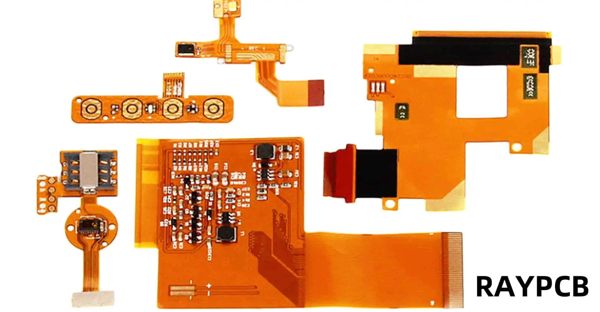
What are Flexible PCBs?

Flexible printed circuit boards, also known as flex PCBs or flexible electronics, are thin, bendable circuit boards that can be shaped to fit into tight spaces or conform to unique product designs. Unlike traditional rigid PCBs, flexible PCBs are made with a flexible base material, typically a plastic film like polyimide, which allows them to bend, fold, and twist without breaking.

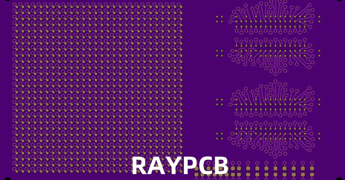
Components of Flexible PCBs

Flexible PCBs consist of several key components:

  1. Base material (substrate)
  2. Conductive layers
  3. Coverlay or protective coating
  4. Adhesives
  5. Circuitry and components
YouTube video

Learn more about:

  1. Flex PCB Stackupย 
  2. Flex PCB Stiffener
  3. Flex PCB Assembly
  4. 6 Layer Flex PCB
  5. 8 Layer Flex PCB

Let’s take a closer look at each of these components:

ComponentDescriptionCommon Materials
Base materialThe flexible substrate that forms the foundation of the PCBPolyimide, Polyester, LCP (Liquid Crystal Polymer)
Conductive layersThin layers of conductive material that form the circuit pathsCopper, Silver, Aluminum
CoverlayA protective layer that insulates and protects the circuitryPolyimide, Epoxy
AdhesivesMaterials used to bond layers togetherAcrylic, Epoxy
Circuitry and componentsThe actual electronic components and traces that make up the circuitVarious metals and electronic components

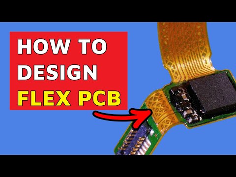
Types of Flexible PCBs

Flexible PCBs come in various types, each designed to meet specific application requirements:

Single-sided Flex PCBs

Single-sided flex PCBs have a single conductive layer on one side of the flexible substrate. They are the simplest and most cost-effective type of flexible PCB.

Double-sided Flex PCBs

Double-sided flex PCBs have conductive layers on both sides of the substrate, allowing for more complex circuit designs and higher component density.

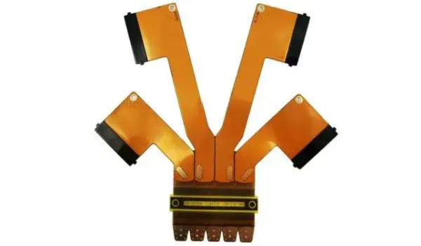
Multilayer Flex PCBs

Multilayer flex PCBs consist of three or more conductive layers, separated by insulating layers. They offer the highest level of circuit density and complexity.

Rigid-Flex PCBs

Rigid-flex PCBs combine both rigid and flexible board technologies in a single circuit board. They feature areas of flexible circuitry connected to rigid board sections.

Here’s a comparison of these types:

TypeComplexityCostFlexibilityApplication Examples
Single-sidedLowLowHighSimple consumer electronics, wearables
Double-sidedMediumMediumMediumSmartphones, tablets
MultilayerHighHighLow-MediumAdvanced medical devices, aerospace equipment
Rigid-FlexVery HighVery HighVariableMilitary equipment, complex industrial machinery

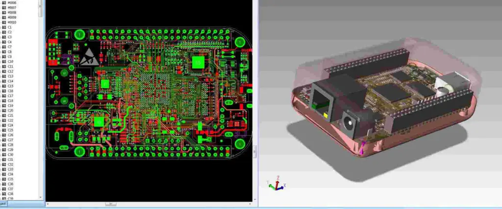
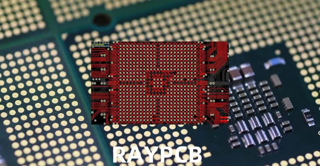
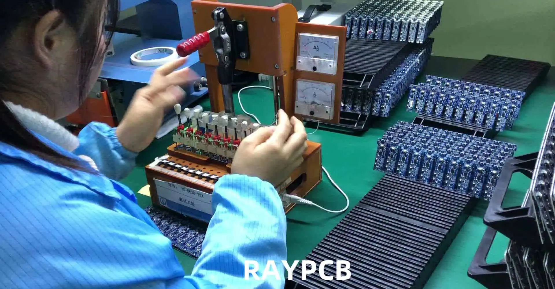
Manufacturing Process of Flexible PCBs

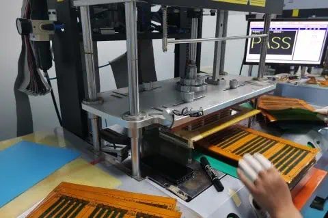
The manufacturing process for flexible PCBs differs from that of rigid PCBs due to the unique materials and requirements involved. Here’s an overview of the main steps:

  1. Material preparation
  2. Imaging and etching
  3. Coverlay application
  4. Drilling and plating
  5. Surface finishing
  6. Assembly and testing

Each of these steps requires specialized equipment and techniques to ensure the flexibility and durability of the final product.

Advantages of Flexible PCBs

Flexible PCBs offer numerous advantages over their rigid counterparts:

1. Space and Weight Savings

Flexible PCBs can be bent, folded, or shaped to fit into tight or irregularly shaped spaces, allowing for more compact and lightweight product designs.

2. Increased Reliability

The ability to flex reduces stress on components and solder joints, potentially increasing the overall reliability and lifespan of the device.

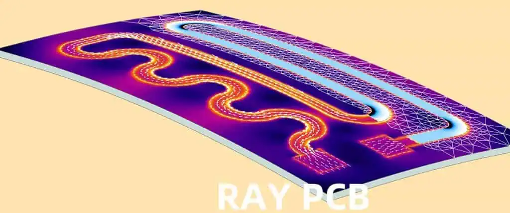
3. Improved Thermal Management

Flexible PCBs can dissipate heat more effectively than rigid boards, which can lead to better thermal management in electronic devices.

4. Enhanced Design Freedom

Designers have more freedom to create unique and innovative product shapes and form factors when using flexible PCBs.

5. Resistance to Vibration and Movement

The flexible nature of these PCBs makes them more resistant to vibration and movement, which is crucial in applications like automotive electronics or wearable devices.

AdvantageDescriptionImpact on Design
Space and Weight SavingsAllows for compact and lightweight designsEnables smaller, more portable devices
Increased ReliabilityReduces stress on components and solder jointsLonger product lifespan, fewer failures
Improved Thermal ManagementBetter heat dissipationEnhanced performance in high-power applications
Enhanced Design FreedomAllows for unique and innovative product shapesEnables creative and ergonomic designs
Resistance to VibrationBetter performance in high-vibration environmentsIdeal for automotive and aerospace applications

Applications of Flexible PCBs

Flexible PCBs have found their way into a wide range of industries and applications:

Consumer Electronics

  • Smartphones and tablets
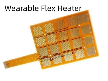
  • Wearable devices (smartwatches, fitness trackers)
  • Digital cameras
  • Flexible displays

Automotive Industry

  • Dashboard electronics
  • Engine control systems
  • Advanced driver assistance systems (ADAS)

Medical Devices

  • Implantable devices
  • Hearing aids
  • Portable diagnostic equipment

Aerospace and Defense

  • Satellite systems
  • Aircraft avionics
  • Military communication devices

Industrial Equipment

Here’s a table summarizing the applications across different industries:

IndustryApplicationsKey Benefits
Consumer ElectronicsSmartphones, wearables, camerasCompact design, lightweight
AutomotiveDashboard electronics, engine controlVibration resistance, space-saving
Medical DevicesImplantables, hearing aidsBiocompatibility, miniaturization
Aerospace and DefenseSatellite systems, avionicsReliability, weight reduction
Industrial EquipmentRobotics, solar panelsDurability, design flexibility

Challenges and Limitations of Flexible PCBs

While flexible PCBs offer many advantages, they also come with their own set of challenges and limitations:

1. Higher Manufacturing Costs

The specialized materials and manufacturing processes required for flexible PCBs often result in higher production costs compared to rigid PCBs.

2. Design Complexity

Designing flexible PCBs requires a different approach and specialized software tools, which can increase the complexity of the design process.

3. Limited Component Options

Not all electronic components are suitable for use with flexible PCBs, which can limit design options in some cases.

4. Durability Concerns

While flexible PCBs are designed to bend, excessive or repeated flexing can potentially lead to fatigue and failure over time.

5. Thermal Management Challenges

Despite improved heat dissipation in some cases, managing heat in densely packed flexible circuits can be challenging.

ChallengeDescriptionPotential Solutions
Higher CostsIncreased production expensesOptimize design for mass production, explore new materials
Design ComplexityRequires specialized approach and toolsInvest in training, use advanced design software
Limited ComponentsNot all components work with flex PCBsDevelop flex-compatible components, creative design solutions
Durability ConcernsPotential fatigue from repeated flexingCareful design of flex zones, use of strain relief
Thermal ManagementHeat dissipation in dense circuitsImproved thermal design, use of heat-spreading materials

Future of Flexible PCBs

The future of flexible PCBs looks promising, with ongoing research and development pushing the boundaries of what’s possible:

Stretchable Electronics

Researchers are working on developing stretchable PCBs that can not only bend but also stretch, opening up new possibilities for wearable and medical devices.

Integration with 3D Printing

Advancements in 3D printing technology may allow for the direct printing of flexible circuits, potentially revolutionizing the manufacturing process.

Improved Materials

New materials are being developed to enhance the performance, durability, and flexibility of PCBs while potentially reducing costs.

Internet of Things (IoT) and Smart Devices

The growth of IoT and smart devices will likely drive further innovation in flexible PCB technology to meet the demand for smaller, more versatile electronics.

Sustainable and Biodegradable PCBs

As environmental concerns grow, there’s increasing research into developing sustainable and even biodegradable flexible PCBs.

Conclusion

Flexible PCBs have indeed revolutionized the electronics industry, enabling the creation of smaller, lighter, and more versatile devices. While they come with their own set of challenges, the advantages they offer in terms of design freedom, reliability, and performance make them an invaluable technology in modern electronics. As research continues and new applications emerge, we can expect to see even more innovative uses of flexible PCBs in the future, further blurring the lines between rigid and flexible electronics.

FAQ

1. Are flexible PCBs more expensive than rigid PCBs?

Yes, flexible PCBs are generally more expensive than rigid PCBs due to the specialized materials and manufacturing processes involved. However, they can offer cost savings in other areas, such as assembly and packaging, due to their space-saving and design flexibility benefits.

2. How durable are flexible PCBs?

Flexible PCBs are designed to be quite durable and can withstand repeated bending and flexing. However, their durability depends on factors such as the materials used, the design of the flex zones, and the specific application. When properly designed and used within their specified parameters, flexible PCBs can be very reliable.

3. Can all electronic components be used with flexible PCBs?

Not all electronic components are suitable for use with flexible PCBs. Some components may be too rigid or heavy, which could cause stress on the flexible substrate. However, many components have been adapted for use with flexible PCBs, and new flex-compatible components are continually being developed.

4. What industries benefit most from flexible PCB technology?

While flexible PCBs have applications across many industries, they are particularly beneficial in consumer electronics, automotive, medical devices, aerospace, and wearable technology. These industries often require compact, lightweight, and uniquely shaped electronic solutions that flexible PCBs can provide.

5. Is it possible to repair a flexible PCB?

Repairing flexible PCBs can be challenging due to their thin and flexible nature. While minor repairs are possible in some cases, it often requires specialized equipment and expertise. In many situations, especially with mass-produced consumer electronics, it may be more practical to replace the entire flexible PCB rather than attempt a repair.

Electroplated Nickel Process for PCB Printed Circuit Boards

Electroplated nickel has become an integral part of modern printed circuit board (PCB) manufacturing, offering enhanced durability, conductivity, and corrosion resistance. This comprehensive guide explores the technical aspects, processes, and considerations involved in nickel electroplating for PCBs, providing manufacturers and engineers with essential information for optimal implementation.

YouTube video

Understanding Nickel Electroplating Fundamentals

Basic Principles of Electroplating

Electroplating is an electrochemical process where metal ions in solution are reduced to their metallic form on a conductive substrate. In PCB manufacturing, nickel electroplating involves depositing a controlled thickness of nickel onto copper traces and pads, creating a robust protective and functional layer.

Chemical Composition of Plating Solutions

The success of nickel electroplating largely depends on the composition of the plating bath. Modern nickel plating solutions typically contain:

ComponentConcentration RangeFunction
Nickel Sulfate200-300 g/LPrimary source of nickel ions
Nickel Chloride30-60 g/LImproves anode dissolution
Boric Acid30-45 g/LpH buffer
Brighteners0.5-2 mL/LEnhance deposit appearance
Levelers1-3 mL/LImprove thickness distribution

Process Parameters and Control

Critical Operating Conditions

Maintaining precise control over operating parameters is essential for achieving high-quality nickel deposits:

ParameterOptimal RangeImpact on Quality
Temperature50-65ยฐCAffects deposit stress and brightness
pH3.5-4.5Influences deposit properties
Current Density2-10 A/dmยฒDetermines plating rate and quality
AgitationModerate-HighEnsures uniform distribution

Process Steps

1. Surface Preparation

  • Cleaning and degreasing
  • Microetching
  • Acid activation

2. Plating Process

  • Initial current ramping
  • Steady-state plating
  • Final thickness verification

3. Post-Treatment

  • Rinse cycles
  • Anti-tarnish application
  • Quality inspection

Advanced Technical Considerations

Deposit Properties and Specifications

PropertyTypical RangeTesting Method
Thickness2-5 ยตmX-ray fluorescence
Hardness400-500 HVMicrohardness testing
Purity>99.5%Chemical analysis
Internal Stress10-40 MPaDeposit stress analyzer

Common Defects and Solutions

Defect TypePossible CausesRemedial Actions
Poor AdhesionSurface contaminationImprove cleaning process
PittingLow agitationIncrease solution movement
BurningExcessive current densityAdjust current parameters
Stress PeelingHigh internal stressModify brightener levels

Equipment and Infrastructure Requirements

Basic Setup Components

  1. Plating tanks (PP or PVC lined)
  2. Filtration systems
  3. Temperature control units
  4. Rectifiers and power supplies
  5. Agitation mechanisms

Advanced Control Systems

Control ParameterMonitoring MethodControl Range
Bath TemperatureRTD sensorsยฑ1ยฐC
pH LevelOnline pH metersยฑ0.1 units
Solution LevelLevel sensorsยฑ5mm
Current DistributionHull cell analysisWeekly check

Environmental and Safety Considerations

PCB Plated Through Hole Manufacturing Processes

Waste Treatment Requirements

Waste StreamTreatment MethodDisposal Criteria
Spent SolutionIon exchange<5 ppm Ni
Rinse WaterReverse osmosispH 6-9
Filter CakeStabilizationLandfill compatible

Safety Protocols

  1. Personal protective equipment requirements
  2. Ventilation specifications
  3. Emergency response procedures
  4. Chemical handling guidelines

Quality Control and Testing

Testing Requirements

Test TypeFrequencyAcceptance Criteria
ThicknessEvery lotยฑ10% of specification
AdhesionDailyNo peeling at 90ยฐ bend
Surface FinishEvery shiftRa โ‰ค 0.5 ยตm
PorosityWeeklyZero defects

Documentation and Traceability

  • Batch records
  • Process control charts
  • Equipment maintenance logs
  • Operator training records

Cost Considerations

Operating Costs Breakdown

Cost ComponentPercentage of TotalControl Measures
Chemistry25-30%Bath maintenance
Labor20-25%Process automation
Energy15-20%Efficiency optimization
Waste Treatment10-15%Recovery systems
Maintenance10-15%Preventive programs

Process Optimization Strategies

Key Performance Indicators

KPITarget RangeImprovement Actions
First Pass Yield>95%Process control
Plating Rate0.5-1.0ยตm/minCurrent optimization
Chemical Consumption<10% variationBath analysis
Energy Efficiency>80%Equipment maintenance

Future Trends and Developments

Emerging Technologies

  1. Pulse plating techniques
  2. Advanced brightener systems
  3. Automated process control
  4. Environmental-friendly alternatives

Frequently Asked Questions (FAQ)

Q1: What is the optimal thickness for nickel plating on PCB components?

A1: The optimal thickness typically ranges from 2 to 5 micrometers, depending on the application. Critical factors include the expected operating environment, mechanical stress requirements, and subsequent plating layers. For most commercial applications, 3 micrometers provides adequate protection and performance.

Q2: How can I prevent nickel plating adhesion failures?

A2: Adhesion failures can be prevented through proper surface preparation, including thorough cleaning, microetching, and acid activation. Maintaining optimal bath chemistry and ensuring proper current distribution are also critical. Regular Hull cell testing helps identify potential adhesion issues before they occur in production.

Q3: What are the main factors affecting nickel deposit stress?

A3: The primary factors affecting nickel deposit stress include:

  • Bath temperature
  • Current density
  • pH level
  • Brightener concentration
  • Impurity levels Controlling these parameters within specified ranges helps minimize internal stress in the deposit.

Q4: How often should the plating bath be analyzed and maintained?

A4: Complete bath analysis should be performed weekly, with basic parameters (pH, temperature, specific gravity) checked daily. Brightener analysis should be conducted every shift, and carbon treatment should be performed monthly or as needed based on organic contamination levels.

Q5: What are the environmental considerations for nickel plating operations?

A5: Key environmental considerations include:

  • Proper waste treatment and disposal
  • Recovery and recycling of nickel from rinse waters
  • Emission control through adequate ventilation
  • Compliance with local environmental regulations
  • Implementation of closed-loop recovery systems

Eagle DRC and Gerber Files: A Complete Guide

Autodesk EAGLE is a powerful PCB design software that includes essential features for ensuring design quality through Design Rule Check (DRC) and manufacturing preparation via Gerber file generation. This comprehensive guide explores both aspects in detail, providing crucial information for PCB designers and engineers.

Understanding Design Rule Check (DRC)

DRC Fundamentals

DRC AspectDescriptionImportance
Clearance RulesMinimum spacing requirementsPrevents shorts
Width RulesTrace width specificationsEnsures current capacity
Drill RulesHole size and spacingManufacturing feasibility
Mask RulesSolder mask parametersAssembly quality

Types of Design Rules

Electrical Rules

drc pcb
Rule TypeParametersCommon Values
ClearanceMin spacing between elements6-10 mil
WidthMin/max trace width8-12 mil
Drill SizeMin/max hole diameter0.3-0.4 mm
Annular RingMin copper around holes0.15-0.25 mm

Manufacturing Rules

CategoryParametersPurpose
Layer SetupStack definitionMaterial specification
Mask ClearanceSolder mask openingsComponent soldering
Minimum FeatureSmallest allowed featureManufacturability
Board EdgeEdge clearancesBoard integrity

Setting Up DRC in Eagle

Basic Setup Process

  1. Access Configuration
    • Open DRC dialog
    • Select rule categories
    • Input parameters
    • Save configuration
  2. Custom Rules Creation
    • Define specific requirements
    • Set layer-specific rules
    • Configure special areas
    • Establish exceptions

Running DRC Checks

Check Categories

CategoryElements CheckedCommon Issues
ClearanceComponent spacingOverlapping traces
ConnectivitySignal continuityUnconnected nets
Layer UsageLayer assignmentsIncorrect routing
Size LimitsFeature dimensionsUndersized elements

Error Resolution

Common Errors

Error TypePossible CauseSolution
Clearance ViolationToo close spacingAdjust component placement
Width ErrorIncorrect trace widthModify trace properties
Drill ErrorInvalid hole sizeUpdate drill parameters
Mask ErrorIncorrect mask setupAdjust mask settings

Gerber File Generation

Gerber File Basics

File TypeExtensionPurpose
Top Copper.GTLComponent side copper
Bottom Copper.GBLSolder side copper
Top Mask.GTSComponent side mask
Bottom Mask.GBSSolder side mask
Silkscreen.GTO/.GBOComponent marking
Drill File.TXTHole locations

Layer Configuration

Essential Layers

Layer NameNumberContent
Top Layer1Components and traces
Bottom Layer16Bottom side traces
Pads17Through-hole pads
Vias18Through-board connections
Dimension20Board outline

Export Settings

ParameterRecommended ValuePurpose
FormatRS-274XIndustry standard
UnitsInchesManufacturing preference
Resolution2:04Coordinate precision
OptimizeYesFile size reduction

Advanced DRC Configuration

view-gerber-files

Custom Rule Creation

  1. Specialized Rules
    • High-speed signals
    • Power distribution
    • RF considerations
    • Flex PCB requirements
  2. Rule Priority
    • Global rules
    • Net class rules
    • Component rules
    • Area rules

DRC Script Implementation

Script ElementFunctionApplication
Rule DefinitionParameter setupBasic rules
Conditional RulesSpecific casesSpecial requirements
Error HandlingIssue managementProblem resolution
DocumentationRule documentationReference material

Gerber File Verification

Pre-Manufacturing Checks

Visual Verification

Check TypeElements to VerifyTools Used
Layer AlignmentRegistration marksGerber viewer
Feature SizeMinimum dimensionsMeasurement tools
Text ReadabilitySilkscreen qualityPreview mode
Hole PositionDrill file accuracyOverlay view

Manufacturing Preparation

  1. File Organization
    • Logical naming
    • Layer grouping
    • Version control
    • Documentation
  2. Manufacturing Notes
    • Board specifications
    • Special requirements
    • Material details
    • Finish options

Best Practices

DRC Implementation

PracticeDescriptionBenefit
Regular ChecksFrequent DRC runsEarly error detection
Custom RulesProject-specific setupDesign optimization
DocumentationRule documentationKnowledge transfer
Version ControlRule set managementConsistency

Gerber Generation

Quality Assurance Steps

  1. Pre-Generation
    • Design verification
    • Layer confirmation
    • Rule compliance
    • Component check
  2. Post-Generation
    • File completeness
    • Layer accuracy
    • Dimension verification
    • Manufacturing review

Advanced Features

Automation Capabilities

FeatureFunctionApplication
Batch DRCMultiple checksLarge designs
Custom ScriptsAutomated tasksRepetitive processes
Report GenerationDocumentationQuality assurance
IntegrationThird-party toolsExtended functionality

Special Considerations

  1. High-Speed Design
  2. Mixed Technology
    • Through-hole compatibility
    • SMT requirements
    • Hybrid assembly
    • Special processes

Future Developments

Industry Trends

  1. Software Evolution
    • AI integration
    • Cloud capabilities
    • Real-time collaboration
    • Enhanced automation
  2. Manufacturing Integration
    • Direct output
    • Smart verification
    • Process optimization
    • Quality improvement

Frequently Asked Questions (FAQ)

Q1: What are the most critical DRC rules to set in Eagle?

The most critical DRC rules include:

  • Clearance between copper elements (minimum 6-10 mil)
  • Minimum trace width (typically 8-12 mil)
  • Minimum drill size (usually 0.3mm)
  • Annular ring size (minimum 0.15mm) These values may vary based on your manufacturer’s capabilities.

Q2: Why do I get many DRC errors after importing a component?

Common causes include:

  • Incompatible footprint design
  • Different design rule settings
  • Layer assignment issues
  • Component library problems Always verify component libraries and design rules match your project requirements.

Q3: How can I verify my Gerber files are correct before sending them to manufacturing?

Use these steps:

  1. View files in a Gerber viewer
  2. Check all layer alignments
  3. Verify board dimensions
  4. Confirm drill file accuracy
  5. Compare against original design

Q4: What’s the difference between outline and dimension layers in Gerber export?

The dimension layer (20) defines the physical board outline for manufacturing, while outline layers can be used for documentation or assembly information. Always use the dimension layer for the actual board outline in Gerber export.

Q5: How often should I run DRC checks during PCB design?

Best practices recommend:

  • After placing major components
  • During routing (incremental checks)
  • Before starting a new design section
  • Before generating Gerber files
  • After any significant design changes Regular checks help catch issues early in the design process.

DipTrace and Gerber Export: A Comprehensive Guide

DipTrace is a powerful PCB design software suite that enables engineers and designers to create professional-grade printed circuit boards. One of its crucial features is the ability to export designs to Gerber format, the de facto standard for PCB manufacturing. This comprehensive guide explores DipTrace’s capabilities and the intricacies of Gerber file export.

Understanding DipTrace

Key Components of DipTrace

ModulePrimary FunctionKey Features
SchematicCircuit designComponent placement, wire routing
PCB LayoutBoard designTrack routing, copper pour
Component EditorPart creationPin configuration, package design
Pattern EditorFootprint designPad creation, dimension setup

DipTrace Interface Overview

Main Features

Feature CategoryDescriptionCommon Uses
Design ToolsDrawing and editing toolsComponent placement, routing
Verification ToolsDesign rule checkingError detection, validation
Library ManagementComponent organizationPart selection, creation
Export ToolsFile generationManufacturing output

DipTrace Advantages

  1. User Interface Benefits
    • Intuitive design
    • Customizable workspace
    • Easy navigation
    • Context-sensitive menus
  2. Technical Capabilities
    • Multi-layer board support
    • Advanced routing options
    • Real-time DRC
    • 3D visualization

Understanding Gerber Format

Gerber File Basics

AspectDescriptionImportance
File FormatVector formatIndustry standard
Data StructureLayer-basedManufacturing accuracy
File TypesRS-274X, RS-274DCompatibility
Extensions.gbr, .gerFile identification

Gerber Layer Types

Essential Layers

Layer TypeExtensionPurpose
Top Copper.GTLComponent connections
Bottom Copper.GBLBottom layer traces
Top Solder Mask.GTSSolder protection
Bottom Solder Mask.GBSBottom protection
Silkscreen Top.GTOComponent markings
Silkscreen Bottom.GBOBottom markings
Drill File.TXTHole locations

Gerber Export Process in DipTrace

Pre-Export Preparation

  1. Design Verification
    • Run DRC checks
    • Verify component placement
    • Check copper clearances
    • Validate hole sizes
  2. Layer Setup
    • Confirm layer stack
    • Verify layer names
    • Check layer visibility
    • Set layer polarities

Export Configuration

Basic Settings

SettingDescriptionRecommended Value
UnitsMeasurement systemMM (recommended)
FormatCoordinate format2:4 or 4:4
ZerosZero handlingLeading removed
ExtensionsFile extensionsStandard Gerber

Advanced Options

OptionPurposeUsage
AperturesDefine shapesComponent outlines
D-CodesTool definitionsManufacturing tools
G-CodesCommand codesMovement instructions

Step-by-Step Export Process

  1. Initial Setup
    • Open PCB Layout
    • Select File โ†’ Export
    • Choose Gerber format
  2. Layer Selection
    • Select required layers
    • Configure layer options
    • Set output directory
  3. Parameter Configuration
    • Set units and precision
    • Configure file format
    • Define aperture table
  4. Generation and Verification
    • Generate files
    • Verify output
    • Check file completeness

Best Practices for Gerber Export

File Organization

CategoryRecommendationPurpose
Naming ConventionConsistent systemEasy identification
Folder StructureOrganized hierarchyFile management
Version ControlRevision trackingChange management

Quality Assurance

  1. Pre-Export Checks
    • Design rule compliance
    • Layer alignment
    • Component clearance
    • Copper pour verification
  2. Post-Export Verification
    • File completeness
    • Layer accuracy
    • Dimension verification
    • Drill file correlation

Common Export Issues and Solutions

Troubleshooting Guide

IssuePossible CauseSolution
Missing LayersIncorrect selectionReview layer setup
Misaligned ElementsCoordinate errorsCheck origin point
Incomplete FeaturesExport settingsAdjust parameters
File Generation ErrorsSoftware conflictsReset preferences

Prevention Strategies

  1. Regular Verification
    • Periodic DRC runs
    • Layer checks
    • Component verification
    • Export settings review
  2. Documentation
    • Keep export logs
    • Document settings
    • Maintain procedure guides
    • Track changes

Advanced Gerber Features in DipTrace

Custom Aperture Definition

FeatureUse CaseBenefits
Complex ShapesSpecial componentsManufacturing accuracy
Custom SizesUnique requirementsDesign flexibility
Macro DefinitionsRepeated elementsEfficiency

Automation Options

  1. Script-Based Export
    • Batch processing
    • Automated checks
    • Custom parameters
    • Multiple outputs
  2. Integration Features
    • CAM tool compatibility
    • Manufacturing links
    • Quality verification
    • Documentation generation

Future Developments and Industry Trends

Emerging Technologies

  1. Format Evolution
    • New specifications
    • Enhanced features
    • Better integration
    • Improved accuracy
  2. Software Improvements
    • AI-assisted design
    • Cloud integration
    • Real-time verification
    • Enhanced automation

Frequently Asked Questions (FAQ)

Q1: Why are my Gerber files missing some PCB features?

This usually occurs due to incorrect layer selection or export settings. Ensure all necessary layers are selected and properly configured in the export dialog. Also, verify that all features are on their correct layers in the PCB design.

Q2: How can I verify my Gerber files before sending them to manufacturing?

Use a Gerber viewer software to check all layers, ensure proper alignment, and verify dimensions. Popular viewers include GerbView, CAM350, or online viewers provided by PCB manufacturers. DipTrace also includes a built-in preview feature.

Q3: What’s the difference between RS-274X and RS-274D Gerber formats?

RS-274X is the newer, extended format that includes aperture definitions within the file, making it more self-contained. RS-274D is older and requires separate aperture files. DipTrace primarily uses RS-274X for better compatibility with modern manufacturing processes.

Q4: Why do I need to include a drill file with my Gerber files?

The drill file (.TXT or .XLN) contains essential information about hole locations, sizes, and types that isn’t included in the Gerber layers. This file is crucial for the PCB manufacturer to properly drill all holes in your board.

Q5: How can I optimize my Gerber export process for complex boards?

Create a checklist including:

  • Layer verification
  • DRC completion
  • Export settings confirmation
  • File naming conventions
  • Post-export verification This ensures consistency and reduces errors in the export process.

The Complete Guide to PCB vs Integrated Circuit: Understanding Their Differences and Applications

In the realm of electronic components and circuit design, Printed Circuit Boards (PCBs) and Integrated Circuits (ICs) are fundamental elements that have revolutionized modern electronics. While both serve crucial roles in electronic devices, they differ significantly in their design, functionality, and applications. This comprehensive guide explores the key differences between PCBs and ICs, their manufacturing processes, applications, and the crucial role they play in modern electronics.

Understanding PCB (Printed Circuit Board)

Definition and Basic Structure

A Printed Circuit Board (PCB) is a flat board made of non-conductive material that provides mechanical support and electrical connections for electronic components through conductive pathways, or traces, etched from copper sheets laminated onto the board.

Key Components of a PCB

Layer Description Function
Substrate Non-conductive base material Provides mechanical support
Copper Layer Conductive material Creates electrical pathways
Solder Mask Protective layer Prevents short circuits
Silkscreen Text and symbols Component identification

Types of PCBs

Based on Layer Count

Type Description Common Applications
Single-layer One copper layer Simple electronics, LED lights
Double-layer Two copper layers Consumer electronics
Multi-layer 4+ copper layers Complex devices, computers

Based on Flexibility

  1. Rigid PCBs
    • Most common type
    • Used in standard electronic devices
    • Provides excellent mechanical stability
  2. Flexible PCBs
    • Can be bent or flexed
    • Used in compact devices
    • Ideal for dynamic applications
  3. Rigid-Flex PCBs
    • Combines rigid and flexible sections
    • Used in complex 3D applications
    • Provides design flexibility

Understanding Integrated Circuits (ICs)

Definition and Basic Structure

An Integrated Circuit is a miniaturized electronic circuit containing thousands or millions of electronic components (transistors, resistors, capacitors) fabricated on a single semiconductor material, typically silicon.

Components of an IC

Component Function Scale
Transistors Switching and amplification Nanometer scale
Resistors Current control Microscopic
Capacitors Energy storage Microscopic
Interconnects Signal routing Nanometer scale

Types of ICs

Based on Function

Type Description Applications
Digital ICs Process binary signals Computers, digital devices
Analog ICs Process continuous signals Audio equipment, sensors
Mixed-signal ICs Combine digital and analog Mobile phones, IoT devices

Based on Integration Level

Xilinx Artix 7
Xilinx Artix 7
  1. Small-Scale Integration (SSI)
    • Up to 100 components
    • Basic logic gates
    • Simple functions
  2. Medium-Scale Integration (MSI)
    • 100-1000 components
    • Counters, multiplexers
    • Moderate complexity
  3. Large-Scale Integration (LSI)
    • 1000-100,000 components
    • Microprocessors
    • Complex functions
  4. Very Large-Scale Integration (VLSI)
    • Over 100,000 components
    • Modern processors
    • Highly complex systems

Key Differences Between PCBs and ICs

Physical Characteristics

Characteristic PCB IC
Size Typically larger (cm to m) Very small (ฮผm to mm)
Component Integration External components mounted Components built into silicon
Flexibility Can be rigid or flexible Always rigid
Repairability Generally repairable Usually not repairable

Manufacturing Process

PCB Manufacturing Steps

  1. Design Phase
    • Circuit schematic creation
    • Component layout
    • Routing design
  2. Production Phase
    • Copper coating
    • Photolithography
    • Etching
    • Layer lamination
    • Drilling
    • Surface finishing

IC Manufacturing Steps

  1. Design Phase
    • Circuit design
    • Layout design
    • Verification
  2. Production Phase
    • Wafer preparation
    • Photolithography
    • Ion implantation
    • Metal deposition
    • Testing
    • Packaging

Cost Comparison

Aspect PCB IC
Initial Setup Cost Lower Very high
Per-unit Cost (High Volume) Moderate Low
Prototype Cost Low Very high
Modification Cost Low Very high

Applications and Use Cases

PCB Applications

  1. Consumer Electronics
    • Smartphones
    • Laptops
    • Home appliances
  2. Industrial Equipment
    • Control systems
    • Manufacturing equipment
    • Power supplies
  3. Automotive Electronics
    • Engine control units
    • Entertainment systems
    • Safety systems

IC Applications

  1. Computing Devices
    • Microprocessors
    • Memory chips
    • Graphics processors
  2. Communication Equipment
  3. Specialized Applications
    • Medical devices
    • Military equipment
    • Aerospace systems

Future Trends and Developments

PCB Future Trends

  1. Advanced Materials
    • High-frequency materials
    • Flexible substrates
    • Environmental-friendly materials
  2. Manufacturing Technologies
    • 3D printing
    • Additive manufacturing
    • Automated assembly

IC Future Trends

  1. Scaling Technologies
    • Smaller process nodes
    • 3D integration
    • New materials
  2. Emerging Technologies
    • Quantum computing
    • Neuromorphic computing
    • Photonic integrated circuits

Frequently Asked Questions (FAQ)

Q1: Can PCBs contain ICs?

Yes, PCBs often serve as the platform for mounting and connecting multiple ICs along with other electronic components. The PCB provides the necessary interconnections between ICs and other components while offering mechanical support.

Q2: Why can’t ICs be repaired like PCBs?

ICs cannot typically be repaired because their components are microscopic and integrated into a single piece of semiconductor material. PCBs, on the other hand, have larger, discrete components that can be replaced individually.

Q3: Which is more cost-effective for mass production?

For mass production, ICs are generally more cost-effective per unit despite having higher initial setup costs. PCBs have lower setup costs but higher per-unit costs in large volumes.

Q4: Can PCBs be designed without ICs?

Yes, Prototype PCBs can be designed using discrete components without ICs, but modern electronic devices typically use a combination of both for optimal performance and functionality.

Q5: What determines the choice between using a PCB or an IC for a specific function?

The choice depends on factors such as:

  • Production volume
  • Cost constraints
  • Performance requirements
  • Space limitations
  • Power consumption requirements
  • Time to market

Brief Talk About Heat Dissipation Of Aluminum PCB and Its Design Method

Aluminum PCBs (Metal Core PCBs or MCPCBs) have become increasingly important in high-power electronic applications due to their superior thermal management capabilities. This article explores the fundamentals of heat dissipation in aluminum PCBs and presents comprehensive design methodologies for optimal thermal performance.

Fundamentals of Aluminum PCB Construction

Material Layer Structure

LayerMaterialTypical ThicknessThermal Conductivity
Top LayerCopper35-70ฮผm398 W/mยทK
DielectricThermally Conductive75-150ฮผm1-7 W/mยทK
Base LayerAluminum0.8-3.0mm237 W/mยทK
Surface FinishHASL/ENIG3-15ฮผmVaries

Thermal Properties Comparison

Material TypeThermal Conductivity (W/mยทK)Cost FactorWeight Factor
FR-40.2-0.311
Aluminum PCB1.0-7.02.0-3.01.5-2.0
Ceramic PCB20-2704.0-8.02.0-3.0
Copper Core3985.0-10.02.5-3.5

Heat Dissipation Mechanisms

heat dissipation in electronic devices

Primary Heat Transfer Methods

MethodContributionEfficiency Factor
Conduction60-70%High
Convection20-30%Medium
Radiation5-10%Low

Thermal Resistance Path

Path ComponentTypical Range (ยฐC/W)Optimization Method
Junction to Case0.5-3.0Die attach material
Case to Board1.0-5.0Thermal interface
Board to Ambient5.0-20.0Cooling solution

Design Methodologies

Component Layout Guidelines

Thermal Spacing Requirements

Component PowerMinimum SpacingRecommended Spacing
<1W2mm5mm
1-3W5mm10mm
3-5W10mm15mm
>5W15mm20mm

Copper Design Rules

FeatureSpecificationPurpose
Minimum Width0.2mmCurrent capacity
Thermal Relief0.3mmAssembly control
Thermal Via Diameter0.3-0.5mmHeat transfer
Via Spacing1.0-1.5mmThermal distribution

Thermal Design Considerations

Thermal Via Implementation

ParameterValueNotes
Via Diameter0.3-0.5mmPlated through-hole
Via Spacing1.0-1.5mmGrid pattern
Plating Thickness25ฮผmMinimum
Fill TypeSolid/PasteApplication dependent

Thermal Pattern Design

Pattern TypeThermal EfficiencyCost Impact
Solid Plane100%Baseline
Grid Pattern80-90%-10%
Star Pattern70-80%-20%
Custom Pattern60-95%Varies

Performance Optimization

Thermal Management Solutions

Solution TypeHeat DissipationCost ImpactIntegration Complexity
Heat SinkUp to 70%MediumMedium
Forced AirUp to 85%HighHigh
Thermal PasteUp to 30%LowLow
Liquid CoolingUp to 95%Very HighVery High

Material Selection Guidelines

ComponentRecommended MaterialThermal ConductivityCost Factor
Base MaterialAL5052138 W/mยทK1
DielectricHigh Tg Epoxy1.0-7.0 W/mยทK1.5-3.0
Thermal InterfaceSilicone Based3.0-5.0 W/mยทK2.0-4.0
Surface FinishENIGN/A1.5-2.0

Manufacturing Considerations

Process Parameters

Process StepTemperature RangeTime DurationCritical Parameters
Preheating150-170ยฐC60-90sRamp rate
Soldering230-250ยฐC30-60sPeak temperature
Cooling4ยฐC/s maxN/ACooling rate

Quality Control Methods

Test TypeMethodAcceptance Criteria
Thermal ResistanceASTM D5470โ‰ค0.4ยฐC/W
Dielectric StrengthASTM D149โ‰ฅ3kV
Thermal Cycling-40 to +125ยฐC1000 cycles
Thermal Shock-65 to +150ยฐC300 cycles

Performance Evaluation

Thermal Testing Methods

Test MethodParameters MeasuredEquipment Required
IR ScanningSurface temperatureThermal camera
ThermocouplePoint temperatureData logger
Thermal ResistanceOverall performanceThermal tester
CFD AnalysisAirflow patternsSoftware

Performance Metrics

MetricTarget RangeCritical Factor
Junction Temperatureโ‰ค125ยฐCComponent reliability
Thermal Resistanceโ‰ค0.4ยฐC/WHeat dissipation
Temperature Riseโ‰ค40ยฐCSystem performance
Temperature Uniformityยฑ5ยฐCThermal stress

Frequently Asked Questions

Q1: What are the key advantages of using aluminum PCBs over traditional FR-4 boards?

A1: Aluminum PCBs offer several significant advantages:

  • Superior thermal conductivity (1.0-7.0 W/mยทK vs 0.2-0.3 W/mยทK for FR-4)
  • Better dimensional stability at high temperatures
  • Enhanced reliability for high-power applications
  • Reduced need for additional cooling solutions
  • Longer lifespan of components due to better heat management

Q2: How can thermal via design be optimized for maximum heat dissipation?

A2: Optimal thermal via design involves several key considerations:

  • Via diameter should be 0.3-0.5mm for best performance
  • Grid pattern spacing of 1.0-1.5mm is recommended
  • Copper plating thickness should be minimum 25ฮผm
  • Consider filled vias for better thermal conductivity
  • Implement proper via pattern beneath high-power components

Q3: What are the critical factors in selecting dielectric materials for aluminum PCBs?

A3: Critical factors include:

  • Thermal conductivity (higher is better)
  • Dielectric strength (minimum 3kV)
  • Glass transition temperature (Tg)
  • Thermal expansion coefficient
  • Cost considerations
  • Manufacturing compatibility

Q4: How does component placement affect thermal performance?

A4: Component placement significantly impacts thermal performance through:

  • Spacing between high-power components
  • Proximity to board edges
  • Air flow considerations
  • Thermal interaction between components
  • Access for additional cooling solutions

Q5: What are the common failure modes in aluminum PCBs and how can they be prevented?

A5: Common failure modes and prevention methods include:

  • Delamination (use proper material selection and processing)
  • Thermal stress (implement proper thermal relief design)
  • Solder joint failure (use appropriate thermal profiles)
  • Warpage (consider CTE matching in design)
  • Dielectric breakdown (select appropriate dielectric material)

Conclusion

Aluminum PCB design for optimal heat dissipation requires careful consideration of material selection, layout design, and manufacturing processes. Success depends on understanding thermal management principles and implementing appropriate design methodologies. Regular testing and validation ensure that thermal performance meets design requirements. As power densities continue to increase, the importance of effective thermal management in aluminum PCBs will only grow.

BGA Solderability Standard: Comprehensive Guidelines and Requirements

Ball Grid Array (BGA) solderability is crucial for ensuring reliable electronic assemblies. This comprehensive guide covers industry standards, testing methods, acceptance criteria, and best practices for BGA soldering processes. Understanding and implementing these standards is essential for achieving high-quality, reliable electronic assemblies.

Industry Standards Overview

Applicable Standards

StandardDescriptionScope
IPC-A-610Acceptability of Electronic AssembliesGeneral assembly requirements
J-STD-001Requirements for Soldered Electrical AssembliesSoldering requirements
IPC/JEDEC J-STD-020Moisture Sensitivity ClassificationPackage handling
IPC-7095Design and Assembly Process Implementation for BGAsBGA-specific guidelines

BGA Solder Ball Specifications

Physical Requirements

Ball Dimension Standards

Ball DiameterPitchTolerancePackage Size
0.30mm0.50mmยฑ0.02mmโ‰ค15mm ร— 15mm
0.35mm0.65mmยฑ0.02mmโ‰ค17mm ร— 17mm
0.45mm0.80mmยฑ0.025mmโ‰ค23mm ร— 23mm
0.60mm1.00mmยฑ0.03mmโ‰ค27mm ร— 27mm

Material Composition

TypeCompositionMelting PointApplication
SAC305Sn96.5/Ag3.0/Cu0.5217-220ยฐCLead-free standard
SAC405Sn95.5/Ag4.0/Cu0.5217-220ยฐCHigher reliability
SnPbSn63/Pb37183ยฐCLegacy systems
SAC105Sn98.5/Ag1.0/Cu0.5217-220ยฐCCost-effective

Solderability Requirements

Surface Finish Compatibility

Surface FinishCompatibility RatingShelf LifeComments
ENIGExcellent12 monthsPreferred choice
HASLGood6 monthsTraditional option
OSPGood3-6 monthsCost-effective
Immersion TinVery Good6 monthsGood wettability
ENEPIGExcellent12 monthsHigh reliability

Wettability Requirements

ParameterSpecificationTest Method
Wetting Timeโ‰ค1.5 secondsIPC-J-STD-003
Wetting Forceโ‰ฅ0.3N/mmIPC-TM-650
Contact Angleโ‰ค45 degreesVisual inspection
Coverageโ‰ฅ95%X-ray inspection

Process Parameters

Reflow Profile Requirements

Profile ZoneTemperatureTimeRate
Preheat150-180ยฐC60-120s1-3ยฐC/s
Soak180-200ยฐC60-120sN/A
Reflow230-250ยฐC30-90sN/A
Peak245-260ยฐC10-30sN/A
CoolingBelow 180ยฐCN/A-4ยฐC/s max

Environmental Conditions

ParameterRequirementTolerance
Humidity30-60% RHยฑ5%
Temperature20-26ยฐCยฑ2ยฐC
Oxygen Level<1000ppmยฑ100ppm
Air Flow0.5-2.0 m/sยฑ0.2 m/s

Quality Assessment

Inspection Criteria

X-ray Inspection Standards

Defect TypeAcceptance CriteriaInspection Method
Voids<25% total areaX-ray
BridgingNone allowedX-ray/Visual
Misalignment<25% of ball diameterX-ray
Ball Shape75-125% nominal heightX-ray

Reliability Testing Requirements

Test TypeConditionsDurationAcceptance Criteria
Temperature Cycling-40ยฐC to +125ยฐC1000 cyclesNo failures
Drop Test1500G, 0.5ms30 dropsNo electrical discontinuity
Vibration10-100Hz30 minutesNo failures
HAST130ยฐC/85%RH96 hoursNo electrical failures

Defect Classification

x ray inspection
x ray inspection

Common Defects Categories

CategoryDescriptionAcceptance Level
Class 1Process IndicatorAcceptable
Class 2Minor DefectLimited acceptance
Class 3Major DefectNot acceptable
Class 4Critical DefectNot acceptable

Specific Defect Criteria

Defect TypeClass 2 LimitClass 3 Limit
Void Size<25%<15%
Misalignment<25%<15%
Solder BallNoneNone
Head-on-PillowNoneNone

Process Control Methods

Statistical Process Control Parameters

ParameterControl LimitAction Limit
Peak Temperatureยฑ5ยฐCยฑ8ยฐC
Reflow Timeยฑ5sยฑ10s
Cooling Rateยฑ0.5ยฐC/sยฑ1ยฐC/s
Void Contentยฑ5%ยฑ8%

Documentation Requirements

Document TypeUpdate FrequencyRetention Period
Process ParametersPer lot2 years
Inspection ResultsPer board3 years
Calibration RecordsMonthly2 years
Training RecordsSemi-annual3 years

Troubleshooting Guide

Common Issues and Solutions

IssuePossible CausesCorrective Actions
Excessive VoidingInsufficient preheatAdjust profile
Poor WettingContaminated surfaceClean/replace finish
BridgingExcessive pasteAdjust stencil design
Head-on-PillowPoor thermal profileOptimize profile

Frequently Asked Questions

Q1: What are the critical factors affecting BGA solderability?

A1: The critical factors include:

  • Surface finish quality and compatibility
  • Reflow profile parameters
  • Component storage and handling
  • PCB pad design and finish
  • Solder paste composition and volume
  • Environmental conditions during assembly

Q2: How can void content in BGA solder joints be minimized?

A2: Void content can be minimized through:

  • Optimized reflow profile with adequate soak time
  • Proper solder paste selection and storage
  • Appropriate stencil design and aperture size
  • Controlled atmosphere reflow (nitrogen)
  • Proper pad design and surface finish
  • Regular maintenance of reflow equipment

Q3: What are the acceptable criteria for BGA solder joint inspection?

A3: Acceptable criteria include:

  • Void content less than 25% of total joint area
  • Complete wetting around ball circumference
  • No bridging between adjacent balls
  • Proper ball collapse height
  • No evidence of head-on-pillow defects
  • Proper alignment within 25% of ball diameter

Q4: How does surface finish selection impact BGA solderability?

A4: Surface finish selection impacts:

  • Initial wettability
  • Shelf life of PCB
  • Intermetallic compound formation
  • Long-term reliability
  • Process window flexibility
  • Overall assembly cost

Q5: What are the key considerations for BGA reflow profiling?

A5: Key considerations include:

  • Package size and thermal mass
  • Maximum temperature ratings
  • Solder paste requirements
  • PCB thickness and complexity
  • Component mix on the board
  • Required throughput speed

Conclusion

Maintaining high standards for BGA solderability is essential for producing reliable electronic assemblies. Following these guidelines and standards helps ensure consistent quality and reliability in BGA assembly processes. Regular monitoring, documentation, and process control are key to maintaining these standards. As technology continues to evolve, staying current with the latest standards and best practices remains crucial for successful BGA assembly operations.

A Comparison of Multiple PCB Design and EDA Simulation Tools

In today’s electronic design landscape, choosing the right PCB design and EDA simulation tool is crucial for successful project completion. This comprehensive comparison examines popular tools, their capabilities, strengths, and limitations to help engineers and designers make informed decisions for their specific needs.

Major PCB Design Tools Overview

Industry Leaders Comparison

FeatureAltium DesignerKiCadEagleOrCADMentor PADS
License TypeCommercialOpen SourceCommercialCommercialCommercial
Price Range$$$$Free$$$$$$$$$$
Learning CurveSteepModerateModerateSteepSteep
Cloud CapabilityYesLimitedYesYesYes
Library SizeExtensiveGoodGoodExtensiveExtensive
Multi-user SupportYesLimitedLimitedYesYes

Core Capabilities Matrix

Schematic Design Features

FeatureAltium DesignerKiCadEagleOrCADMentor PADS
Hierarchical Designโœ“โœ“โœ“โœ“โœ“โœ“โœ“โœ“โœ“โœ“โœ“โœ“โœ“
Custom Component Creationโœ“โœ“โœ“โœ“โœ“โœ“โœ“โœ“โœ“โœ“โœ“โœ“โœ“
Symbol EditorAdvancedBasicIntermediateAdvancedAdvanced
Multi-channel Designโœ“โœ“โœ“โœ“โœ“โœ“โœ“โœ“โœ“โœ“โœ“โœ“

Detailed Analysis of EDA Simulation Tools

Signal Integrity Tools

Comparison of SI Analysis Capabilities

CapabilityHyperLynxHSPICEADSAllegro
Time DomainAdvancedAdvancedAdvancedAdvanced
Frequency DomainAdvancedBasicAdvancedIntermediate
Eye Diagramโœ“โœ“โœ“โœ“โœ“โœ“โœ“โœ“โœ“โœ“
Crosstalk Analysisโœ“โœ“โœ“โœ“โœ“โœ“โœ“โœ“โœ“โœ“

Power Integrity Analysis

FeatureAnsys SIwaveKeysight ADSCadence Sigrity
DC Analysisโœ“โœ“โœ“โœ“โœ“โœ“โœ“โœ“
AC Analysisโœ“โœ“โœ“โœ“โœ“โœ“โœ“โœ“โœ“
Thermal Analysisโœ“โœ“โœ“โœ“โœ“โœ“โœ“
EMI Analysisโœ“โœ“โœ“โœ“โœ“โœ“โœ“

Tool-Specific Features

Altium Designer

Key Strengths

  • Unified design environment
  • Advanced 3D PCB visualization
  • Robust component management
  • Native MCAD integration

Performance Metrics

FeaturePerformance RatingNotes
UI Response4.5/5Smooth operation with large designs
File Handling4.-5Good version control integration
Memory Usage3.5/5Can be resource-intensive
Multi-board Support5.-5Excellent multi-board capabilities

KiCad

Key Strengths

  • Open-source platform
  • Active community support
  • Python scripting support
  • Regular updates

Resource Requirements

ResourceMinimumRecommended
RAM4GB8GB+
ProcessorDual CoreQuad Core
Storage2GB10GB+
GPUBasicOpenGL Compatible

Specialized Features Comparison

High-Speed Design Capabilities

FeatureTool SupportImplementation Level
Differential Pair RoutingMost ToolsAdvanced
Length MatchingAll ToolsVaried
Impedance ControlMost ToolsAdvanced
Via StitchingAll ToolsBasic to Advanced

Manufacturing Output Capabilities

Output TypeTool SupportFormat Options
Gerber FilesAll ToolsRS-274X
Drill FilesAll ToolsExcellon
BOM ExportAll ToolsCSV, XML, Excel
Pick and PlaceMost ToolsCSV, TXT

Cost Analysis

License Models and Pricing

ToolLicense TypeAnnual CostPerpetual License
Altium DesignerSubscription$5,000-$10,000Available
KiCadOpen SourceFreeN/A
EagleSubscription$500-$1,000Not Available
OrCADSubscription$4,000-$8,000Available
PADSSubscription$5,000-$9,000Available

Training and Support Costs

Service TypeTypical Cost RangeDuration
Basic Training$500-$2,0002-5 days
Advanced Training$2,000-$5,0005-10 days
Technical SupportIncluded-$5,000/yearAnnual
Custom Training$3,000-$10,000Variable

Performance Benchmarks

Design Complexity Handling

ToolSmall ProjectsMedium ProjectsLarge Projects
AltiumExcellentExcellentGood
KiCadExcellentGoodFair
EagleExcellentGoodLimited
OrCADExcellentExcellentExcellent
PADSExcellentExcellentGood

Processing Speed Comparison

OperationAltiumKiCadEagleOrCAD
Board LoadingFastMediumFastFast
DRC CheckFastMediumMediumFast
RoutingVery FastFastMediumVery Fast
3D RenderingFastMediumSlowFast

Integration Capabilities

Third-party Tool Integration

Integration TypeSupport LevelCommon Tools
MCADAdvancedSolidWorks, Inventor
PLMModerateTeamCenter, Windchill
Version ControlGoodGit, SVN
ERPVariableSAP, Oracle

Frequently Asked Questions

Q1: Which PCB design tool is best for beginners?

A1: KiCad is often recommended for beginners due to its free availability, extensive documentation, active community support, and relatively gentle learning curve. It offers all essential features needed to complete basic to intermediate PCB designs while providing a pathway to more advanced capabilities as skills develop.

Q2: How do commercial tools justify their high costs compared to open-source alternatives?

A2: Commercial tools justify their costs through advanced features like integrated simulation capabilities, professional technical support, automated design rule checking, advanced routing algorithms, and enterprise-level integration capabilities. They often provide time-saving features that can significantly reduce design cycle time in professional environments.

Q3: What factors should be considered when choosing between different EDA tools?

A3: Key factors include:

  • Project complexity and requirements
  • Budget constraints
  • Team size and collaboration needs
  • Required integration with other tools
  • Available computing resources
  • Learning curve and training requirements
  • Long-term maintenance and support needs

Q4: How do different tools handle high-speed design requirements?

A4: Professional tools like Altium, OrCAD, and PADS provide advanced high-speed design features including controlled impedance routing, length matching, differential pair routing, and integrated signal integrity analysis. Open-source tools may require external tools or plugins for advanced high-speed design capabilities.

Q5: What are the key differences in simulation capabilities between various tools?

A5: Professional tools typically offer integrated simulation capabilities for signal integrity, power integrity, and EMI analysis. Tools like HyperLynx and ADS provide more advanced simulation capabilities but require separate licenses. Open-source tools often rely on external simulation tools or limited built-in capabilities.

Conclusion

The choice of PCB design and EDA simulation tools depends heavily on specific project requirements, budget constraints, and team capabilities. While commercial tools offer comprehensive features and professional support, open-source alternatives provide capable solutions for many applications. Understanding the strengths and limitations of each tool is crucial for making an informed decision that aligns with project needs and organizational capabilities.

The trend towards cloud-based tools and integrated design environments continues to shape the landscape of PCB design tools, with increasing emphasis on collaboration features and integration capabilities. Regular evaluation of available tools and their evolving capabilities remains important for maintaining competitive advantage in electronic design.

0201/Micro BGA PCB Tolerance: A Comprehensive Design Guide

The increasing demand for miniaturization in electronic devices has led to the widespread adoption of 0201 components and micro Ball Grid Array (BGA) packages. Understanding and managing PCB tolerances for these ultra-small components is crucial for successful assembly and reliable product performance. This comprehensive guide explores the critical aspects of PCB design, manufacturing tolerances, and best practices for working with 0201 components and micro BGAs.

Understanding 0201 Components

Dimensional Specifications

0201 components represent one of the smallest surface mount device (SMD) form factors available in mass production. The designation “0201” refers to the imperial measurements:

DimensionImperial (inches)Metric (mm)
Length0.024 ยฑ 0.0020.60 ยฑ 0.05
Width0.012 ยฑ 0.0010.30 ยฑ 0.03
Height0.006 ยฑ 0.0010.15 ยฑ 0.03
Terminal0.008 ยฑ 0.0010.20 ยฑ 0.03

Critical Tolerance Considerations

Pad Design Parameters

DSBGA
DSBGA

The pad design for 0201 components requires precise control of several key parameters:

ParameterMinimum (mm)Nominal (mm)Maximum (mm)
Pad Length0.250.30.35
Pad Width0.250.30.35
Pad Spacing0.20.250.3
Solder Mask0.050.080.1

Micro BGA Technology

Package Characteristics

Micro BGAs represent the cutting edge of surface mount technology, offering high I/O density in a compact footprint. Typical specifications include:

FeatureSpecification Range
Ball Pitch0.35mm – 0.80mm
Ball Diameter0.20mm – 0.45mm
Package Size2mm x 2mm to 14mm x 14mm
Ball Count36 to 400+

Critical Design Parameters

PCB Design Requirements

ParameterRequirement
Minimum Trace Width0.075mm
Minimum Spacing0.075mm
Via Diameter0.15mm – 0.20mm
Copper Thickness0.5oz – 1oz
Surface FinishENIG or ENEPIG

Manufacturing Tolerances

PCB Fabrication Tolerances

Layer Registration

Layer TypeTolerance (mm)
Inner Layerยฑ0.050
Outer Layerยฑ0.075
Via Registrationยฑ0.100
Solder Maskยฑ0.075

Material Properties

PropertySpecification
Base MaterialHigh-Tg FR-4
Tg Minimum170ยฐC
CTE (x-y)12-15 ppm/ยฐC
CTE (z)50-70 ppm/ยฐC

Assembly Tolerances

Component Placement

ParameterTolerance
X-Y Positionยฑ0.05mm
Rotationยฑ1.0ยฐ
Coplanarity0.08mm max

Solder Paste Parameters

ParameterSpecification
Volume Toleranceยฑ10%
Height Toleranceยฑ0.025mm
Area Coverage80-90%

Design Guidelines

PCB Layout Recommendations

  1. Pad Design
    • Use solder mask defined (SMD) pads for micro BGAs
    • Implement tear-drop reinforcement on critical connections
    • Maintain consistent pad sizes within component groups
  2. Routing Considerations
    • Utilize micro vias for dense routing requirements
    • Implement fan-out strategies based on signal types
    • Maintain symmetrical routing for differential pairs

DFM Requirements

Manufacturing Specifications

RequirementValue
Min. Track Width0.075mm
Min. Space Width0.075mm
Aspect Ratio0.8:1
Min. Annular Ring0.125mm
Edge Clearance0.25mm

Quality Control Measures

Inspection Requirements

Automated Optical Inspection (AOI)

Inspection PointTolerance
Component Offsetยฑ0.10mm
Solder Joint Sizeยฑ15%
Bridging Detection0.05mm
Missing Component100% detection

Testing Protocols

  1. In-Circuit Testing (ICT)
    • Test point accessibility
    • Probe force considerations
    • Coverage requirements
  2. X-ray Inspection
    • Void percentage limits
    • BGA ball alignment
    • Hidden solder joint quality

Best Practices for Assembly

Process Controls

Reflow Profile Parameters

PhaseTemperature (ยฐC)Time (seconds)
Preheat150-17060-90
Soak170-19060-120
Reflow230-25030-60
Cooling<4ยฐC/secN/A

Moisture Sensitivity Handling

MSL LevelFloor LifeConditions
1Unlimitedโ‰ค30ยฐC/85% RH
2a4 weeksโ‰ค30ยฐC/60% RH
3168 hoursโ‰ค30ยฐC/60% RH

Troubleshooting Guide

Common Issues and Solutions

IssuePotential CauseSolution
Solder BridgingExcessive pasteAdjust stencil design
Component SkewingPoor placementImprove placement accuracy
Open JointsInsufficient pasteReview paste parameters
VoidsProfile issuesOptimize reflow profile

Frequently Asked Questions

xilinx-spartan-6-fpga-tutorial

Q1: What is the minimum recommended trace width for routing under micro BGAs?

A1: The minimum recommended trace width for routing under micro BGAs is 0.075mm (3 mils). However, it’s important to consider manufacturing capabilities and impedance requirements when selecting final trace dimensions.

Q2: How does moisture sensitivity affect micro BGA assembly?

A2: Moisture sensitivity can lead to package cracking during reflow if proper handling procedures aren’t followed. Components should be stored in moisture barrier bags with desiccant and humidity indicators, and floor life limitations must be strictly observed based on the MSL level.

Q3: What are the key considerations for selecting PCB surface finish for 0201 and micro BGA applications?

A3: ENIG or ENEPIG are preferred surface finishes due to their excellent planarity, solderability, and shelf life. These finishes provide consistent solderability and help prevent oxidation issues during assembly.

Q4: How can void percentage in micro BGA solder joints be minimized?

A4: Void percentage can be minimized through proper reflow profile optimization, using quality solder paste, implementing appropriate pad designs, and ensuring proper storage and handling of components and materials.

Q5: What are the recommended inspection methods for 0201 components and micro BGAs?

A5: A combination of AOI, X-ray inspection, and SPI (Solder Paste Inspection) is recommended. AOI can verify component placement and presence, X-ray inspection can check solder joint quality and void content, while SPI ensures proper solder paste deposit volume and position.

Conclusion

Successfully implementing 0201 components and micro BGAs requires careful attention to PCB design tolerances, manufacturing processes, and quality control measures. By following the guidelines and specifications outlined in this document, engineers can achieve reliable and consistent assembly results. Regular review and updates of these parameters based on production feedback and new technology developments will help maintain high-quality standards in electronic assembly.

Several PCBA Test and Inspection Methods

Printed Circuit Board Assembly (PCBA) testing and inspection are crucial steps in ensuring the quality and reliability of electronic products. This comprehensive guide explores various testing and inspection methods, their applications, advantages, and limitations in modern electronics manufacturing.

Visual Inspection Methods

Manual Visual Inspection

AspectSpecificationStandard Reference
Magnification3x-10xIPC-A-610
Lighting800-1000 luxIPC-A-610
Inspector QualificationIPC CertifiedJ-STD-001
Inspection Time2-5 min/boardIndustry Average

Automated Optical Inspection (AOI)

FeatureCapabilityDetection Accuracy
Component Presenceยฑ0.1mm99.90%
Polarity CheckComponent specific99.80%
Solder Joint Analysis01005 to QFP99.50%
Foreign Material>0.1mm98%

AOI System Specifications

ParameterEntry LevelMid-RangeHigh-End
Resolution15ฮผm10ฮผm5ฮผm
Speed15 cmยฒ/s20 cmยฒ/s30 cmยฒ/s
False Call Rate<3%<2%<1%
Camera Type2D2D+3DMulti-angle 3D

Automated Testing Systems

RayMing AOI
RayMing AOI

In-Circuit Testing (ICT)

Test TypeParametersAccuracyTest Time
Continuity0.1ฮฉ-100ฮฉยฑ1%<50ms
Resistance1ฮฉ-10Mฮฉยฑ0.1%<100ms
Capacitance10pF-100ฮผFยฑ2%<150ms
Inductance1ฮผH-100mHยฑ3%<200ms

ICT Fixture Specifications

FeatureSpecificationImpact on Testing
Pin DensityUp to 100/inยฒTest coverage
Contact Force4-8 ozConnection reliability
Fixture Life>50,000 cyclesMaintenance interval
Setup Time2-4 hoursProduction efficiency

Flying Probe Testing

CapabilitySpecificationAdvantage
Point Access>0.2mmNo fixture needed
Test Speed20-30 points/sFlexible testing
Probe Types2-8 probesComplex measurements
ProgrammingAuto-generateQuick setup

Functional Testing

Basic Functional Test Parameters

Test CategoryParametersTest DurationPass Criteria
Power SupplyVoltage, Current30sยฑ5% tolerance
Digital I/OLogic levels45sMatch truth table
Analog SignalsAmplitude, Frequency60sยฑ2% tolerance
CommunicationProtocol integrity90sZero errors

Advanced Functional Testing

Test TypeCoverageEquipmentTime
Boundary ScanDigital circuitsJTAG tester2-5 min
Memory TestRAM/ROMMemory tester3-8 min
RF TestingWireless circuitsNetwork analyzer5-10 min
Power AnalysisPower circuitsPower analyzer4-7 min

Environmental Testing

Temperature Testing

Test TypeRangeDurationStandards
Operating-40ยฐC to +85ยฐC24-48hIPC-TM-650
Storage-55ยฐC to +125ยฐC168hMIL-STD-883
Thermal Cycle-40ยฐC to +125ยฐC100-1000 cyclesJESD22-A104
Thermal Shock-65ยฐC to +150ยฐC10-50 cyclesMIL-STD-202

Environmental Stress Testing

Test TypeConditionsDurationPurpose
Humidity85ยฐC/85%RH168hMoisture resistance
Vibration10-2000Hz4h/axisMechanical stability
Salt Spray5% NaCl48-96hCorrosion resistance
Drop Test1-1.5m height6 dropsImpact resistance

X-ray and Thermal Analysis

SMT X RAY CHECKING

X-ray Inspection

FeatureCapabilityApplication
ResolutionDown to 0.5ฮผmBGA/QFN inspection
MagnificationUp to 10000xVoid measurement
Viewing Angle0-70ยฐJoint analysis
Detection2D/3D/CTInternal structure

Thermal Analysis

MethodTemperature RangeResolutionUse Case
IR Camera-20ยฐC to +350ยฐC0.05ยฐCHot spot detection
Thermal Couples-200ยฐC to +400ยฐC0.1ยฐCPoint measurement
Thermal Imaging-40ยฐC to +500ยฐC0.03ยฐCHeat distribution
Heat Profiling0ยฐC to +300ยฐC1ยฐCReflow analysis

Quality Standards and Compliance

Industry Standards

StandardScopeRequirementsUpdate Frequency
IPC-A-610AcceptabilityVisual criteria3-5 years
J-STD-001ProcessAssembly requirements2-4 years
ISO 9001Quality systemDocumentation3 years
IPC-6012PerformanceQualification4-5 years

Quality Metrics

MetricTargetMeasurement MethodFrequency
FPY>95%Production dataDaily
DPMO<50Defect trackingWeekly
Customer Returns<0.1%RMA analysisMonthly
Test Coverage>98%Test program analysisPer product

Frequently Asked Questions

Q1: Which testing method should be used for high-volume production?

A1: For high-volume production, a combination of AOI and ICT is recommended:

  • AOI provides rapid visual defect detection
  • ICT ensures comprehensive electrical testing
  • Combined coverage typically exceeds 98%
  • Cost-effective for volumes >10,000 units/month

Q2: How often should test equipment be calibrated?

A2: Test equipment calibration frequencies vary by type:

  • ICT systems: Every 6 months
  • AOI systems: Monthly calibration checks
  • Functional test equipment: Quarterly
  • Environmental chambers: Annually All calibrations must be traceable to national standards.

Q3: What is the typical test coverage achievable with different methods?

A3: Test coverage varies by method:

  • ICT: 90-95% of electrical defects
  • AOI: 90-98% of visual defects
  • Flying Probe: 85-90% of electrical defects
  • Functional Test: 70-80% of operational defects Combined methods can achieve >99% coverage.

Q4: How are testing requirements determined for new products?

A4: Testing requirements are determined through:

  1. Design complexity analysis
  2. Production volume consideration
  3. End-use environment evaluation
  4. Customer specifications review
  5. Industry standard requirements
  6. Cost-benefit analysis

Q5: What are the key factors affecting test quality and reliability?

A5: Key factors include:

  • Equipment calibration status
  • Operator training and certification
  • Environmental conditions
  • Test fixture maintenance
  • Program optimization
  • Regular system verification

Conclusion

PCBA testing and inspection methods continue to evolve with advancing technology and increasing quality requirements. A comprehensive testing strategy typically involves multiple complementary methods to achieve optimal quality assurance. Understanding the capabilities, limitations, and appropriate applications of each testing method enables manufacturers to implement effective quality control processes while maintaining cost-effectiveness and production efficiency.