It is interesting to note that there are some commonly asked questions about Arlon 55NT PCB material. This same goes for every other type of laminate material used for multilayer circuit boards. However, these questions about Arlon 55NT are about the diversities of this epoxy laminate material. Meanwhile, these questions range from its properties to areas of applications and to many other important features of this prepreg system.
There are many interesting things to find out more about this laminate material. The Arlon 55NT works for various reasons and one is because it is weather resistant. Therefore, no environmental conditions can alter or modify changes in it.
What Does Electrical Strength Mean in Relation to Arlon 55NT PCB Material?
No doubt, this is one of the numerous questions designers always ask about this laminate material. This epoxy laminate has its electrical strength which affects its stability under various factors, mostly electrical elements. The electrical strength of any laminate and prepreg system really matters so much.
Interestingly, the electrical strength is part of the electrical properties of this PCB material. The electrical properties consist of other features such as dissipation factor, dielectric constant, and surface with volume resistivity. Each affects the electrical properties of this material. Although it happens in varying degrees or proportion towards how these features work in the Arlon 55NT.
The electrical strength has to do with the potential of this prepreg system to withstand some electrical breakdown. When it comes to this electrical breakdown, it doesn’t occur outside the Z-axis of this PCB material. More importantly, the electrical strength in relation to this laminate is in voltage/mil. When you unmask this PCB material to some short pulses concurrently to specific high voltage, you figure out its electrical strength. This implies electrical strength functions when you expose the laminate to some voltage.
There are many areas one can apply this laminate material. Thus, the application areas have to do with specified fields where this prepreg system can work. Also, not every laminate works in the same applications. Each PCB material has where it can function efficiently. As such, its efficiency has some factors that influence it.
It can work in various devices or appliances because of its aramid reinforcement. This reinforcement is the type that is non-woven. Therefore, it allows compatibility with some procedures that are lead free.
What Properties of Arlon 55NT Do Engineers Test?
Testing properties of each laminate material is what is expected to be done by engineers and designers. When you test these properties, it enables you to know the reaction of this laminate to some environmental factors. However, there are various properties of this PCB material which include mechanical properties, chemical properties, physical properties, and electrical properties.
Flammability
This is one of the properties that requires testing. No professional designer would ignore the flammability testing of any PCB material. Plus, this testing involves knowing how well this laminate material can catch fire. Hence, you need to figure out the point at which when there’s an ignition on the laminate material. Each laminate can catch fire at varying degrees. There are minimal limits one can avoid so that the laminate won’t catch fire.
Arc Resistance
Resistance of each laminate to certain forces counts during fabrication. The resistance to force that can bend this PCB material needs to be tested. One needs to test what force exertion that can’t break this prepreg system.
Glass Transition Temperature
Temperature affects the laminate materials a lot. That is why one needs to test the tg of each laminate. For the Arlon 55NT, you should know the degrees of temperature that makes the laminate modify from rigidity to flexibility. In testing this, you need to experiment to know how high the temperature can be to change this laminate state.
Volume Resistivity
The way you test the volume resistivity of Arlon 55NT is the same way you test its surface resistivity. These tests are important. They help engineers figure out how this PCB laminate can withstand current leakage on either volume or surface.
There is no doubt that some engineers complain about toxic chemicals that emit unpleasant odor from some laminates. This is so because of the materials that are used in the reinforcement process. However, for the Arlon 55NT, it is a friendly and healthy laminate material for the environment. This implies, it is a kind of prepreg system that is environmentally friendly. Thus, it doesn’t emit a disturbing odor to the environment. It doesn’t in any way cause irritation or environmental pollution. Note that there are laminates that cause irritation on the skin. Hence, healthy materials for fabrication help to prevent such.
Is Arlon 55NT Costly?
No doubt, there are prepregs that are very expensive. What determines the prices of most laminates is majorly materials used during design and soldering. These materials could be so pricey. In addition, the design process determines how expensive or available each laminate material is.
Quality is key when choosing your laminate material. However, the quantity you are buying determines the price you pay for the Arlon 55NT. Thus, it is easier to say that this laminate material is affordable. It is not too pricey.
Is Arlon 55NT PCB Material Waterproof?
There are laminates that aren’t waterproof. This implies that they don’t have a barrier to absorb moisture. If a laminate can’t absorb moisture, it definitely will affect how it connects layers in the circuit board. The Arlon 55NT is waterproof and weather resistant. It is safe to use in any kind of environment.
Conclusion
Arlon 55NT is highly durable and can withstand harsh environmental conditions. As such, this is one of the laminates that one can use for different applications. It is safer to say that it is a laminate that is affordable and available for use.
You need to test some properties of this laminate material such as its flammability. This shows how it can easily catch fire. So, you need to know about electrical strength in relation to this kind of laminate.
Materials used for PCB fabrication should be very functional and effective. This is because the material serves as a building block for this PCB. The Isola TerraGreen (RF/MW) is specifically designed to meet the demands of high performance applications.
What is Isola TerraGreen (RF/MW)?
The new TerraGreen (RF/MW) is specifically engineered for high performance applications. It is a lead-free assembly PCB laminate. Isola TerraGreen (RF/MW) is a Radiofrequency and microwave laminate. Also, this laminate uses a short lamination cycle. Isola TerraGreen (RF/MW) PCB material features no plasma. It reduces drilling costs and has a long shelf life.
Also, digital signaling needs high frequency design to maintain signal integrity. Crosstalk and impedance mismatch are very crucial. Servers, routers, and power amplifiers are examples of applications that demand high performance boards. Most times, RF/microwave circuit boards feature a few layers. Materials ideal for RF/microwave may not be ideal for high speed applications. This is because of the processing considerations.
Furthermore, the Isola TerraGreen (RF/MW) maintains a stable Dk between -55°C and 125°C. This material is ideal for high speed digital backplanes. Also, it is compatible with FR-4 laminates for hybrid designs.
Properties of Isola TerraGreen (RF/MW) PCB Material
High Tg value
The glass transition temperature (Tg) value of Isola TerraGreen (RF/MW) is 200 degrees Celsius. This material has a high Tg value. This means that it offers high thermal performance. Also, the Tg value of this material contributes to its thermal reliability.
High Td value
The decomposition temperature of Isola TerraGreen (RF/MW) is 390 °C at 5% weight loss. Also, this material has a high Td value. This value is crucial for thermal response in PCB fabrication.
Low Dk
The dielectric constant of Isola TerraGreen (RF/MW) is low and stable over a wide span of frequency. This means that this material is ideal for applications that demand impedance considerations and signal integrity.
Low z-axis CTE
The thermal expansion coefficient along the z-axis is 2.9%. Also, this is the value between 50 to 260 °C. This indicates the expanding degree of the PCB material at the z-axis.
Low Df
This material has a low and stable dissipation factor. The dissipation factor is 0.0032 at 2GHz, 5GHz, and 10GHz. Therefore, Isola TerraGreen (RF/MW) maintains an efficient insulator system. Also, it is ideal for applications demanding high frequency range.
Low water absorption
Isola TerraGreen (RF/MW) PCB material features a low rate of water absorption. Also, the water absorption of this material is 0.05%. This property contributes to the thermal performance of this PCB material.
High surface resistivity
The surface resistivity of Isola TerraGreen (RF/MW) is high. Also, this property measures the insulation resistance of Isola TerraGreen (RF/MW)’s surface.
Advantages of Isola TerraGreen (RF/MW) PCB Material
The Isola TerraGreen (RF/MW) PCB material features several benefits.
Halogen-free
This material doesn’t consist of halogen. It is free of bromine, chlorine, and fluorine. Halogen components are harmful to life. Also, these components create toxicity in the environment. Therefore, they are not ideal for use in fabricating PCBs. Isola TerraGreen (RF/MW) is halogen-free.
Since this material doesn’t consist of toxic substances, it is RoHS compliant. Isola TerraGreen (RF/MW) PCB material adheres to the RoHS standards. Therefore, it is environmentally friendly.
Cost-effective
This material is a cost-effective alternative to other RF/microwave PCB laminates. It strikes a balance between cost and performance. Also, it offers high performance for its price.
High thermal reliability
This material features high thermal reliability. Also, it can function well in varying degrees of temperature. For instance, it features a high Tg and Td value. Due to its thermal reliability, it is suitable for use in high-frequency applications.
Low loss
A low loss material is ideal for use in radiofrequency/microwave application. Isola TerraGreen (RF/MW) features a low dielectric constant and dissipation factor. These properties contribute to its low loss. Also, these dielectric properties maintain stability over a wide temperature and frequency span.
Effects of High Tg Value on Isola TerraGreen (RF/MW)
PCB materials are often exposed to varying temperatures. Temperature changes contribute to the performance and reliability of a PCB. The glass transition temperature (Tg) of a material is a great property that decides a lot of factors. Also, this property measures the temperature at which a material changes from a solid state to a rubbery state. T
The Tg value of Isola TerraGreen (RF/MW) is very high. Therefore, this impacts the performance of a board positively. Also, this material features low thermal expansion and long delamination durability. These benefits are as a result of its high Tg value.
High Tg value has a positive impact on the functionality of a PCB material. Therefore, the Isola TerraGreen (RF/MW) is a great option for PCB fabrication.
Applications of Isola TerraGreen (RF/MW) PCB Material
Radiofrequency and microwave
The use of Isola TerraGreen (RF/MW) in RF/microwave applications is increasing. Also, this material is specifically designed to meet the demands of this application. . Isola TerraGreen (RF/MW) provides improved signal integrity and low signal loss. Also, this material features a low CTE and high Tg value. All of these make it a great option for this application.
Aerospace and defense
The aerospace and defense industries need high performance circuit boards. Also, the laminate used in this application should have exceptional properties. Isola TerraGreen (RF/MW) features stable dielectric properties over a wide frequency range. Also, this PCB material is widely used in advanced weaponry systems, avionics, and flight controls. This material adheres to the Airbus Directive ABD0031.
The Isola TerraGreen (RF/MW) is widely used in the automotive and transportation industries. There is a great need for advanced transportation and automotive safety systems. Also, safety systems like blind spot detection and collision avoidance should be put in place. Isola TerraGreen (RF/MW) is successful for fabricating PCBs used in these industries. Also, this material features great thermal performance. This attribute is needed in these industries.
What are the copper foil types used in Isola TerraGreen (RF/MW)?
There are two copper foil types available for this material. These types are HVLP and HTE Grade 3. The HVLP is a very low profile copper foil that is ≤2.5 micron Rz JIS.
Is Isola TerraGreen (RF/MW) flammable?
No, Isola TerraGreen (RF/MW) PCB material is not flammable. This material features UL 94 V-0 flammability. Therefore, this material can prevent fire. Also, Isola TerraGreen (RF/MW) can prevent fire within 10 seconds.
Conclusion
For PCBs to function well, it requires a good base material. Therefore, Isola TerraGreen (RF/MW) is a great option for fabrication boards that require great performance.
PCB manufacturing involves the use of several raw materials. However, the laminate is a core material in PCB fabrication. This PCB material determines the functionality and performance of a PCB. With the increasing demands for high end PCBs, there is need for improvement in the prepreg system.
The Arlon 38N PCB material is one of the most reliable PCB materials for high performance applications. Therefore, we will look further into what this PCB material offers.
What is Arlon 38N PCB Material?
Arlon 38N PCB material is an enhanced polyimide low-flow resin designed to enhance bond strength and adhesion to polyimide films. It is a high Tg material for bonding multilayer polyimide. Also, it attaches heat sinks to polyimide multilayer boards. In addition, this material is useful in applications that require uniform flow of resin.
This material features a chemistry that allows a uniform resin cure. Therefore, this prevents excessive resin flow into relief areas. Also, Arlon 38N PCB material features exceptional properties and benefits. This material features enhanced bond strength for great performance in heat sink bonding. Also, the mechanical and electrical properties of this material meet some industry standards.
Arlon 38N PCB material has expansion characteristics that increase PTH reliability. Also, this PCB material is curable at a very low temperature. This material is lead free and compatible with lead free processing. Arlon 38N is a second generation low flow polyimide prepreg system.
The peel strength of this material is 8.5 (1.5) Ib/in (N/mm) after thermal stress and at elevated temperatures. Also, this value remains the same after process solutions. The peel strength to Kapton is 5.2 (0.9) Ib/in (N/mm) after soldering. It is 5.9 (1.0) Ib/in (N/mm) as received.
The flexural strength of Arlon 38N is 60 (414) kpsi (MPa), while the water absorption rate of 38N is less than 1.0%.
Thermal property
Arlon 38N has a glass transition temperature of 200 degrees Celsius at both DSC and TMA.
The decomposition temperature of this material is 311 degrees Celsius. The Td value at 5% weight loss is 330 degrees Celsius.
The coefficient of thermal expansion at the X and Y axis is 17 ppmo/C. The CTE at the Z-axis before Tg is 54 ppmo/C. After Tg, this value becomes 157 ppmo/C.
The dissipation factor of Arlon 38N is 0.01 at 1 MHz . Also, Arlon 38N maintains a stable and low dissipation factor. The dielectric constant is 4.25 at 1 MHz and 1 GHZ. The electrical strength is 1600 (63.0) volts/mil (kV/mm). Also, this material has a tensile strength of 32 (221) kpsi (MPa).
Advantages of Arlon 38N
There are several benefits of using Arlon 38N in PCB fabrication. These benefits include:
Improved bond strength
This material features greater bond strength to copper. Therefore, this helps to provide great performance in heat sink bonding.
Great thermal stability
Arlon 38N PCB material features great thermal properties. These properties include low CTE and high Tg and Td value. Therefore, these properties contribute to this material’s thermal performance and stability. The high Tg value helps to increase PTH reliability.
Industry approval
This PCB material meets the requirements of most industry standards. Also, the electrical and mechanical properties meet the IPC-4101/42 requirements. In addition, this material complies with RoHS/ WEEE standards. Therefore, Arlon 38N PCB material is a highly recommended material for PCB fabrication.
Faster and uniform resin cure
Arlon 38N features a novel chemistry that allows more uniform and faster resin cure. Therefore, this helps to ensure consistent and minimal flow of resin.
Lead-free process compatibility
This PCB material features no lead components. Also, it is compatible with lead-free processing. Therefore, it is an ideal polyimide prepreg system for circuit boards.
Environmentally friendly
Arlon 38N is an environmentally friendly PCB material. This is because this material contains no halogen or lead components. Also, it meets the UL 94 V-0 flammability. Therefore, this material is safe for fabrication printed circuit boards.
It is highly recommended that manufacturers dry Arlon 38N at 29” (736 mm Hg) within 12 to 24 hours. Arlon 38N PCB material is process tolerant. Also, this material laminates properly with a hot start or cold press start. You can use vacuum lamination to remove air and moisture. Low-flow material can’t displace air voids. However, vacuum will guarantee you a void-free finished product.
Vacuum draw down the material below 29” (736 mm Hg) before you apply pressure in the press. Also, ensure you set the vacuum beyond the resin’s set point.
Utilize a platen temperature within 370oF and 380oF.
Also, regulate the heat rise to 8 – 12 degrees Fahrenheit per minute.
Make use of a pressure of 12.6 to 24 kg/sg.cm. However, this should depend on the panel size.
The cure time for the resin should be 90 minutes.
Factors to Consider when Choosing Arlon 38N
There are several types of Arlon PCB materials. Each of these materials has its own peculiar properties. Therefore, it is important to choose a material that suits your application requirement. When choosing Arlon 38N, below are factors to consider.
Properties
This is first factor you need to consider when choosing Arlon 38N. Also, ensure the properties of this material meet that of the intended applications. For instance, this material is ideal for a PCB subjected to a Tg lower than 200 degrees Celsius.
Thermal reliability
Arlon 38N is ideal for applications that require thermal reliability. If you are working with a project that demands exceptional thermal reliability, Arlon 38N is the best option.
Cost
This factor greatly influences your choice. Even after considering other factors, cost is important.
Arlon 38N PCB material is specially designed for bonding multilayer polyimide rigid-flex. However, this material is suitable for use in other applications. Arlon 38N is very useful in applications that require less and uniform resin flow. Also, this PCB material plays a crucial role in PCBs demanding high thermal stability.
Is Arlon 38N flammable?
No, Arlon 38N isn’t flammable. This material meets the UL 94 V-0 flammability requirements.
Conclusion
Having read this article, we hope we have been able to provide vital information about Arlon 38N.
NelcoTe PeelCote Epoxy Preimpregnated Peel Ply is a revolutionary new high-performance coating for exterior protection on concrete and masonry surfaces. We can install it over fresh or salt-spray exposed surfaces, and it provides durable protection for up to 3 years. NelcoTe PeelCote Epoxy Preimpregnated Peel Ply is paintable to match color specifications. We can apply it in either a single or double coat system. As an alternative to painting, NelcoTe PeelCote Epoxy Preimpregnated Peel Ply offers superior surface protection against the damaging effects of salt, chloride, and acid rain. NelcoTe PeelCote Epoxy Preimpregnated Peel Ply is available in three forms: Solid, Foam, and Slurry.
As a solid product, it is ideal for vertical or overhead applications such as chimneys, columns, or other architectural features. For best results, install from the top down. Also available in a liquid, slurry form for use in all other applications.
It is ideal for horizontal applications such as decorative walls, residential siding, and ceilings as a foam product. As an alternative to painting, NelcoTe PeelCote Epoxy Preimpregnated Peel Ply is also available in solid form under Foam Cote Epoxy Solid.
For installation on vertical surfaces, use NelcoTe PeelCote Epoxy Solid.
Peel ply for epoxy will lift itself off the deck or other substrate during the epoxy coating application, leaving only an epoxy coating behind. It works due to hydrostatic pressure formed by curing the resin-impregnated paper.
Peel ply for epoxy has a peel strength of 25 pounds per square meter. Therefore, it will safely support up to 500 pounds per square meter.
When we apply the epoxy onto the deck, the first layer of epoxy will be above the PeelCote paper. The PeelCote paper will pull itself off the deck or other substrate during drying and transfers itself onto the topmost layer of epoxy on the deck, where it forms a protective coating. It works due to hydrostatic pressure formed by curing the resin-impregnated paper.
We must use Peel ply for epoxies in combination with a thickened epoxy. One should not combine it with an unthickened (watery) epoxy. Being a relatively heavy material, PeelCote must achieve intimate contact with the deck or substrate before any significant amount of epoxy will transfer to it. Thickened epoxy is necessary to achieve this.
Using PeelCote should cover the entire surface area with less than 4oz/sq.yd of thickened epoxy. The 4oz/sq.yd of thickened epoxy will cover a surface area of 117 ft2 with a single coat at a thickness of 1 mil (25 microns). With two coats in an ideal application, the coverage would be 234 ft2 (38 sq.m).
The maximum recommended thickness for an interior coating is .5 mil (13 microns). One coat of an unthickened epoxy with PeelCote is equivalent to 2.2mil/sq.yd (51microns). One coat of thickened epoxy with PeelCote is equivalent to 3.1mil/sq.yd (77microns).
Features & Benefits: As an alternative to painting
Deep penetrating, UV resistant coating
It is ideal for concrete, masonry, and stucco surfaces exposed to salt, chloride, or acid rain.
Painter-friendly preparation
This product can be applied over fresh or salt-spray surfaces using a brush or roller. Once applied, it is simple to paint with conventional techniques such as latex, oil, or alkyd enamels.
Single coat or double coat system
NelcoTe PeelCote Epoxy Preimpregnated Peel Ply is available in a two-coat solid and two-coat liquid form for vertical installations only. It is a topical coating system that requires no solvents or dilution of its contents before use.
Repels rainwater
This product provides superior protection against the damaging effects of rain, reducing the need for a later application of sealant or paint on the treated surface.
It is easy to apply
The two-coat system provides a more economical alternative to multiple coat painting with no compromise in performance. We can apply NelcoTe PeelCote Epoxy Preimpregnated Peel Ply in single or double coat systems. It is paintable to match the color specification. In addition, NelcoTe PeelCote Epoxy Preimpregnated Peel Ply offers superior surface protection against the damaging effects of salt, chloride, and acid rain as an alternative to painting.
Inherently high abrasion resistance
NelcoTe PeelCote Epoxy Preimpregnated Peel Ply resists damage from the grit, sand, and salt commonly encountered on concrete and masonry surfaces exposed to harsh environments.
Formulated for ease of application on vertical surfaces
NelcoTe PeelCote Epoxy Preimpregnated Peel Ply has been formulated specifically for application on vertical surfaces. It is ideal for vertical or overhead applications such as chimneys, columns, or other architectural features as a solid product. For best results, install from the top down.
Formulated to minimize waste
We formulate the NelcoTe PeelCote Epoxy Preimpregnated Peel Ply with minimal waste per gallon. 2 quarts of product cover up to 125 square feet at three mils dry film thickness.
Specifically formulated for salt environments
We precisely formulate the NelcoTe PeelCote Epoxy Preimpregnated Peel Ply product line in salt environments. It is resistant to both red and gray salt, and it is resistant to the effects of aqueous and hydrocarbon-based surfactants used in sweeping street applications. NelcoTe PeelCote Epoxy Preimpregnated Peel Ply will adhere to concrete, masonry, and stucco surfaces exposed to harsh environments such as salt air and marine environments.
Wet and dry epoxy peel ply
Micro-bond prepolymer coated with resins to bond the substrates together during the adhesive application process in one step. They engineer the product carefully, considering what adhesives are available in a given market. As a result, the product works successfully with polyurethanes, polyesters and epoxies, and other types of adhesives.
We manufacture the Nelcoate peel ply (wet and dry) on state-of-the-art equipment. First, we start with a special lay-up. It has a special resistive foil laminated to the face fiber sheet, which prevents the adhesive from contacting the top surface of the finished panel, resulting in a clean finish. Then we cover this specially treated face sheet with a polyester release film released by heating to remove it after assembly. As a result, the Nelcoate peel ply laminate design provides excellent stability under normal handling conditions.
The product works in bonding wood and wood-based products like laminate floors. This, however, does not preclude the application of a Nelcoate peel ply to other materials, such as metals and plastics.
The face sheet on Nelcoate pre-impregnated peel ply is thin, allowing for multiple bonding applications. We enhance bonding efficiencies using an applied adhesive to the face sheet and a polyester release layer on top of it.
Rayming PCB & Assembly make all Bonding Solutions according to European Standard EN 744-1 for pre-impregnated adhesive laminates. This standard is equivalent to the standards in the United States, with specific requirements for the Preparation of Laminated Boards and Panels, including N/A pre-impregnated adhesive laminates.
The chemical composition of the face sheet, the adhesive, and the release layer is essential in determining how well a peel ply performs. The face sheet must be chemically stable for an extended time. An improperly selected face sheet will lead to contamination during substrate storage and assembly. In addition, we must select the adhesive and release layer appropriately not to contaminate the uncured adhesive on the side sheets.
We can create contamination using several different sources and entails many problems, including adhesion failure and loss of strength. Therefore, the ability, or lack thereof, to eliminate contamination will significantly impact productivity and profits in any production process.
There are two fundamental types of contamination:
The “bonding” contamination is caused by storing the laminate face sheet, adhesives, and substrates in the same environment for an extended time. This can be detrimental to all processes, but we can mitigate proper storage conditions for all components. The contaminants do not originate from any material intrinsically. Instead, the chemical nature makes it a contaminant. The contaminants can be either of nature, such as increasing the peel strength, or nature, resulting in a loss of strength.
Examples of contamination sources:
We obtain the face sheet of the laminate by laminating together two surfaces that we need to bond later. In many cases, the face sheet is also helpful storage media for the adhesive and substrate. Therefore, we must select the face sheet to resist contamination by the materials stored in it. This may include water, solvents, oils and fats from fingers, etc. We should verify this requirement for each new application since contaminants vary from one industry to another.
Conclusion
Epoxy prep will be an essential part of coating success on a boat. Epoxy prep will allow the epoxy to join the boat’s surface. It would not be possible if we did not prep it with peel-ply. If you don’t do epoxy prep, you will have a much harder job separating epoxy from the boat’s surface if any goes through the pore system. It will also mean when lifting paint or gel coat. It will take more time and effort
The correct epoxy for the application is essential. Epoxies generally contain three parts. Two of them are resins, a hardener, and an activator. The problem with the resin is that it can be quite harsh on wood. The most used resins are epoxy phenolic and epoxy amine hardeners.
Print circuits boards have come in handy in the tech evolution. Because of PCBs, we can now utilize tiny gadgets that do much more than the olden day “large” gadgets. However, manufacturers need to use high-quality components to generate efficient print circuit boards. And that is where the Nelco N4000-13 High-Speed Multifunctional Epoxy Laminate and Prepreg comes in. But what does this component do?
About the Nelco N4000-13
The Nelco N4000-13 laminate is an enhanced system of epoxy resin carefully crafted to provide:
Lower signal losses/ higher signal speeds and,
Impressive thermal properties
The Nelco N4000-13 is great for operations that need impedance control and excellent signal integrity. To maintain reliability through such operations, the Nelco N4000-13 has:
The Nelco N4000-13’s CAF resistance and low Z-CTE offer prolonged reliability for:
Digital applications
RF applications
Tg>210, impressive thermal, signal loss, electrical properties
The Nelco N4000-13 has excellent thickness control, which comes in handy in tight tolerance impedance.
What’s more, the Nelco N4000-13 has low Dk and Df for high-speed signal propagation and lower signal distortion needed by:
Applications that require high reliability
Applications that utilize high frequencies ranging from 1 to 10 GHz
Signal integrity
The Nelco N4000-13 has an SI (signal integrity) option for:
Low-loss operations
Enhanced performance
High-Tg and FR-4 processing
Nelco N4000-13 processing is pretty similar to the traditional high-Tg and FR-4 materials.
Processing, in this case, includes ninety minutes of pressing at around 1930C at a range of 275 to 350 psi.
Nelco N4000-13 processing is lead-free compatible.
The Nelco N4000-13 is well suited for assemblies with a max-reflow temperature of around 2450C. But, the Nelco N4000-13 also provides excellent results in assemblies with a max-reflow temperature of 2600C. The results of the second condition mainly depend upon:
The print circuit design
The manufacturing process
Construction variations
Many construction variations for the Nelco N4000-13 exist. What’s more, you can choose between:
Different copper weights and
Varying glass styles
Some variations that you can find in the market include:
Variations having low profiles of copper
Standard copper variations
RTFOIL
Double treat
The Nelco N4000-13 is also available as a two mil core component that meets the capacitive laminate specifications.
What’s more, the Nelco N4000-13 meets the following specifications:
The thermal properties of a component are the properties that relate to the component’s heat conductivity.
CTE, linear – the CTE, Linear values of the Nelco N4000-13 are as follows:
10.0 – 14.0 µm/m-°C at a temperature range of -40.0 to 1250C
70.06 µm/m-°C at a temperature range of 50.0 to 2100C
280.22 µm/m-°C at a temperature range of 210 to 2600C
Specific Heat capacity – The Nelco N4000-13 has a specific heat capacity of 1.21 J/g-0C
Thermal conductivity– the thermal conductivity of a Nelco N4000-13 stands at 0.350 W/m-K
Glass transition temperature (Tg) – Nelco N4000-13’s have a glass transitioning temperature of:
2000C (TMA)
2100C (DSC)
2400C (DMA)
Decomposition temperature – The decomposition temperature of Nelco N4000-13 stands at 3500C
Flammability – Nelco N4000-13s have a flammability value of V-0
Descriptive Properties
Resistance to methylene Chloride – The Nelco N4000-13 has a methylene chloride resistance value of 0.7.
Conclusion
The Nelco N4000-13 is efficient, durable, and has excellent tensile strength. When you combine these advantages with the many application areas of the Nelco N4000-13, you get one pretty efficient laminate. A laminate that does not require a lot of maintenance and one that is destined to produce quality PCBs every time.
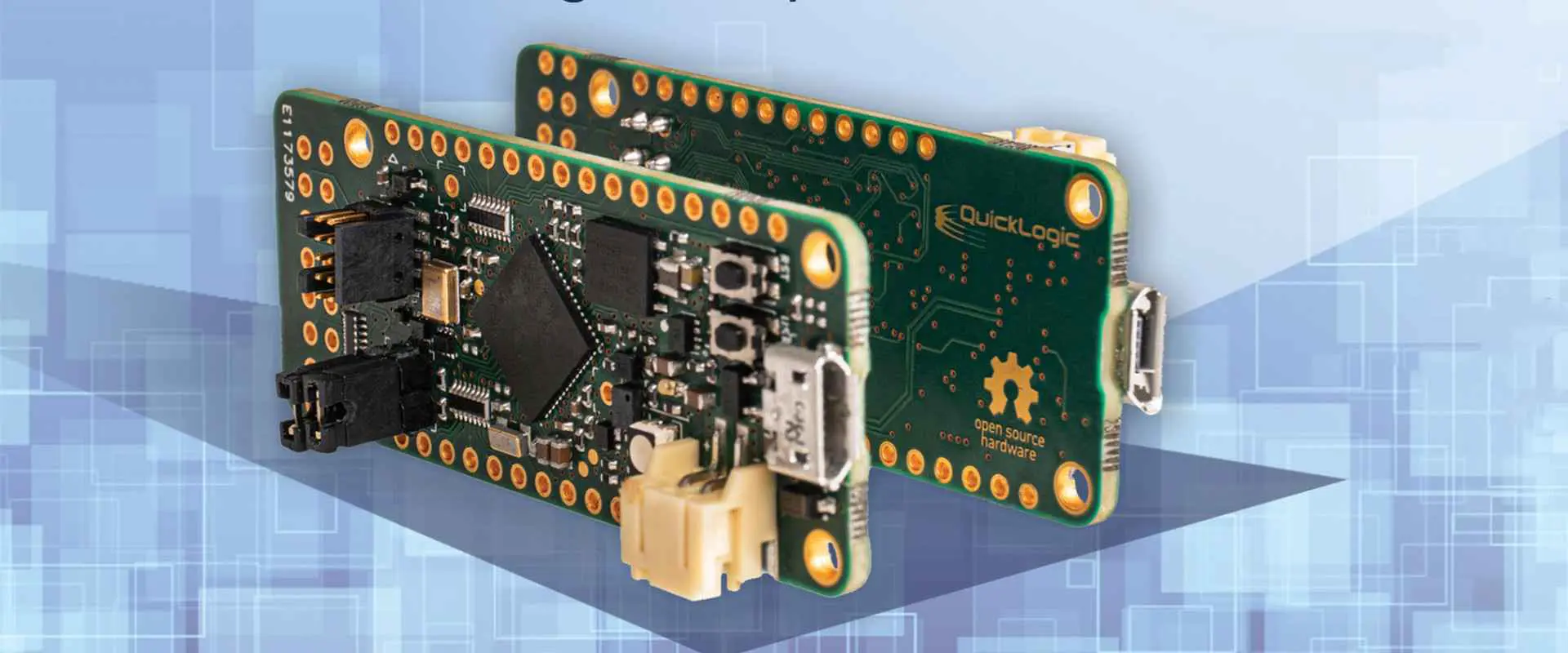
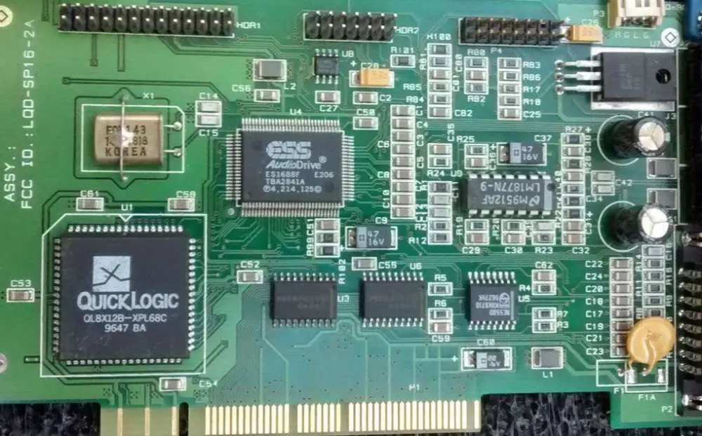
The current technology enables the world to be more connected than ever before. Therefore, specialized devices will become more critical as the world becomes more interconnected. In addition, we need tools that are easier to use and cost-effective. QuickLogic specializes in developing advanced logic devices for cutting-edge technology at an affordable price.
QuickLogic is proud to introduce the EclipsePlus family of products. It is a new range of logic device families for cutting-edge FPGA-based designs. They offer significant performance improvements over previous generations of technology. In addition, they have minimal increases in silicon area and power requirements.
The EclipsePlus family of products includes the EclipsePlus H8. It is a low-power 8-bit processor core with a 16-bit instruction word width and the 45nm EclipsePlus UV1. Additionally, it is a high-performance 1GHz+ ultra-low-power 45nm 8-bit processor core with a 16-bit instruction word width. The EclipsePlus family also includes an extensive range of peripheral IP blocks. In addition, it contains peripherals commonly found in ASICs such as ADCs, DACs, PLLs, and timers that we can mix and match to meet your needs.
The EclipsePlus family of devices has roots in the original Eclipse family of products developed by QuickLogic. The Eclipse family was initially a low-cost, low-power, high-performance 8-bit processor for general applications. They developed it originally for use in QuickLogic’s flagship ULE cores. However, it quickly became popular with other third-party manufacturers such as Rayming PCB & Assembly. As a result, they also included it in their design platforms, making it one of the most widely used 8-bit cores available today.
The next iteration of the Eclipse family emerged when QuickLogic began to look at ultra-low-power electronic device applications. Specifically, applications that required approximately 1mW and a 0.1V power supply. QuickLogic created a new generation of Eclipse devices based on the EclipsePlus architecture to meet these requirements. However, it has a much more aggressive power reduction methodology. Again, the goal was to fuse out the design rules for everything necessary for each specific product and make it ultra-low power.
To achieve this, QuickLogic had to make several changes from the previous versions of the Eclipse family. The most obvious modification was reducing the operating voltage from 2V down to 0.8V, reducing 33 percent in voltage. Also, to achieve the same performance as previous versions, QuickLogic had to increase the logic gates and reduce the number of registers. The result of these changes is a new ultra-low power. It was also a low-cost processor core with a low-cost FPGA supporting an impressive performance/power ratio. This is ideal for ultra-large area FPGAs. [Taken from QuickLogic product brochure]
The introduction of the EclipsePlus family represented a significant improvement over the prior generation. It was ideally suited for high-performance applications that required high density (such as large-area FPGAs) and ultra-low power applications that needed to consume less than 1mW.
The latest innovation of the EclipsePlus family
The introduction of the EclipsePlus family was an important stage in the evolution of QuickLogic products. Still, recent technology advancements and increased demand for high-performance devices forced QuickLogic to design a new generation of Eclipse products. The result is a new family called the EclipsePlus H8, a low-power 8-bit processor core with a 16-bit instruction word width. Its artful design can keep pace with Moore’s Law and take advantage of newer 45nm process technologies.
The EclipsePlus H8 implements some significant improvements over existing 8-bit cores that have been around since the 80s. For example, the decreased gate count, register complement, and power consumption. In addition, the EclipsePlus H8 features a 16-bit instruction word width, and the core can have from 32 to 128 registers. A special feature of the EclipsePlus H8 is that it supports register stacking. This allows access to multiple registers with a single instruction. In addition, the EclipsePlus H8 provides up to 1K memory locations for local variables stack and DSP math operations.
The EclipsePlus H8 has been suitable for use in both FPGAs and ASICs. However, both architectures require different sets of standards and specifications. QuickLogic developed a special design methodology to meet these requirements. It allows for implementing the EclipsePlus H8 in FPGAs and ASICs. In addition, this new methodology will enable designers to modify their designs from one architecture to the other easily. They will not need to rewrite the core logic or retest at a higher integration level.
The EclipsePlus H8 consists of an efficient logic design method called Logic Compaction. It came with the first generation of Eclipse products. This provided designers with a high-density design method for implementing 8-bit applications in the ULE FPGA2.
The EclipsePlus H8 core offers device manufacturers the ability to create high-performance, high-density FPGAs and ASICs that meet their customers increasing demand for larger quantities of more powerful devices. In addition, the EclipsePlus H8 provides designers with a cost-effective solution that they can use to implement not only high-level applications but also low-level embedded functions such as ultra low power monitoring and control devices.
2. Low power operation
The EclipsePlus UV1 core offers similar benefits to device manufacturers as the EclipsePlus H8 core. Still, instead of being used for high-performance applications, it has been designed for ultra-low power applications. It requires a maximum operating voltage of 0.6V.
3. EclipsePlus Design Methodology
The EclipsePlus design methodology offers device manufacturers a cost-effective solution for implementing high-performance, high-density FPGAs and ASICs at a fraction of the cost of other top-down methodologies. The EclipsePlus design methodology depends on a combination of super structured programming, logic compaction, and register stacking. It is programmable in VHDL, Verilog, and C, allowing designers to quickly and easily implement their designs in FPGAs and ASICs.
The devices that comprise the latest Eclipse family devices are below.
All members of the EclipsePlus family, except for the EclipsePlus UV1 core, offer embedded computational units (ECU) that can help implement various embedded functions. For example, ECUs provide integrated signal processing, DSP, and DMA functions. In addition, the ECUs include an on-chip memory that we can configure as a programmable memory bank.
2. Embedded Instruction Decoders (ED)
All members of the EclipsePlus family support embedded instruction decoders (ED). It helps reduce the size requirements of embedded applications. In addition, EDs accelerate high-speed execution in all significant microprocessors by allowing instructions to be fetched efficiently from off-chip memories. Thereby, it reduces the performance penalty caused by bringing instructions from on-integrated memories such as SRAM.
3. Advanced Clock Network
All members of the EclipsePlus family support a flexible clock network that we can configure to meet designers’ requirements. The clock network supports a FIFO-based counter, jitter, and input/output buffers. The clock network can also be helpful for direct interface with off-chip memories or peripheral devices.
key features include:
a) Four phase-locked loops: We use these to control peripherals such as external memory interfaces, serial ports, analog to digital converters, and counters. One is used to control the internal oscillator. The other three can be helpful for 3 different clock frequencies.
b) 16 I/O controls: These control the internal multiplexers and registers. Additionally, they control the interconnecting signals between the various units.
c) 20 quad-net networks: We use these to interconnect the various units. Generally, these contain either a FIFO or a counter to control data transfer between the CPU and other components.
d) Nine global clock networks: We use these to control the K, L, and M network, memory refresh, and special features such as the serial interface. One of the clocks is dedicated, while the others are available for higher-speed connections.
4. Programmable I/O
The members of the EclipsePlus family offer programmable input/output (I/O) units that provide designers with a flexible and cost-effective method for implementing custom I/O peripheral functions. The I/O unit consists of three outputs and two programmable FIFOs. The on-chip voltage regulator can control power dissipation.
Key features include:
a) High-performance enhanced I/O: These offer designers the ability to implement a wide range of I/O functions in low-power, high-performance packages. A single VDD line and two programmable sub-registers are helpful for control. We can configure each one independently to select any I/O port.
b) Programmable slew rate control: We can configure the slew rate to support AC or DC I/O connections.
c) On-chip voltage regulator: The regulator allows designers to power the I/O multiplexer and registers from 1.0 volt to 3.3 volts.
d) Three register configurations: These three programmable sub-registers can be configured to control the operation of the I/O. The first two are programmable independently, while we can configure the third as an output or input.
e) Eight independent I/O banks: Each programmable sub-register can control up to 8 I/O banks.
f) SSTL3, SSTL2, GTL+, PCI, LVCMOS, and LVTTL: The EclipsePlus family offers a wide selection of I/O standards. The LVCMOS, GTL+, SSTL2, and SSTL3 are available on the EclipsePlus UV1 core.
5. Embedded Dual-Port SRAM
The members of the EclipsePlus family offer embedded dual-port SRAMs that we can use to implement a wide range of memory applications. The dual-port SRAM consists of two banks, each of which has an independent address bus, a data bus, and input/output pins. The memory operates at speeds up to 167Mhz and has an on-chip voltage regulator that allows powering from 1.0 volt to 3.3 volts.
Key features include:
1) Configurable and cascadable: The memory configuration is programmable and cascadable. High-speed RAMs are supported, allowing users to configure up to 8MB of DRAM.
2) FIFO/ROM/ RAM wizard for automatic configuration: The EclipsePlus family of tools includes a RAM/ROM/FIFO wizard that automatically allows users to perform complex configuration tasks.
3) 82,900 RAM bits: Each one of the RAM banks has access to up to 82,900 bits. This is sufficient for up to eight banks of DRAM or up to 82,900 bits of ROM.
4) High-performance SRAM blocks: The number of SRAM bits available depends on the configuration. Bit sizes from 32 to 2,304 bits are supported.
The members of the EclipsePlus family offer programmable logic (PL) blocks we can use to implement a wide range of digital-specific functions. The PL blocks are based on standard low-power SRAMs and provide power dissipation from 1.0 volt to 3.3 volts.
EclipsePlus is used for programmable logic interfaces, enabling designers to implement custom electrical interfaces in a low-cost and high-performance package. Programmable interconnections between the external PL blocks represent a reduction in on-chip die area, and we can use it for custom timing cycles, control loops, and peripheral logic. Programmable input/output (I/O) is also available.
The programmable interconnections between the two PL blocks can implement numerous clock-based control loops, including clock recovery, filtering, equalization, and interconnecting signals. The interconnections also allow for data transfer between the two blocks. In addition to internal programmable logic, the EclipsePlus features lightning-fast response using on-chip FIFOs (and the lower power requirements of FIFO designs) as well as on-chip input/output buffers.
Key features include:
a) 347 I/O pins: Each PL has more than 350 I/O pins, allowing designers to create a wide range of devices. The number of I/O pins depends on the PL configuration and the RAM used for programmable logic.
b) 583,008 system gates: Each PL has a programmable gate configuration that we can use for standard logic functions, custom circuits, or logic blocks. The number of gates depends on the PL configuration.
c) 4,032 logic cells: Each PL can be a programmable logic cell configuration. The number of cells depends on the PL configuration.
d) 2.5 V VCC capable I/O: The I/O pins are capable of operating at either 2.5 volts or 3.3 volts, allowing them to interface with a wide variety of devices.
e) 0.25 µm five-layer metal CMOS process: The EclipsePlus can take full advantage of the superior performance of a five-layer metal CMOS process. As a result, the power dissipation is less than 45 mW at 167 MHz and can be reduced to 35 mW if needed.
f) Multi-path programming support: Designers can program different blocks based on the application requirements.
The EclipsePlus family includes several different software development platforms that support the complete range of member parts.
1. Third party
Third-party developers can customize any member of the EclipsePlus family. They can either develop their device drivers or software packages with the EclipsePlus.
The EclipsePlus is licensed to third parties as a complete package, providing a wide range of programmable logic functions, memory, and I/O interconnections. In addition, EclipsePlus’s features and a large number of configurable I/O pins make it an ideal platform for developing custom logic blocks.
The EclipsePlus hardware is also available to third parties as a supply source for customization and assembly of their own custom devices. This cost-effective solution allows loose coupling of the EclipsePlus design to unique needs.
2. Embedded designers
Software developers can use EclipsePlus features to develop their custom software components. The EclipsePlus provides a platform for developing custom digital-specific applications and reduces the cost of developing custom digital-specific products compared to FPGA devices. In addition, developers can translate their software into the appropriate PL configuration and create an EclipsePlus device using the EclipsePlus hardware with minimal changes to the developer’s code.
This is possible with all members of the EclipsePlus family, providing an open platform that allows third-party developers to customize programmable logic in a low-cost, high-performance package.
EclipsePlus programming environment
The EclipsePlus can develop custom logic elements rapidly using a familiar set of tools. After developers have created their software, a full range of options is available to configure their customized EclipsePluss. In addition to configuring internal programmable logic, external I/O level can be helpful, and the on-chip FIFO/ROM/RAM wizard can configure the configuration easily.
3. Designers with existing code
Developers can customize an existing design for use with an EclipsePluss. For example, they can create an EclipsePlus configuration to match the device they are developing or program their new customized device directly from their existing code.
The EclipsePlus is a family of products based on the same design. However, the devices differ in hardware configuration and features. The table below summarizes the features of all three current members of the family:
The EclipsePlus family has two significant sub-families: 1) a low-cost, high-performance PL solution designed for custom logic applications, and 2) an advanced PL solution designed to help design cost-effective FPGA digital specific components, supporting external memory and I/O interconnections, as well as fast clock recovery.
The EclipsePlus family of products is available through a wide range of distributors and directly from Quicklogic.
Quicklogic provides a fully digital design environment to support the EclipsePlus. In addition, the software development tools make digital design easier, faster, and more cost-effective by providing a standard set of tools. These tools include:
EclipsePlus designers can implement a wide range of devices with the same design flow for FPGAs, including custom logic blocks or custom digital-specific components such as VCOs, PLLs, SerDes elements, and complex components data converters.
The EclipsePlus design is available as free, open-source software. The EclipsePlus design file is available on the Quicklogic website. The source code files are also included in the distribution of the EclipsePlus design and provide a complete description of its architecture.
Quicklogic also publishes an EclipsePlus project on Github, providing a full description of each member part and its associated sources. FPGAs are widely used for complex digital applications such as high-performance image processing and video processing because they provide a wide range of programmable functions with low power consumption.
The EclipsePlus devices can meet the needs needed for design engineers, allowing them to implement very large systems at a low cost with high-performance capabilities.
Quicklogic is the only company that can offer a complete solution using an open-source design, software, and hardware.
The EclipsePlus Family is an open-source design that allows developers to customize a wide range of programmable logic elements and use them in FPGA design. The EclipsePlus devices depend on the same design used to manufacture the highly successful members of the Quicklogic family, providing advanced PL capabilities without the significant cost increase of development tools. In addition, the EclipsePlus can allow rapid implementation of custom digital-specific components at low cost and low power consumption by designers already familiar with FPGA designs for custom digital applications.
Installation
To install, first start the installation application:
1. Check the size of the EclipsePlus by clicking on the “Get File” button. This will download a file used to create a configuration file.
2. Open the “Eclipse-Plus-Firmware-[version]-BINARY-EN” (e.g., Eclipse-Plus-Firmware-1.2.2-BINARY-EN). If this is a .vhd file, copy it to a directory on your computer, then extract it using VC++ or some other C++ compiler generating tool.
3. Copy the “Eclipse-Plus-Firmware-1.2.2-BINARY-EN” file to the directory where you install your EclipsePlus, and rename it to “eclipseplus.hex”.
4. Open Upc_LcdxDriver_Win32 (EclipsePlus Projects) and select “run” from the top menu. The driver should then install automatically, displaying some messages about start-up and performing some initial configuration in your computer’s operating system for you.
5. If the driver does not install automatically, click “install” on the first screen of the driver, it will then run, and you must restart it whenever you want to open an EclipsePlus project.
6. Return to your EclipsePlus project directory and click on “open project” on the Upc_Lcd driver application that you see running on your computer’s desktop (or from a shortcut icon), giving an appropriate name in the open file dialogue box.
7. Your EclipsePlus should then start showing a blank screen for about two seconds before displaying whatever program you have written using the EclipsePlus controller (a typical program would require programming of various logic elements).
Developers can quickly and easily implement all the features of EclipsePlus digital designs, including all functions, inputs, and outputs of the design that are necessary for design engineers. The integration with an existing design using their existing code is also easily accomplished. Furthermore, many of the device settings are automatic, based on the model number of your device. The EclipsePlus uses a configuration file to determine basic settings such as clock frequency or power consumption which can be adjusted later if needed. Once the device is ready, you can download the controller application (which generates a lot of unnecessary code for no purpose) and use it with your system.
Suppose you have not already created a configuration file. In that case, you can create a copy of the generic configuration provided with the EclipsePlus design by clicking “Save as” in the “Save…” menu or by copying and pasting its contents into any file. This will set up all elements required to link your design using Device Manager in Eclipse. The configuration file contains all necessary settings during integration, including:
The programming model used is VHDL (a hardware description language). Using VHDL to program digital designs is the standard method in the industry and greatly simplifies the design flow.
Users then create a concrete VHDL file that describes all of the inputs and outputs of their system. This user-written VHDL part effectively replaces the “hardware description” part typically generated by FPGA tools. Next, we compile the resulting Once compiled. Finally, we execute the bitstream is held in memory and by the FPGA. Once the user has made some modifications to their design, they can then convert it back into a standard VHDL file that can configure the device with any FPGA tool.
Cost
The EclipsePlus design had low cost in mind. The design can operate on various FPGA devices using the same VHDL code. There are many different FPGA devices in widespread use, and the typical specifications of each device may be easily determined by looking them up in three sources:
A common distinction between FPGAs is their architecture. The EclipsePlus devices use an “abstract” architecture, allowing for much easier implementation on a wide variety of FPGAs that do not use the same layout.
The EclipsePlus can use a compact board layout and the fewest switches necessary. The framework can reduce unnecessary routing by providing a common framework for all the included functions, reinforcing the design philosophy. In addition, any unused components can be removed from their place on the board, leaving room for other items in a custom design. We implement the second iteration of each design on another bare circuit board (with the same basic dimensions) that uses the same wiring scheme as the main substrate but includes no extra parts.
This is useful if you use an existing board and do not want to move any significant components.
Conclusion
In conclusion, the EclipsePlus family can provide user-defined solutions for embedded applications. This supports advanced features such as programmable I/O, memory, SCSI, and serial ports. It is robust hardware that offers excellent performance. In addition, eclipsePlus family hardware is well-documented and free of patents.
The EclipsePlus core is the starting point for the entire design flow and is easy to use.
It can also be a stand-alone starting point and provides high performance and flexibility. The EclipsePlus core supports various peripherals such as I/O, memory, serial ports, and SCSI. In addition, a complete EclipsePlus board is available that supports these peripherals.
The semiconductor industry is a crucial part of the technology sector and the global economy. Semiconductors, also known as computer chips or integrated circuits (ICs), are essential components used in countless electronic devices we rely on every day. The semiconductor market was valued at over $500 billion in 2021 and is expected to grow steadily in the coming years.
In this article, we rank and profile the top 10 semiconductor companies in the world. Factors considered in developing the ranking include annual semiconductor revenue, market share, product portfolio, and impact on the industry. Understanding who the major players are provides insight into technology innovations and competitive dynamics in this vital sector.
Intel is the world’s largest semiconductor chip maker, supplying processors used in computers, servers, IoT devices, and other electronics. The company invented the x86 microprocessor architecture that became the de facto standard for PC processors. Intel has leading market share in CPU chips for PCs and data centers. The company is also expanding into other segments like AI, 5G, and autonomous driving.
Some key facts and figures about Intel:
Founded in 1968 and based in Santa Clara, California
Over 110,000 employees globally
Operates large manufacturing sites or “fabs” for chip production in the US, Ireland, Israel and China
Major brands include Intel Core, Celeron, Xeon and Atom processors
Holds over 17,500 patents and has R&D budget of nearly $14 billion
Samsung Electronics is a global leader in smartphones, consumer electronics, and semiconductors. It is the world’s largest memory chip maker with a dominant position in DRAM and NAND flash memory. The company is also a major player in logic chips and foundry manufacturing services.
Some key facts about Samsung’s semiconductor business:
Memory chips account for over 75% of Samsung’s semiconductor revenues
Operates the world’s largest semiconductor fabrication plant in Hwaseong, South Korea
Ranks second behind TSMC in global foundry market share
Major R&D and manufacturing facilities located in South Korea, USA, China, Japan
Investing heavily to expand capabilities in advanced logic chips and foundry services
3. Taiwan Semiconductor Manufacturing Company (TSMC)
Industry: Semiconductor foundry
Headquarters: Hsinchu, Taiwan
CEO: C.C. Wei
2021 Semiconductor Revenue: $56.8 billion
TSMC pioneered the dedicated semiconductor foundry business model when it launched in 1987. The company manufactures chips for fabless semiconductor firms using its advanced fabrication technologies and process nodes. TSMC is the world’s largest pure-play foundry and produces chips for leading companies like Apple, Qualcomm, AMD, Nvidia and MediaTek.
Key facts on TSMC’s foundry business:
Accounts for over 50% of worldwide foundry market share
Operates three advanced 5nm chip fabrication facilities
Major manufacturing centers in Taiwan, China, and the United States
Plans to invest $100 billion over three years in cutting edge capacity
Working on 3nm and 2nm fabrication technology ahead of competitors
4. SK Hynix
Industry: Semiconductors
Headquarters: Icheon, South Korea
CEO: Lee Seok-Hee
2021 Semiconductor Revenue: $36.8 billion
SK Hynix is a top memory semiconductor supplier behind Samsung. The company designs and manufactures DRAM, NAND flash memory, and multi-chip packages. Hynix memory chips are widely used in PCs, servers, mobile devices, and consumer electronics.
Key facts about SK Hynix:
Second largest DRAM memory chip supplier with over 20% market share
Mass producing 128-layer and 176-layer 4D NAND flash memory
Operates major fabs in South Korea and China
Also produces specialty foundry services for image sensors and display driver ICs
Plans to invest $97 billion in fab expansions and upgrades through 2025
5. Micron Technology
Industry: Semiconductors
Headquarters: Boise, ID
CEO: Sanjay Mehrotra
2021 Semiconductor Revenue: $27.7 billion
Micron is a leading memory and storage semiconductor company, best known for its DRAM and NAND flash memory chip products. The company focuses on advanced memory technologies for computing, networking, mobile, and embedded systems.
Key facts about Micron Technology:
One of largest global suppliers of DRAM and NAND flash memory
Manufactures memory chips at fabs located in the USA, Singapore, Japan, Taiwan, and China
Produces 3D XPoint memory technology jointly with Intel
Investing heavily in R&D for new memory innovations like GDDR6X and computectional memory
Acquired Intel’s noncontrolling stake in joint IM Flash fab sites in 2019
Broadcom is a diversified designer and developer of semiconductor and infrastructure software solutions. The company’s chip products support set-top boxes, broadband modems, enterprise storage, and industrial devices. Broadcom also provides networking, security, enterprise software, and mainframe computer solutions.
Some key information about Broadcom’s semiconductor business:
Leading supplier of chips for broadband, networking, storage, wireless communications, and industrial applications
Acquired Symantec’s enterprise security business in 2019
Purchased CA Technologies in 2018, expanding into infrastructure software
Operates wafer fabrication facilities in the US and Asia through its Broadcom Silicon Solutions division
Ranks among top five semiconductor vendors based on annual sales
7. Qualcomm
Industry: Semiconductors
Headquarters: San Diego, CA
CEO: Cristiano Amon
2021 Semiconductor Revenue: $27.1 billion
Qualcomm pioneered CDMA mobile communications technology and is now a leading fabless semiconductor company focused on wireless technologies. The company designs chips for mobile devices, wireless networking gear, automotive systems and IoT applications. Qualcomm’s Snapdragon processors power many Android smartphones.
Key Qualcomm semiconductor facts:
World’s largest supplier of mobile phone chips, including 5G chips
A major developer of 5G, Wi-Fi, Bluetooth and GPS standards
Produces application processors, modems, RF and power management ICs
Generates significant licensing revenue from its wireless patents portfolio
Outsources manufacturing to major Asian foundry partners like TSMC
8. Nvidia
Industry: Semiconductors
Headquarters: Santa Clara, CA
CEO: Jensen Huang
2021 Semiconductor Revenue: $26.9 billion
Nvidia pioneered GPU chips for advanced visual computing in PCs and data centers. The company now also develops platforms for AI, autonomous vehicles, high performance computing, virtual reality, and more. Nvidia’s graphics cards are top picks among PC gamers and cryptocurrency miners.
Key facts about Nvidia’s semiconductor business:
World leader in discrete graphics processing units (GPUs)
Produces mobile Tegra processors for smartphones and tablets
Acquired ARM in 2020, expanding reach into mobile computing
Investing heavily in R&D for innovations in AI, self-driving cars, robotics, and more
9. Texas Instruments
Industry: Semiconductors
Headquarters: Dallas, TX
CEO: Richard K. Templeton
2021 Semiconductor Revenue: $18.3 billion
Texas Instruments is a broad-based semiconductor company with a focus on analog chips and embedded processors. The company’s analog, logic, and wireless ICs are found in many electronic devices and everyday objects. TI also produces digital signal processors (DSPs) for audio, industrial, automotive, and other applications.
Some highlights of Texas Instruments’ semiconductor business:
World’s largest manufacturer of analog semiconductors
Operates wafer fabs in Texas, Maine, Japan, and China
Produces over 40,000 products including power management ICs, amplifiers, sensors, data converters, and calculators
Leading supplier of DSPs used in communications, automotive, industrial systems -analog chips account for over 80% of the company’s revenue
10. MediaTek
Industry: Semiconductors
Headquarters: Hsinchu, Taiwan
CEO: Rick Tsai
2021 Semiconductor Revenue: $17.6 billion
MediaTek is the world’s 4th largest fabless semiconductor company focused on wireless communications, HDTV, DVD and Blu-ray chips. The company’s chipset solutions power smartphones, tablets, smart TVs, Wi-Fi devices, Voice over IP (VoIP) and more.
Some key facts about MediaTek’s semiconductor business:
One of the top suppliers of ARM-based system-on-chip (SoC) solutions
Leader in 4G smartphone chipsets, expanding into 5G modem and RF chips
Strong positions in Chinese and Indian mobile device markets
Produces chips for smart home devices, voice assistants, Wi-Fi routers
Outsources manufacturing to foundry partners like TSMC and UMC
Ranking Methodology
The rankings were developed by analyzing the top semiconductor companies based on their annual semiconductor sales revenue. Additional factors like market share, product portfolio, and impact on the industry were also considered.
Publicly available information from company reports, industry reports, and financial databases were used to research and rank the companies. Only semiconductor pure-play companies or semiconductor business units were included in the ranking.
The following key criteria were used to select and rank the top 10 semiconductor companies:
Annual semiconductor revenue – Trailing 12 months revenue from sales of integrated circuits, wafers, and other semiconductor devices. This provides a direct comparison based on market size.
Market share – Percent share of the global semiconductor market across product categories like memories, microcomponents, sensors, analog ICs, discretes, logic, MPUs, MCUs etc. Firms with higher overall market share ranked higher.
Product portfolio – Breadth and strength of product line-up across semiconductors. Companies with diversified portfolios across multiple IC product categories ranked higher.
Industry impact – Reputation for semiconductor technology innovation and influence on the industry. Firms that drive more impact through R&D and new products ranked higher.
Fabrication capabilities – Possession of advanced wafer fabrication facilities, specialization in foundry services, and manufacturing capacity. This provides supply chain advantages.
Semiconductor Industry Overview
The semiconductor industry has shaped the digital age we live in today. Integrated circuits power technologies ranging from computers and smartphones to modern appliances, vehicles, medical devices and industrial equipment. Without semiconductors, most of the innovations in electronics over the last 70 years would not be possible.
Some key facts about the global semiconductor industry:
Total market size was $556 billion in 2021, projected to reach $1 trillion by 20301
Up 47% Year-over-Year compared to 2020 due to high demand and shortages2
Over 60 countries have semiconductor production capabilities
Asia-Pacific accounts for over 55% of global semiconductor sales3
The U.S. share of global semiconductor manufacturing capacity dropped from 37% in 1990 to 12% today4
The industry is characterized by constant technology advances and rapid obsolescence cycles
The semiconductor supply chain involves four major steps – design, fabrication, assembly, and testing. Key companies that drive the industry include:
Integrated device manufacturers (IDMs) – These firms handle the entire semiconductor manufacturing process in-house including design, fabrication, packaging and testing. Examples are Intel, Samsung, Micron.
Fabless semiconductor companies – They focus on IC design and outsource manufacturing. Qualcomm, Nvidia, Broadcom are leading fabless firms.
Foundries – These are standalone semiconductor fabrication plants that manufacture chips for other companies. TSMC, UMC, and GlobalFoundries are top foundries.
OSATs (outsourced semiconductor assembly and test) – Provide packaging, assembly and test services. Major OSATs are ASE Group, Amkor Technology, and JCET.
Applications of Semiconductor Devices
Semiconductors power technologies and devices in diverse end markets:
Medical Electronics – ICs for imaging, diagnostics, monitoring, implants, prosthetics, lab automation
Leading Semiconductor Companies by Revenue
Below is a summary table of the top 10 semiconductor companies ranked by their annual semiconductor revenue:
Rank
Company
2021 Semiconductor Revenue
Headquarters Location
1
Intel
$73.1 billion
Santa Clara, CA
2
Samsung Electronics
$58.1 billion
Suwon, South Korea
3
TSMC
$56.8 billion
Hsinchu, Taiwan
4
SK Hynix
$36.8 billion
Icheon, South Korea
5
Micron
$27.7 billion
Boise, ID
6
Broadcom
$27.5 billion
San Jose, CA
7
Qualcomm
$27.1 billion
San Diego, CA
8
Nvidia
$26.9 billion
Santa Clara, CA
9
Texas Instruments
$18.3 billion
Dallas, TX
10
MediaTek
$17.6 billion
Hsinchu, Taiwan
Major Semiconductor Industry Trends
The semiconductor industry is constantly evolving to enable faster, smaller, cheaper, and more power-efficient chips. Some of the major trends shaping the future of semiconductors include:
Miniaturization – Producing smaller transistors and denser chips by moving to advanced process nodes below 10nm and towards 3nm.
Heterogenous integration – Combining different chip architectures and specialties like logic, memory, analog, RF, sensors, MEMS etc. on the same package.
AI acceleration – Specialized AI chips and neuromorphic computing to provide huge performance gains on AI workloads.
Advanced packaging – Innovations like 2.5D/3D stacking to allow for greater integration and chiplet designs.
More sensors and embedded intelligence – Higher levels of sensing and decision-making abilities incorporated into devices.
Sustainability – Green manufacturing initiatives to reduce environmental footprint through renewable energy, recyclable packaging, lower emissions etc.
Outlook for the Semiconductor Industry
The semiconductor industry is expected to see continued growth in the long term driven by emerging technologies like 5G networks, Internet of Things (IoT), high performance computing, artificial intelligence (AI), augmented reality (AR)/virtual reality (VR), autonomous vehicles, cloud computing and more.
According to market research firm IC Insights, the semiconductor market is forecast to grow at a 9% CAGR between 2021-2025, reaching $778 billion by 20255. This growth will be led by memory and analog integrated circuits. Geographically, the Asia-Pacific region will remain the largest market, accounting for over 55% of semiconductor sales by 20255.
However, the industry could face some headwinds from geopolitical issues like the US-China trade war, Covid related supply chain disruptions, and chip shortages. Many governments are also announcing incentives and investments to boost domestic semiconductor manufacturing due to the risks highlighted by the chip shortage of 2020-2021. The industry will need to adapt to government interventions and changing trade policies.
Overall, the long-term growth drivers remain strong for semiconductors powering disruptive innovations across every industry. Chip companies will need to focus on advanced R&D and manufacturing scale to meet future demands.
Frequently Asked Questions
Q: Which country is the largest producer of semiconductors in the world?
A: Taiwan is currently the world’s largest semiconductor producing country, accounting for over 60% of total global wafer fabrication capacity. Within Taiwan, TSMC alone owns more than 50% of the worldwide semiconductor foundry market share. Other top semiconductor producing countries include South Korea, China, Japan, and the United States.
Q: What are the different types of semiconductor memory?
A: The main types of semiconductor memory chips include:
SRAM (Static Random Access Memory) – Fast, used for CPU cache memory
DRAM (Dynamic Random Access Memory) – High density, used for main computer memory
Flash Memory – Non-volatile, used for storage like SSDs and USB drives
ROM (Read Only Memory) – Stores
Top 7 US semiconductor companies
Are you someone who is looking for a job related to semiconductors and microelectronics? What about someone transitioning from working in the semiconductor sector or looking to expand their knowledge of this particular industry? Then, the Top 7 US semiconductor companies are right up your alley.
Corporations and consumers globally use semiconductors in many ways. Examples include computer circuit boards, jet engines, smartphones, and digital cameras.
A semiconductor is an electronic device that can amplify. It can also switch electronic signals or currents using conductive materials and insulators. These devices make up the core of all modern electronics technology. Semiconductors are also helpful in power plants. They can regulate the amount of electricity flowing into a system.
Semiconductor devices send and convert information in all modern technology. Semiconductor applications include cell phones, computers, televisions, digital cameras, and medical devices. The operating frequency of semiconductors is generally higher. We compare this to other electronic devices used in radios or speakers. As a result, they can also relay more information with reduced energy needs. Semiconductors use a small amount of power but can shift their frequencies fast.
When it comes to facts, the United States is the largest consumer of semiconductors in the world. The United States federal government and military are the largest purchasers of semiconductors. The Department of Defense is the largest single consumer in the United States. It accounts for about 30% of annual sales. The next two largest consumers are the high-tech and telecommunications industries. Those industries use semiconductors to design computers, networks, and cell phones.
The United States is the largest manufacturer and exporter of semiconductors. It has over $55 billion in annual sales. The single largest producer in the country is Intel Corporation. So, we refer to it as Intel. Other major producers are Texas Instruments Incorporated, Samsung Semiconductor, and Diodes Incorporated. About 35% of semiconductor production worldwide comes from the United States. The second-largest producer of semiconductors in Japan.
The percentage of American-made semiconductors exported abroad ranges from 10% to 20%. Many American semiconductor companies have factories in other countries. Some of these countries include Ireland and China. They do this to lower production costs and take advantage of cheap labor.
Intel sells over half of its annual production overseas. As a result, it makes it the most significant American exporter in the industry. For example, Sanmina-SCI Corporation has a large semiconductor factory in China. It is one of the world’s largest electronics manufacturing services (EMS) companies. The average wage at the Sanmina-SCI factory is $1.35 per hour compared to $25 per hour at Intel’s US factories.
Why choose US semiconductors
The United States has higher quality semiconductors than any other country. A study by the Semiconductor Industry Association revealed places in the US as the best. It shows that US-made semiconductors have a lower percentage of critical defects. The report states that defects in the US make up less than 1% of the total market. They also account for almost 5% of total sales in Japan.
1. Cost
Semiconductor manufacturing in the US is the most expensive in the world. This is according to a recent report by semiconductor market research firm Yole Développement. The report states that US-based companies must pay 50% more than any other country to manufacture semiconductors. Yet, despite higher costs, many companies manufacture semiconductors in the US. We relate this to better quality control and customer service.
2. Personnel
US chip manufacturers believe their employees have the highest quality workforce globally. Their employees are more experienced. They are also higher paid than employees in any other country. Employees at US companies also spend more time with customers. It allows them to provide more individualized customer service.
3. Quality of life
The SIA study revealed that workers at US semiconductors factories enjoy higher morale. Other country’s semiconductor workers report the contrary. This high morale results from a strong corporate culture. It allows employee input and identifies problems early on.
4. Support network
US semiconductor companies enjoy a strong support network with government agencies. They also have a great relationship with other trade groups. American chip manufacturers are lobbying the government to create better laws and regulations. Their primary issues are product safety, worker safety, and environmental protection.
6. Regulatory environment
America’s regulatory environment encourages investment in research and development. It also encourages private entrepreneurship in new technology industries. The report stated that the regulatory environment in the US encourages public and private investment. The partnership is in research and development. Also, it provides a competitive environment. It allows private entrepreneurs to create new technology industries.
7. Government funding
Government funding for new technology industries allows for government-sponsored investment. This investment provides scientists and engineers with funds. It helps chip manufacturers in the USA to create new products and technologies. For example, the SIA’s report stated that the US government spends billions of dollars through the Department of Energy. Also, they sponsor programs such as the Department of Defense (DARPA). Other departments include the National Science Foundation (NSF).
It is not easy to decide which US semiconductor companies are the largest. Some of the best include:
Intel corporation
The Intel Corporation was the first company to make a silicon computer chip. In 1975 Intel developed the first silicon chip. Such a move helped it to become a commercially viable process. Then, in 1984, Intel introduced its first 486 microprocessor. It was capable of over 4 MIPS (millions of instructions per second). By the end of 1995, Intel was producing more than 50 billion transistors a month.
The Intel corporation produces computer chips. We use them in all computers and other electronic equipment. For example, Intel’s PC chip is the most popular personal computer chip sold. Intel’s chips are also essential in satellite and cable television video games. Digital cameras and other consumer electronics products also use them.
The Intel corporation employs more than 100,000 people worldwide. Its plant in Arizona alone produces more than $50 billion worth of computer chips a year. They produce chips for IBM, Apple Computer, and Dell Computer. In 1999 Intel produced 45% of the world’s microprocessors for computers. It also produced over 95% for cell phones.
Applications:
Intel’s products are the basis for many computer systems. It includes those for the world’s largest supercomputers. Internet service providers and telecommunications companies also use its processors. Also, its chips power more than three-quarters of all notebook computers. It also powers about half of all computers manufactured today.
Innovation/Technology:
Intel Corporation is the leading innovator and manufacturer of silicon technologies. It is at the heart of all electronic devices, from cell phones to home computers. Intel’s global manufacturing and support network connect its customers to various products. They include software and technical support.
Global Market:
Intel Corporation’s brand and products are among the best in the industry. Also, the company has expanded its global operations, manufacturing, and marketing footprint. As a result, it helps them meet the growing demand for its innovative technologies.
Texas Instruments Incorporated (TI)
TI provides semiconductor and computer-related technologies and services. It offers memory, interface, analog, embedded processing, timing, sensing, and imaging products.
The company provides:
Microcontrollers
Operating systems software
Text display drivers
Evaluation boards
Software development tools
They also offer services that include
Design services for the semiconductor industry
Programmable logic device design support
Design services for the Web enablement of chipsets
software for embedded processing
This company started operation in 1951. It has its headquarters in Dallas, Texas.
Applications:
TI is the world’s third-largest seller of semiconductors. They are helpful in a wide variety of electrical devices. Their semiconductors are helpful in computers, telecommunication equipment, and other electronic products.
Demand/Supply:
TI is one of the largest employers in the Dallas-Fort Worth area. It reaches a peak of 7,000 employees during the busy season. The company also has an average annual revenue of over 10 billion dollars.
Innovation/Technology:
TI is one of the leaders in semiconductor technology. They have been the first to make several innovations. These innovations include their CMOS chip, a significant milestone in semiconductor technology.
Global Market:
TI is in Dallas, Texas. But on a global scale, it includes Germany, Singapore, and Japan. The company has a net worth of over 20 billion dollars. They rank number one in analog integrated circuits. Also, they are number three in microcontrollers in market share.
Nvidia Corporation is a global leader in processing graphics chips. It creates visual effects for modern video games. The company has built its reputation for creating high-performance graphics processing units (GPUs).
Nvidia Corporation started operating in 1993. It has its headquarter in Santa Clara, CA.
Applications:
Nvidia Corporation’s products are helpful in several industries, including computer, wireless, and telecommunications. The company’s products are also beneficial in several medical applications. The movie industry also uses Nvidia in its application. Nvidia also develops electronic design automation software.
Global Market:
Nvidia Corporation has offices worldwide and is a global company. As a result, they have expanded their reach to various countries. These countries include the United States, China, Japan, and India.
Innovation/Technology:
Nvidia Corporation is a leader in the technological industry. It releases many graphics processing units each year. Their products are essential for major companies like IBM, Sony, and Microsoft.
Demand/Supply:
Nvidia Corp has over 4,000 employees worldwide. Its revenue surpasses 1.5 billion dollars per year.
Micron Technology Inc. (MU)
Micron Technology Inc provides semiconductor solutions for products. They include DRAM, NAND flash memory, and NOR flash memory. They also offer system solutions to servers, personal computers, and mobile devices. Their products also include other peripheral components. An example is PCI Express cards that add graphics. They also have other features to computers, keyboards, hard drives, and solid-state drives.
Micron Technology Inc. (MU) started operating in 1978. It has its headquarters in Boise, ID.
Applications:
Micron Technology Inc. (MU) is a leading supplier of memory chips used in computer systems. Also, the company has expanded its reach to cover more markets. It includes mobile computing and automotive industries.
Demand/Supply:
Micron Technology Inc. (MU) has approximately 14,000 employees. It produces over one billion dollars of semiconductor products each year.
Innovation/Technology:
Micron Technology Inc. (MU) is one of the NAND flash memory industry leaders. The company releases various new products to meet the growing demand for memory chips. Also, the company is producing solid-state drives. These drives are applicable for mobile devices.
Global Market:
Micron Technology Inc. (MU) has offices and plants worldwide, including Taiwan, the West Bank, and Japan. The company’s market capitalization is at 3 billion dollars. They have more than 30,000 people across the globe.
Analog Devices, Inc.
Analog Devices, Inc. (ADI) designs and manufactures technology products and services. Some industries include computing, telecommunications, consumer, and automotive markets. The company offers integrated signal processing circuits. They process information from various sensors, communications protocols, and security systems. It also provides digital signal processors that generate radio frequency signals. These signals create television broadcasts and mobile phone networks.
Analog Devices, Inc. (ADI) started operation in 1965. It has its headquarters in Norwood, MA.
Applications:
Analog Devices, Inc. (ADI) is a leading manufacturer of high-performance integrated circuits. We use the most in industrial, computing, and communications markets. The company’s products are available to customers in over 50 countries worldwide.
Global Market:
ADI conducts operations worldwide. It generates over half of its revenue from outside the United States. It includes developed countries and emerging markets like China, India, and South Korea.
Innovation/Technology:
The company has invested in research and development for two decades. It is currently investing in new products to meet customer needs.
Demand/Supply:
Analog Devices is a global company. They have manufacturing facilities in North America, South America, Europe, and Asia. As a result, ADI has a global reach, and consumers from over 100 countries rely on its products. The company sells its products to companies that produce a variety of devices. They include televisions, GPS units, wireless phones, and medical devices. They also supply parts to the semiconductor industry. These parts include integrated circuits, image sensors, and accelerometers.
Microchip Technology (MCHP) is an IC supplier that has been in business for over three decades. The company designs and manufactures microcontrollers, fixed-function chips, and RFID systems. They also provide industry-standard solutions. It helps them to meet a variety of consumer and industrial applications.
MCHP started operations in 1969. It has its headquarters in Chandler, AZ.
Products:
Microcontrollers and Microprocessors, Analog, RFID, Static RAM
The company’s technology is helpful in various products. It includes automotive, communication systems, industrial, and personal computing. Also, Microchip Technology (MCHP) offers customizable solutions. These solutions allow customers to create custom designs for their applications.
Applications:
Microchip Technology (MCHP) is helpful in several consumers, industrial, and computing applications. The company works with various markets and consumers. They include medical, telecommunications, and entertainment products. Their technology is also helpful in several other products. For example, they have touch screen computers and hand-held barcode scanners.
Microchip Technology (MCHP) designs and manufactures a variety of chips. We use them in various applications. For example, it helps to improve the functionality and functionality of instruments and devices. Their products are essential in medical, wireless communications systems, and the retail industry. These devices include smartphones and digital cameras. They also supply software solutions for RFID tags. In addition, retailers use them to track inventory.
Global Market:
Microchip Technology (MCHP) has offices and facilities in over a dozen countries. They include the United States, China, Germany, India, and Japan. As a result, the company has a global reach to sell its products worldwide. Microchip Technology (MCHP) designs and manufactures technology products used throughout the global market. Their customers include some of the biggest companies in the world. Examples include Microsoft, Amazon, and Google.
Microchip Technology (MCHP) is a global company. It has manufacturing facilities in the United States, Asia, and Europe. The company’s products are available to customers in over 100 countries worldwide.
Innovation/Technology:
Microchip Technology (MCHP) designed and implemented new technology. We use them in wireless communications systems. The chip designs reduce wireless devices’ size and power consumption. At the same time, they also increase performance. The company is also working to create chips that will run on low power and remain energy efficient.
Demand/Supply:
Microchip Technology (MCHP) has several factories. They also have research facilities in Asia, Europe, and the United States. Also, their corporate offices are outside of the United States. Microchip Technology (MCHP) sells products to many companies. Most of these companies use mobile phones, mobile broadband devices, or GPS-enabled devices. The company’s customers include the US government and Fortune 500 companies. Also, various retail outlets and stores like Best Buy and Wal-Mart benefit from MCHP.
Xilinx designs and manufactures programmable logic devices. We use these devices in various consumer and industrial applications. These devices are application-specific integrated circuits (ASICs). We use them to develop consumer products and communications equipment. Xilinx started operating in 1984. It has its headquarters in San Jose, CA.
Xilinx develops programmable solutions for the consumer and industrial markets. They include medical devices, data storage, and communications networks. In addition, their technology is helpful in various products. They range from computer disk drives to smartphones and wireless networks.
Xilinx provides software tools, IP solutions, and services. They provide customers with everything they need to develop their integrated circuits.
Applications:
Xilinx has developed programmable solutions for various communications, imaging, and computing applications. Their technology is essential in several markets, including telecommunications, networking, and entertainment.
Xilinx designs programmable products in various industries, from gaming to health care. Also, their technology is helpful in various products, from mobile devices to computers. As a result, many consumers use Xilinx products daily without knowing it.
Xilinx has developed programmable logic devices for the communications industry. These products help improve the performance of many devices and applications.
Xilinx has several medical types of equipment, telecommunications systems, and computer networks. Also, these integrated circuits are essential in various entertainment systems. They include computers, mobile phones, and video game consoles.
Technology/Innovation:
Xilinx designs and manufactures integrated circuits used in various devices. Mobile phones, personal computers, digital cameras, and industrial control systems. The company markets these products to the interactive entertainment industry and telecommunications companies.
The Xilinx FPGA is an integrated circuit. It combines field-programmable gate array (FPGA) technology with programmable logic circuitry. The programmable functionality has a unique design. It fits into a single device configured to perform various functions for applications.
Xilinx also develops embedded system solutions, including storage and multimedia.
Demand/Supply:
Xilinx has offices and sales facilities all over the world. Major offices are in the United States, Asia, Europe, and Australia. A variety of customers uses the company’s products. They range from the mobile phone industry to the computer industry. All their customers rely on the company’s products. They use them to improve their products and create new ones for the market.
Xilinx has several sales and manufacturing facilities. Most of them are in the United States, Europe, and Asia. Their customers include a variety of industries. For example, they include the gaming, networking, communications, and telecommunications industries. Also, their customers include electronics manufacturers, telecommunications companies, and computer companies.
This consolidation will make these companies better prepared to compete against semiconductor companies. In addition, the growing research and development in China, Taiwan, and Japan are increasing competition. The semiconductor industry is one of the biggest industries in the world. It is also one of the fastest-growing industries.
China and Taiwan have been two leading nations in the semiconductor industry. They have been active for years now. We expect them to continue their dominance over the coming years. In addition, top players like Rayming PCB & Assembly boost growth in Asia.
The US’s main competitors in the semiconductor industry are Japan, Korea, and China. But, by 2023, we expect China and Taiwan’s global market share to be an estimated 25 percent each. It means that the US will only share 20 percent of the global semiconductor market.
As semiconductor companies grow, there is an increase in the demand for skilled labor. Also, there is a growing need for more engineers, scientists, and researchers in this field. Such is because of all the advancements made in technology and new products.
Conclusion
The semiconductor industry is one of the most rapidly growing industries globally. Over the last decade, there has been significant growth in demand for qualified workers. There is also a high demand for engineers to work in this field. Also, companies are using semiconductors to create new products.
We expect to see many more advancements. There will be developments made in semiconductor technology in the upcoming years. It will lead to more innovative products coming out of these companies.
When you see the term “X ray checking”, what comes to your mind? It is unbelievable for some designers that this term has to do with the Printed Circuit Board. If you are new to PCB designs, it is paramount you find out more about “What is X ray Checking?”
Interestingly, X ray is important in the world of PCB. This is primarily because it can penetrate every layer of your PCB so as aid inspection of the inner layers. Also, x ray checking helps with assembly of hard soldering of complex boards. In this article, you shall know everything you related to what x ray checking is about.
What is X ray Checking?
When it comes to soldering the PCB, you can’t ignore the important aspect of x ray checking. It really helps to inspect each layer of the PCB. This inspection needs to be carefully done.
Meanwhile, it is no doubt that across the globe, the circuit board inspection using the x ray is fast becoming more acceptable among engineers, designers, and PCB experts. However, this x ray technology is becoming faster and better every day.
Plus, X ray checking has to do with how well the layers of your circuit board can connect firmly. Hence, this x ray technology is an automated x ray system for inspection. Accordingly, this x ray checking helps to find out every unseen feature in your PCB.
However, do not forget in a hurry that x ray checking is not just limited to the world of technology. Also, in aerospace engineering, electronic manufacturing, and medicine we use this term. However, it may then have various meanings. For instance in medicine, the medics can carry out x ray to check some fractured bones in the body. Similarly, in the world of PCB, x ray checking helps to detect faults or errors during the manufacturing process of the PCB. Moreover, the x ray checking helps to test the quality of your circuit board. With this x ray technology, there are ways to avoid any damage on your PCB.
There are some underlying factors that affect how you inspect the layers of the PCB. These are listed below.
SMT
The Surface Mount Technology can affect the x ray checking of your device. The SMT affects how packages as well as leads become smaller. This way, it makes the circuit board have some density that is higher. As such, the PCB has some unseen components in its layers.
However with the higher density, the size decreases making the components of the circuit board become almost impossible for checking. The x ray checking then helps out to figure out each component of your PCB.
Component Size and Placement
The placement of each component of the circuit board influences the x ray checking. This implies that, when one is checking the component through the x ray technology, the size of each component determines how you inspect it. To save space, the devices are decreasing day by day making them more layered.
What are The Features of the X ray checking Devices?
For inspection of the layers of the PCB, there are ways the x ray checking works. However, the x ray checking devices have three simple features. Hence, they are listed below.
Platform
This has the ability to change the position of the samples in varying bearings or directions. This feature enables you to check your PCB from different angles. Also, this affects the magnitude from which you do the x ray checking of the circuit board.
X ray Tube
For anyone to have the ability to set up the x ray photons, you simply need the x ray tube. Plus, this is one of the features of the x ray checking devices.
Detector
This is an important feature of this device. It has the capacity to transform the photons into images. All it does is to sample various catches. Thereafter, it receives the x ray photons. Yet, it converts these into the required images. The heavier components consume more x ray photons. Wherefore, the lighter components are more translucent.
What are The Benefits of Using The X ray Checking Device?
There are benefits for inspection of the PCB using the x ray technology. Note that the metal is mostly dim for the images of the circuit board using the x ray technology. However, you see transparency when it is glass or ceramics. Then, it becomes so easy to view every metallic element.
This allows you to view different qualities of your circuit board. Also, you can know more about the varying problems that may arise. These include the following.
These occur during soldering. However, what causes it is as a result of the entrapping of gas which is mostly due to the water infection of the solder paste. Plus, the solder voids reduce the conductivity of heat at any solder joints. However, this can lead to any defect physically. Also, it decreases the possibility of readability. For you to identify this defect, you use the x ray checking device. So, you need to use it regularly.
Solder Bridges
These are problems you find common to PCB. However, the X ray Checking helps to easily find out about it. This defect occurs as a result of the closeness of your solder joints. However, this problem may not be easily known because other elements hide it. You cannot view it through optical checking. Only x ray checking helps you view it.
Conclusion
We believe now that everyone can understand that the x ray checking is important in the manufacturing of electrical devices. What is X ray Checking? It is simply the inspection of the layers of the components of your PCB. X ray checking helps to easily detect any defects which mere optical inspection can’t find out. Therefore, it is crucial you use this regularly during your assembly of the circuit board. It helps you easily detect the issues that may arise in future.
To know more about the topic, we need to know what the .STL Format is?A .STL format stored data about 3D models. it describes the geometry surface of a three-dimensional object. A computer-aided (CAD) program creates the .STL format. The .STL format is created as a final product of the 3D modeling process. It is the commonest format for 3D printing. Also, this format enables a computer to interact with 3D printer hardware when combined with a 3D slicer.
There are several CAD software packages that support the .STL format. Now, this format is widely used for several applications like computer-aided manufacturing and 3D printing. STL stands for stereolithography. Stereolithography is a file type designed by Chuck Hull in the 1980s.
What is the Difference between Binary and ASCII .STL Format
The .STL format offers two ways of storing data about the triangular facets. These two ways are the binary encoding and ASCII encoding. The two formats stores the data of each triangle as:
The components of the unit vector
The vertices’ coordinates
The Binary .STL Format
The .STL format uses the concept known as “tessellation” to encode information. Tessellation refers to tiling a surface with the use of geometric shapes in a way that no overlaps or gaps occur. If there are many small triangles in the tessellation, the ASCII .STL will be huge. Therefore, the binary .STL format helps to solve this issue. The binary .STL format is more compact.
Also, the header of this format begins with 80 characters. A 4-byte unsigned integer can help to indicate the total number of triangles. After this, there is information about the triangle. Each triangle is represented by twelve 32-bit floating-point numbers. Nine numbers represent the vertices’ coordinates. Also, the three numbers represent the 3D Cartesian coordinates.
ASCII .STL Format
This format offers details of the covering triangles. The ASCII .STL format begins with a mandatory line where <name> is the 3D model’s name. In this format, the vertices of the triangle are v1, v2, and v3. Also, a floating-point number represents coordinates values. This format ends with a mandatory line displayed as endsolid <name>
You can either choose the ASCII or binary format for exporting .STL format. Experts recommend the binary format for 3D printing. This is because it provides smaller file sizes. However, the ASCII is a preferred option if you need to manually inspect the .STL format for debugging. Also, the ASCII is very easy to read.
To 3D print .STL format, open the STL format in slicing software. This software is also referred to as a “slicer.” This 3D printing software transforms digital 3D models into printing instructions. Therefore, a 3D printer can create an object.
This software divides your STL file in hundreds of horizontal layers. However, this depends on the settings you select. The slicer calculates the amount of material needed by the printer to extrude. A G-code file entails this information. The settings of your slicer will affect the quality of your print. Therefore, it is crucial to have the appropriate software and work with the best settings.
The G-code is your 3D printer’s official language. Once your 3D printer features the G-code, it follows the instructions.
Pros and Cons of the.STL Format
The .STL format has several benefits. However, it has its own drawbacks. Therefore, it isn’t recommended for use all the time.
Pros
The .STL format is universal and almost all 3D printers support it. This makes it different from other formats like .3MF and .OBJ.
Most 3D printable models are in the .STL format. The combination of 3D printable models and STL-based software has increased the user base of this format. Therefore, there are many third-party software using .STL formats.
It is ideal for people who want to print with just one material or color.
Cons
The .STL format doesn’t have metadata like copyright and authorship details.
Also, this format can’t store additional details like material and color. It only stores data about the normal vector and vertices. Therefore, the .STL format isn’t an ideal option if you need to use several materials and colors.
There are several programs that help you to open and view .STL files.
Autodesk Viewer
This is a 3D modeling software that provides a professional-grade STL viewer. It is free. All you have to do is to create an account. After that, drop the file in your browser. Also, Autodesk Viewer comes with several advanced features. There are several tools for viewing. These tools include turning, panning, and zooming.
ViewSTL
This .STL viewer helps you to view 3D models online. Visit the website and drag your file. You will be able to view the .STL format in three different views. Also, ViewSTL supports other files like .3MF and .OBJ.
GLC-Player
GLC-Player has got a comprehensive set of features. Also, this online .STL format viewer supports many 3D file types like COLLADA and OFF format. Furthermore, GLC-Player comes with advanced viewing tools. With these tools, you can take snapshots and view cross-sections of 3D models. This .STL viewer has great rendering capability. Also, you can change the property of the camera to get a clear view from several angles.
Microsoft 3D viewer
Microsoft 3D viewer is a free online STL viewer that allows you to view 3D models. Also, you can view animations. This viewer supports common 3D formats. Also, it allows you to change the viewing and lighting modes.
MiniMagics
This .STL viewer is specifically designed for 3D printing. It helps to visualize 3D models. Also, it comes with basic features. These features include viewing parts by zoom, pan, and rotate. Also, you can get a cross-section view to check the interior tool.
JSCAD
This is a free STL file viewer that enables you to work both online and offline. However, JSCAD can only rotate around objects. Also, it offers an approach to develop and view 3D models.
Conclusion
We have discussed the .STL format and how it encodes information. Also, we reviewed programs that can help you view the .STL format. With this information, you would have more knowledge about .STL formats.
Amazingly, there are many benefits of using the Shengyi SG7350D PCB material for our designs. When you choose to use this PCB laminate with many outstanding features, your circuit board will last long. The reason being that it has a way of connecting every layer of your PCB board together. So, when you are assembling a circuit board with many layers, you can use this laminate because it is easy to design.
We shall ensure that we discuss in detail everything you need to know about the advantages of using the Shengyi SG7350D PCB material. Please, read through this interesting write-up to know more.
As outrightly stated above, there are many benefits of using this laminate for your circuit board. Apart from the fact that it makes fabricating the circuit board easier, it is very effective because of its high performance.
Easy to Design
When it comes to complexity, there are some PCB laminates that require only expertise to design. However, it is very simple to design Shengyi SG7350D PCB material. This is a type of laminate that every designer and engineer can easily design.
So, it doesn’t need only the professional designers and fabricators to design this laminate. Although there are simple steps required to design this laminate material. If you are not careful enough, you may miss out and not get the design right. This implies that you need to follow each step thoroughly when fabricating this laminate for your circuit board.
Laminate Strength
This is another importance of choosing this PCB laminate for your circuit board. Shengyi SG7350D retains its strength and stability no matter the exposure it may have to certain environmental conditioning.
Whether you expose it to high temperature, rain or sunshine, it is a very strong laminate material. However, you need to test its chemical reaction and mechanical strength when exposed to much force.
Plus, Shengyi SG7350D has very good peel strength, same as flexural strength. It is not the kind of laminate whose flexural strength weakens after a long period of time. Also, you need to give details on the way you prefer its strength when you are purchasing this from a designer or engineer.
Environmental Friendly
This is one advantage with Shengyi SG7350D. Shengyi SG7350D PCB material has a tendency to perform well in high temperatures. Yet, it retains its environmentally friendly property. This means, in no way does it cause any form of pollution after a long use.
Therefore, this is a type of laminate that uses materials that are safe for the environment. Accordingly, this is a lead free laminate. So, Shengyi SG7350D doesn’t contain toxic latex materials that are unhealthy for the environment.
Shengyi SG7350D PCB material and laminate allows for versatility during design. This laminate comes with various construction styles. This implies that there is no room for rigidity when designing. This is so because it uses varying materials for design.
Interestingly, the various glass weights allow the easy method for versatile construction. Also, you can design to your taste using various copper densities. Shengyi SG7350D allows creative thinking and innovative styles when constructing it.
Durability
Shengyi SG7350D is a highly durable laminate. Unarguably, it is one of the PCB laminates that can stand the test of time. There are so many factors that contribute to how long lasting this laminate material could be.
So, these factors include CAF resistance, weather resistance, and performance stability. It can withstand heat and no matter the density of water, it can last long. Therefore, this is a highly durable laminate for multilayer PCB.
Good Thermal Reliability
Of course, this is a key factor to consider when choosing any laminate material. Shengyi SG7350D PCB material has good thermal reliability as a feature. This means that it retains thermal stability under any temperature.
This laminate can work perfectly for PCB that one uses in a temperature that increases regularly. This means increasing temperature doesn’t have an adverse effect on this lead free material.
What Are The Features of Shengyi SG7305D PCB Material?
Notably, this is a feature of Shengyi SG7305D laminate. The thermal conductivity of this laminate material conducts amplified heat energy. So, proportionally the thermal conductivity of Shengyi SG7305D is enhanced. The transfer of heat rate of this PCB laminate material is high. Temperature gradient is in relation to thermal conductivity. As such, it is an important feature of Shengyi SG7305D.
Lead free Component
In addition, one feature of this laminate is its lead free material. It goes in line with any process that is lead free during construction. Interestingly, one can use Shengyi SG7305D for lead free applications. It is always suited for thermoset procedures.
Reliable Electrical Properties
The Shengyi SG7305D has reliable Electrical components. This is not the type of laminate whose electrical properties change after exposure to heat. Its electrical stability revolves around reliable electrical conductivity and dielectric strength.
Reinforced PTFE
Another feature of Shengyi SG7305D is its reinforced PTFE whose component is glass fiber. It has some amplified wear properties. This laminate material has high density and can resist any high or increasing temperature.
Therefore, this is why it is applicable for many industrial uses. Also, it makes it possible for versatile styles during construction.
This is one of the major areas where you can apply this PCB laminate. It helps to enhance the power magnitude of a power amplifier.
Signal Lamps
Also, you find this laminate in use for constructing signal lamps. It helps to improve the performance.
Conclusion
There are many benefits of choosing Shengyi SG7305D. Out of these numerous benefits, it is highly durable. This encompasses the fact that it is weather resistant. Also, this laminate is applicable in communication services. That is why you use it to improve the performance rate of these applications. No doubt, this laminate can withstand any degree of heat, same with water density.