Introduction
Surface mount technology (SMT) has become the predominant method of electronics assembly and PCB production for its efficiency and miniaturization capabilities. However, the complexity of SMT also introduces risks to product quality if proper control and oversight is not implemented. Defects introduced during SMT assembly can lead to immediate product failures or latent defects that emerge later in the field.
This article provides a comprehensive overview of critical quality assurance practices, testing procedures, metrics, and management strategies to guarantee high yields and reliability throughout the SMT production lifecycle. By instituting disciplined inspection, process controls, standards adherence, and continuous improvement, manufacturers can deliver robust and defect-free SMT assembly.
Design Stage Controls
Delivering quality SMT production begins in the design stages of product development:
DFA Analysis
Conduct design for assembly (DFA) analysis during board layout to identify any problematic areas for manufacturability and quality. Address issues like:
- Component spacing and density
- Placement sequence optimization
- Accessibility for inspection and rework
- Test point integration
Early DFA allows optimizing the design for ease of error-free SMT assembly.
Process Capability Assessment
Evaluate process capabilities against all design requirements during engineering prototyping. Verify the selected factory can achieve requirements like:
- Component sizes and pitches
- Solder joint sizes
- Component and board warpage control
- Placement precision
- Mixture of through-hole and SMT parts
Supplier Management
Qualify and control critical suppliers:
- Components – Require statistical controls and incoming inspection testing
- Solder paste – Validate performance through assembly trials
Controlling component and material quality prevents defects from cascade failures later on.
Quality Planning
Create a quality plan defining all inspection points, SPC metrics, standards, and controls to be implemented based on a design and process risk analysis. This roadmap guides manufacturing quality activities.
Incoming Quality Control
Rigorously controlling the quality of incoming parts and materials prevents defects from entering the production line:
Components
- Certificates of compliance – Review for acceptability from trusted distributors
- Sample inspections – Check component markings, lead forms, correctness
- X-ray inspection – Detect hidden issues like broken wire bonds
Solder Paste
- Mill/use by date tracking – First in first out (FIFO) usage
- Thawing/cooling logs – Monitor against specifications
- Paste viscosity tests – Confirm viscosity within limits
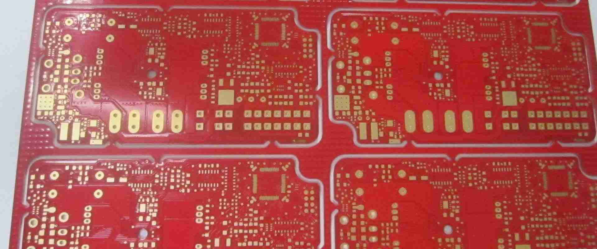
PCBs
- Netlist testing – Validate against approved data
- Visual inspection – Check for blemishes, scratches, missing markings
- AOI verification – Use automated optical inspection to catch board defects
Stencils/Tooling
- Dimensional checks – Verify to CAD models
- Microscopic inspection – Check for dents, debris, clogs
This prevents defective materials from reaching production lines and causing quality events.
SMT Production Process Controls
Rigorous process controls and oversight are critical during active SMT production:
Solder Paste Printing
Key controls:
- Vision alignment – Optically align PCB and stencil for accuracy
- Print parameter SPC – Monitor print speed, pressure, smear limits
- Stencil cleaning – Check and clean regularly for clogs
- Paste inspection – Volume, position checks, SPI monitoring
This achieves consistent, high quality solder paste deposition free of printing defects.
SMT Pick-and-Place
Robust process controls include:
- Feeder setup validation – Confirm right components in right feeders
- Nozzle inspection – Hourly checks for debris and wear
- Lighting and optics – Ensure calibrated and focused on PCBs
- Placement monitoring – SPC of speed, force, accuracy
- Component inspection – Regular SPI checks of centered placement
This minimizes misplacement and tombstoning errors during high speed component placement.
Solder Reflow
Key aspects to control:
- Oven profiling – Monitor temperature zones with thermocouples
- Conveyor speed – Keep consistent feed rate through oven
- Solderability validation – Verify parameter settings match solder paste
- AOI inspection – Automated post-reflow inspection of joints
- Thermal control – Measure and log profiles for each board
Controlling thermal profiles ensures evenly and properly formed solder joints.
Conformal Coating
For coated boards:
- Coating validation – Test coverage, cure confirmation
- Visual checks – Monitor coating quality, drips, unevenness
- Coating thickness – SPC measurements across boards
This reliably applies protective coatings against humidity and contaminants.
Automated Testing
End-of-line testing should include:
- ICT fixtures – Confirm test points make contact
- Continuity/shorts – Detect any open or shorted nets
- Functional test – Validate board operationally
- Boundary scan – Increased test coverage of components
Critical for identifying assembly defects before boards leave manufacturing.
First Article Inspections
Conducting comprehensive first article inspections validates process setup and capabilities for new designs:
- Perform dimensional inspection against CAD – confirm hardware matches plans
- Conduct visual inspection under magnification – detect any defects
- Run x-ray inspection – examine internal solder joint and wire bond quality
- Conduct ICT and functional testing – verify electrical performance
- Section and analyze solder joint cross-sections – validate process parameters
- Subject first articles to environmental stress screening – confirm robustness
First article approval establishes a known-good benchmark for judging quality as production ramps up. It also serves as process validation of product designs and CAD models.
In-Process Quality Monitoring
Ongoing inspection and metrics provide critical process feedback:
Statistical Process Control
Collect real-time production data like:
- Cpk values of print positions
- Pick-and-place accuracy
- Solder paste volumes
- Component rotations
- Solder joint dimensions
- Test yields
Chart control limits and monitor for trends or out-of-control points.
Process Audits
Frequently audit:
- Operator technique
- Program versions
- Equipment setup and maintenance
- Feeder setups
- Floor layout and material handling
Traceability
- Link products to production data through serial numbers and time stamps
- Isolate suspect lots quickly during quality events
SPC, auditing, and traceability provide rapid feedback for detecting issues.
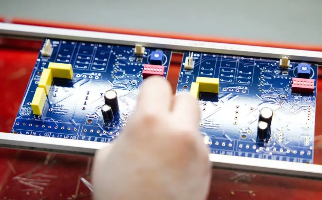
Automated Optical Inspection
Inline automated optical inspection (AOI) is indispensable for catching visual defects:
After Solder Paste Printing
- Detect missing, skewed, or incomplete print deposits
- Monitor print registration and offsets
After Component Placement
- Confirm presence and polarity of components
- Check for billboarding, tombstones, skew
- Inspect placement accuracy against CAD
After Solder Reflow
- Measure joint size, shape, and positioning
- Detect missing, insufficient, or bridging solder
- Find lifted leads, skewed parts, positional defects
Automated inspection improves detection rates and provides SPC metrics not achievable manually. Make use of available 2D and 3D AOI tools.
Failure Analysis and Defect Reduction
When defects occur, structured failure analysis and correction techniques are essential:
Defect Reporting
- Classify every defect by stage of occurrence
- Note process parameters involved
- Track by frequency, severity, project
Root Cause Analysis
- Leverage quality tools like 5 Whys and Fishbone diagrams
- Relate defects back to process variables with regression techniques
- Identify root cause patterns – training, machine wear, materials
Corrective Actions
- Address root causes – training, maintenance, materials, settings
- Standardize solutions into procedures
- Evaluate implementation and effectiveness
Analyzing defects improves processes for increased quality and reduced costs.
Qualification and Validation Testing
Testing protocols validate manufacturing processes and board quality:
HALT/HASS
Highly accelerated life testing reveals design weaknesses and defect risks. Stresses screening should include:
- Rapid thermal cycling (-40°C to 100°C)
- Vibration up to 60Hz across 3 axes
- Highly accelerated life testing up to 100G
This approximates years of field conditions over weeks to force latent defects.
IPC Validations
Use IPC testing standards like IPC-A-610 to validate quality:
- Soldering acceptance criteria
- Lead and terminal integrity
- Board assembly materials
- Cleanliness testing
- Cable and harness assembly
Certified IPC specialists can conduct testing and training.
Customer-Specific Qualification
Many industries have their own testing protocols:
- Automotive – AEC-Q000 and IPC-A-610 Automotive Addendum
- Aviation – RTCA DO-160 Environmental Conditions
- Military – MIL-STD-883 Component Qualification
Align with customer criteria through specific validations.
Qualification testing confirms designs, materials, and processes are ready for full production and field deployment.
Supplier and Subcontractor Management
Extensive supplier quality controls are essential:
- Maintain approved supplier lists – Block unapproved sources
- Require certificates of compliance – Mandate for all deliveries
- Conduct source inspections for high risk suppliers
- Enforce dock-to-stock quarantines until vetted
- Audit and score suppliers regularly – Take action on underperformers
- Provide clear specifications – Remove ambiguities
- Prevention over inspection – Require process controls from suppliers
Problematic suppliers can cease to exist. Control sources vigilantly.
Continuous Improvement Strategy
Steadily improving quality requires instilling a culture and mindset of continuous improvement.
Data Analysis
- Collect comprehensive metrics on rework, yield, defects, reliability field failures
- Analyze for patterns indicating chronic issues
- Prioritize worst pain points for correction
Idea Generation
- Empower production teams to suggest improvements
- Leverage programs like Kaizen and Lean to stimulate ideas
- Brainstorm solutions to longstanding problems
Implementation
- Standardize solutions into procedures and training
- Update documentation like work instructions and drawings
- Close the feedback loop by measuring impact
Continuous improvement delivers compounded gains over time.
Conclusion
Guaranteeing SMT quality and reliability requires extensive controls implemented in design, supplier management, process monitoring, inspection, testing, analysis, and culture. By rigorously verifying acceptability at each manufacturing stage, resolving defects through root cause analysis, and continuously improving processes, electronics manufacturers can assure their SMT production delivers premium quality and reliability. It takes diligence and buy-in at all levels, but the result is worth the effort for reduced costs and reputational gains.
Frequently Asked Questions
Q: What are the most common SMT defects?
A: Typical SMT defects include open solder joints, tombstoning, missing components, misalignments, bridging, billboarding, skew, solder balls, and insufficient solder. Tracking and analyzing defects points to corrective actions.
Q: How can you assess if PCBs are SMT-ready?
A: PCBs can be verified SMT-ready through netlist testing, inspection of soldermask and surface finish, and dimensional checks. IPC standards like IPC-6012D provide acceptance criteria.
Q: What are key solder paste controls?
A: Monitoring paste life, storage temperatures, stencil condition, and process parameters like print speed and pressure are critical for paste quality. Regular paste testing is also advised.
Q: What type of testing should be performed?
A: Testing should include ICT, boundary scan, functional testing, environmental stress screening, HALT/HASS, vibration, thermal cycling, and any customer specific industry protocols.
Q: How can you monitor hidden solder joint defects?
A: X-ray inspection and cross-section analysis are used to detect hidden voids, cracks, and other internal solder joint anomalies that can lead to field failures.
How to Find Low Cost SMT Production
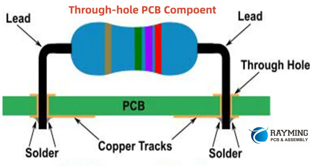
Do you have a need for SMT production? Are you in the food, electronics, or medical industry? Then, we can custom-design a production line to best suit your needs. Have you witnessed the dynamic changes in the synthesis of PCBs? Why are some PCBs quite different in design and dimensions? Nowadays, SMT has proven to be an efficient mounting style that minimizes the manufacturing cost. In the 1960s, assemblers developed this method, which later spread in the 1980s. Finally, in the 1990s, they used it in the leading assembly companies. SMT production has several advantages over the popular through-hole assembly technique, but at the same time, it has some demerits.
We are a leading provider of components and assemblies for the electronics industry. So whether you’re an OEM in need of bypass solutions or a hospital looking for fluid pump parts–we’ve got you covered! Our capabilities range from non-standard assembly items to prototype development and production.
What is SMT?
Surface mount technology (SMT) is a style we use while producing PCBs. It involves mounting electrical components on a bare board. SMT is a directly opposite process to through-hole mounting format. Assemblers developed it from the hybrid integrated circuit technology. SMT production is the process of synthesizing electronic circuits using plates or boards. In engineering literature, we refer to SMT as an SMT production line. We refer to electronic components prepared using SMT as surface-mounted devices (SMDs).
What are the steps in SMT production?
SMT is a lengthy process that requires a certain level of organization to achieve it. The following are the iterations that we follow in this production:
I. Component Preparation
Before proceeding to any other activity, we must prepare all the components and check for faults. For example, the bare board must have flat solder pads and no holes.
II. Stencil setting
We position the stencil according to the intended solder pad’s position on the PCB.
III. Printing of the solder paste
Solder paste, a mixture of tin and flux, works best in connecting the solder pads and SMC on the PCB.
IV. Placement of the components
The PCB moves on a conveyor belt to the pick-and-place machine, which places all the electronic components in their intended positions.
V. Reflow soldering
This process takes place in five consecutive zones. These are:
- Soldering oven – Having applied SMC, the boards continue to the reflow of the soldering oven.
- Pre-heat zone – This is a high-temperature zone with a temperature rising at one to two degrees Celsius per second until it is between 140ºC and 160ºC.
- Soak zone – the temperature in this zone is between140ºC and 160ºC. The boards spend between 60 and 90 seconds in this zone before proceeding to the reflow zone.
- Reflow zone – In this zone, the temperature rise rate is 1 – 2 degrees Celsius per second to a temperature between 210 ºC and 230 ºC. The tin in the paste melts, attaching the lead components to the pads. The surface tension of the molten solder aids in maintaining the position of the components.
- Cooling zone – As the board leaves the heating zone, they enter this zone which prevents abrupt cooling of the solder, hence eliminating connection problems.
VI. Cleaning and scanning of the board
Having soldered the board, we now clean them, checking them for any faults. We achieve this with the aid of flying probe testers, magnifying lenses, X-ray machines, and Automated Optical Inspection (AOI).
What factors do we consider when choosing the best SMT production machine?
The nature of the machine determines the quality and quantity of the products. It is therefore important that whenever you go for an SMT production machine, you consider the following factors:
The operating speed of the pick-and-place machine determines how many boards you can assemble within a given period. A machine with a higher speed will pick, inspect, and place more components within a short period. Therefore, it proves to be more effective in the mass production of PCBs.
A more accurate machine will perform numerous tasks without making many errors. Therefore, we are sure of high-quality products and maximum product outputs. In addition, the power consumption by the machine will be lesser if it has higher accuracy.
- Size of the components you intend to handle
If you purchase a surface mount technology machine, the size of the components you wish to mount using the machine is very important. Getting a machine that suits your components will save much of your time, as you do not need to go back to the dealer for machine exchange.
What are the advantages of surface mount technology (SMT) production?
- PCBs assembled using SMT are more compact and hence have higher circuit speeds.
- Using SMT, you can place many components closer together on one board. Eventually, you will have a smaller and more compact PCB with lesser weight.
- We can utilize both sides of the circuit board by applying SMT, allowing for more connections per component and a higher component density.
- SMT production process is, therefore, faster compared to the through-hole assembly since we do not require drilling holes on the bare board before the placement process. Thus, the preparation cost of the PCB will be lower.
- PCBs prepared using surface mount technology have lower inductance and resistance. Therefore, they will have higher frequency performance than those prepared with the through-hole assembly technique.
- Due to low lead inductance and compact package, the PCB will have an easily achievable Electromagnetic Compatibility (EMC).
What are the disadvantages of SMT production?
- The solder connections may get damaged as the PCB moves through different thermal cycles.
- Due to the less solder used in this process, the solder joints may not be reliable.
- Due to the small sizes, you will require expensive tools and a skilled operator to repair faulty PCBs.
- According to the design of the SMT-produced PCBs, we cannot install sockets that would facilitate the easy replacement of faulty components.
- SMDs are smaller in size than through-hole components, and therefore, there is no space for labeling the parts and stating component values.
- Subjecting components to mechanical strain may interfere with their functioning. Therefore, since SMT production involves stressing components to occupy smaller space, we cannot solely use it to manufacture PCBs.
Conclusion
SMT Production can help you take your business to the next level. Although SMT production is a highly specialized job and the demand for skilled SMT technicians will only increase, it is crucial to be on top of your game and have life skills you can use in any job.
We cannot perform SMT production successfully without an SMT production machine. If you want to purchase such a machine, the most suitable machine will depend on three factors. These are the speed, accuracy of the machine, and the size of components you wish to handle with this machine.