
RAYPCB · ENGINEERING GUIDE
Shengyi SAR10S PCB: IMS Dielectric and Thermal Planning
Shengyi SAR10S belongs to the aluminium-base insulated-metal-substrate material route. Its value in a PCB design comes from the relationship between copper, a thin insulating dielectric and the metal base. The dielectric must carry heat while maintaining the electrical isolation required by the product; thermal conductivity alone cannot select the construction.
This page focuses on that design tradeoff and the manufacturing information needed for an IMS inquiry. It does not assign a universal LED wattage or operating-voltage rating to SAR10S. Use the Shengyi material overview for the wider product family.
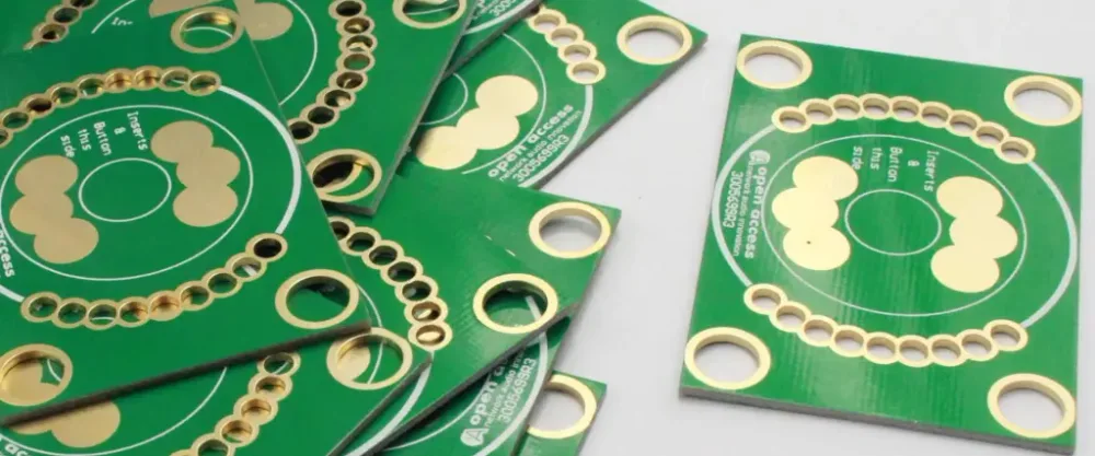
Draw the thermal path through the dielectric
For a simple one-dimensional model, thermal resistance is dielectric thickness divided by conductivity and heat-flow area. The metal base and copper may help spread heat, but they do not remove the insulating layer from the thermal path. A conductivity headline therefore needs a thickness and area before it becomes useful.
The official category consulted lists SAR10S at 1.1 W/(m·K). Confirm the method, direction and supplied revision before using that figure in a project model. The calculator deliberately starts empty; its example uses a hypothetical conductivity of 1 W/(m·K), not a preapproved material profile.
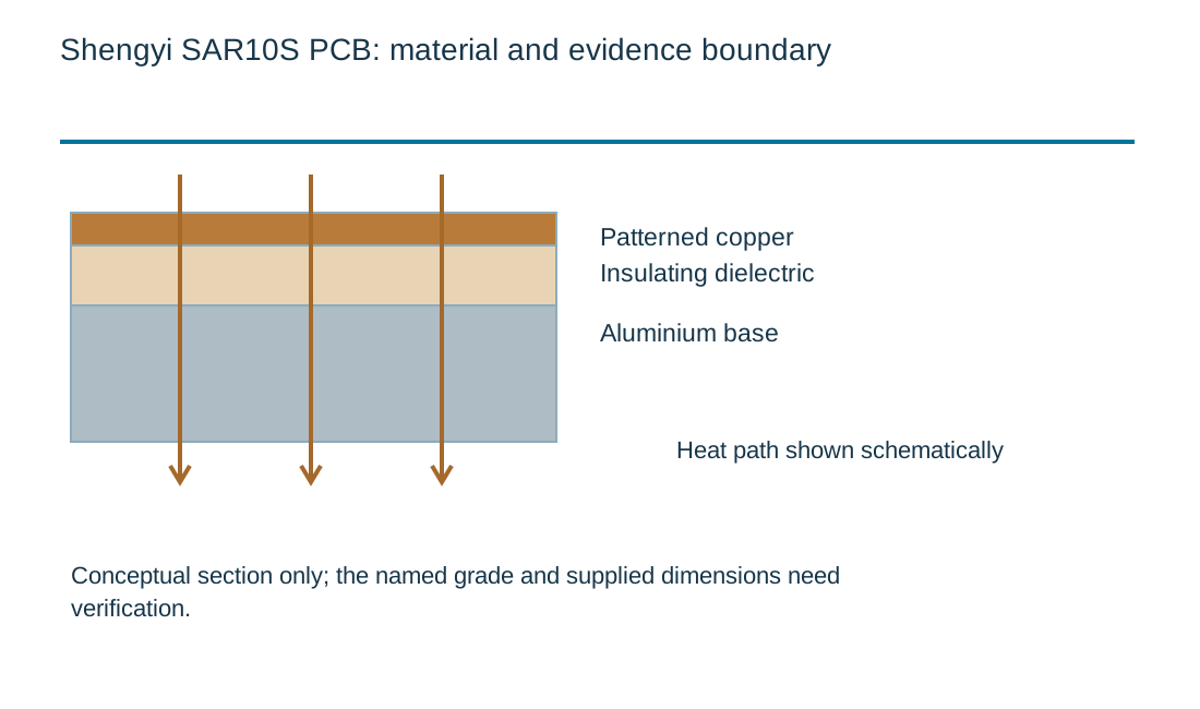
Source-qualified material review
| Item | Published information or evidence status | Design implication |
|---|---|---|
| Construction | Aluminium-base IMS with insulating dielectric | Thermal and electrical paths share the dielectric. |
| Conductivity listing | Official category lists 1.1 W/(m·K) | Confirm method, direction and supplied revision. |
| Calculation | R = t / (k × A) | One-dimensional dielectric resistance only. |
| Qualification | Project-specific electrical and thermal validation | No universal voltage or LED power rating. |
Work a thermal example with a clear boundary
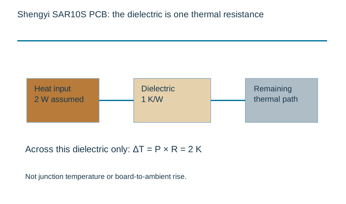
For 100 µm dielectric, 100 mm² uniform heat-flow area and conductivity of 1 W/(m·K), the ideal dielectric resistance is 1 K/W. Passing 2 W through that layer creates a 2 K temperature difference across it in the simplified model. The result does not predict LED junction temperature or board-to-ambient rise.
Interfaces, copper spreading, the aluminium base, mechanical contact and the heat sink add other parts of the thermal network. Small component pads may not use the whole board area uniformly. Treat the calculation as a boundary check, then use a more complete model or measurement for the assembled product.
| Review item | What to establish |
|---|---|
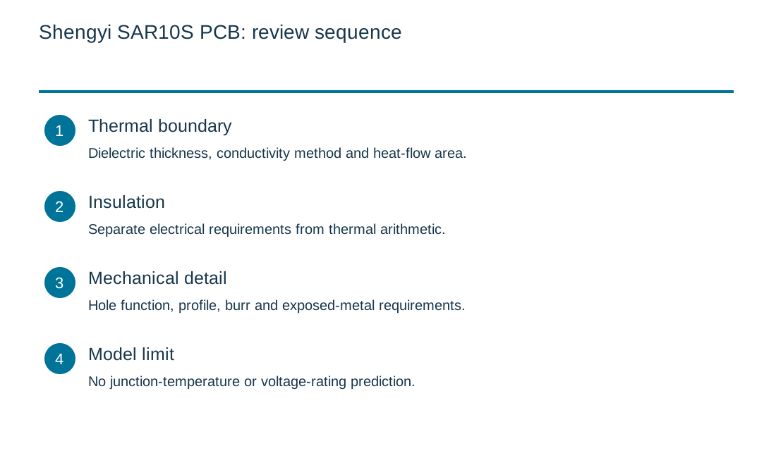
| Thermal boundary | Dielectric thickness, conductivity method and heat-flow area. |
| Insulation | Separate electrical requirements from thermal arithmetic. |
| Mechanical detail | Hole function, profile, burr and exposed-metal requirements. |
| Model limit | No junction-temperature or voltage-rating prediction. |
IMS dielectric thermal-resistance illustration
IMS dielectric thermal-resistance illustration
Use the current inputs and keep the assumptions
Start with the example only to inspect the units and the calculation boundary. Replace every assumption with a value tied to your own document or measurement. An empty numeric field is not zero. The review-reference field is a local label; avoid entering customer names, confidential part numbers or other private information into a public worksheet.
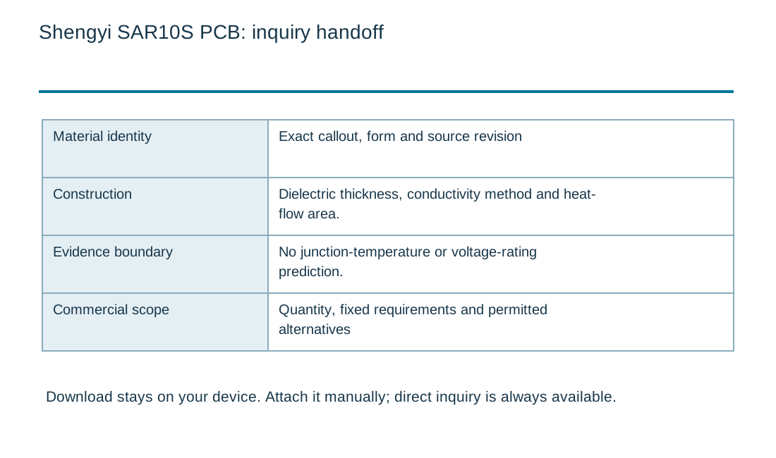
After calculating, read the notes alongside the numerical result. Changing any input invalidates the displayed result and disables its download until you calculate again. For a comparison, keep the units, geometry, material condition and measurement boundary consistent. A long decimal result does not imply equally precise input data. The downloadable record stays on your device and can be attached manually to an inquiry. It is not automatically transferred into the Contact form.
If an input is unknown, identify the person or document needed to resolve it. Do not fill a gap with a favorable generic value simply to obtain a result. You can request a material or fabrication review without using the tool. The arithmetic illustrates a relationship; it does not accept a construction, certify a material, establish current pricing or replace a supplier process specification.
| Input | What to establish before using it |
|---|---|
| Review reference | Nonconfidential revision label. |
| Dielectric thickness · µm | Actual insulating layer only, excluding copper and aluminium. |
| Through-thickness conductivity · W/(m·K) | Hypothetical value; replace with exact grade and method. |
| Uniform heat-flow area · mm² | Ideal common area through the insulating layer; no spreading. |
| Heat through this layer · W | Allocated steady heat flow, not total electrical input power. |
Optional cost comparison from your own allowances
Use a quotation or a clearly labeled internal assumption for each input. Keep the quantity, construction and inspection scope the same when comparing alternatives. This uncalibrated planning model adds entered values; it contains no current market rates and does not issue a RAYPCB quotation. You can contact the team without completing it.
Optional project allowance comparison
Preserve the electrical-isolation requirement
Thinner dielectric can reduce the modeled thermal resistance, but electrical insulation and manufacturing consistency still govern the permissible construction. State the working conditions, test requirement, conductor spacing and relevant equipment specification. Do not derive an allowable voltage from a thermal calculation.
Where tracking behavior is a primary concern, the S1151G high-CTI guide explains a different material question. CTI, dielectric breakdown and finished-board electrical testing are not interchangeable records. A metal-base design needs its own insulation and edge-clearance review.
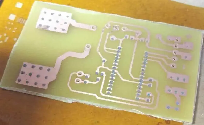
Review drilling, profiles and cleanliness
The supplier's IMS processing guidance should be read with the exact supplied construction. Holes and board edges can expose the relationship between copper, dielectric and metal. Burrs, contamination, damaged insulation and poorly defined clearances are practical concerns that a flat material property table does not show.
Provide the mechanical drawing, mounting-hole function and any exposed-metal or isolation requirement. Establish how the finished board will be inspected and electrically tested. Do not copy a generic FR-4 drill or routing recipe into an aluminium-base job without a reviewed process.
Compare construction choices instead of material slogans
A conventional laminate and an IMS board distribute heat differently. The CEM-1 callout review and CEM-3 construction review address reinforced composite substrates, not substitutes for SAR10S merely because they may appear in lighting products. Start with the thermal, electrical and mechanical requirements of the assembly.
For a cost comparison, hold board area, copper, quantity, finish, machining and test scope constant. Heat-sink interfaces and assembly support may affect the total product cost beyond the bare board. The optional worksheet adds your own allowances and contains no market price for SAR10S.
Send a thermal and mechanical inquiry together
Include component heat loads, the intended thermal path, board outline, hole drawing, copper, dielectric requirements, quantity and mounting arrangement. State which dimensions or insulation tests are fixed and which alternatives can be reviewed. If the temperature model is preliminary, label its assumptions rather than presenting it as test evidence.
An appropriate response should identify the proposed material construction and unresolved electrical or thermal questions. Keep the reviewed drawing and test requirements with the quotation. Availability, process capability and final performance must be confirmed for the actual design.
Review the entire thermal and insulation path
A laminate test, a finished-board qualification and an assembled-product validation address different boundaries. Preserve the specimen, conditioning, bias, temperature, geometry and observation interval with every result. A favorable value at one boundary cannot silently become approval of the whole product.
Separate a declaration of restricted substances from process compatibility and from service reliability. Keep customer-specific requirements and change-control obligations explicit. When a grade or construction changes, identify which evidence remains applicable and which work must be repeated.
For a manufacturing inquiry, provide the mission conditions, controlled drawings, material requirements and requested records. Mark unresolved qualification items as open. The worksheet can help organize evidence or compare a physical relationship, but it cannot certify compliance, predict lifetime or assign a universal safe operating limit.
An insulated metal substrate is part of a thermal system, not a standalone temperature rating. Identify where heat enters the copper, passes through the dielectric and reaches the metal base, interface and heat sink. The steady one-dimensional model on this page covers only the entered dielectric layer and uniform area.
Electrical insulation remains a separate requirement even when reducing thermal resistance is the main objective. Thickness, local defects, edges, holes and contamination can matter to the finished construction. Define the actual electrical test and equipment requirement rather than inferring an operating voltage from a material conductivity value.
Mechanical details can change both paths. Mounting pressure, flatness, interface material and exposed-metal regions affect the assembly, while drilling and profiling require appropriate controls. Provide the relevant mechanical drawing and identify which surfaces or edges have functional requirements.
For procurement, compare the complete deliverable. A bare-board price does not include every heat-sink, assembly or verification cost. Keep the proposed material, insulation evidence, thermal assumptions and test scope in the quotation so that an apparently lower-cost option is assessed against the same functional boundary.
Standards, source context and limits
Use the edition, amendment and material-document revision named in the purchase agreement. A standards title, marketing label or supplier product family does not establish that a particular lot meets a requirement. Public summaries are useful for scope; the controlled specification and applicable test method govern acceptance.
The examples on this page are illustrative engineering scenarios. They are not RAYPCB production records or guaranteed material values. Source links identify the organizations responsible for the referenced information. Confirm applicability to the exact grade, construction and test condition before carrying a number into a drawing or qualification report. Sources were reviewed on 3 October 2026. A public catalog search is not proof that an unlisted product never existed. Where the exact designation or current technical sheet could not be verified, this page provides a clarification workflow rather than an invented material specification. Current supply, construction availability and qualification remain separate questions.
For fabrication scope and the agreed construction requirements, see PCB manufacturing.