Characteristics and benefits of HUBER+SUHNER RF Components

RF Components

RF passive components are helpful in the transmission of electromagnetic energy. As a result, these components are useful in various applications and platforms. For example, they are necessary for aircraft for flight tests and telemetry applications, missile experiments, data link communications, robots, and electronic warfare systems. They are also ideal for wireless communications between aircraft.

We can use RF passive components in wireless communication base stations and indoor distribution systems. These systems provide continuous coverage of wireless signals indoors by splitting the signal from a base station. To achieve this, we distribute the signal to the antennas of coverage points. The antennas of the coverage points then receive the signal, achieving continuous indoor coverage.

Passive components can control the flow of energy in a circuit. In contrast, active components are devices that produce electrical signals. These devices include transistors, silicon-controlled rectifiers, and diodes. Active components require an external power source to function. On the other hand, passive components influence the flow of power without requiring an external power source.

The RF Unit

An RF unit is a device that emits radio frequency waves. These devices are commonly in power lines and streetlights. There are several ways to protect yourself from this radiation. One way is to de-energize the RF unit and then work around it. Another way is to maintain a safe distance.

Another form of RF unit is a mobile device. These devices can move from location to location. They are often suitable for use with at least 20 cm separation from the transmitter and the user’s body. Some examples of mobile devices include smartphones and tablet computers. These devices can connect with other devices.

RF components are also helpful in televisions and media players. These devices use RF modulators to change the signals they receive. These devices can change audio and video signals from any source. This way, you can control how much output you get. Sometimes, you can control how much power your television can handle.

The FCC regulates RF components. They are classified based on their components and devices and are subject to different rules. Therefore, you can incorporate an RF module that meets the applicable requirements to avoid violating FCC rules.

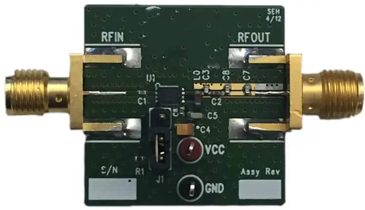
The RF Circuit in low noise amplifier

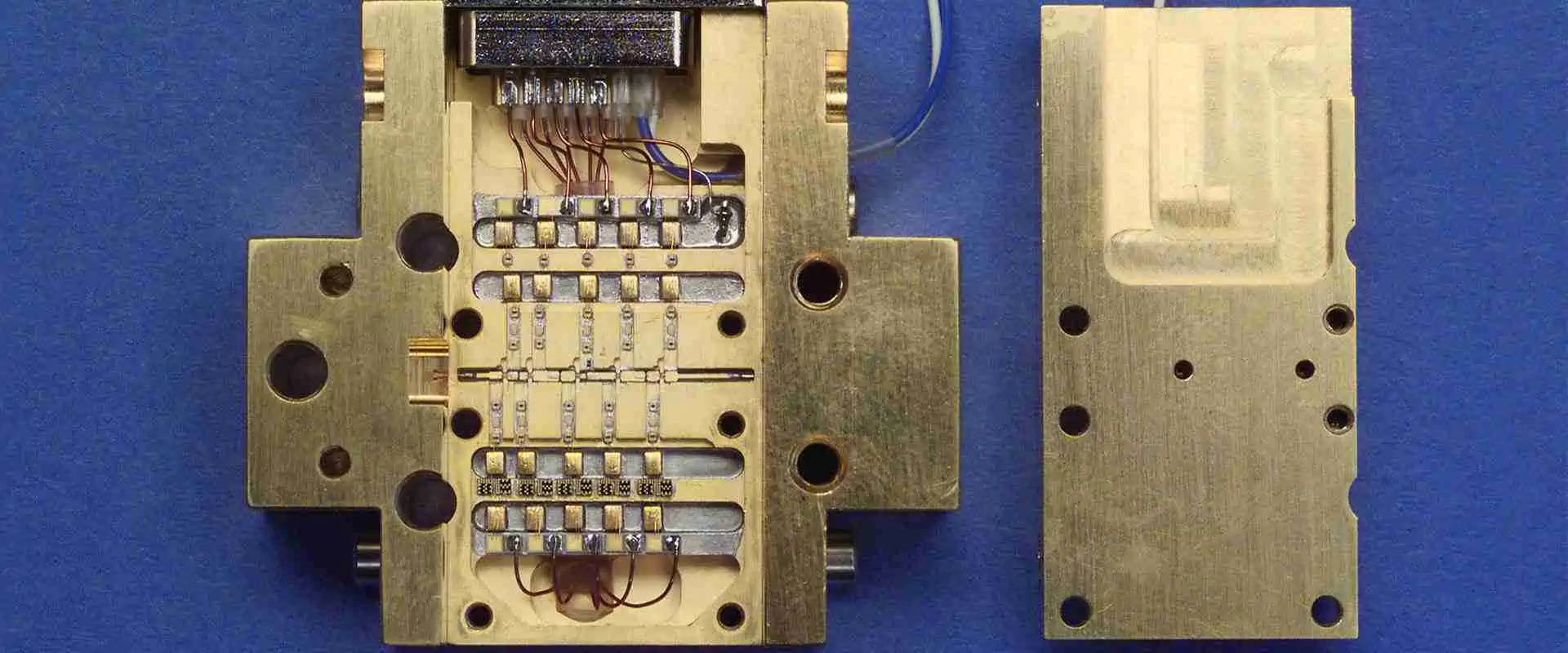
An RF circuit is an electronic device that uses radio waves to transmit information. It is highly sensitive to noise, such as voltage glitches. To reduce the chance of failure, one should design it so that it can withstand voltage glitches and still perform its function. For this reason, it is essential to place decoupling capacitors strategically. For example, if a circuit contains an IC component, it should have two decoupling capacitors placed in parallel with the component.

RF PCBs are becoming increasingly popular in mobile phones and cellular networks. As a result, they have evolved from simple thick copper-clad boards to multilayer PCB that can handle higher frequencies. These multilayered boards are made of thin copper layers and are incredibly flexible. This makes them easy to integrate into mobile devices and other space-constrained equipment.

An RF circuit is a complex device that uses active devices to adjust signal frequencies. It includes various components, low and high-power amplifiers, modulators, and demodulators. An amplifier increases the voltage of an RF signal, typically to a few millionths of a volt, while a modulator alters the RF carrier’s frequency. A demodulator, on the other hand, extracts information from the modulated carrier.

RF Circuit Design

RF design involves the placement of decoupling capacitors. The simplest circuit has two decoupling capacitors placed in parallel with an IC component. Each capacitor should be on the same layer as the other. The decoupling capacitors should also have individual ground vias. In addition, they should be in ascending order of their capacitance from the power supply. This means that the lower capacitance capacitor should be closest to the power supply.

RF componenets operate at high frequencies and high power levels. With higher frequencies, these constraints become even more critical. In addition, the reactance of the signal traces becomes increasingly essential. As a result, microwave circuits require much more power than a conventional circuit can handle. The physical layout of the circuit must account for this.

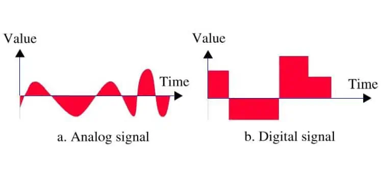
RF circuits are ideal in many applications, but wireless communication is one of the most popular. The block diagram in figure a shows a typical wireless communication system. Figure A shows the receiver and transmitter circuits. It also shows the digital processing part that processes the digital signal.

Types of Active radio frequency Components in Circuits

There are two basic types of active components: voltage-controlled devices (VDS) and current-controlled devices (BJTs). Voltage-controlled devices operate by supplying energy to a circuit whenever the current leaves the positive terminal. Current-controlled devices are constant, nonvolatile sources of current which control the flow of charge in the circuit.

On the other hand, passive components cannot control the flow of electricity, although they can store energy, produce an inductance, and resist the electric current. Both types of active components are commonly used in every electronic device and have a variety of applications. Some active components include computing power, built-in batteries, and LED lights.

Active components, which include diodes and integrated circuits, can be used in RF circuits. They are also helpful in other circuits, such as analog and low-frequency digital circuits. However, RF circuits are different because their designs require different objectives and challenges. They may also use integrated circuits that perform functionality unique to RF systems. In addition, they may be unfamiliar to designers unless they’ve worked with RF circuits for a long time.

The two main types of RF circuits include power amplifiers and low-noise amplifiers. A power amplifier provides power and a low noise figure, while a low-noise amplifier provides a high voltage gain and low noise figure. In addition, both RF circuits typically include a mixer that mixes two signals: the transmitter mixer and the receiver mixer. Finally, a filter controls the signal energy and is essential for preventing cross-talk between radio signals.

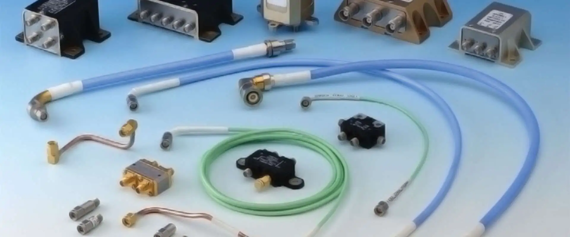
HUBER+SUHNER Components

FULL PCB MANUFACTURING Quote

HUBER+SUHNER is a company that develops and manufactures radio frequency and microwave components. Their products include Broadband directional couplers, Fixed attenuators, and RF-over-Fiber modules. They are also certified by ISO 14001, TS 16949, IRIS, and EN(AS) 9100.

HUBER+SUHNER develops and manufactures radio frequency and microwave components

HUBER+SUHNER is a Swiss-based company that develops and manufactures components for optical and electrical connectivity. The company’s products serve the Communications, Transportation, and Industrial markets.

The company’s product range covers various technologies, including optical and radio frequency. The company focuses on delivering high-quality, high-reliability products to global markets. The company has subsidiaries in over 80 countries. HUBER+SUHNER’s expertise lies in its extensive knowledge of radio frequency synthesizer, state-of-the-art test methods, and comprehensive understanding of surface coating.

Broadband directional couplers

The HUBER+SUHNER Broadband Directional Coupler portfolio provides broadband directional couplers for indoor applications. They support frequency ranges from 380 to 2700 MHz. They also provide the flexibility to use multi-band antennas and wireless base stations. Available with N or G interfaces, they can minimize signal degradation.

HUBER+SUHNER Broadband Directional Couplers are typically essential for use with industrial wireless communications systems. They can be mounted directly to access points or cabinets. They are also suitable for installation on building walls. Their design flexibility makes them suitable for a broad range of applications.

Fixed attenuators

HUBER+SUHNER specializes in the development and manufacturing of electrical and optical components for a variety of applications. Their extensive knowledge of radio frequency technologies and state-of-the-art test methods help them develop components with superior performance and minimal impact on signal quality. The company also designs custom designs for specific applications.

RF attenuators are used in communication and test & measurement applications to decrease the power of a transmitted signal without distortion. They are available in fixed and adjustable versions. In addition, they are used to improve the impedance matching between subsystems and to protect test equipment.

RF-over-Fiber modules

RF-over-Fiber modules from Huuber+Suhner combine radio frequency components with fiber optic technology to provide bidirectional communication over a single channel. The modules can be used for various communications applications, from defense systems to test environments. In addition, they offer a small footprint and are ideal for harsh environments.

The company’s RF-over-Fiber modules can meet the demands of industrial, transportation, and communication markets. They combine low-frequency technology with high-performance, long-life, and quality components. HUBER+SUHNER is headquartered in Germany but has subsidiaries in more than 80 countries worldwide.

The growing RF-over-Fiber market is due to the increasing use of smart devices, high-speed internet, and mobile users. This technology provides a future-proof connectivity platform. In addition to RF-over-Fiber modules, HUBER+SUHNER also offers optical switches and DE multiplexer modules. The growth of this market will continue over the coming years as the use of RF-over-Fiber solutions continues to increase.

RF subminiature connectors

HUBER+SUHNER has a large selection of RF subminiature connectors. These connectors have excellent performance and size-weight balance. In addition, they are available in various connector types. We test them according to CECC 22220, an international standard for micro coaxial connectors. While these connectors are similar in basic design, the coupling mechanisms and frequency range vary slightly.

Huber+Sohner is a global leader in radio frequency components and has many years of experience in the engineering of coaxial connectors. In addition to a wide range of standard connectors, the company also manufactures customized connectors, cable assemblies, and integrated assemblies.

Advantages of a HUBER+SUHNER DC Block

RF PCB Manufacturer
RF PCB Manufacturer

A DC block is a device that separates DC voltage from RF frequency. Its function is to protect devices from being damaged by DC voltage. This product is available from over 60 manufacturers. Its advantages include excellent quality, reliability, and long service life.

A DC block is a high-pass filter to keep direct current (DC) from flowing through a transmission line. Because DC voltages have a frequency of zero Hertz, they can interfere with sensitive RF components. DC blocks consist of capacitors placed in series with the transmission line. They prevent the flow of DC energy while still allowing RF signals to pass through with very little attenuation.

Why Advanced Technologies Have the Best RF Devices

RF components are a key part of modern electronics. They allow for higher levels of integration, security, and flexibility. However, many of these devices still rely on cell towers, which can become overloaded during an emergency situation and result in poor reception. This is a significant issue for healthcare, manufacturing, and public safety teams, who must remain connected.

RF technology is a critical component of modern electronics

The latest RF components are available on the market. They offer the most advanced performance, allowing users to communicate with other devices easily. These technologies are also very cost-effective, enabling thousands of devices to connect. They also have a frequency range of 15 kilometers, which is ideal for large-scale Internet of Things applications.

RF components are suitable for various applications, ranging from telecommunications to consumer products. In addition to providing radio frequency energy for these purposes, they also have other uses, such as producing mechanical vibrations or accelerating charged particles. RF components fall under the jurisdiction of the FCC and must comply with specific rules and regulations. Examples of such products include fluorescent lighting, halogen ballasts, arc welders, microwave ovens, and medical diathermy machines.

Today’s wireless devices also need to support multiple standards. Wi-Fi standards have become increasingly complex, with RF components requiring higher frequencies. For example, Wi-Fi 6E and 7 enable high throughput and low latency, but their higher frequencies require complex modulation schemes and system co-design. To meet the requirements of these standards, manufacturers can use Qualcomm ultraBAW filters to optimize performance.

RF semiconductors offer higher levels of integration

The demand for more compact handsets has led to higher integration levels in the handset RF semiconductor industry. To keep up with the increasing demand, suppliers have shifted their focus from traditional integration techniques to modular design and development of complete radio solutions. These developments have spurred the development of more advanced RF semiconductor devices for handsets, increasing the dollar value of these RF devices. As a result, RF semiconductor designers must constantly upgrade their designs and migrate to new process technologies and updated manufacturing techniques to keep up with this trend.

The cost of developing RF components has become extremely high, making vendors seek new materials to cut manufacturing costs. These new materials depend on materials other than silicon, such as GaAs and InP. These materials are well-suited for high power and a frequency synthesizer, as they reduce energy losses while allowing for smaller form factors.

Increasing production volume is one solution for semiconductor shortages. However, this approach requires a significant investment and a long ramp-up period. For example, a new semiconductor fab requires three to five years to reach full production levels. This may allow a manufacturer to increase output quickly, but the results will be long-term and expensive.

They are more flexible

Advanced RF components will be necessary for both the military and commercial sectors. One of the most ambitious projects is creating a global Wi-Fi network. It will involve a constellation of over four thousand satellites in orbit to provide service worldwide. These satellites will use frequencies in the Ku and Ka bands.

They are more secure

Until recently, the device policy in a secure building was “No Devices Allowed.” However, recent developments have opened up new exceptions, such as personal health monitoring and operation-associated devices. These exceptions require a stratified policy and sophisticated technology to distinguish between approved and unauthorized electronic devices.

How to analyze and measure the operational limits of a small signal amplifier

Small signal amplifier

Amplifiers are electronic devices that make signals louder by boosting their amplitude. We accomplish this by making the input signal larger while reducing the distortion. These devices come in many shapes and sizes. This article will explore some of the types of amplifiers.

One type of amplifier is a transistor. This device can either be an inverting or non-inverting amplifier. The inverting amplifier does the opposite of a non-inverting amplifier, producing an output 180 degrees out of phase in relation to the input. On the other hand, the non-inverting amplifier maintains an equal phase relationship between the input and the output waveform.

The frequency range that an amplifier covers depends on its use. For example, an audio signal has a frequency range from 20 Hz to 20,000 kHz, while a video signal covers a broad band of frequencies from low audio to very high radio. An amplifier works best at specific frequencies than others, so it is essential to choose the right one for your needs.

Another type of amplifier is a power amplifier. This amplifier is helpful in wireless receivers, compact disc players, and audio tape. Its purpose is to amplify signals in small frequencies while generating minimal internal noise.

What Is Signal Amplifiers?

small signal amplifier schematic

Signal amplifiers are electronic devices that amplify and convert an input signal into a more powerful one. They are a fundamental part of modern electronics. There are several types of amplifiers, each with different characteristics and uses. For example, an audio amplifier can amplify a sound signal up to 20 kHz. In contrast, an RF amplifier can amplify radio frequencies up to 300 GHz. Instrumentation amplifiers, on the other hand, may work with very low frequencies or direct current.

Signal amplifiers come in various form factors, including rack-mounted models, integrated circuits, and printed circuit boards. Rack-mounted signal amplifiers, for example, can be installed inside a standard 19″ telecommunications rack. Free-standing signal amplifiers are also common and often feature integral interfaces.

To be effective, signal amplifiers must work in a wide range of frequencies. An input signal’s amplitude will determine the device’s power output. As the input amplitude increases, the output’s distortion will increase. If the input signal exceeds the amplifier’s amplitude, the result will be clipping and higher noise levels.

The main objective of signal amplifiers is to increase the amplitude of the output signal from a transducer. The secondary goal is to maintain an accurate, current gain.

The Difference Between a Power Amplifier and a Small Signal Amplifier

A power amplifier can increase the power of a signal. We determine its efficiency by the percentage of the input signal it conducts. Its efficiency is determined by how much power it dissipates as wasted heat. Therefore, it is essential to choose a suitable amplifier for your application.

Input signal

A power amplifier converts DC power from a power supply to an AC voltage signal. The gain of an amplifier must remain constant for varying input signals. Therefore, choosing an amplifier that doesn’t add noise to the signal is also important. Furthermore, the gain should be stable with temperature variations.

While an amplifier boosts a signal, it is limited to how much it can boost without clipping. To overcome this limit, amplifiers often connect in a chain. One amplifier’s output feeds the next input, and so on.

We measure an amplifier’s power output in watts or kilowatts. Efficiency is the ratio of signal power output to total input power. Efficiency is always less than 1. Audio power amplifiers are generally thirty to fifty percent efficient, while wireless communications and broadcast transmitters have higher efficiency. A power amplifier’s efficiency is also essential, affecting the sound quality.

Power amplifiers are essential in broadcast transmitters, hi-fi audio equipment, and wireless systems. The most common type of power amplifier is the bipolar transistor. However, vacuum tubes are becoming more popular with professional musicians. Many believe that the fidelity of music produced by vacuum tubes is superior. A vacuum tube will provide an exceptional listening experience if you have an ear for music.

In the audio industry, power amplifiers are in classes based on their mode of operation. Class C amplifiers have high efficiency and good frequency response. However, they have reduced linearity and conduction angle. Therefore, class C amplifiers aren’t suitable for audio amplification as class A amplifiers.

In general, power amplifiers are larger than voltage amplifiers. This is because voltage amplifiers have low input voltages, while power amplifiers have high input voltages. Both types use the same transistors, but they have different physical sizes.

How Small Signal Amplifiers Work

The Miller effect is helpful for low-pass filters in IC op-amps. However, large capacitors are difficult to fabricate and take up a lot of space on the IC. The solution to this problem is to use the Miller effect to scale up the behaviour.

In the basic design of a simple amplifier stage, feedback comes in by a small emitter resistor (RE), also known as series feedback. This feedback is proportional to the relative signal level dropped across the resistor. As the voltage drop across the resistor, it is out of phase with the signal at Vout, thus reducing its amplitude. In general, gain approaches unity as the value of the emitter resistor approaches that of the collector load resistor.

Small signal amplifiers work by determining the active region of a device. In MOSFET and BJT transistors, this region is also the saturation region.’ In this region, a small leakage current flows through the device, and the output voltage and current are equal to the supply voltages.

Analyzing Small Signal voltage gain

A small signal amplifier is a device that amplifies small signals using one or more transistors. Typically, one transistor conducts half of a signal’s waveform, and the other conducts the other half. Each transistor spends half of its time in its active region and the other half in its cut-off region. This method limits the current gain of the amplifier.

You must first know how the input signal changes to analyze small signal amplifiers. For example, you can calculate the voltage at point V0 and the voltage at point V0. Then, you must know the difference between the input voltage (V0) and the output voltage (Vgs). This value will be the gain of the amplifier or gmVGS.

The output power no longer increases when the input signal reaches a certain level. This means that the amplifier has reached its saturation point and no longer operates in a linear region. The input and output signal characteristics of an amplifier determine its classification. The output voltage must remain stable over long periods if you want it to operate properly.

We can make the difference between large and small signal amplifiers by separating the capacitor from the R1/R2 voltage divider circuit. Then, you can apply the result of the analysis to an amplifier circuit. The DC analysis, which is more accurate, is done using large signal modeling.

How to Measure a Transistor’s Saturation Region and Cut-Off Region

A transistor has a saturation region and a cut-off region. We can characterize the saturation region of a transistor by zero current at the base and a significant depletion layer. The cut-off region is the open circuit. We can characterize this region by high input resistance and lower mobility. The transistor has two different modes of operation: amplification and switching.

The transistor is at a state of saturation when its voltage drop below its threshold. To measure this region, you need to plot the current through the collector of a transistor. You can use a short circuit between the collector current and the threshold voltage. Alternatively, you can apply a fixed-bias configuration.

You can also use a transistor simulator to determine its operating point. This software lists the operating points of many different transistors. Then, compare these values with the transistor’s saturation voltage, or Vds. You must also check the output stage for saturation and remember that without feedback, you cannot control the voltages at the output stage.

When a transistor is in active mode, it flows current from the collector to the base. This mode is also known as the amplifier mode. A transistor in this mode will have a lower b than one in the cut-off region. As a result, it will have a higher VCC, collector, and base voltage.

The Inverting Voltage Amplifier

The inverting voltage amplifier is a current amplifier that uses a common emitter as the source of electricity. The basic principle is that the amplifier gives a 180-degree inversion of its input signal to its signal. As a result, it increases the current flowing through the transistor’s base and collector circuits.

An inverting voltage amplifier is similar to a common emitter-source amplifier, except its output voltage being 180 degrees out of phase. This is because it shares the emitter lead with the common emitter transistor. It is challenging to handle reversed voltages, so we must offset it with a DC voltage. We call this offset voltage biasing. In a common emitter amplifier, we measure output voltage between the emitter and the collector and is 180 degrees out of phase in relation to input voltage waveform.

A common emitter amplifier is a simple transistor amplifier, using a single resistor between the base and collector to control transistor bias. However, it does not have the high performance required by many circuits. Transistors have varying gains and can alter the circuit’s operation. To overcome this issue, a bias resistor is connected between the base and collector to prevent the base from overheating. An additional coupling capacitor and decoupling capacitor are helpful for AC operation.

A common emitter amplifier has a voltage saturating at 46 dB, which means that a single-stage common-emitter amplifier cannot provide higher than 46 dB. Therefore, to increase the voltage gain, a multi-stage amplifier is used.

BJT Small Signal Amplifier

BJT small signal amplifiers use one or more transistors in series to create a signal. The capacitor separates transistors, which limits the collector voltage swing. They also have a built-in collector/source resistor, which limits the input impedance. These features make them useful as impedance matching devices.

A BJT small signal amplifier can fall into two basic classes: Class-A and Class-B. Class-A operation uses a single switching transistor in each stage, while Class-B uses two separate transistors in the output stage. When the high input resistance is zero, the transistor is in an idle state, while a positive voltage causes the transistor to conduct. This class-A configuration is slow because it transforms DC supply power into AC signal power.

The capacitor’s reactance controls the output resistance of a small signal amplifier. Therefore, a high-frequency input signal will increase the voltage gain of the transistor. This voltage gain is directly proportional to the value of the emitter resistance R’ and collector resistance R L. Therefore, the transistor’s voltage gain depends on the emitter resistance R E and collector resistor R L.

We calculate the active and cut-off voltages of a BJT small signal amplifier from the input & output signals. The Base Bias voltage is then added to the input signal to allow the transistor to reproduce the entire input signal. This characteristic allows the BJT small signal amplifier to be helpful in audio applications, such as loudspeakers and motors.

Regions of Operation of Small Signal Amplifiers

The common emitter/source amplifier is an example of a small signal amplifier. Common emitter/source amplifiers can have a high current gain but have a very low input dynamic range. This is due to their strong dependence on bias current and temperature, making their current gain unstable. However, the presence of negative feedback reduces this problem.

The power gain of a transistor amplifier is the difference between its input and output signals. We express it in decibels. Typically, a gain of ten dB means that the transistor amplifier will double the input signal by the same amount.

In a simple amplifier stage, we can introduce feedback by a small value emitter resistor. This technique is the series feedback. The feedback amount depends on the relative signal level dropped across the emitter resistor (RE). The signal across RE is out of phase with the signal at Vout, so it subtracts from the output signal as the emitter resistor value approaches the value of the collector load resistor and the power gain increases.

5 Series Feedback and Emitter/Source Degeneration

Emitter/source degeneration is a technique used to linearize the output of a transistor amplifier. We can implement it in various ways, including an original transistor circuit with a degeneration resistor ac shorted, a resistor divider with two resistors, and a series of resistors.

The basic idea of emitter/source degeneration is to protect transistors from drift. It also helps to linearize the output of a small signal. This technique is helpful in BJT common emitter (CE) amplifiers with an exponential transfer characteristic and hyperbolic tangent function.

In a common emitter amplifier, we apply emitter degeneration to both the input and output impedances. Then, a large bypass capacitor is used for high-frequency inputs to eliminate RE2 from the circuit effectively. This technique is widely helpful in a wide variety of applications. It is a powerful way to improve the performance of any amplifier. Moreover, it is easy to implement. And it can save you a lot of money in the long run!

First, draw a circuit with emitter and source nodes to convert a typical N-channel JFET common source circuit to a 5 Series feedback circuit. Vx denotes the voltage at node X, and Vxy denotes the voltage between nodes X and Y. Similarly, we denote the current passing through terminal X by Ix. Finally, note that the variable DK represents the change in value from K to K + DK

How to Determine the Output Resistance of an Operational Amplifier

The output resistance of an operational amplifier (Op Amp) is the DC resistance that appears in series with its output from an ideal amplifier. It is usually very low. However, the device can experience large reactance when a high frequency is involved. This is a significant drawback when using Op Amps for high-frequency applications.

First, calculate the input and output resistances to determine the output resistance of a circuit. You will find a device’s input and output resistances through the datasheet. For the input resistances, you must subtract the input resistance from the output resistance to get the supply voltage. Then multiply these values together. If the two values equal one another, the output resistance is a negative number.

To avoid this, the output impedance of an audio circuit should be at least ten times higher than that of the source. A higher output impedance will help prevent the amplifier from losing musical energy and stressing itself out. In addition, using the right output impedance level will improve the sound quality of your audio system and ensure that your speakers will last for a long time.

The output impedance measures the amount of restriction a device has on the current flow. It can be measured using a series or parallel circuit with the device’s input. In some cases, the output impedance can be lower than the input impedance.

The technical working of Low Noise Amplifier

Low Noise Amplifier

A low-noise amplifier is a device that helps to reduce the noise level of a signal. It is often helpful in high-frequency and intermediate-frequency radio receivers and electronic detection equipment. This device uses an essential gain element to reduce the noise level of the signal. The DC voltage level of an input signal is subtracted from the output DC voltage level before it enters the amplifier. The difference between the input and output DC voltage levels is the bias of the amplified signal.

LNAs are typically helpful in communication systems where a weak signal needs to amplify. These devices do this without degrading the ratio. The maximum gain, noise figure, chip area, and linearity of an LNA are some of the characteristics that can help you choose the right LNA for your application.

The source resistance and bias point determine a low noise amplifier’s noise figure. A low noise amplifier contributes about 1.5dB of noise to the output signal. Therefore, an excellent low-noise amplifier will have a noise figure below 3dB. In addition to a low noise figure, it will have a linear characteristic, which means amplifying the signal without distortion.

LNAs depend on transistors and field-effect transistors. Those with a low noise factor will also have a maximum gain. A low-noise amplifier should also have a high compression or inter-modulation point. It has a wide frequency range. Typical LNAs will be able to handle signals in the Ku, Kv, and C bands.

Uses

An ideal low-noise amplifier has a noise figure of F=1 (zero decibels). This means the output ratio equals the received signal. Typical LNAs can reach noise levels of less than 3 decibels. We measure noise performance in terms of noise temperature Te, where T0 is the room temperature, and Te is the noise temperature measured in Kelvin (K).

A low-noise amplifier is a critical component in the receiver section of an RF radio. Its main function is to amplify a weak signal while keeping the noise level low. There are several factors to consider when determining low noise amplifier performance. This amplifier is helpful in applications from passive remote sensing to Earth science radiometry.

LNAs are helpful in electronic equipment to amplify signals with very low power without degrading the signal-to-noise ratio (SNR). They are useful in many applications, including radio communication systems, medical equipment, mobile phones, and electronic test equipment.

LNAs use transistors and field-effect transistors as active elements. The circuit design includes transistor serial feedback and input-output matching circuits. The output matching circuits are usually based on microstrip transmission lines and are optimized for noise, gain, and return loss.

How Do I Choose a Low Noise Amplifier?

rf low noise amplifier

LNAs reduce noise and improve signal sensitivity in various applications. In addition, they are typically available in receivers and reduce power consumption. Here are a few factors to help you choose the best low-noise amplifier: Gain, noise figure, chip area, linearity, power consumption, and bandwidth.

A low noise amplifier should have a noise figure of zero (Db/Hz), meaning that the output signal-to-noise ratio is the same as the received signal. LNAs often achieve noise figures below three decibels. We also measure noise performance in terms of noise temperature, expressed in Kelvin (K).

LNAs compensate for loss introduced in the RF signal path. By adjusting the gain and noise figure, they restore the original signal level and maintain the signal-to-noise ratio. This means that they are ideal for enhancing weak signals.

LNAs are generally associated with RF applications but are also essential for lower frequency analog applications. For example, they are necessary for buffering data converters, pre-amplifying microphone outputs, and strain gauge signals. Noise performance is a direct function of the design of the circuit.

The Basics of Low-Noise and Power Amplifiers in input and output impedance

Low-noise amplifiers (LNAs) work by converting input signals to a real scalar inside the model and then converting the output to electrical at the output. We can subtract the input DC voltage level from the received signal before passing it to the amplifier. The output DC voltage level then adds to the amplified signal’s bias.

Signal quality

Low-noise and power amplifiers are essential in wireless designs and communication systems. They increase signal sensitivity and data transfer rates while adding very little noise. LNAs have ultra-low noise figures, high linearity, and low power consumption.

LNAs are electronic amplifiers placed close to the receiving device to increase signal strength and reduce noise. Adding more noise would corrupt the weak signal, so LNAs are usually helpful in systems where the signal-to-noise ratio is high or when power needs boosting. These devices are crucial circuit elements in a wireless receiver.

LNAs are often helpful in millimeter-wave wireless applications. They feature a common-emitter configuration and cascode amplifier topology. We measure their linearity in dB/dB. They are capable of boosting a signal with very low noise, and they do so without distortion

Signal leakage

The low-noise amplifier (LNA) can be modeled as an essential gain element, with the input converted to a real scalar and the output converted back to a real scalar. This way, the input DC voltage level is subtracted from the output DC voltage level, and the amplifier is biased by adding the resulting level to the input.

The Signal leakage occurs when a signal from a local oscillator passes through an unintentional path in a mixer. This leakage causes a DC offset in the output signal. This offset becomes more severe as the frequency increases. Signal leakage is particularly troublesome for receiver architectures that directly translate the power gain from radio frequency to baseband frequency.

Noise figure

A noise figure measures the ratio of available gain to noise. It is helpful to describe the performance of a power amplifier. An amplifier with a low noise figure produces a high signal gain. An amplifier with a high noise figure is unstable.

Noise figures vary based on signal level and frequency. Optimal noise figures are essential for both small and large-signal applications. In large-signal systems, nonlinear mixing is also necessary. The noise figure is often a compromise between sensitivity and noise. Increasing the gain can make weak signals strong, but it also causes harmonic distortion and nonlinear mixing. Noise figure can be an essential criterion for determining the efficiency of a particular LNA. It can also be helpful to compare a specific LNA’s noise figure to a state-of-the-art LNA’s.

Noise figure is also an essential factor when designing a low-noise amplifier. A high-power, high-linearity amplifier can help improve the signal-to-noise ratio. It is necessary to balance the noise figure against other design goals. For example, a cellular base station requires a sub-1-dB noise figure.

Components

FULL PCB MANUFACTURING Quote

To design an amplifier, the first step is to understand the operation of its components. This process involves setting the core circuit parameters and applying linearisation. Linearisation affects the input and output impedance of the terminals. High-power amplifiers require matching circuits at the input and output. An amplifier also requires a device for gain, usually consisting of a bipolar or field-effect transistor. Other options for gain generation include tunnel diodes.

Low-noise amplifiers (LNAs) are critical interfaces between antenna and electronic circuits. LNAs must amplify low-power signals while keeping noise low. These amplifiers are similar in their operating frequency and bandwidth, and they typically contain gain-control circuitry to accommodate a wide dynamic range of input signals. This is important for mobile applications, where power gain strength often varies widely. In addition, the loss from the base station to the phone can vary throughout the connection cycle.

Design considerations

Low-noise and power amplifiers are critical components in modern wireless designs. They need to provide good transmission quality and have a large bandwidth. In addition, they need to have low noise and high gain. Design considerations for LNAs include a balanced design and a passive DC bias network instead of lumped elements to minimize parasitic effects.

The output impedance of a PA device must be fully characterized by the vendor and matched to the antenna. These matching circuits typically consist of inductors and capacitors. It may be part of the product’s pc-board or packaging. In addition to matching impedance, it must be able to sustain the PA’s power level. To accomplish this, a Smith chart is crucial.

Synthesizing Impedances

The present invention relates to devices capable of synthesizing impedances. The devices may be small and suitable for placement on a printed circuit board. They may include attenuators and phase shifters. We synthesize impedances by applying an appropriate attenuation or phase shift to the input signals.

Historically, the topic of network synthesis has focused on passive networks. However, the problem of impedance synthesis has no restriction on passive networks. Many types of networks can be synthesized, including multi-band and multistandard applications. For example, a multi-resonant network can provide a matching of complex loads.

Another approach for synthesizing impedances is to use a variable attenuator to set the reflection factor. This method involves coupling back waves with different coupling factors with a variable attenuator. This solution is helpful in cases where there is limited tuning capacity.

The telephone switching system is one example of a 2 wire input impedance circuit. This type of circuit interfaces a central office with a subscriber station. It couples the intelligence signal and supplies power to the subscriber station. Consequently, a telephone network is not a simple system.

The Sensitive Role of Low Noise Amplifiers in signal-to-noise ratio

Low noise amplifiers (LNAs) are devices that boost weak signals to high levels. Their operation ranges from microvolts to half or one volt. Typically, they operate at low signal amplitude levels, about -87 dBm for a 50-ohm system. They can also act as high-frequency preamplifiers.

In addition to reducing unwanted signal, LNAs reduce power consumption by reducing the signal-to-noise ratio. Therefore, most receivers include these devices. However, a high-gain front-end is required to avoid noise contributions from subsequent stages, which reduces system bandwidth.

LNAs are helpful for applications where the signal-to-noise ratio is essential. For example, they are useful in tower-mounted amplifiers, transceiver wireless communication cards, and remote/digital wireless broadband head-end equipment. Their low noise index and high linearity make them popular for these applications. They can also help improve the data transfer rate of a system and reduce power consumption.

LNAs are an essential component of a receiver’s circuit. Their main function is to increase the signal above the noise floor so it can be processed. This amplification function reduces the noise by about 50%, which is critical when the high signal-to-noise ratio. LNAs can also be helpful in passive remote sensing and Earth science radiometry.

LNAs can operate at a low noise level, although their input matching network has to be higher than 60 dBm for linear operation. The output signal is distorted for nonlinear operation and may be up to +5 dBm. Typically, this value ranges from 18 to 20 dBm.

Design Concepts of Low-Noise Amplifier for Radio Frequency Receivers

LNAs are helpful in radio receivers and high-sensitivity electronic detection equipment. These amplifiers work to reduce the signal-to-noise ratio by reducing the interference from weak signals. There are various design concepts of LNAs, including small signal gain and Transistor-based LNAs.

Gain control strategy

A good gain control strategy ensures that the total noise figure of a low-noise amplifier for radio frequency reception (SNR) is linear concerning the signal power. This strategy ensures that the total SNR increases monotonically with decreasing signal power. It also compensates for the nonlinearity of the receiver by increasing the VGA or PMA gain.

The RF front end is the first stage of the RX chain. Therefore, its noise figure performance is an important characteristic. At high power gains, the SNR of the input signal increases, while degradation of NF performance is negligible at low power gains. Therefore, for a desired signal, the NF performance of a low-noise amplifier depends on the design parameters of the RF front-end.

The proposed architecture has 12 gain steps and is compatible with two commercial standards: mode 0 and mode 1. It provides the same performance in both modes. It also covers a wide frequency range. Further, it is possible to implement programmable gain steps in a low-noise amplifier.

Low-noise amplifiers amplify the signal in a radio frequency receiver before mixing it with the local oscillator. These low-noise amplifiers are programmable, meaning the feedback resistance value can vary to adjust the gain. They also have a bandpass filter, which filters the signal.

Variable capacitance diode parametric amplifiers

Variable capacitance diode parametriic amplifiers for radio frequency receivers use varactors, which have a variable capacitance. This characteristic allows these circuits to produce lower internal noise levels than conventional circuits based on resistance. Since noise is one of the main concerns in receivers, this feature is particularly useful for these circuits. Hence, sometimes we refer to them as REACTANCE Amplifiers.

These amplifiers can operate in a heterodyne system. To make this work, the IF coming from mixer 18 must be stable. To accomplish this, a varactor diode 113 is employed to up-convert the frequency. The circuit also includes an f bandpass filter 59 and a low-pass filter 69. Lastly, an idler-frequency bandpass filter 61 performs similar functions to the f bandpass filter 31.

Variable capacitance diode parametriic amplifiers are commonly helpful in television tuners and electronically tuned AM and FM radio receivers. These devices are also beneficial in communications equipment and industrial equipment. Initially, the first varicap diodes useful a reverse voltage range of 0-33 V and a capacitance range of one to ten pF. Today, they can handle higher carrier frequencies and are available in various packaging materials.

The principle behind these circuits is that an alternating current is applied across a resonant cavity and causes a change in capacitance. The electrical pump action of a varictor in this circuit is phase-sensitive, meaning that the input signal is often wrongly phased.

Transistor-based LNAs

Transistor-based LNAs are much smaller than traditional LNAs and offer better spectral efficiency. This is especially beneficial in millimeter-wave applications. In addition, they can be helpful in radio frequency receivers and can be stacked to increase gain.

These amplifiers are made with two gain stages and gain more than 20 dB across a wide bandwidth. The power consumption of these amplifiers is also low, and the overall noise figure is low. The present LNA is suitable for millimeter-wave receivers, 5G communication systems, and Ka-band applications.

In addition to the LNA, the phased array feed is becoming a common component in radio astronomy. These feeds require very low-noise, repeatable, and simple manufacturing processes. In addition, cryogenic SiGe HBT LNAs are helpful in the focal L-band array of the Green Bank Telescope, a joint venture of Brigham Young University and the National Radio Astronomy Observatory.

Despite the difficulty of developing a low-noise amplifier, the LNA is an essential component of communications systems. We should have an LNA focusing on radio frequency front-end receivers using a high-electron-mobility two-stage transistor cascade amplifier. Its minimum estimated noise figure is 0.8 dB, and its peak gain is 25 dB when at room temperature. Moreover, this LNA uses a gallium arsenide field-effect transistor, which provides reliable low-noise performance within the microwave frequency bands.

Another consideration for designing LNAs for radio frequency receivers is input/output impedance. In some cases, the output impedance needs to be higher than the input impedance, such as in a superheterodyne receiver. In contrast, a direct conversion receiver does not have this problem.

CMOS fabrication process

The design of a low-noise amplifier (LNA) has been active in different technologies. The cellular base station is a typical application for this type of device. Its requirement for a sub-1 dB noise figure and high linearity set exciting design challenges. Table 3.4 summarizes some of the topologies helpful for LNA fabrication. GaAs amplifiers can better meet the requirements for linearity and output compression points because they have a higher breakdown voltage.

The CMOS fabrication process allows for the implementation of millimeter-wave integrated circuits at lower costs. However, these circuits are usually multi-stage LNAs with passive losses in the matching networks between each stage. As a result, the amplified signal has insufficient gain, and the signal amplitude is too low to be processed by the rest of the receiver circuitry.

One can fabricate the proposed LNA using 45 nm CMOS SOI technology. But, first, we manufacture its unit cell designing the larger device. Passive structures are also crucial for mmWave frequency designs, and CMOS SOI technology offers high resistive substrate and low parasitics. These factors combine to produce low-noise amplifiers with better performance.

The cascode device can be treated as a three-terminal device and has a better stability. This is because we fabricate its high-speed flip-chip 28 GHz phased-array core-chip using a CMOS SOI process.

Modeling and layout tools

To design an LNA, designers need advanced modeling and layout tools. The output and input signals of the LNA must route correctly. Impedance matching and poor layout can degrade the performance of even the best parts. Smith charts and simulation software are essential for creating accurate models.

The front end of radio receivers usually contains a low-noise amplifier (LNA). Its gain and noise figure influence the sensitivity of a receiver. This mixer translates RF signals to intermediate frequencies or the difference between the RF and LO signals.

Smith charts

A low-noise amplifier (LNA) reduces the noise contribution of the devices ahead of it. An LNA is low-noise if its gain is less than 12 dB. The Smith chart can determine the LNA’s gain and noise figure.

We trade off the LNA’s gain and noise during the design process. Therefore, input matching performance is also considered an essential factor. This is measured by plotting noise circles on a Smith chart. This diagram shows how the LNA’s noise performance varies with tuning.

The essential receiver block is the low-noise amplifier. It consists of a two-stage cascode amplifier and transmission line matching. This circuit s ideal for use in high-frequency radio receivers.

A good gain control strategy requires a linear gain function of the input signal power. This ensures that the signal power at the ADC is constant. The cumulative gain must decrease as the SNR increases.

LNAs are essential components in receivers. By defining their equivalent noise temperatures, LNAs can reduce the integration time. This is vital for receivers that require long integration times.

Taitien NA-100M-6822 – A Simple Yet Effective Direct Current-To-Amplifying Current Converter

Taitien Oscillators

An Oscillators Overview

Oscillators are devices that convert direct current into alternating current (AC). They are in various electronic devices, from simple clocks to complex computers.

We can set oscillators to produce a range of results. For example, the PM oscillator features three modes, producing different results. First, the PM oscillator’s pitch can be raised or lowered in octaves or fixed relative to the main pitch. This mode helps create deep bass sounds and metallic highs. A third setting, Fix mode, helps produce percussive sounds.

Several different types of oscillators exist for applications where the precise frequency control is essential. For example, some produce square waves, while others produce rectangular pulses. Additionally, there are also radio frequency oscillators, which operate at frequencies over 50kHz. We can classify these oscillators as VHF or HF.

Oscillators are essential in electronic circuits. These devices generate a signal that provides a clock reference. This signal also allows the oscillator to generate other frequencies for different purposes, such as audio and radio signals. If you’re interested in learning more about oscillators, you can build an RC or LC oscillator on a breadboard and test it with an oscilloscope.

Wavetable oscillators Square wave oscillators generally use two amplifiers. The first is in a switch mode, while the second is in a delay mode. They are often helpful for digital and low-frequency on-off signals for flashing lights. In addition, oscillators are often essential in electronic circuits for applications that require precise timing.

We can make oscillators from a variety of electronic devices. For example, an LC oscillator is used in wireless circuits, while a resonating tank circuit provides a frequency that is stable and predictable. We can make this type of circuit with variable inductors and capacitors.

Electronic harmonic oscillators

Electronic harmonic oscillators are also essential in radio and clock circuits. Their output is a simple harmonic sine wave. The vibration of the output charge keeps the radio and clock on time. But to get a good signal from these oscillators, you need to ensure you have the correct amount of charge. A strong charge can destroy the oscillator, while a weak charge will produce a flat signal.

Wavetable oscillators

Wavetable oscillators are another type of oscillator. These oscillators can be used to create complex sounds and replicate acoustic instruments. They also have extensive modulation options. You can also use noise sources and effects with wavetable oscillators.

Taitien Electronics

Taitien Electronics is one of the world’s leading manufacturers of frequency control solutions. Its innovative technologies have made it the leader in the field, and the company is an international brand. It has a global sales network and provides technical support to its customers. In addition, the company is one of the few Asian companies with a high market share and global reach.

Today, the company produces quartz components for various industries, from consumer electronics to high-end aerospace applications. In addition, Taitien cites applications such as wireless, data centers, and industrial/consumer electronics as examples of where we use quartz. As a result, the company claims to be a pioneer in the quartz industry in Taiwan and the world.

Taitien Electronics is an ISO-9001-certified company that specializes in manufacturing quartz frequency control components. Its product portfolio includes OSC, TCXO, and VCXO. In addition, the company also provides OCXO technology and serves the information technology, telecommunications, and automotive industries. In addition to its quartz products, Taitien offers application engineering services in Taiwan and China. Further, it employs an integrated design and manufacturing network for complete frequency control solutions.

Taitien NA-100M-6822

If you’re looking for a Taitien NA-100M-6822, you’ve come to the right place. This Taiwanese oscillator is designed to convert direct to alternating current and is essential in various electronic equipment, from digital instruments to simple clock generators. This is the ideal choice if you’re an engineer or technician looking for an oscillator that will meet your specifications. Taitien NA-100M-6822

The Taitien NA-100M-6822 is a simple yet effective direct current-to-alternating current converter. It is ideal in various electronic equipment, from simple clock generators to digital instruments. Its features make it a wise choice for engineers and technicians.

Availability

The Taitien NA-100M-6822 is an alternating current converter used in many types of electronic equipment. From simple clock generators to digital instruments, the NA-100M-6822 is ideal for engineers and technicians. Enrgtech is a leading global electronics distributor with a proven track record in distributing quality electronic components.

The NA-100M-6822 is available for purchase in Russian pharmacies and online. So, it is available in various forms. The price range is very competitive, but it is essential to ensure the product’s availability before purchasing it. The company also offers a limited supply, which means you may want to order a large quantity of the product before buying it.

Taitien NA-100M-6822 Features and Specifications

FULL PCB MANUFACTURING Quote

The Taitien NA-100M-6822 is a DC-to-AC converter that converts direct to alternating current. It is ideal for various electronic devices, including clock generators, digital instruments, etc. Its features and specifications make it a perfect choice for engineers and technicians.

Taitien NA-100M-6822 features

The Taitien NA-100M-6822 is a dual-purpose AC/DC voltage converter designed to switch direct current to alternating current. So, it is helpful in various electronic equipment, from simple clock generators to digital instruments. Designed to be reliable and efficient, this AC/DC converter is an excellent choice for engineers and technicians.

Taitien NA-100M-6822 pricing

The Taitien NA-100M-6822 is an ideal power transformer for electronic applications, designed to convert direct current into alternating current. It can be essential in various electronic equipment, from simple clock generators to complex digital instruments. Its versatility makes it the ideal choice for engineers and technicians.

Taitien NA-100M-6822 technical specifications

Enrgtech has been distributing electronic components for over 16 years. One of the components that they distribute is the Taitien NA-100M-6822, which converts direct current to alternating current. Additionally, this component is widely helpful in various electronic equipment, from simple clock generators to digital instruments. In addition, its technical specifications make it the perfect choice for engineers and technicians.

Taitien NA-100M-6822 functions

The Taitien NA-100M-6822 is a common component used in many electronic devices. It converts direct current into alternating current and is widely helpful in digital instruments, clock generators, and other applications. So, its features and functions make it the ideal choice for engineers and technicians who use electronic equipment.

Applications

Among the many products that Enrgtech sells, the Taitien NA-100M-6822 is a popular choice for converting direct current into alternating current. Additionally, the device is widely helpful in electronic equipment, from simple clock generators to digital instruments. It is the perfect choice for engineers and technicians.

Patch Antenna Design and Applications: From Microstrip to GPS, WiFi, and 5G Systems

Introduction

In the ever-expanding world of wireless communication, antennas play a crucial role in transmitting and receiving electromagnetic waves. Among the myriad of antenna types, patch antennas have emerged as a popular choice for many modern applications. These low-profile, versatile devices have revolutionized antenna design, enabling compact and efficient wireless systems across various industries.

Patch antennas, also known as microstrip patch antennas, have gained significant traction due to their numerous advantages, including low cost, ease of fabrication, and compatibility with planar and non-planar surfaces. As we delve into the world of patch antennas, we’ll explore their fundamental principles, design considerations, and wide-ranging applications from GPS systems to cutting-edge 5G networks.

Understanding patch antenna design and applications is more critical than ever as we continue to push the boundaries of wireless technology. With the advent of 5G, the Internet of Things (IoT), and the increasing demand for compact, high-performance communication devices, patch antennas are at the forefront of innovation in antenna technology.

1. Fundamentals of Patch Antennas

1.1 Definition and Basic Concept

A patch antenna is a type of low-profile antenna that consists of a metal patch suspended over a ground plane. The patch is typically made of a conducting material such as copper or gold and can be of various shapes, with rectangular and circular being the most common. The space between the patch and the ground plane is filled with a dielectric substrate, which plays a crucial role in determining the antenna’s performance characteristics.

1.2 Structure and Components

The basic structure of a patch antenna comprises three main components:

  1. Patch: The radiating element, usually a thin metal sheet.
  2. Substrate: A dielectric material that separates the patch from the ground plane.
  3. Ground Plane: A conductive layer beneath the substrate.

The choice of materials and dimensions for each of these components significantly influences the antenna’s performance.

1.3 Working Principle: How Patch Antennas Radiate

Patch antennas operate based on the principle of resonant cavities. When excited by a feed, the patch creates a resonant cavity between itself and the ground plane. The edges of the patch act as slots, radiating electromagnetic waves into space. The radiation pattern is typically broadside, with maximum radiation perpendicular to the patch surface.

1.4 Key Parameters

Understanding the key parameters of patch antennas is crucial for effective design and application:

  1. Return Loss: Measures how much power is reflected from the antenna, indicating how well it’s matched to the feed line.
  2. Bandwidth: The range of frequencies over which the antenna operates effectively.
  3. Gain: The power output of an antenna compared to a theoretical isotropic antenna.
  4. Directivity: Measures the antenna’s ability to focus energy in a particular direction.

1.5 Advantages and Limitations of Patch Antennas

Advantages:

  • Low profile and lightweight
  • Easy to fabricate and integrate with circuit boards
  • Versatile in terms of resonant frequency, polarization, and impedance

Limitations:

  • Typically narrow bandwidth
  • Lower gain compared to some other antenna types
  • Potential for surface wave excitation, leading to reduced efficiency

2. Microstrip Patch Antenna Design

2.1 Evolution from Traditional Antennas to Microstrip Technology

The development of microstrip technology in the 1970s marked a significant milestone in antenna design. Unlike traditional bulky antennas, microstrip patch antennas offered a low-profile alternative that could be easily integrated into various devices. This evolution paved the way for more compact and versatile wireless systems.

2.2 Design Considerations

Substrate Material Selection

The choice of substrate material is crucial in patch antenna design. Key factors to consider include:

Common substrate materials include:

MaterialDielectric Constant (ฮตr)Loss Tangent
FR-44.40.02
Rogers RT/Duroid2.2 – 10.20.0009 – 0.0022
Alumina9.80.0001

Patch Shape

While rectangular and circular patches are most common, other shapes can be used for specific applications:

  • Rectangular: Easy to analyze and fabricate
  • Circular: Smaller in size for a given resonant frequency
  • Elliptical: Can achieve wider bandwidth
  • Triangular: Compact size with good radiation characteristics

Feeding Techniques

The method used to feed the patch antenna significantly affects its performance. Common feeding techniques include:

  1. Coaxial Probe Feed: Offers good impedance matching but can lead to narrow bandwidth.
  2. Microstrip Line Feed: Easy to fabricate and match, but can lead to unwanted radiation.
  3. Aperture Coupling: Provides high bandwidth and reduces spurious radiation.
  4. Proximity Coupling: Offers the largest bandwidth and low spurious radiation.

2.3 Simulation and Modeling Tools

Modern antenna design relies heavily on electromagnetic simulation software. Popular tools include:

  • ANSYS HFSS (High-Frequency Structure Simulator)
  • CST Microwave Studio
  • FEKO (FEldberechnung fรผr Kรถrper mit beliebiger Oberflรคche)

These tools allow designers to model and optimize antenna performance before physical prototyping.

2.4 Common Challenges and Solutions

Narrow Bandwidth

Patch antennas inherently have narrow bandwidth. Solutions to improve bandwidth include:

  • Using thicker substrates
  • Employing stacked patches
  • Introducing slots in the patch

Surface Wave Losses

Surface waves can reduce antenna efficiency. Mitigation techniques include:

  • Using low dielectric constant substrates
  • Implementing electromagnetic bandgap (EBG) structures
  • Employing defected ground structures (DGS)

3. Patch Antenna Innovations and Trends

3.1 Miniaturization Techniques

As wireless devices become increasingly compact, miniaturizing patch antennas has become a key focus area. Several techniques have been developed to reduce antenna size without compromising performance:

Slot Loading

Introducing slots in the patch can lower the resonant frequency, effectively reducing the antenna size for a given operating frequency. Common slot shapes include:

  • U-shaped slots
  • H-shaped slots
  • Meandered slots

Shorting Pins

Shorting pins, connecting the patch to the ground plane, can significantly reduce antenna size. This technique is particularly effective in quarter-wavelength patch designs.

Use of Metamaterials

Metamaterials, artificially engineered structures with unique electromagnetic properties, can be used to miniaturize patch antennas. These include:

  • Split-ring resonators (SRRs)
  • Complementary split-ring resonators (CSRRs)
  • Artificial magnetic conductors (AMCs)

3.2 Multiband and Wideband Patch Antennas

To meet the demands of modern multi-standard wireless devices, patch antennas capable of operating at multiple frequency bands or over wide bandwidths have been developed:

  • Multiband Antennas: Achieved through techniques such as stacked patches, parasitic elements, or fractal geometries.
  • Wideband Antennas: Implemented using methods like U-slot patches, E-shaped patches, or substrate integrated waveguide (SIW) technology.

3.3 Smart Materials and Reconfigurable Patch Antennas

Reconfigurable antennas offer the ability to dynamically alter their operating characteristics. This is achieved through:

  • PIN diodes for switching between different operating modes
  • Varactor diodes for continuous frequency tuning
  • MEMS (Micro-Electro-Mechanical Systems) switches for low-loss reconfiguration

3.4 Flexible and Wearable Patch Antennas

The emergence of flexible electronics has led to the development of patch antennas on flexible substrates, enabling:

  • Conformal antennas that can be integrated into clothing
  • Wearable medical devices with built-in antennas
  • Rollable or foldable antennas for portable devices

Learn More about:

4. Applications of Patch Antennas

4.1 GPS Systems

Global Positioning System (GPS) technology heavily relies on patch antennas due to their low profile and ability to receive right-hand circularly polarized (RHCP) signals from satellites.

Why Patch Antennas are Ideal for GPS

  • Compact size suitable for handheld devices
  • Good reception of RHCP signals
  • Low cost and ease of integration

Typical GPS Patch Antenna Designs

  • Circular polarized square patch with truncated corners
  • Dual-feed circular patch for improved axial ratio
  • Stacked patches for wider bandwidth coverage of multiple GNSS bands

4.2 WiFi Communications

Patch antennas play a crucial role in WiFi devices, operating in both 2.4 GHz and 5 GHz bands.

2.4 GHz and 5 GHz WiFi Bands

  • Single-band designs for dedicated 2.4 GHz or 5 GHz operation
  • Dual-band patch antennas for simultaneous 2.4 GHz and 5 GHz coverage

Patch Antennas in Indoor and Outdoor WiFi Devices

  • MIMO (Multiple-Input Multiple-Output) arrays for increased data throughput
  • Sector antennas for directional coverage in outdoor point-to-point links
  • Compact designs for integration into routers and access points

4.3 5G Systems

The advent of 5G technology has opened new avenues for patch antenna applications, particularly in millimeter-wave (mmWave) frequencies.

Role of Patch Antennas in mmWave 5G

  • High-gain, narrow-beam antennas for 28 GHz and 38 GHz bands
  • Compact arrays for small cell base stations
  • Integrated antennas in user equipment (UE) for mmWave 5G support

MIMO and Beamforming with Patch Arrays

  • Massive MIMO implementations using large patch antenna arrays
  • Phased array antennas for electronic beam steering
  • Hybrid beamforming solutions combining analog and digital techniques

4.4 Automotive Applications

The automotive industry has embraced patch antennas for various communications and sensing applications.

Vehicle-to-Everything (V2X) Communication

  • Multiband patch antennas for simultaneous DSRC and cellular V2X support
  • Conformal designs for integration into vehicle body panels

Radar Systems and Safety Applications

  • Patch array antennas for automotive radar at 24 GHz and 77 GHz
  • Short-range radar for parking assistance and collision avoidance
  • Long-range radar for adaptive cruise control and autonomous driving features

4.5 Healthcare and Biomedical Devices

Patch antennas have found unique applications in healthcare and biomedical devices.

Implantable and Wearable Antennas

  • Miniaturized patch antennas for implantable medical devices
  • Flexible patch antennas integrated into wearable health monitors
  • RFID-based patch antennas for patient tracking and monitoring

5. Case Studies

5.1 Case Study: Design of a GPS Patch Antenna

Objective: Design a compact, circular polarized patch antenna for GPS L1 band (1575.42 MHz)

Approach:

  1. Substrate selection: Rogers RT/duroid 5880 (ฮตr = 2.2, h = 1.575 mm)
  2. Patch design: Square patch with truncated corners for circular polarization
  3. Feeding technique: Single probe feed for simplicity
  4. Simulation and optimization using ANSYS HFSS

Results:

  • Return loss: -22 dB at 1575.42 MHz
  • Axial ratio: < 3 dB over GPS L1 band
  • Gain: 5.8 dBic (dB with respect to an isotropic circular polarized antenna)

5.2 Case Study: WiFi Patch Antenna for Smart Home Devices

Objective: Develop a dual-band patch antenna for 2.4 GHz and 5 GHz WiFi applications

Approach:

  1. Substrate: FR-4 (ฮตr = 4.4, h = 1.6 mm) for low cost
  2. Design: Stacked patch configuration with a U-slot in the upper patch
  3. Feeding: Proximity coupled feed for enhanced bandwidth
  4. Simulation using CST Microwave Studio

Results:

  • Bandwidth: 2.4-2.5 GHz and 5.15-5.85 GHz
  • VSWR < 2 in both bands
  • Gain: 4.5 dBi at 2.4 GHz, 6.2 dBi at 5.5 GHz

5.3 Case Study: 5G mmWave Patch Array Design for Urban Deployment

Objective: Design a high-gain, steerable patch antenna array for 28 GHz 5G base stations

Approach:

  1. Substrate: Rogers RO4350B (ฮตr = 3.48, h = 0.254 mm) for low loss at mmWave frequencies
  2. Array configuration: 8×8 patch array
  3. Feeding network: Corporate feed with phase shifters for beam steering
  4. Simulation and analysis using FEKO

Results:

  • Bandwidth: 27.5-28.5 GHz
  • Beam steering range: ยฑ60ยฐ in azimuth and elevation
  • Maximum gain: 23 dBi
  • Side lobe level: < -12 dB

6. Future Prospects and Challenges

6.1 Patch Antennas in 6G and Beyond

As research into 6G technologies begins, patch antennas are poised to play a significant role:

  • Exploration of sub-THz and THz frequencies (100 GHz – 1 THz)
  • Integration with advanced materials like graphene for enhanced performance
  • Development of intelligent, self-configuring antenna systems

6.2 Integration with IoT Ecosystems

The proliferation of IoT devices presents both opportunities and challenges for patch antenna design:

  • Ultra-low-profile antennas for seamless integration into everyday objects
  • Energy harvesting capabilities to power IoT sensors
  • Multi-functional antennas combining communication, sensing, and energy harvesting

6.3 Overcoming Bandwidth and Efficiency Limitations

Ongoing research aims to address the inherent limitations of patch antennas:

  • Novel materials and structures for bandwidth enhancement
  • Advanced feeding techniques to improve radiation efficiency
  • Metamaterial-inspired designs for size reduction without performance degradation

6.4 Sustainability and Eco-Friendly Materials in Antenna Design

As environmental concerns grow, the focus on sustainable antenna design is increasing:

  • Biodegradable substrates for disposable IoT sensors
  • Recycled materials in antenna fabrication
  • Design for recyclability and reduced electronic waste

Conclusion

Patch antennas have come a long way since their inception, evolving from simple rectangular microstrip designs to sophisticated arrays capable of beamforming and multi-band operation. Their versatility, low profile, and ease of integration have made them indispensable in modern wireless communication systems.

From GPS receivers in our smartphones to high-speed WiFi routers in our homes, and from advanced automotive radar systems to cutting-edge 5G base stations, patch antennas continue to play a crucial role in shaping our connected world. As we look towards the future of wireless technology, including 6G and beyond, the importance of innovative patch antenna designs cannot be overstated.

The challenges ahead, such as improving bandwidth and efficiency, miniaturization for IoT applications, and addressing sustainability concerns, present exciting opportunities for researchers and engineers. Continuous innovation in materials, fabrication techniques, and design methodologies will be key to unlocking the full potential of patch antennas in next-generation wireless systems.

As we stand on the brink of a new era in wireless communication, patch antennas remain at the forefront of antenna technology, driving progress and enabling the connected future we envision. Their ongoing evolution will undoubtedly continue to shape the landscape of wireless communication across industries, from consumer electronics to healthcare, automotive, and beyond.

The Role of the ARM Institute in Robotics Advanced Technologies

Robotics Integration

The ARM Institute is a national consortium of industrial and academic members aiming to advance robotics technologies. Among its key areas of focus are human-robot interaction and industry 4.0. ARM institute leverages on a nationwide workforce development skilled in robotics systems to achieve its goals. Here are some ways it can help you prepare for a future in robotics:

The Arm institute is working with the Department of Defense to develop more advanced cybersecurity systems and help military and civilian organizations develop industrial robots that can perform dangerous tasks. It also works on advanced robotics and automation systems, which can perform deep-sea travel and factory automation tasks. In addition, the Arm Institute leverages its collaborative research program on artificial intelligence that aims to produce breakthroughs in combat casualty care, oxygen delivery to tissue, shock management, and burn treatment.

Autonomous robots are critical elements of the future of military and civilian robotics. These advanced robots can interact with their human counterparts and perform tactical tasks. They will also be able to work autonomously and suggest plan changes. They will be considered a team member, much like military working dogs are a unit with their handlers. Future scenarios could include dyads or triads of robotic assets and humans. They may also include autonomous vehicles or a vehicular robotic “wingman.”

The Army has a long history of collaborations with universities, manufacturing institute, and research institutions, and they’re working with UT to further their capabilities in areas of mutual interest. UT faculty will bring their research expertise to bear on critical technical issues faced by the Army. Students will benefit from this collaboration, as they will have the chance to work directly with military personnel and researchers. This collaboration will benefit the Army, the industry, and academia.

Unconventional Knowledge About Advanced Robotics That You Can’t Learn From Books

This article covers the challenges of adopting advanced robots, the impacts on the job market, and the skills required to operate them. It also discusses the costs associated with using these cutting-edge machines. It is not for the faint of heart! But it is certainly fascinating and worth reading if you’re passionate about robotics. If you’re a budding roboticist, this book will provide the insight and context you need to understand the future of robot technology.

Challenges to adoption

Although the speed at which new technology is developed and adopted is accelerating, several challenges still stand in the way of the global adoption of advanced robotics. First, small and mid-sized enterprises (SMEs) are often shut out of robotics adoption. Since the SMEs typically produce small batches and alternating products, the costs of advanced robotics systems are lower, but installation costs can more than triple the base unit cost. For these reasons, SMEs may rely on other means of reducing manufacturing costs.

There is a wide adoption of advanced robotics in highly progressiveย post-industrial economies with significant capital and inexpensive human labor. However, the recent growth of advanced robotics for manufacturing in Thailand and China shows that even the smallest post-industrial economies can benefit from the technology. These countries are utilizing advanced robotics ensuring aย move away from cheap labor and towards automation.

Skills required to operate

Despite the advances in robotic technology, you still need some skills to keep up with the competition. While some are not replaceable, many can be easily transferred to other fields. Regardless of industry, roboticists must be analytical and critical thinkers. These skills will be essential in identifying and assessing problems and weighing the strengths and weaknesses of possible solutions.

Cost of advanced robots

While the cost of advanced robots that you can’t use in the real world is not trivial, you can certainly get a feel for the cost by browsing through the featured robots. Some conventional robots are inexpensive, while others are costly. Most advanced robots on the website cost between $50 and $200. While some of these robots require advanced coding knowledge, learning to program a robot is still possible with robotics solutions manufacturing institute.

Robots will destroy jobs

Robots may hinder the future of workforce development. The World Economic Forum’s Future of Jobs Report suggests that industrial robots may take over 85 million jobs by 2025, leaving 97 million positions open. The good news is that robots are not necessarily the end of jobs; they will create new ones that are better for early career professionals.

While automation may create better jobs for some, it can also destroy jobs for those without appropriate skills. New technologies will require millions of people to re-skill to compete with robots. In addition, governments will need to put in place stronger safety nets for displaced workers.

Workplace of the future

As more companies engage in various types of advanced robotics, the workplace will require a complete overhaul. Businesses must establish a broad range of capabilities, from industrial software to edge computing. They must consider advanced robotics’ costs, risks, and benefits. These capabilities will help companies choose strategic supply chains. Companies can select the best technology for their business with well-developed system architecture.

Increased productivity

Advancements in robotics have accelerated the rate of industrial automation. Today’s advanced robots are equipped with superior mobility, perception, and integrability. These characteristics enable them to complete tasks faster and more efficiently than human workers. In addition, these technologies also allow for faster setup, commissioning, and reconfiguration. These capabilities allow flexibility and adaptability, making them more useful to advanced manufacturing companies. As conventional robots become more sophisticated, the software will gradually replace hardware as the primary driver of functionality.

The ARM Institute and Its Projects

The Arm institute is a membership-based organization that is part of the Manufacturing USA network. It comprises a group of industry, government, and academic leaders devoted to helping the US automotive industry become more competitive and profitable. In addition, the manufacturing institute works to increase awareness of and access to advanced manufacturing and engineering technologies that help the global manufacturing economy prosper.

ARM Institute is a nonprofit organization with 27 members organizations. Its projects represent those organizations’ expertise and are designed to help manufacturers overcome the nation’s greatest challenges of a robust manufacturing innovation ecosystem. These projects feature collaborative approaches that span industry and academia, with collaborations ranging from Carnegie Mellon University to Boeing and ATI to Texas Manufacturing Assistance Center. In addition, the ARM Institute’s projects are the only ones based in Pittsburgh.

ARM also works with eight regional collaboratives across the US to support the development of robotic education programs. These regional collaboratives are comprised of volunteer members from a particular region. These regional collaboratives are an extension of ARM in that area. In addition, ARM benefits from the insights gained through these collaborations. This collaboration makes it possible to provide the latest training and technology for those who want it.

Is it bringing revolution?

ARM Institute is a consortium that works at industry, academia, and government confluence. The organization’s mission is to catalyze the development of advanced robotics for manufacturing and leading robotics education programs to help US industries grow. The manufacturing institute is a part of the Manufacturing USA network and is sponsored by the Department of Defense.

ARM Institute is seeking new research on artificial intelligence and robots for manufacturing. The projects focus on two key research topics: artificial intelligence (AI) and data for advanced manufacturing robotic systems. In addition to pursuing these three research topics, ARM Institute will also host a webinar aimed at the general public on July 27. Additionally, ARM members can attend a virtual Tech Day on July 13 to learn more about the ARM Institute’s new research projects.

The ARM Institute has released a call for technology project proposals to accelerate the development of robots for manufacturing. This funding opportunity seeks to bridge the gap between technology and funding needs. ARM is looking for submissions that address specific needs of the manufacturing industry and the Department of Defense.

ARM Endorses a Robotics Education and Research Consortium

The ARM Institute is the nation’s leading robotics education programs and research collaborative. It is a public-private partnership that catalyzes robotic technologies, workforce development, and education solutions while strengthening the US industrial base. Its diverse membership includes government agencies and workforce development organizations.

The ARM (advanced robotics for manufacturing) Institute’s focus areas include collaborative robotics, artificial intelligence, robot control learning and adaptation, dexterous manipulation, autonomous navigation and mobility, and perception and testing. Its robotics training programs prepare students for manufacturing careers.

While there is no one “right” program, ARM Institute endorses a variety of programs for students. These programs are available in various formats, including community colleges, traditional universities, and high schools. A program must meet specific standards to qualify for an ARM institute Endorsement.

The ARM (advanced robotics for manufacturing) Institute is a nonprofit organization with 27 members organizations. These organizations pool their resources to solve nation’s greatest challenges for manufacturing. Many of these projects involve a partnership of industry and academia. For example, there has been the featuring of the collaborations between Siemens, Carnegie Mellon University, GelSight Inc., and Boeing. ARM is only one of the Pittsburgh-based organizations involved in projects. The ARM Institute is proud to support the development of the next generation of advanced robotics.

Summary

Robotics advanced is also a viable way to address the increasing complexity of manufacturing operations. Recently, the number of product variations, the frequency of new product launches, and the demand for customized products have increased dramatically. Conventional automation is not up to meeting these producers’ needs for flexibility, transparency, and productivity. In addition, workforce development shortages are increasing the pressure on producers to automate tasks, making advanced robotics a great option.

How to make a layman understand what digital and analog circuits are in an easy-to-understand way?

To figure out digital circuits analog circuits, you must first figure out what a digital signal is and what an analog signal is. The natural signals that can be found everywhere are analog signals. Analog signals are continuous in time and in value, and are drawn as a continuous curve that completely “simulates” the natural signal. Digital signals are discontinuous in time and in value. The digital signal is “sampled”, the value of the digital signal can only change at the sampling point. The digital signal is “quantized”, the value of the digital signal can only be taken to some discontinuous fixed values, such as 0,1,2,3, not to the middle 1.1, 1.2, 1.428571โ€ฆโ€ฆ digital signal used in digital circuits Generally, only 0 and 1 can be taken.

Then it’s simple. A circuit that uses and processes analog signals is an analog circuit; a circuit that uses and processes digital signals is a digital circuit. Circuits that process both analog and digital signals (such as digital-to-analog converters and numerical control oscillators) are called mixed digital-to-analog circuits, but they are generally classified as analog circuits if they are forced to be dichotomous. MOSFETs, BJTs, and even vacuum tubes can be built on both digital and analog circuits. Integrated circuits in the analog and digital circuits are integrated in the same chip, they use the same basic components. The majority of common circuits are generally digital circuits, because large-scale digital circuits are much easier to design than large-scale analog circuits, so analog circuit computers were eliminated a long time ago. Nowadays, analog circuits are generally focused on input and output and power modules, such as wireless/wireline transceivers, clock generation circuits, bandgap reference sources, etc.. And arithmetic circuits are basically all done by digital circuits.

The Most Efficient Class of RF Power Amplifiers

rf power amplifiers

When selecting an RF power amplifier, choosing one capable of delivering a high output power level is essential. We often specify this output level in several ways, including a saturated power level. This means the amplifier’s output level is constant when the input level increases. Efficiency is a measure of how well we convert energy to usable energy. A high-efficiency class means less heat, which is a bad by-product.

Class AB amplifier

The characteristics of the Class AB amplifier are similar to those of PNP-based amplifiers, with one key difference. Class ABs use a push-pull configuration to combine the positive and negative half-waves of an input signal. This configuration ensures that the amplifier does not exhibit crossover distortion during the amplification process.

Class AB amplifiers are also the most effective class of RF power amplifiers. However, this power amplifier design has many limitations. One of the most significant drawbacks is their high cost. These amplifiers are larger and more expensive than their Class A counterparts, making them a poor choice for radio equipment.

Another notable difference between Class AB amplifiers is their linearity. However, Class AB amplifiers have lower efficiency than Class A. This is because a Class AB amplifier’s output current is lower than the same amplifier’s output current in Class A. However, a Class AB amplifier can still achieve good linearity.

Class C power amplifiers

rf amplifiers

There are several different classes of RF power amplifiers. Class A, Class B, and Class C. These amplifiers have different operating modes. The first mode produces massive distortion. The second mode retains the lower DC component and increases the RF power to reach the highest efficiency. However, these amplifiers’ efficiency depends on ideal transistor characteristics; in reality, they do not have these characteristics.

Class A amplifiers consume more power and are, therefore, less efficient. A typical Class A amplifier is about 25-30% efficient but can be made more efficient with an inductively coupled configuration.

When you use a Class C amplifier to drive an RF power amplifier, you must ensure that the output is parallel to the RF power amplifier.

A parallel connection reduces the internal resistance of the RF power amplifier. However, it also doubles the plate current. The higher the plate current, the more power is developed.

Class G amplifier

Limiting the supply voltage across the output transistors dramatically enhances the efficiency of Class-G amplifiers. Because of the efficiency gain, Class-G amplifiers can operate from lower voltage supplies.

However, this means that they are more expensive. They can also produce higher output power but require more power.

The Class G amplifier is one of the most efficient RF power amplifiers. The boosting inverting power converter 32 supplies positive and negative voltages without a charge pump.

This avoids delays of positive and negative voltages. Furthermore, it can reduce the flywheel capacitance Cfly. The absence of a charge pump can reduce the cost and overall complexity of the Class G amplifier.

Class J amplifier

The Class J amplifier uses of Cout is not linear but nonlinear. This setup utilizes a capacitance tuned to a fundamental frequency at a low power level. We will also look at the time-domain voltage and current waveforms of Class J amplifiers.

A Class J amplifier is a high-efficiency RF power amplifier based on a bifurcated circuit. This means that the transistor conducts half the time while the other half is grounded.

Class S

Class A amplifiers use one switching transistor and have high gain and linearity. They also have a large conduction angle and very low signal distortion. However, the active element of a class A amplifier is prone to overheat, which can reduce its efficiency.

Class S+

A Class S+ amplifier is an excellent candidate to drive an RF power amplifier. This power amplifier can drive a switch-mode high-frequency amplifier. The frequency shift stage controls the carrier frequency of the output signal. Therefore, we can increase the Class S+ amplifier’s efficiency in higher frequency switching analog devices.

A Class A amplifier faces limitations from its high crossover distortion. This distortion results from the fact that two analog devices are involved in providing one-half of the sinusoidal wave. This means that the two halves combine and produce distortion when the two analog devices are inactive.

What is RF Power Amplifier Module?

FULL PCB MANUFACTURING Quote

An RF power amplifier module is an electronic component that produces a high-frequency signal. To produce this signal, it needs to be extremely compact. This compact design also helps to improve its life. A few features that you can look for in an RF power amplifier module are Compact design, High linearity, High gain, and High efficiency.

Compact

BC Systems Inc. has introduced a compact RF power amplifier module focusing on the modern GaN RF power transistor technology. It offers up to 20 W CW RF output power and operates in the frequency range of 25 to 1000 MHz. In addition, its small form factor and weight make it a perfect fit for small wireless applications.

Its performance is impressive, and its price aligns with its features. It has a high-quality build and can deliver up to 100 W RMS. It also has built-in blanking/enabling circuitry that helps conserve power and keep the amplifier cool.

RF power amplifier also helps to reduce noise, which is especially important for NMR reception. The Compact RF amplifiers come with a standard warranty.

High linearity

In modern communications systems, bandwidth is a limited commodity, and high spectral efficiency is essential for transferring huge amounts of data over finite channels. To achieve this goal, amplifier linearity is necessary for preserving the integrity of complex modulation formats. In addition, phase and amplitude control accuracy are necessary to maintain high data rates.

We can obtain High linearity of RF power amplifier modules without sacrificing efficiency. Different biasing schemes are employed to achieve this. For example, Class A operation is highly linear, while Class D is more power efficient. The difference between Class A and Class D operations depends on the type of input signal.

High gain output power

High-gain RF power amplifier modules can boost the power of a transmitter or receiver. They are generally housed in hermetically sealed modules and have a varying operating temperature of -55degC to +85degC. As a result, they are highly versatile and ideal for wideband amplification. In addition, they feature low noise and high RF gain.

The requirements for high-power amplifiers continue to rise across various industrial and military applications. Generally, mobile power amplifiers use gallium-arsenide-based transistors.

In the past, these devices could achieve Pouts up to 1W. However, new radio technologies such as 5G require high power levels for wide network coverage.

Wide dynamic range

A wide dynamic range is an essential parameter for RF power amplifiers. It refers to the power level range between a given input signal and a specified noise level. The dynamic range is often in decibels, a measure of the highest to the lowest level ratio. We measure it against a power level of one mW. Several parameters determine the highest level of the signal. The lower limit of the dynamic range is the 1-dB compression point, after which the system’s linearity becomes limited.

When an amplifier has a wide dynamic range, it can be helpful in many applications. For example, a transmitter may require a wide dynamic range, and an amplifier may be beneficial in boosting the power of a weak signal. Conversely, if an input signal has a low dynamic range, the resulting output signal must have a higher dynamic range.

How to Analyze Site Usage for RF Power Amplifiers

RF Power Amplifiers (RFPAs) increase the power of an RF input signal. They Analyze Site Usage by increasing the drain-to-source voltage and the associated current. This is known as the gain. The gain is the ratio of the signal at the output to the signal at the input.

The power efficiency of amplifiers depends on the amount of variation in the input signal. Modern digital modulation techniques typically produce signals with considerable variations in peak and average power. RF amplifiers will have a peak-to-average power ratio in the range of 10 to 30 decibels and enhance site navigation.

RF Power Amplifiers are a key component of 5G infrastructure, which is expected to be rolled out by telecom companies within the next half-decade. To meet this demand, semiconductor manufacturers are developing products that support the frequencies used by 5G networks. The market for RF Amplifiers will grow at a 17.1% CAGR over the next five years and enhance site navigation.

RF Power Amplifier design must maximize the amount of available input power. The input and output impedance specifications of RF amplifiers determine the amount of signal gain. RF Amplifiers are normally built with multiple stages, connected in a cascade or parallel configuration. The RF amplifier stages require a biasing network to provide bias voltages for each stage.

Summary

RF amplifiers are devices that transforms RF signals into electrical energy. Its output is proportional to the peak power of the signal. RF power amplifiers belong to different classes depending on the type of application. Each class has different functions and is used to achieve different design goals.

An RF amplifier has two main functions: amplifying input content and output. We usually express the output in power or voltage. The amplifier raises the input level to the desired level and outputs it outside. Its value reflects how well it does its job, and if it fails, it can lead to oscillation and damage to the outside world.

Everything you should know about Fr4 Temperature Rating

Shengyi S1000h PCB

FR4 is commonly helpful in many industries and applications, including LED lighting. The material provides superior heat resistance and dissipation, which is essential for LED lights. It is also cheaper than aluminum and metal-core PCBs. It is also an excellent choice for high-power density designs, as it is more stable.

The Tg value of a PCB is an essential factor to consider when designing a circuit board. When too high a temperature, the PCB material changes into a liquid state. When this happens, the circuit board will no longer function correctly. Generally, we manufacture standard PCBs using materials with a TG value of 140degC. While this is fine for most applications, high-temperature processes may require higher-temperature PCBs.

The higher the Tg of FR4 PCBs, the wider the temperature PCB range they can withstand. However, the PCB can become brittle and soft if the Tg is too high. This will reduce the circuit boards’ mechanical and electrical performance.

High-temperature-resistant materials have been in demand for a long time. The automotive industry has been pushing for more robust temperature-resistance standards. Today, the lowest temperature-resistant materials are TG 130degC, but most multilayers have a TG of 150degC or higher. TG is the temperature at which it designates glass transition temperature FR4 to soften and lose stability.

What operating temperature Can a PCB Stand?

FULL PCB MANUFACTURING Quote

Temperature is critical for PCB manufacturers, as PCB components can get overheated. Knowing the maximum and minimum temperatures of various materials can help you choose the best materials for your Printed Circuit boards. In addition, the right temperature PCB range for your PCB will ensure that it will perform optimally.

PCBs can withstand temperatures up to 90 degrees Celsius if made from FR-4 material. However, they should be careful when working with currents that exceed that limit. Besides, the temperature range of different materials on a PCB material is also essential.

You should consider the glass transition temperature (Tg) value when selecting PCB materials. This value is the temperature PCB at which a material changes from a solid to a liquid state. If this temperature exceeds, the material will no longer be able to function. Most standard PCBs are made of materials with TG values of 140 degrees C or higher and can withstand a maximum operating temperature of 110 degrees C. However, a higher Tg value PCB might be more suitable for specific applications.

FR 4 temperature rating

FR4 materials are not ideal for devices exposed to high temperatures. For example, many types of FR4 materials cannot support lead-free soldering. Lead-free soldering requires temperatures higher than 250 degC, which is well above the Tg of many FR4 versions. Moreover, thinner materials are not suitable for circuit boards with grooves. However, it is possible to use high-performance FR4 laminates. This material is more durable and has improved thermal performance over standard FR4 while maintaining manufacturability.

Typical FR4 PCBs can operate in temperatures around -50degC. However, the material can develop brittle cracks and stress at this temperature PCB. Because of this, it is best not to let FR4 PCBs get any colder than this. However, PCBs helpful in the aerospace sector can withstand negative 150degC.

The Tg value is also an essential factor to consider. Having a high Tg material increases the heat and chemical resistance of FR4 PCBs. In addition, higher Tg values increase the stability of PCB dimensions.

Glass Transition Temperature

The glass transition temperature (Tg) is a critical property for polymers. This glass transition temperature (Tg) marks the point at which a polymer changes from a rigid state to a softer state. In most cases, thermoplastics are necessary below this temperature range, while we use elastomers above it.

Technical Options For High-Tg Circuit Boards

High-Tg circuit boards are helpful in devices exposed to extreme temperatures and harsh environments. These include cell phones, jet engines, and car parts. Cell phone manufacturers spend considerable time choosing the materials that will allow their phone parts to withstand their operating conditions. These materials must withstand the shocks, vibration, and heat they will likely face.

High-TG materials provide several advantages. For example, high-TG materials can increase the continuous operating temperature of a circuit board and allow for higher currents. These benefits have resulted in the PCB industry moving toward using Hi-TG materials. First, however, a few things to consider before deciding to use Hi-TG circuit boards.

High-Tg Circuit Boards

fr4-tg150

High-Tg circuit boards are specialized for high temperatures, moisture, and harsh chemicals. As a result, these circuit boards help extend electronic device life. High-Tg PCBs are ideal for multilayer electronics and high-power devices. They also reduce the risk of short circuits and increase functionality.

The advantages of a high Tg PCB over common PCBs include better mechanical strength, dimension stability, adhesiveness, and reduced moisture absorption. In addition, high-Tg circuit boards are resistant to heat, moisture, and chemical exposure and are highly resistant to electrical shock. This material can also reduce the heat generated by multilayer or high-density circuits.

RoHS regulations are pushing the printed circuit board industry toward high-Tg circuit boards. These PCBs are the only viable option for high-power density designs that require lead-free solder. High Tg PCB also reduces heat generation, affecting weight, power requirements, and size.

High-Tg PCB are helpful in extreme environments and devices, such as jet engines, missiles, and car parts. For example, cell phone providers spend a lot of time choosing the best materials for their phones, as the components must withstand vibration and shock. As a result, the use of high-Tg circuit boards has increased exponentially in recent years.

High-Tg PCB often consist of glass-fiber-reinforced plastic. The Tg value of the circuit board is about 20 to 25 degrees above the expected operating temperature. As the material heats beyond this point, it will become glassy, resulting in an unstable mechanical structure and electrical properties. Therefore, high-Tg PCB should be flame-retardant.

High-TG Printed Circuit Boards Advanced Circuits Specification

High-TG PCBs are PCBs made with high-temperature-gradient materials. This type of material has higher Tg than ordinary FR4 and is, therefore, suitable for circuit boards requiring high reliability and thermal expansion. Its high Tg also allows for higher currents. We can define the Tg of a high-TG material as those that can withstand operating temperatures up to 170 degrees Celsius.

High-TG PCBs are often helpful in the electronics industry. They are commonly beneficial in instruments, communication equipment, and precision apparatus. They require high heat resistance and multilayer development for proper functionality. High-Tg boards also feature superior thermal management, adhesiveness, and dimensional stability.

TG is an acronym for glass transition temperature. This is the temperature at which a rigid material transition to a pliable, flexible material. High-TG PCBs have a Tg higher than 180 degC, which makes them ideal for applications requiring high temperatures.

Advanced PCBs are helpful in high-tech applications, including military and medical equipment. This is because they are robust, accurate, and highly reliable. In addition, because they can handle high-frequency signals, they are ideal for bending electronic devices. However, high-TG PCBs are not cheap. They cost approximately $0.6 per square centimeter.

Essential properties of Narrowband Amplifier and how it compares to Wideband Amplifier

narrowband amplifier

A narrow band amplifier is a specialized audio amplifier that operates with a narrow frequency band. It is also called a low-frequency amplifier. It has a small passband and a high gain. The amplification frequency of this type of amplifier is typically below 100 Hz.

Narrow-band amplifiers can improve the sensitivity of a sensor, reduce noise, and increase detecting capability. In addition, we can scale them down to a nanoscale size, which will improve the amplifier’s performance. This technology can help solve many problems posed by low-power signals.

In this configuration, the base resistance of Q1 is approximately 0.7V, while the output resistance is nearly zero. The voltage gain of a narrow band amplifier is equal to that of a broadband amplifier. A narrow band amp’s voltage gain depends on the input impedance and output resistance ratio. A typical amplifier gain is about 15 dB. But it may be much lower than that.

The basic principle of a narrow band amplifier is simple: we select the signal’s frequency. Next, we choose the signal’s frequency so the amplifier can match the signal. The circuit is then tuned, so the output frequency does not exceed the bandwidth. Finally, the input and output lines connect to the output section of the amplifier through a filter.

What Is Narrowband Signal?

narrow band rf amplifier

Narrow-band signals are a subset of digital radio signals. Narrowband signals have low bandwidth and a single frequency. Wideband signals use a wider frequency band and are subject to fading. As the frequency band widens, a signal will become weaker and harder to send.

Narrow-band signals are the same as broadband signals, except that they do not cover as much frequency range. Because of this, a narrow-band filter must be high performing. Broadband filters do not have this problem. They work best with less noise and more signals in their selected frequency. However, narrow-band filters are often not as precise as broadband filters.

Narrowband FM is essential in emergency services and amateur radio. It is typically in the 420-450 MHz UHF band. Its center frequency is 145.5 MHz. It is not uncommon to hear speech over narrow-band FM.

What is the Use of a Narrow Band in rf power?

Narrow-band filters can capture specific wavelengths of light. Narrowband can be helpful in IoT, imaging, and LTE. It can reduce interference in radio waves. However, narrow-band is not ideal for heavy data applications. Narrowband is not as efficient as broadband, and its range is too narrow for many applications.

Narrowband filters capture specific wavelengths of operating frequencies

Narrow-band filters capture particular wavelengths of light and are typically narrower than RGB filters. They capture a small portion of the visible spectrum and have a bandpass of three to thirty nanometers. They improve contrast and signal-to-noise ratio by only allowing specific wavelengths of light to pass through.

Narrow-band filters are often helpful in deep-sky imaging of emission and planetary nebulae. They let through less starlight and are ideally suited for imaging these objects. Since emission nebulae emit most of their light in the OIII range, they respond well to imaging with narrow-band filters.

Narrow-band filters are handy for imaging nebulas because they allow the light from the nebula to pass through while blocking the sky glow and background light pollution. The result is a high signal-to-noise ratio.

Narrowband imaging

Narrow-band imaging is an endoscopic technique used to visualize areas of increased vascularity of the mucosa. Although most commonly used for cancer diagnosis, this technique can also diagnose benign conditions. For example, this method can detect hypovascular lesions in bronchial walls. In addition, this technique can identify lesions that would not be visible on a conventional radiograph. This technique has also been helpful in the diagnosis of sarcoidosis.

Narrow-band imaging is most helpful in diagnosing cancer and other malignant lesions early. It helps endoscopists distinguish malignant mucosa from normal mucosa. It can also help identify Barrett’s esophagus, colorectal polyps, and atypical dysplastic areas in the colon. Furthermore, it is also helpful in detecting GERD and ulcerative colitis.

Narrowband IoT

Narrowband IoT is a wireless technology with low-power capabilities that can be helpful for various applications. Examples include bio waste collectors, smart meters, and industrial air purifiers. These wireless technologies are especially advantageous for high reliability and low power consumption applications.

Narrowband IoT has several advantages over cellular and proprietary technologies, including end-to-end service quality, higher data rates, and interoperability across multiple vendors and locations. It is also more power efficient, allowing devices to last more than ten years between battery replacements.

Narrowband LTE output power ratings

Narrow Band LTE is a new set of technologies developed by the 3GPP, an international telecommunications organization. It is similar to 4G LTE in that it operates at a narrower frequency range. Narrowband LTE is a promising technology but is not yet available in consumer products. However, it will eventually change the way IoT devices operate. As devices’ complexity and power requirements reduce, they will become cheaper and more accessible. This will enable a proliferation of IoT devices that use direct LTE connections.

The main advantages of Narrowband are its lower cost and energy efficiency. However, it is currently limited to a few large markets and is incompatible with roaming agreements. With widespread adoption, however, its use cases will widen. In addition, its low power consumption makes it an excellent choice for IoT devices.

What is a Wideband Amplifier?

FULL PCB MANUFACTURING Quote

A wideband amplifier is a device capable of generating a wide variety of audio signals. It uses a set of ceramic multilayer capacitors to achieve its output. These capacitors connect to an input network. The input network contains three subnetworks: CIN, rIN, and the most significant package, parasitics. The second subnetwork is an external microstrip transmission line (TLI1), which injects a negative gate bias voltage into the amplifier.

An amplifier’s input network must have low power loss while providing constant driving power. The input network must also account for the parasitics of the transistors and package. The input network consists of a virtual plane called the source plane SP1 (SP2, or e-I), an output plane SP2, and a 50-O input port.

Wideband Amplifier Vs. Narrow Band rf Amplifiers

The fundamental difference between a narrow band and a wideband amplifier is the amount of current the amplifier draws. Wideband amplifiers use much less current, allowing for smaller designs. Narrowband amplifiers have separate front-end signal chains, making them more complicated to design. EBV’s field applications engineers are increasingly showing their customers the different devices they can offer in their systems. These engineers help developers balance the bill of materials cost, power consumption, and the number of users supported in a small cell.

RF wideband amplifiers

An RF wideband amplifier has lower power consumption and is, therefore, more flexible for small cell designs. However, it requires separate front-end signal chains to accommodate the frequency bands. An EBV FAE can help designers decide which parts to use. For example, cellular base stations and small cells typically operate in the 100 MHz to 6 GHz band. Similarly, most military communications systems use the 100 MHz to 20 GHz band.

RF wideband amplifiers are becoming increasingly popular for testing systems. They have many advantages, including low-cost, high-performance, and low-power consumption. In addition, they offer high linearity across a wide range of frequency bands. Ultimately, the cost of a wideband amplifier should be less important than its performance.

Noise model

We can derive noise models for wideband and narrow band amplifiers from several key parameters. These include the frequency, gain, third-order intercept point, and P1dB output power. A wideband amplifier can increase the signal amplitude and reduce the noise, whereas a narrow band amplifier will not increase the signal amplitude and increase the noise.

Noise is random electrical noise and is a time and frequency-domain phenomenon. Various noise models are available, but the most common approach is to first consider noise in the frequency domain and then translate that into the time domain using a noise power bandwidth analysis.

Component value selection

When choosing between a narrow band and a wideband amplifier, it is essential to understand the difference between them. The latter is intended for a single signal, while the former can handle a variety of frequencies. As a result, both types of amplifiers will degrade overall efficiency in different ways. For example, in a narrow-band amplifier, the amplifier is coupled with a narrow-band signal band, which degrades overall efficiency. To reduce this, use a diplexer null, which reduces RF leakage and current draw in the amplifier.

Class-F RF Power Amplifiers

RF power amplifiers

To operate in wireless communication systems, high-efficiency RF power amplifiers are needed. They can reduce the size of batteries and power supplies while still producing the desired output power. Class-F RF power amplifiers are an example of these devices. They have higher efficiency than conventional class-B power amplifiers and are optimized to control the harmonic components of voltage and current signals. In addition, the devices can synthesize a suitable load network. Analytical research has helped identify the optimal class-F power amplifiers.

RF power amplifiers are available in various sizes and operating frequencies. Some are ideal for use in mobile and radar applications. For instance, the MAAP-011250 is an affordable, low-cost RF power amplifier. It comes in reels of 500 units and is suitable for use in 5G devices and VSAT applications from 27.5 to 30 GHz. In addition, the MAAP-011250 features a narrow bandwidth and offers a linear gain of 15 dB.

Class C RF power amplifiers

There are three general working states in radio frequency (RF) power amplifiers. These states are linearity, power gain, and efficiency. Linear amplifiers introduce little distortion. We will discuss the other two states in later lessons. Linear amplifiers use the power back-off method to compress the input power. They then increase the output power until they reach a saturation point. Then, the power gain drops.

Class C RF Power amplifiers can reach up to 500 watts of power. They operate with 2000 volts plate voltage and 330 mA plate current. These amplifiers are very efficient and can be helpful in many different rf power amplifier applications. However, this amplifier type is unsuitable for very high power applications, as the resonant frequency of the load limits the power output.

Class AB RF power amplifiers

The first and second amplifier stages of Class AB RF power amplifiers operate when the RF output signal is below the threshold. As a result, the FOMs of Class AB RF power amplifiers are almost the same. This means that they are better than Class B RF power amplifiers.

Class AB RF power amplifiers have good linearity, although they have lower efficiency than Class A amplifiers. Class AB and Class B amplifiers may have different operational efficiencies depending on the application. The difference in efficiency may be due to semiconductor technology.

Class AB RF power amplifiers have a wide frequency range. The RF output signal 16 is linearly related to the input signal. A typical Class AB amplifier has an output power of 25W and a saturation power of 50 dBm. The power added efficiency is about 24%.