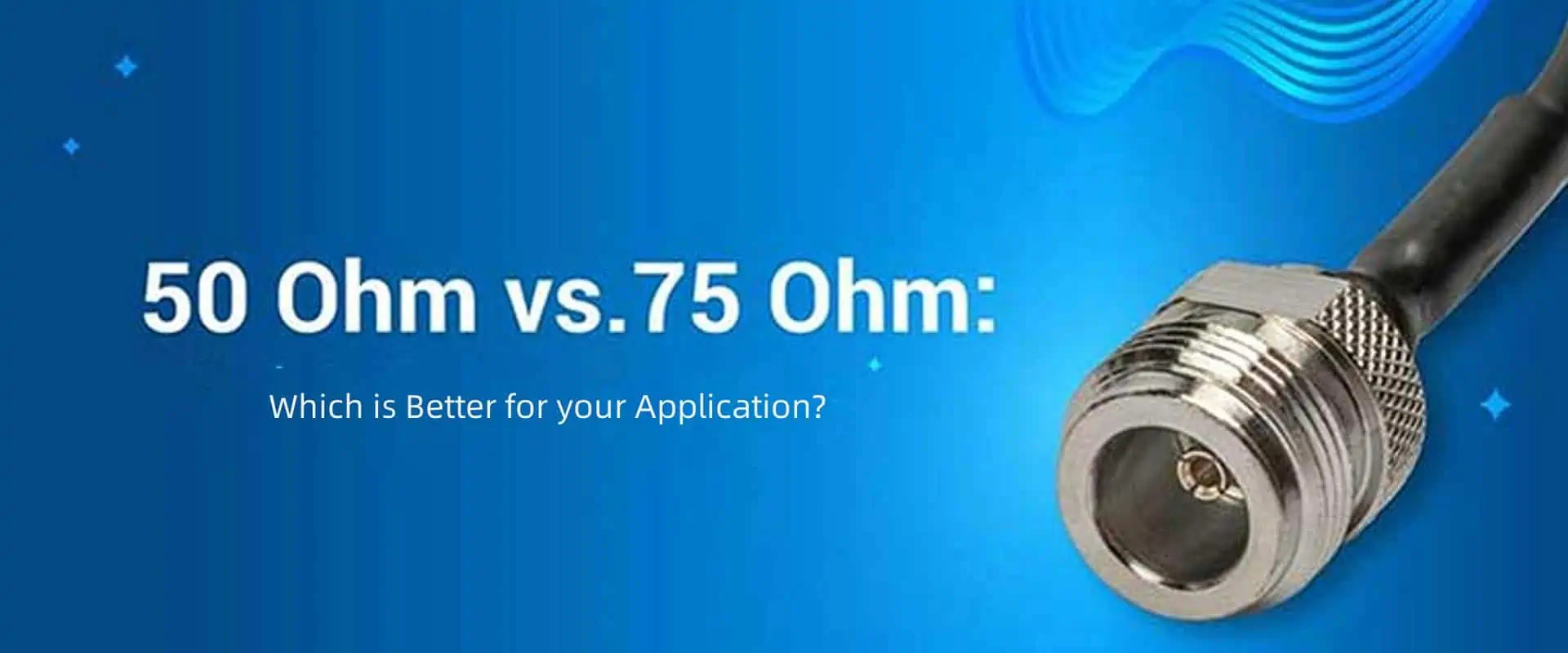
Introduction
The electromagnetic properties of soil are associated with chemical and physical variables. Magnetic susceptibility, dielectric permittivity, and electrical conductivity are the common EM properties. The chemical and physical variables include density, moisture content, and soil salinity. They are measured noninvasively by electromagnetic induction sensing. Transmission and receiving coils get separated by an intercoil distance.
And they are proportional to the soil investigation depth. Also, they are the main components of most EMI-based soil sensing devices. They have a frequency band below three hundred kHz. And are receptive to changes in magnetic susceptibility and electrical conduction. HFEMI sensors work between three hundred kHz and thirty MHz. Because of their increased sensitivity to changes in dielectric properties and electrical conductivity. They provide more detailed insights into soil parameters.
What is High-Frequency Shielding or RF Shielding?
- High-frequency fields are defined as magnetic and electric fields. They have a frequency greater than 100 kHz and less than 300 GHz.
- An antenna often emits electromagnetic fields of high frequency. They travel at light speed in free space. It allows them to deliver information and energy over vast distances.
- Field strengths decrease exponentially with distance from the transmitter. When you double the separation in free space, the power flux density will drop to a quarter of what it was.
High-frequency magnetic and electric fields have a frequency between hundred kHz and three hundred Gigahertz. Electromagnetic fields are also known as magnetic and electric fields. This is because of the strong coupling between them at high frequencies.
The electromagnetic fields’ wave nature is describable by the relationship between wavelength and frequency. This, in turn, is relatable by the speed of travel (that is, the light speed in free space). In general, wavelengths are smaller for higher frequencies and larger for lower ones. When sending signals over empty space. The wavelengths can be anything from 3 kilometers to 1 millimeter.
In today’s communications, high-frequency fields are used.
An antenna often emits EM fields of high frequency. They travel at light speed in free space. It allows them to transfer information and energy over great distances. The most common application of this quality is in contemporary methods of communication. They include:
- Broadcasting, Video, and Wireless Technologies
- The development of wireless communication technologies. For example, wireless phones and WLAN have made this possible.
The Bluetooth radio modules are an example of a short-range gadget. They employ high-frequency EM fields.
Because of the wide range of uses for HF electromagnetic fields. Modern humans are constantly bombarded by a vast range of transmitters. The field strength or intensity is either specified as follows:
- Measured in volts per meter (V/m) or amperes per meter (A/m) for electric fields or amperes per meter (A/m) for magnetic fields.
- In terms of power flux density (measured in watts per square meter, W/m2).
The strength of a magnetic and electric field is multiplied to determine the power flux density.
Propagation of High-Frequency or Electromagnetic Shielding
Field strengths decrease rapidly with separation from a transmitter. Power flux density in open space drops quadratically with distance. And halving the distance results in a one-fourth reduction. The intensity close to the transmitter might vary greatly. Even at constant distances from the source. Because several antennas, by virtue of their design, emit in different favored directions. Thus, it is impossible to determine the field strengths at a specific site from a distance only.
When high-frequency EM fields encounter obstacles in their direction of propagation, they might get absorbed or reflected. The material characteristics of the object have a specific role. They are important in determining which mechanism is dominant. As a result, the transmission of HF fields in natural settings is very different. When compared with the simplified situation described above. That involved transmission in free space.
RF Shielding
HF electromagnetic fields get reflected by conductive or magnetic material, such as metals. HF electromagnetic fields can be totally or partially shielded by materials. The materials can be metal mesh or foils, as well as metal-coated glass panes (for heat retention).
Significance of Electromagnetic Interference Shielding
Every designer and engineer working with electronic circuitry must consider electronic shielding once its nature as electromagnetic interference gets understood. Its potential consequences on its immediate environment become readily apparent. Touch or conductive EMI. Close or without interacting (capacitive and magnetic EMI) and radiating EMI (which travels further) can all have an effect on electronic devices.
Due to technological progress and the widespread use of electronics in today’s digital age. The EM wave spectrum has become severely oversaturated. This includes electric transmission and distribution system-related disturbances. As well as those caused by external factors like lightning and solar flares.
High-Frequency Electromagnetic Shielding Effectiveness
- signals received by communication equipment get distorted or jammed
- Total destruction or breakdown of the electronic system
- Power surges, spikes, and surges, as well as EFT or quick electrical changes
- Shocks and burns from electricity
- electrical systems have decreased efficiency and shelf life
- Probably Ignition Source
To solve these issues, international groups have stepped in to create EMC, or electromagnetic interference, standards.
EMC refers to the ability of some devices to perform normally in an electromagnetic environment. There shouldn’t be any electromagnetic energy production or transmission to other devices, either.
The CISPR, which is a member of the IEC, and the ISO establishes global EMC regulations.
EMI Shielding Mechanism
EMI shielding is the other practical method of implementing EMC. Alongside filtration, grounding, and bonding. This process involves building enclosures with the proper EMI-shielded material thickness, shape, and structure to redirect EM waves (either into or out of the equipment). When electromagnetic waves pass through conductive or ferromagnetic materials, their path gets modified by reflection or absorption.
Magnetic and electric fields are the two main components of electromagnetic waves. The two components are in phase with one another and move at the same speed. The electric parts of a printed circuit board (PCB) or electronic circuit device get shielded by the conductive substance. At the same time, the magnetic components get shielded by the strong magnetic permeability feature, however, because electromagnetic waves have a complement. Shielding one component safeguards the other.
Multiple reflections, absorption, and reflection are the three methods that can be used for EMI shielding.
Reflection
The EMI shielding system is the primary defense against electromagnetic interference. The electric component of electromagnetic interference gets dampened via reflection. However, mobile charge carriers in the material become important to achieve EMI reflection. This necessitates a conductive quality in the RF radiation shielding used for protection. Within the conducting shield, EM waves interact with mobile charge carriers. It causes the carriers to redistribute their charges. And generate an opposing EM field.
Due to the redistribution of charges, an electromagnetic field gets produced. It cancels out the external magnetic field. This method works. Because the properties of a shield improve with the conductivity of the material. Discontinuity is an important part of the mechanism’s design flaws. The shielding qualities of an enclosure get nullified. If the size of any hole or other discontinuity in the structure is greater than the wavelengths of the external EM field. Hence, it’s important to keep these dimensions as small as possible. While designing the enclosure. To combat stronger EM waves. Where shrinking the hole size would be futile, filtering tools can get used.
Another difficulty is the skin effect, which is more noticeable in AC circuits. It involves the buildup of charges on the surface of a conductor. The charges build up due to the passage of alternating current. As a result, there is now a higher concentration of electrical current in this region. The shielding effect and conductivity are both reduced. Since the inner segment of the conductor gets used less. Higher-frequency electromagnetic waves are more prone to this impact. Consequently, the solution is to expand the surface area of the conductor. It, in effect, expands the region’s usable cross-section. Electroplating the surfaces with conducting materials is another option. Silver or Copper can be the possible options.
Absorption
It is a method for blocking electromagnetic interference (EMI), particularly its magnetic component. The presence of electric and magnetic dipoles is necessary for EMI absorption to be achievable. These materials are notable for their high dielectric constants and magnetic permeabilities. When an external magnetic field is present. The magnetic field lines cutting through the material get disrupted. A magnetic field line can get absorbed by a container with this property. It is possible by following a path within the structure that maintains itself. However, low conductivity is a frequent issue that arises from their use. As a result, their ability to shield or safeguard electrical components degrades.
The attenuation of the incoming EM waves by the phenomenon of eddy currents is a crucial part of the absorption process. It reveals itself anytime there is a high-frequency oscillation in the electromagnetic wave. As a result, it causes the conductor’s internal currents to get induced. Their magnetic field’s eddy currents act to counteract the external field’s strength. It’s also true that eddy currents in materials with electric conductivity tend to be more robust.
Multiple Reflections
It is another mechanism discovered to predominate in compounds with large absorbent features on their surfaces or interfacial areas. Multiple reflecting barriers that reflect the EM waves serve to block out the RF radiation. As a result, the EM waves get dispersed.
Materials Used in High-Frequency Shielding
Understanding the two basic EMI shielding qualities, electrical conductivity and magnetic permeability, is essential. It is important for thorough consideration of EMI shielding materials. It’s a relief to be rid of them, given their existence was established and discussed in the prior section. However, submitting a query to RayMing PCBs and Assembly can also be useful for such components. If you’re looking for ways to protect your electronics from EMI, this company has you covered.
The question then becomes, what materials can be used for EMI shielding?
· Metals
As a simple and inexpensive EMI shielding option, it is a no-brainer. Metal is an excellent EMI-protecting material because of its nature and qualities. For example, strength, ductility, electrical conductivity, and magnetic permeability. For attenuating electric fields, silver is the most effective substance. Because of its high electrical conductivity and resistance to corrosion. Silver has a high value, but it is also very expensive in comparison to other EMI shielding materials. Therefore, silver is generally used as an electroplating coating or alloy component.
Therefore, silver is generally used as an electroplating coating or alloy component.
Copper and aluminum are the industry standards. Because they provide adequate shielding at a reasonable cost. The electrical conductivity of Copper is identical to silvers. But aluminum’s is 40% lower. Electromagnetic radiation can be effectively blocked by carbon steel. It may include carbon steel or ferritic stainless. Also useful as magnetic shielding materials are the alloys of iron-nickel, such as Permalloy, Superalloy, and Mu-metal. Mu-metal is the most popular, and it is also the most permeable, making it the most abundant.
· Carbon Allotropes
It stands for the class of carbon structures. It includes carbon fibers, carbon nanotubes, graphite, and exfoliated Graphene. Composites containing such allotropes are usable as EMI shielding agents. Its inherent strength and conductivity make it a useful material. Furthermore, they rely heavily on a shielding technique involving multiple reflections.
Because of its adaptability and its ability to flow over the surface of the sealing areas, exfoliated graphite is widely used as an EMI-protecting gasket. All the allotropes are porous structures, which aid in the reception of EM noise. The extremely high aspect ratio of Graphene, carbon nanotubes and carbon fibers makes them useful as fillers. Cement, metals, polymers, and ceramics get strengthened by embedding the fillers into their structures. But due to its smaller aspect ratio and skin depth. Graphene and carbon nanotubes are primarily useful for HF shield applications. Therefore, at gigahertz frequencies, these materials are superior conductors to metals.
· ICPs
It stands for a family of unusual polymers that may conduct electricity without any conducting components included. The popularity of ICPs rises due to their low weight and ease of processing. Because of their atomic structure, which includes conjugate bonds. Polymers that are intrinsically conductive can transmit electricity. Because of this, the free electrons can get used to charging devices. Changes are also possible to how well ICPs conduct electricity or carry a current. This sort of change is achievable through undoing or doping.
Although ICPs have been in use, the concept is continually developing. Challenges in mechanical and chemical stability exist. Despite this, they continue to be favorable as primary constituents, notably in carbon nanoparticle and filament-based composites.
What are High-Frequency Shielding Materials?
Different EMI-protecting materials are typically made from one of three different metals. When searching for the optimal EMI shielding option, engineers may often combine materials.
· Pre-Tin Plated Steel
Some metals used for EMI shielding can block frequencies up to several Gigahertz. But, pre-tin coated steel is very inexpensive. Besides this, it is very effective at blocking frequencies. The frequencies range from kilohertz to low Gigahertz. When compared to the other metals, carbon steel’s low-frequency protection properties stand out. Furthermore, it prevents the steel from rusting and corrosion.
· Copper Alloy 770 / Nickel Silver
Alloy 770, a copper alloy, goes by a few other names as well. Zinc, nickel, and Copper are their constituent elements. The best reason for its widespread use is its resistance to corrosion.
As an EMI shield, copper alloy 770 excels from the mid-kilohertz to the gigahertz band. Its permeability is one, making it perfect for use in MRI machines without the use of magnets.
· Copper
There is a distinction between Copper and copper alloys 770. Copper is the greatest EMI-protecting metal. Because it effectively dampens both electrical and magnetic waves. Copper is present in anything from complex medical devices to inexpensive personal computers because of its ability to block electromagnetic interference.
Copper is more expensive than most other alloys, including unplated steel. However, it has a greater conductivity rate, which is what makes it so useful as an EMI shielding.
· Aluminum
Aluminum is a good EMI shielding material. This is due to its higher conductivity and lightweight. Aluminum’s conductivity is about 60% lower than that of Copper.
But there is a drawback to using aluminum. It has higher oxidation characteristics than other metallic materials. Also, it erodes more quickly. When metal gets oxidized, its strength and durability get compromised.
· EMI Shielding Gaskets
Sealing the gap between 2 flat surfaces is what gaskets are for. Similarly, EMI-protecting gaskets prevent electronic components from getting damaged by electromagnetic interference.
In the past, EMI shielding was achievable by having metal sheets custom-cut. The custom cut was possible by fabricators to fit into cases. Steel, Copper, and Aluminum sheets of suitable thickness get processed in this manner. The circuits they have intended to shield will leak if the sheets get deformed by time or weather and remain in that shape.
The EMI gaskets are composed of particle-filled silicones. And resemble a ruggedized or sieve touchscreen. These gaskets can withstand both hot and cold temperatures. This makes them a great option for dealing with EMI issues.
On top of that, they are simple to make and do not require expensive components.
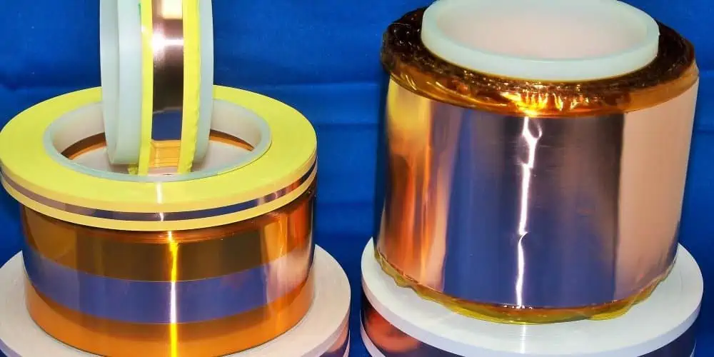
· EMI Shielding Film And Foil
There is a market for a variety of EMI shielding materials, including foil, film, and tape.
Different forms of EMI materials exist. Conducting silicones, for instance, can get installed as window films. The installation helps to protect electronics from harmful electromagnetic radiation.
The frequency range and electronics getting shielded are the two factors to consider. They determine the EMI protection’s material and shape.
To prevent electromagnetic interference, technicians wrap equipment wires in metallic foil or braid. Coaxial cables are another option. Because they incorporate EMI shielding into the actual wire design, wire bundles can get encased in foil. And cable braids can cover an entire building. Both of these are common practices for technicians.
Connectors are also shielded from electromagnetic interference (EMI) by foil or braiding connected to metal coverings.
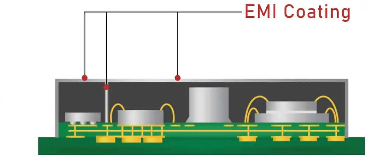
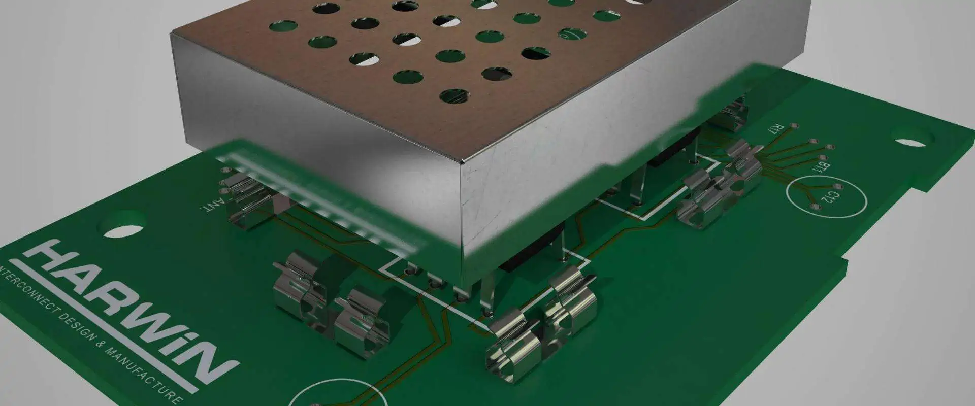
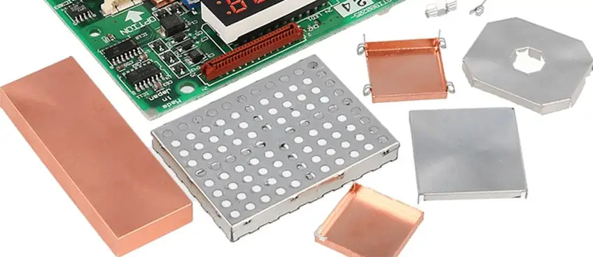
The shielding for a PCB consists of a metal enclosure. It is placed over the sensitive components and a ground plane. The technicians then set up a Faraday cage around the sensitive components.
The electromagnetic interference (EMI) from popular household appliances like televisions and microwaves get blocked by the inside steel casing of audio speakers.
Use magnetic materials and conducting points when the frequency of the magnetic field is less than a hundred kHz. Metal foam, metal sheet, conducting polymers, and metal mesh screening. These are some of the other tools used by technicians.
Foil tapes designed specifically for EMI protection have a number of desirable properties. They are both flame and corrosion-resistant. They are flat and engraved, making them easy to mold into unusual configurations.
Shielding tapes can be found from a variety of sources:
- Connector and cable grounding plates
- Computer keyboards
- across the space occupied by separate electrical parts and connections
- Wherever there are cracks or openings in a protected chamber.
- Electro-Medical Equipment
- Electronic enclosures panels and doors
- The periphery of electrical components like relays and coils that might get attracted to wideband EMI signals
- Used to shield relays, coils, and other devices from emitting harmful levels of broadband EMI
· EMI Shielding Foam
Carbon foam is another form of EMI protection that is becoming increasingly popular. Even though it contains no metal. The EMI-protecting foam is effective from a hundred MHz all the way up to twenty GHz. Because of its adaptability, foam excels as an EMI shield medium. It’s not just one of those useless things.
Some types of foam, for instance, are used to prevent fires. It is resistant to corrosion. Also, it is lighter in weight than metal and has a longer service life in extreme conditions. In addition, it has a low impact on the natural world.
· EMI Shielding Silicone
Silicone is non-conductive to electricity. In contrast, metal embedded in silicone produces a conductive substance. It is useful as an EMI shielding.
Silicone has additional benefits, like its malleability. Die cutting allows manufacturers to make a custom EMI shielding solution. They can make customized solutions for every application. EMI-protecting silicone has found applications in different departments. These include satellite communication, aerospace, automotive, and electronic device manufacturing sectors.
Silicone is well-liked by many because of its resistance to moisture and light. It is also temperature resistant. Therefore, silicone is used in fields like aeronautical engineering, where temperatures can fluctuate.
Present-day EMI shielding silicone contains nickel graphite. It efficiently blocks RF between twenty and ten thousand Hz.