how to improve fm signal on radio with a single wire antenna

NFC Antenna

Radios can be found in various locations, including shops, homes, cars, and public spaces. Their user-friendly design and cost-effectiveness have made them a popular choice among many individuals. Nevertheless, there are a few issues that one might encounter while utilizing them.

A common problem while using a radio outside the home or in an area surrounded by tall buildings is poor signal quality. This is due to the limited range of radio frequencies, typically between 400 to 470 MHz, divided into various sub-bands to meet the user’s requirements.

If you are experiencing weak FM signal reception, check out this video to learn how to enhance the signal using a simple single-element antenna:

These frequencies fall under the UHF spectrum, allowing for up to twenty various radio frequencies to coexist in a similar location. As buildings are generally not too tall, they don’t significantly obstruct the signal.

The change in signal strength may not be noticeable when you are outside. However, when you enter areas surrounded by tall buildings, you may experience a decrease in signal quality as these buildings act as a barrier to the signal.

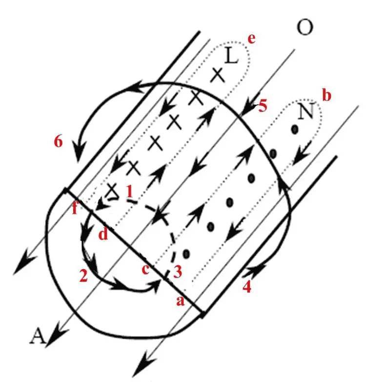
UHF (Ultra High Frequency)frequencies are commonly utilized for handheld radios due to their wider bandwidth compared to the frequencies utilized for television or radio broadcasting. However, the major drawback of using UHF is known as LOS propagation.

The signal takes a direct route instead of bouncing off objects, which is desirable for clear handheld reception. However, this can pose an issue when using the device in outdoor settings or locations surrounded by tall structures.

UHF frequencies cannot readily penetrate objects, but they can induce objects to redirect their signals. As a result, instead of following a direct route from one radio wave to another, signals are redirected by objects, leading to a distorted signal waveform.

Radio reception becomes more challenging when using the device outdoors or inside a vehicle. The signal stability is impacted due to difficulties in maintaining a constant signal.

Steps to Improve FM Signal with Only Single Wire Antenna

L Band Patch Antenna

To enhance the signal of an FM radio with a single-wire antenna, specific measures must be taken. These steps are standard, as with specific type of antenna tend to exhibit similar behavior. 

Here are the steps:

1st Step

To begin, you need to detach the Broadcasting antenna. Detaching the aerial from the means of communication will enable us to identify the arrangement of the antenna and cables so that we can assess if any modifications or adjustments are required for the system. Alternatively, it can help us determine if there’s any physical damage-related issue. Ensure to carefully remove the aerial by loosening all the screws that secure it and unplugging the antenna connector. Also, extend the antenna to its full-length capacity.

2nd Step

In the 2nd step, after removing the antenna, reattach it to the radio and turn it on. Tune in to the desired channel. Next, lift the antenna upward until it extends to its maximum height. Adjust the antenna sideways or at different angles to improve sound quality. Repeat this process until no interference is heard, which signifies excellent radio reception.

3rd Step

To ensure the radio connection stays strong, you can secure the end of the antenna with tape. Initially, you might experience a reduction in signal strength when the antenna is not being held. To combat this, keep moving the antenna until the sound is clear and the signal quality is good. Another method of testing the quality of the signal is to move around the radio and look for any signal interference. If you detect any interference while walking close to the radio, you may want to consider making modifications/ adjustments to the systems. If the radio signals are not disturbed, then the settings of the current are good to go

Improve Signals with Obstruction

FULL PCB MANUFACTURING Quote

The fluency of the radio signal can be impacted by many obstacles & materials in different locations. To enhance FM radio signals, it’s essential to follow specific recommendations. One of the critical factors that significantly impact the radio signal in buildings is the materials used in walls/ceilings, such as steel.

Recommendations:

  1. The radio should be relocated to a location with fewer obstacles impeding signal reception. In various buildings, certain materials used in walls, such as steel and iron, can hinder the flow of the radio signal. Besides the materials, other physical characteristics of the building, like the height of the building, and the thickness of the walls, also affect radio signal receptivity. The best places to locate the FM radio within a building are windows.
  2. To find out which way the antenna should face, you can try listening to a channel and see how clear the sound is. Some radios at home don’t have a big antenna and use a skinny wire instead. The power cord can also work as an antenna in some situations.
  3. If your current antenna isn’t giving you a good signal, you can add a new one to the radio system. You can use dipole antennas or the old-fashioned “rabbit ear” antennas on TV sets. Connecting a new antenna to the radio will make the FM signal stronger. You can attach the U-hooks to the screw terminals on the radio antenna. Finally, find a spot for the new antenna to get the FM signals.
  4. To improve the sound of the FM radio, switch it from “stereo” to “mono.” FM radio stations usually broadcast in stereo mode, but it can be challenging for the radio to receive a clear signal. When you use mono mode, it gets rid of the two channels, but it also makes the signal less fuzzy and with less static, which leads to a more robust sound.
  5. If the above steps don’t make your FM radio signal more precise, you may consider installing an outdoor antenna. This kind of antenna can help the signal flow without being blocked by buildings. You can buy outdoor antennas from electronics stores, just like the ones people used to have on their roofs for their TV. These antennas can significantly improve FM radio signal reception. If you get an outdoor antenna, it’s best to put it as high up as possible and connect it to the radio using a coaxial cable.

Boosting the Signals

After you adjust the antenna, you can make the signals stronger. This is what you do:

  • To get better radio signals, try to make the power cord for the radio as straight as you can. This usually helps make the signals stronger.
  • Change the audio from stereo to single sound (Mono).
  • Slowly extend the antenna and move it around to different positions. This will help you get the best signal and improve reception.
  • To make the radio work better, place it near a window. This will help it receive signals better and reduce obstacles that block the signal. Remember that the signals come from outside where the tower.
  • If you want even better reception, you can get a special dipole antenna. You can find these at an electronics store or hardware store. Please attach it to the FM input on your radio, which will help improve the radio signal.
  • To use a dipole antenna with your radio, connect it to the FM input and adjust the wire to find different stations.
  • If you live far from a transmitting tower and want better reception, consider installing an outdoor antenna outside your house.
  • Once the outdoor antenna is set up, connect the wire to the input jack on your radio. Make sure the antenna is securely attached to the roof and positioned level, not tilted.

Advantages

FM amplifiers can help make your car radio sound better. They’re quick and easy to install and only need a simple antenna. You’ll see an improvement in sound right away, and since they do not take up much room, they’re a great solution.

Conclusion

By following these tips, we can make our radio equipment work better. This way, we can always listen to our favorite stations and stay updated on important news & information, especially in an emergency.

But by using the easy tips in this blog, you can make your radio’s FM signal better with just a simple antenna. Do you’ve any problems or need help? Ask a professional for advice.

SolidWorks PCB Services, what is it all about?

SolidWorks PCB Services

Printed Circuit boards have become the main components of the electrical gadget we utilize to undertake our day-to-day activities. Therefore, if you have used an electrical device, for example, a phone, a watch, or even a laptop, you have utilized a PCB. However, most of the time, we only experience the efficiency and the optimized performance that comes with PCBs, not the struggle that goes into manufacturing these components.

Producing a Printed circuit board requires technicians to utilize complex processes that use a lot of resources and energy. However, out of the many processes that lead to the manufacturing of a PCB, the stage tends to be more crucial than the restโ€”the Designing stage. However, due to its complexity, manufacturers have developed impeccable software programs to help PCB designers. One of these incredible software programs is SolidWorks PCB. SolidWorks was initially created as a modern-era, revolutionary tech for printed circuit board design integration with three-dimensional mechanical design ENV. However, after creation, this software program offers more than just this single feature. So what exactly does the SolidWorks Printed Circuit Board Software have to offer? And why should you consider using it over other competitive software programs?

Printed Circuit Boards in a Nutshell

layout
layout

Printed circuit boards, or simply PCBs, are electronic circuits we use in electronic devices to offer electrical connectivity and mechanical support to electrical components, for example, ICs. We produce PCBs by combining various sheets of components that are non-conductive, for example, plastic or fiberglass, that can easily hold the copper circuitry.

We also refer to PCBs as Etched Wiring Boards (EWB) or Printed Wiring Boards (PWB).

A printed circuit board functions on the CU or copper circuit/assembly/films that are carefully embedded inside the non-conducive materials to offer a pathway that effectively transmits electrical current. Printed Circuit Boards can hold multiple electrical components soldered onto them without using cables. The elimination of cabling makes electrical devices that run on PCBs lighter. Moreover, it eliminates the issues that come with using cables on electrical appliances, such as higher risks of short circuits.

Printed circuit boards are present in almost every computing device and electronic gadget out there, including:

  • Graphics cards
  • Network cards
  • Motherboards
  • The internal circuitry of CD-ROM/Hard Drives

Due to their application areas, you must carefully manufacture printed circuit boards. That is because messing up might make the circuit board fail, ultimately leading to the gadget failing. And considering that circuit boards operate in critical machines such as life support machines in the medical industry, this is not something that you would want to happen.

SolidWorks Printed Circuit Board Services

FULL PCB MANUFACTURING Quote

SolidWorks printed circuit board, formerly PCBWorks, is a printed circuit board (PCB) designing tool that PCB designers integrate into the popular SolidWorks three-dimensional design software. To install this program, utilize the SolidWorks Installation manager, which installs this program as an individual installation.

Electrical engineers utilizing SolidWorks PCB can easily alter the design of a PCB and then push the alterations to a repository. Moreover, mechanical engineers using this software can also easily access the altered PCB design from the prior saved repository. After accessing this design, they can analyze any modifications made, make additional alterations, and then push the new design back to its repository, where electrical engineers can access it to make more changes.

Through this collaboration, technicians can generate high-quality and optimized PCBs. Moreover, this collaboration ensures that designers catch errors in the early stages before they move the design to production.

However, to make this collaboration possible, you must install SolidWorks Printed Circuit Board Services, which effectively manages various repositories on shared servers. The SolidWorks PCB services program installs via the SolidWorks Installation manager. Hence, it doesn’t require you to purchase a new license to use this program. Moreover, this program includes databases for storing data and sync the alterations made by various mechanical and electrical engineers. It also includes MIIS or Microsoft Internet Info Services.

In various network ENVs, you install SolidWorks printed circuit board services on a shared server that doesn’t have the SolidWorks Programs installed. Moreover, you can also install this software with various SolidWorks Printed Circuit Board components on one machine.

To ensure its efficiency and effectiveness, you must have this software running 24/7. Moreover, you must ensure it has bidirectional, uninterrupted communication through virus scanners and firewalls with users running the SolidWorks program and the SolidWorks printed circuit board software.

Key Features of SolidWorks PCB

Altium Designer 20

MCAD/ECAD Project Collaboration Server

MCAD/ECAD collaboration servers help you facilitate the collaboration between the mechanical and electrical sides of the PCB designing project.

Moreover, these servers also help you link electrical data to the mechanical models of SolidWorks CAD. Combining this information in one place enables you to manage your project better. Moreover, it also ensures seamless synchronization of information, which is crucial when working with a team.

Parasolid Support

The SolidWorks PCB services program supports the native Parasolid SolidWorks file format, which ultimately widens the scope of this software application-wise. Moreover, using this software, you can easily link parasolid models for component bodies and enclosures and then view them in three dimensions to ensure the board you are designing fits mechanical enclosures perfectly.

Copper Analysis

You can quickly improve your design’s accuracy using SolidWorks CAD and SolidWorks PCB. Moreover, this software lets you send your PCB design to the SolidWorks CAD bearing Copper information. After processing, you get back a detailed mechanical, vibration, and thermal simulation, which helps you view your design from a new angle or perspective. Moreover, this simulation can help you identify and fix errors before you move your design to production. Doing so will make your design less prone to errors after production.

Conclusion

Printed Circuit boards are a crucial aspect of the electrical industry. They help manufacturers produce compact electrical gadgets that are powerful and efficient. However, to use these circuit boards, they have to manufacture them first. During the manufacturing process of PCBs, technicians have to start from the designing phase, which is crucial. That’s because any mess made during this stage is carried forward to the production stage. However, to avoid this, you should utilize the SolidWorks PCB services program. It lets you collaborate with mechanical and electrical engineers to help you generate an efficient and flawless PCB design.

Why the Voltage Divider Formula is Important

Voltage Divider Formula

Voltage divider formula is a complete yet user-friendly tool that enables you to assess the output signals (i.e. voltage) which is produced by one voltage divider, which is frequently used for voltage regulators.

Continue reading to find out what the voltage divider formula is, its basic calculator, and the way it applies to different equations for various types of voltage divider. Learn how this voltage divider formula and rule can be used to obtain a portion of the input voltage.

Consider the myriad ways the voltage divider is used in both simple and extremely complicated systems to further persuade yourself that the electronic circuits shouldn’t be anything to get concerned about.

What Does a Voltage Divider Mean?

The voltage divider can be described as a straightforward circuit that lowers voltage. It equally distributes its input voltage amongst some of the circuit’s components. Two resistors linked in series, and with input voltages applied across its resistor pair as well as the output voltages drawn from the point in between, are the best representation of the voltage divider.

It’s employed to generate various levels of voltage from a single source of voltage while maintaining a constant current for each component in series circuits.

Voltage Divider Formula and Calculator

Inductor voltage and current waveforms

The output voltages of the voltage divider always reduce its input voltage as well as the current that flows through a series network, which is determined by Ohm’s Law, (V=IR). The current between them is equal since this current is shared by both resistors. We can figure out the voltage that was lowered across the second resistor, with the help of this formula.

The voltage passing across many resistors connected in series having a DC source of voltage can be calculated using the voltage divider formula and calculator (can handle about 10 resistors).

Calculating the entire resistance of the whole circuit in series is how the voltage divider operates. Voltage divider formula is then applied, with Resistor 1 serving as the particular resistor which we are attempting to calculate the drop in voltage across is. For each resistor in voltage divider circuits, this calculation is repeated.

The higher the resistance values of the elements, the more voltage would be lost across them, according to Ohm’s law. Likewise, less voltage passes through resistors having lower values for resistance.

The VIN, input voltage, as well as resistor values, ranging between 1 and 10, must both be entered in order to utilize the voltage divider formula and calculator (to serve multiple resistors connected in series). Then, the user must click on “Calculate” button. Each resistor entered will have its voltage drop calculated and then automatically displayed. This voltage’s outcome is calculated in volts.

The voltage divider formula for a voltage divider circuit of two resistors is Vout=Vin(R2R1+R2), while for two resistors, it is VRx=Vin(Rx/RT).

What is the Rule for the Voltage Divider?

FULL PCB MANUFACTURING Quote

The idea behind the voltage dividers indicates that though this voltage is divided in some way across the series-connected parts, the current flowing through them remains constant. To determine the precise numbers for our circuit, you must use Ohm’s law. To start, we must make the following very important information:

The only composition that applies to DC circuits is RR composition. In these circumstances, any impedance can be regarded as wires having zero resistance, and capacitances function as a circuit’s gap, where they have an infinite resistance. The rule for voltage divider is valid for the highest value of potential difference for the remaining ones, which are all employed with AC circuits. Finding a phase shift to suit these voltages might be just as useful.

Voltage Ladder

The circuit known as the voltage ladder consists of many resistors connected in series having a voltage applied across the whole network of resistors. The voltage drop of every resistor in these networks is greater than that of the one preceding it.

The current remains constant across the entire ladder because the resistors are connected in series. Divide the entire voltage by total resistance to obtain its value. By multiplying the entire current by each resistor’s value, one may determine each resistor’s voltage drop. The total of voltages lost by every resistor between a node as well as ground can be used to define the voltage referred to ground at every given node.

Input Voltage and Voltage Drop

The output voltages and divided voltage throughout the circuit are both determined by the drop in voltage across R2. Two resistors are connected in series to provide a voltage divider that is referenced to the ground.

R1 as well as R2 are connected in series to form an input voltage, while R2 receives its output voltage. There is therefore nowhere else for the same amount of current which passes through every resistive component of circuits. Therefore, this delivers a voltage drop of IxR across every resistive element as a result.

We can use the voltage law of Kirchoff and Ohm’s Law in determining the drop in voltage across every resistor based on the current flowing across them after knowing the supply voltage.

What are the Applications of the Voltage Dividers?

Below are some of the uses for voltage dividers:

A potentiometer is a well-known device that utilizes the concept of the voltage divider. This component is also known as a rheostat.

Typically, they are made entirely of resistive parts. We can differentiate between digital as well as analog ones, but we can tune the resistance using extreme precision in either case. Slide pots, trim pots, and thumb pots are some most well-liked varieties of potentiometers, and they differ in size and construction. The sliding contact, which makes it possible to alter the resistance of the output, is the key component.

Equipment for measuring high voltage – This comes out that high voltages can be measured, despite the fact that direct measurements may be harmful to the instrument. In that situation, it is practical to drop the voltage onto a secure area using a voltage divider. It is preferable to utilize capacitive devices rather than resistive ones at really high voltages.

Locating an unidentified resistance:  If you just have the voltage source as well as another resistor having a known resistance, is it still possible to detect any unknown resistance? If you’re able to understand the color code, you’re lucky, yet what happens when there isn’t?

You can, however, just build a straightforward circuit with two resistors connected in series, choose input voltage, but then gauge the voltage across the required resistance. The enigma is then solved by simply entering all of these values in to voltage divider formula and calculator. The general equation for voltage divider can always be transformed to determine.

What are the Benefits and Drawbacks of the Voltage Dividers?

Several of you might be questioning why someone would use a voltage divider for measuring an unknown resistance whenever they could merely read the amount of amperage which passes via the resistor whenever any external voltage has been appliedโ€”a straightforward application of Ohm’s law. So, generally speaking, there shouldn’t be much of a difference between both approaches, but we have to be conscious that most materials’ resistance is dependent on temperature. Even worse, the dependencies for insulators, semiconductors, and metals are different.

As metals’ resistance rises as the temperature does, we must determine the thermal coefficient of the material in order to quantify the resistance at a standard temperature. This calls for carefully measuring the surrounding temperature, performing some calculations, and hope that there were no mistakes during the meantime.

But we can make it much easier than that! You might employ a straightforward voltage divider, as you would have thought!

More Benefits and Drawbacks

Two resistors are present in the basic form, and as they are constructed out of a single material, the temperature dependence on resistance are essentially the same. These resistances vary at roughly the same rate, regardless of the size of the temperature differential. Although any change will balance out because this voltage divider formula often has the ratio of different impedances, the voltage of the output should be independent of temperature. Also, if we examine the formula from the preceding section, we’ll get a resistance value that is just like the initial one at any specific temperature.

Second, while designing some intricate electrical circuits, it’s indeed practical to utilize voltage dividers. We may employ one source as well as voltage dividers needed, as opposed to employing several independent voltage sources that each produce a unique potential inside the system.

On the contrary, we must be mindful that the drop in voltage is more likely the longer its circuit’s wires are. Although the likelihood is far lower than it would be for the long industrial cable, the issue should still be considered and ideally avoided wherever possible if we have to perform some precise measurements.

Conclusion

What we’ve previously accomplished demonstrates how the voltage dividers function for the most basic systems. Second, it’s practical to utilize voltage dividers while creating some.  One can probably guess they are utilized nowhere in reality and that more advanced circuits are typically employed.

Yet, all of the aforementioned findings may be useful in order to simplify more complicated ones. For example, you may treat a group of resistors as one single resistance if you are able to see them arranged in a series or parallel.

The design process and working principle of a water alarm sensor

water alarm sensor

What is a water alarm sensor?

A water alarm sensor is a tool used to detect the presence of water in a specific location. It notifies the user of a possible flood or leak. We can install water alarm sensors in various places, including basements, bathrooms, kitchens, and laundry rooms. They usually are battery-powered.

In regions vulnerable to flooding or water leaks, water alarm sensors can be especially helpful in averting water damage. They may give homes and businesses an extra layer of security, are reasonably priced, and are simple to install. In addition, water alarm sensors can assist in reducing damage by rapidly spotting potential water leaks or floods, ultimately saving time and money.

Design Process

Water presence sensors should notify the user of a potential water leak or flood by detecting the presence of water in a specific region. The following steps are part of the design process for water alarm sensors:

Requirements gathering:

We first gather the specifications for the water alarm sensor as the first phase in the design process. This entails figuring out the sensor’s level of sensitivity requirements, the environment it will work in, and its intended use case.

Component selection:

water alarm

After establishing the specifications, we must choose the components utilized in the water alarm sensor. This involves picking the power source, microcontroller, wireless connectivity, and sensing component.

Schematic design:

The water alarm sensor’s electrical connections between its many parts appear in depth in the schematic design. The sensors, microprocessor, wireless module, and power source are all part of this.

PCB layout design:

The physical design of the circuit board used in the water alarm sensor is called the PCB layout design. The components’ locations, routing of the traces, and the enclosure’s size and shape are all crucial in the layout design.

Prototype development:

After completing the schematic and PCB layout designs, we create a water alarm sensor prototype. This entails putting the Board together and testing the sensor in real-time.

Testing and validation:

We test and validate the water alarm sensor to ensure it satisfies the requirements acquired in the first step of the design process. Testing the sensor’s sensitivity, accuracy, and response time is part of this process.

Enclosure design:

Designing the enclosure for the water alarm sensor is the last phase in the design process. The enclosure must be lightweight, water-resistant, and simple to install in its intended location.

Final testing and validation:

The last stage is to test and validate the sensor. This ensures it complies with the necessary standards. Finally, it should be ready for usage after creating and properly assembling the enclosure and the water alarm sensor, respectively.

It is crucial to remember the intended use case for the water alarm sensor throughout the design process and to ensure that the finished product satisfies the user’s needs. This entails considering elements like the required sensitivity, the sensor’s environment, and the degree of wireless connectivity needed for the sensor to communicate with other systems or devices.

How does a water sensor alarm work?

FULL PCB MANUFACTURING Quote

In the event of a probable water leak or flood, a water sensor alarm should detect the presence of water in a specific area and notify the user. A water sensor alarm’s essential operation entails employing a sensing element to detect the presence of water, processing the signal using a microcontroller, and setting off an alert or notification using wireless connectivity.

A water sensor alarm’s detecting component may depend on several technologies, including optical detection, electrical conductivity, and capacitance. The most widely used sensors are those based on electrical conductivity since they are inexpensive and simple. These sensors measure the electrical conductivity of the water, which varies with the water’s concentration of dissolved ions.

A microcontroller processes the sensing element’s output, processing the data to determine whether water is present and setting off an alarm or notice. The microcontroller can perform several functions, including adjusting the sensor’s sensitivity, checking the battery level, and establishing communication with other systems or devices.

The microcontroller can start an alarm or notification when the sensor detects water using Wi-Fi, Bluetooth, or cellular communication. As a result, even if they are not physically present in the area where the sensor is, the user can receive a real-time notice about a water leak or flood.

Specific water sensor alarms can do additional actions, such as shutting off water valves or turning on pumps to stop more water damage, in addition to setting off an alarm or warning.

Where should water sensors be placed?

water leak alarm

We can install water sensors in locations where water leaks or floods are most likely to happen. However, it’s crucial to remember to install water sensors in various locations around a facility for maximum security. Also, it is essential to routinely check the sensors to ensure the batteries are charged and operating properly. Water sensors can assist in preventing water damage by following these instructions, ultimately saving time and money. Water sensors are frequently in the following locations:

Basements: Because they are at the lowest point of a structure and frequently run the risk of water seeping in from the surrounding soil, basements are particularly vulnerable to floods.

Bathrooms: Water leaks frequently happen in bathrooms, especially near sinks, toilets, and showers.

Kitchens: Water leaks are also possible in kitchens, especially around sinks and dishwashers.

Laundry rooms: We can install water sensors close to washers or dryers, which, if not maintained properly, can leak or overflow.

Appliances that leak or overflow if not properly maintained include refrigerators, air conditioners, and water heaters. We can install water sensors close to these appliances.

Crawl spaces: Although frequently disregarded, they may become a source of water leaks if pipes or other components break.

We can install water sensors near sump pumps, which drain excess water from a basement or elsewhere.

Summary

A water alarm sensor helps to detect the presence of water in a specific location and notify the user of a possible flood or leak. We can install battery-operated water alarm sensors in various spaces, including laundry rooms, basements, bathrooms, and kitchens.

Using a detecting component, the sensor locates the presence of water and wireless connectivityโ€”such as Wi-Fi, Bluetooth, or cellular communicationโ€”then initiates an alarm or notice. As a result, even if they are not physically present in the area where the sensor is, the user can receive a real-time notice about a water leak or flood.

In regions vulnerable to flooding or water leaks, water alarm sensors can be especially helpful in averting water damage. They may give homes and businesses an extra layer of security. Water alarm sensors are affordable and are simple to install. In addition, water alarm sensors can assist in reducing damage by rapidly spotting potential water leaks or floods, ultimately saving time and money.

The Essential Factors to Take into Account While Building Ultra-Thin PCB

0.2mm thin pcb board

An ultra-thin PCB is a form of printed circuit board that is thinner than conventional PCBs. They are perfect for situations where space is premium or weight reduction is essential because they are generally less than 0.8mm thick.

Smartphones, laptops, tablets, and other portable electronic gadgets frequently employ ultra-thin PCBs. These PCBs’ thinness makes it possible to create electrical devices that are lighter and smaller, which is crucial in today’s mobile environment.

Specialized techniques and materials, such as thinner copper foil, thinner substrate material, and smaller vias, are needed to manufacture an ultra-thin PCB. Therefore, producing ultra-thin PCBs may be more difficult and costly than conventional PCBs due to these procedures and materials.

Smaller, lighter, and more portable electronic gadgets rely heavily on ultra-thin PCBs.

Ultra-thin PCB manufacturing calls for particular thought and attention to detail. The following are some crucial factors that must be taken into mind while creating ultra-thin PCBs:

Substrate Material:

flex pcb capability

The PCB’s foundation layer, the substrate material, supports the copper foil and the electronic parts. The substrate material for ultra-thin PCBs must be as thin as is practical while offering sufficient stiffness to avoid bending or flexing. For ultra-thin PCBs, common substrate materials include polyimide, PET (polyethylene terephthalate), and FR-4.

Copper Foil:

Copper foil for ultra-thin PCBs must be thinner than a copper foil for conventional PCBs. Depending on the demands of the particular application, the copper foil’s thickness is generally between 9 and 18 m. The lighter and thinner copper foil contributes to a reduction in the PCB’s overall thickness and weight.

Vias:

Vias are tiny holes punched into the PCB to facilitate power transfer and communications across its various layers. To prevent weakening the substrate or copper foil on ultra-thin PCBs, we must consider the size and positioning of the vias. The through’s diameter should be as small as feasible to reduce the distance the signal must travel. Additionally, the via should be as close to the component as possible.

Component Placement:

We must carefully consider component placement on the board to keep the ultra-thin PCB as small as feasible. Therefore, the components should be positioned near the PCB surface to reduce the overall thickness. Also, if possible, we should use surface-mount components or components with a low profile.

Solder Mask:

To prevent solder bridges from developing between neighboring pads and to shield copper traces and pads from oxidation, we apply a layer of material known as a solder mask on the PCB. To lower the overall thickness of ultra-thin Boards, the solder mask must be as thin as feasible.

Trace Width and Spacing:

We must carefully evaluate its width to ensure the PCB’s traces can transport the necessary current without overheating. Furthermore, the distance between the traces is essential to prevent cross-talk and signal interference.

Thermal Management:

All PCBs should consider heat dissipation, but ultra-thin PCBs require extra care. It is more difficult to disperse heat due to the thin substrate and copper foil. Therefore thermal management must be given additional consideration. This can involve the application of thermal vias, heat sinks, and other cooling strategies.

Flexibility:

Ultra-thin PCBs are frequently essential in applications where flexibility is necessary, such as wearable technology or flexible displays. As a result, the PCB needs to be flexible without sacrificing its structural integrity. We may accomplish this through flex-rigid PCB design, flexible substrate materials, and careful component arrangement.

Testing:

Because of their fragility and thinness, evaluating ultra-thin PCBs might be more difficult than testing regular ones. Therefore, we must prevent PCB damage during testing to guarantee reliable testing findings. Specialized testing equipment could also be necessary.

Manufacturing Processes:

Ultra-thin PCB fabrication procedures might be more complex and call for specialized tools. For instance, during manufacturing, the thin substrate and copper foil would need to be handled with more care, and the tiny vias could need more accurate drilling tools.

Which are the Quality Standards for Ultra-Thin PCB?

FULL PCB MANUFACTURING Quote

Ultra-thin PCBs must adhere to several quality requirements, and doing so will help guarantee that the boards are reliable and of the necessary quality. The following list of ultra-thin PCB quality requirements includes some of the most popular ones:

IPC-6013:

This is the requirement for Flexible Printed Board Qualification and Performance Specification. It includes the specifications for flexible printed circuit boards, including ultra-thin PCBs, in terms of design, components, manufacturing, testing, and performance.

IPC-6012:

The Qualification and Performance Standards for Rigid Printed Boards are available in this standard. It includes the specifications for rigid printed boards, including ultra-thin PCBs, in terms of design, components, manufacture, testing, and performance.

IPC-A-600:

The Acceptability of Printed Circuit Boards standard is here. It gives visual criteria for examining and assessing the quality of the printed circuit boards and includes the standards for the craftsmanship of printed circuit boards, including ultra-thin PCBs.

ISO 9001:

The requirements for a quality management system are available in this quality management standard (QMS). This standard’s adherence aids in ensuring that ultra-thin PCBs come with a constant degree of quality.

UL Guidelines:

The independent safety science firm UL (Underwriters Laboratories) creates safety standards for various items, including PCBs. The ultra-thin PCBs assist in guaranteeing that performance and safety criteria are met by adhering to UL standards.

RoHS:

A directive from the European Union called “RoHS” forbids using several hazardous substances, including PCBs, in electrical and electronic equipment. The ultra-thin PCBs are devoid of dangerous substances like lead, mercury, and cadmium, thanks to compliance with RoHS.

REACH:

The European Union’s REACH legislation, which stands for Registration, Evaluation, Authorization, and Restriction of Chemicals, strives to guarantee the safe incorporation of chemicals into goods. REACH compliance guarantees that ultra-thin PCBs are free of dangerous substances that might endanger human health or the environment.

What is the Purpose of Shielding in Ultra-Thin PCB?

Ultra Wide Band (UWB) Antenna PCB

Shielding is helpful in ultra-thin Boards (EMI) to prevent electromagnetic interference from damaging electronic circuitry. However, when electromagnetic radiation from one source obstructs the operation of another electronic equipment, this unwelcome phenomenon known as EMI occurs. This interference in ultra-thin PCBs may originate from adjacent equipment, power supplies, or other electromagnetic sources.

Electronic circuits can experience various issues due to EMI, including noise, distortion, signal loss, and poor overall performance. By building a wall between the EMI source and the electrical circuit, shielding helps to stop this interference.

Shielding on ultra-thin PCBs often entails the placement of a conductive layer between the electronic circuit and the EMI source. This layer helps to reflect or absorb the electromagnetic radiation generating the interference.

Shielding in ultra-thin PCBs might include other elements besides the conductive layer, such as ground planes or vias, which create a low-impedance path for the EMI to dissipate. These parts direct EMI away from the electrical circuit, lowering the possibility of interference.

Shielding in ultra-thin PCBs serves the general aim of insulating electronic circuits from the detrimental effects of EMI, assuring their dependability and interference-free operation. Furthermore, ultra-thin PCBs are an excellent option for various industries and applications because they operate well in high-frequency or high-speed applications through shielding.

The Advantages of Ultra-Thin PCB

The Advantages of Flexible Printed Circuit Board

Compared to conventional PCBs, ultra-thin PCBs provide several benefits, including decreased size and weight, enhanced signal and thermal performance, superior reliability, cost-effectiveness, more design freedom, and a smaller environmental footprint. They are a popular option for many applications because of these benefits.

Disadvantages of Ultra-Thin PCB

While choosing a PCB technology for a specific application, it is essential to consider both the benefits and drawbacks of ultra-thin PCBs. They include issues with temperature control, signal loss, manufacturing complexity, design limitations, and fragility. These drawbacks may restrict the PCB’s performance and dependability in high-temperature applications.

Applications of Ultra-Thin PCB

Due to its many advantages over conventional PCBs, ultra-thin PCBs are essential in various applications. Among these are smartphones, wearable technology, consumer electronics, consumer goods, automobiles, the Internet of Things (IoT), sensors, and smart cities. They are perfect for wearable devices worn on the body since they may be flexible, stretchy, and conformable. They can also tolerate high vibrations and temperatures.

The Digital circuit design Process and its advantages

BGA Layout Tutorial

The process of developing digital circuits that can carry out a range of activities, from straightforward logical processes to intricate computational functions, is known as digital circuit design. From determining the circuit’s needs to testing and confirming the design, there are various processes involved in the design process. In this post, we’ll go over the fundamentals of designing digital circuits and give a general overview of the procedure.

Overview of Digital Circuits

Digital circuits are electronic circuits that express information using digital signals. Because digital signals are binary, they can only have two possible values: 0 and 1. Voltage levels help express these values, with 0 normally represented by a low voltage level (for example, 0 volts) and one typically represented by a high voltage level (e.g., 5 volts). Simple logic operations like AND and OR, as well as more advanced computing tasks like arithmetic and logic operations, can be carried out by digital circuits.

Combinational circuits and sequential circuits are the two broad types into which digital circuits fall. Combinational circuits are those that generate an output solely based on the values of the current inputs. While their output solely depends on the most recent input data, they lack memory components. On the other hand, sequential circuits have memory components and generate outputs that depend on the current and past input values.

The Design Process

bare PCB layout design to cut cost

The digital circuit design process encompasses multiple steps, from determining the circuit’s needs to testing and confirming the design. However, the fundamental steps in the design process are as follows:

Requirement Analysis:

Identifying the needs of the circuit is the first stage in the design process of a digital circuit. This entails determining the purpose of the circuit and any design limitations, including a budget, power consumption, and performance standards.

Design Specification:

The next stage is to draft a design specification outlining the circuit’s specifications in great detail. The circuit’s inputs, outputs, and behavior for any possible combination of input values must all be specified.

High-Level Design:

Making a high-level circuit design comes once the design requirements are complete. This entails determining the components that will help to construct the circuit and the connections between these components to form the entire circuit. Along with the high-level design, a circuit block diagram should illustrate how the various components are connected.

Detailed Design:

The real circuit schematic, a precise circuit diagram that displays the individual components and their connections, is created during the detailed design phase. Also, choosing the individual transistors, capacitors, and resistors that will help to construct the circuit is a part of this process.

Simulation and Testing:

It is crucial to simulate and test the circuit design when the circuit schematic is complete to ensure it functions as intended. This entails testing the circuit under many settings, such as various input values and various ambient variables, by simulating its behavior using software tools.

Fabrication and Testing:

When the simulation and testing process is complete, one must build and test the actual circuit to ensure it functions as predicted. Building the circuit with the chosen components and testing it in various scenarios to ensure it complies with the design specification requires doing this.

What are the main five components of a digital system?

FULL PCB MANUFACTURING Quote

These five elements combine to build a digital system capable of carrying out various tasks. The processor unit can carry out operations on the data stored in memory and carry out instructions by receiving input from input devices. The system can then communicate with other devices and systems via communication interfaces and display the results of these computations on output devices. A digital system’s primary elements consist of the following:

Communication Interfaces:

The digital system connects to other components or systems using communication interfaces. Ethernet connections, USB ports, and wireless communication technologies like Bluetooth and Wi-Fi are a few examples of communication interfaces. The digital system can communicate with other systems and devices via these interfaces to exchange information and commands.

Output Devices:

The outcomes of the computations performed by the digital system display on the output devices. The output devices might be speakers, printers, or monitors. These gadgets transform the digital signals the digital system generates into a human-friendly format.

Memory:

Data and instructions are kept in memory for the processing unit to access. In a digital system, primary and secondary memory are the two fundamental forms. As the processing unit works on them, data and instructions are temporarily stored in primary memory, commonly known as random-access memory (RAM).

Processing Units:

The component of the digital system that handles computing is the processing unit. It typically consists of a microprocessor or central processing unit (CPU), which is in charge of carrying out operations on digital data and carrying out instructions.

Input Devices:

The digital system receives input from input devices. Mice, touch screens, keyboards, and mice are a few examples of input devices. These tools let people communicate with the digital system and input data as digital signals.

Advantages of digital circuit

PCB layoutย lineย design
PCB layout line design

Digital circuits are electronic circuits that run on binary digital signals that indicate whether an electrical voltage or current is present or absent. Due to their various benefits, these circuits are essential in various electronic devices, including computers, smartphones, and televisions. Seven benefits of digital circuits are as follows:

Reduced Signal Degradation:

Signals can be transmitted over long distances by digital circuits with little signal deterioration. This is so that we can preserve the integrity of digital signals over extended distances.

Compatibility:

Since most modern electronic gadgets use digital signals, digital circuits are compatible. This makes the integration of digital circuits with other electronic systems and devices simple.

Flexibility:

Digital circuits are very adaptable since they are simple to reprogramme and reconfigure. This is so because discrete parts like easily replaceable or modifiable logic gates make digital circuitry.

Low Power Consumption:

As binary signals only have two states, they are helpful in digital circuitry, which uses less power than analog circuits. This indicates that less power is needed to change the signal’s condition.

High Accuracy:

Since binary signals clearly distinguish between the on and off states, digital circuits function with high accuracy. This enables digital circuits to carry out accurate actions with minimal error.

Easy to Store and Transmit:

Because we can represent them using binary digits, digital signals are simple to store and send. This facilitates the storage and transport of substantial volumes of data, which is essential for applications like digital processing, data storage, and communication.

High Noise Immunity:

Binary signals, which can be either high or low voltage, are used to run digital circuitry. These signals are less vulnerable to noise and interference than analog signals. As a result, the operation of digital circuits becomes more dependable and accurate.

Disadvantages of digital circuit

pcb layout design
pcb layout design

Digital circuits have several benefits over analog circuits but also have certain drawbacks. The following list of five drawbacks of digital circuits:

Propagation Delay:

Propagation delay is the time a signal takes from one point in a digital circuit to another. In applications that need high-speed or real-time processing, this delay may introduce latency or timing mistakes into the circuit.

Limited Frequency Response:

Compared to analog circuits, digital circuits are more limited in their frequency response. This is so because discrete components used in digital circuits are tuned to function at particular frequencies. As a result, digital circuits’ poor frequency response might hinder their effectiveness in high bandwidth applications like wireless transmission or digital signal processing.

Nonlinear Behavior:

Although digital circuits can behave nonlinearly, they can work with binary signals on or off. This is so because transistors, which are switching components found in digital circuits and which, occasionally behave in a nonlinear manner. As a result, unwanted harmonics, distortion, or oscillations can result from a nonlinear activity.

Limited Resolution:

Digital circuits can function at specific voltage or current levels. However, because of its low resolution, it may be challenging to measure or regulate particular parameters precisely. This is especially a problem for high-precision applications like scientific apparatus.

Complexity:

Designing and building digital circuits might be more challenging than analog circuits. This is because digital circuits consist of discrete parts, such as logic gates, which we can combine to create circuits of greater complexity. In addition, with additional gates, digital circuits get more complex, making troubleshooting and debugging more challenging.

The future of digital circuit design

Digital circuit design is a fast-developing discipline with a lot of potential for creating new electronic systems and gadgets. The following are some of the major areas that will influence digital circuit design in the future:

More Emphasis on Energy Efficiency:

Digital circuit designers emphasize energy economy as energy consumption becomes more urgent. Digital circuits’ power consumption reduces by voltage scaling, dynamic voltage and frequency scaling (DVFS), and power gating. Additionally, innovative design strategies like approximation computing will compromise accuracy for energy efficiency.

More Focus on Security:

Designing secure digital circuits is becoming more important due to the growing threat of cyberattacks. Manufacturers protect the integrity of the digital circuit by methods like secure boot and hardware security modules (HSMs), which stop unwanted access and modification. Furthermore, new encryption and authentication approaches will also increase the security of digital circuits.

More Advanced Design Tools:

As the complexity of digital circuit designs increases, designers are using more sophisticated design tools to manage the complexity and improve the performance of their circuits. For example, high-level synthesis (HLS) and artificial intelligence (AI) will automate the design process and raise the caliber of the finished design. Also, new simulation tools will make it possible to simulate digital circuits more quickly and accurately.

Higher Levels of Integration:

To make electrical gadgets smaller, cheaper, and more energy efficient, digital circuit designers are attempting to pack more functionality onto a single chip. Adopting system-on-chip (SoC) and system-in-package (SiP) architectures, which combine numerous functionalities, including processor, memory, and communication, into a single package, is helping to achieve this.

More Advanced Process Technologies:

Digital circuit designers rely on more sophisticated process methods to address the demand for more potent and energy-efficient electronic gadgets. In addition, due to their distinct electrical characteristics, novel materials like graphene and carbon nanotubes are being investigated for application in digital circuits. 

Top Examples and Applications of IIoT Manufacturing

IIoT

Industrial IoT (IIoT) refers to integrating devices, machinery, & sensors into a network that connects to the Internet. The primary objective is to gather data and perform data analysis for ongoing process enhancement. Various IIoT applications are currently available, and this new paradigm has encouraged numerous companies to adopt it to enhance productivity, optimize expenses, and increase profits. 

The IIoT market is continuously growing, with layers already implementing it. Although studies provide varying estimates of the market value of IIoT in the upcoming years, the most significant reports indicate that investment will enhance at least threefold.

It would be prudent to gain an understanding of the primary IIOT applications and also how to apply the system to gain a competitive advantage.

Applications of IIoT Manufacturing 

According to studies released by Deloitte, the corporate world places significant importance on creating IoT environments. In their “Industry 4.0” report, 94 percent of survey participants indicated that Digitalization is a crucial strategic goal for their organization. 

Although this trend is observed worldwide, in the industrial sector, companies should recognize the significance of IIoT applications in developing sustainable processes for the future.

ยท Automated & remote equipment management

One of the principal Industrial IoT ( Internet of Things ) applications is the automation of equipment management, which enables the centralized system to manage & monitor all processes of the company.

The capacity to manage equipment remotely through digital machines & software also means that it is feasible to control multiple plants situated in several geographical locations.

This endows companies with an unparalleled capability to observe the progress of their manufacturing in real-time, as well as the ability to analyze historical information related to their processes. Collecting and utilizing this data fosters an environment where informed decisions are prioritized and support the enhancement of processes.

ยท Predictive maintenance

Predictive maintenance involves identifying the requirement for machine maintenance before a crisis occurs, which could result in an urgent halting of production. Therefore, it is one of the reasons for implementing a system for data acquisition, management, and analysis. 

Among the most compelling IoT applications is a system that works through sensors installed on machines & operating platforms. These sensors can send alerts when certain risk factors emerge. For instance, sensors that monitor machines or robots submit data to the platforms, which analyze the data received in real-time and apply advanced algorithms capable of issuing warnings when parameters such as high temperatures/vibrations exceed normal limits. 

ยท Faster implementation of improvements

Industrial IoT provides valuable information to the individuals responsible for improving processes within a business model, such as process, quality, or manufacturing engineers. They can access data & analyze it more fastly and more efficiently, allowing them to make the necessary process adjustments remotely. This also speeds up the application of changes and improvements in operational intelligence & business intelligence, which offer competitive benefits to many businesses.

ยท Pinpoint inventories

Automated inventory monitoring is another important application of Industrial IoT( Internet of Things) systems. It ensures compliance with plans and alerts the relevant personnel in case of any deviations, helping to maintain a consistent & efficient workflow.

ยท Quality control

Another critical IIoT application is the capability to check the quality of products at every stage: from the raw materials used in the process to their transportation through innovative tracking applications to the response of the end client upon receiving the product.

The data collected through the monitoring of product quality at all stages is crucial for analyzing the efficiency of a company and making necessary improvements.ย Thisย includes promptly detecting any issues in the production chain and optimizing processes. Moreover, in industries like pharmaceuticals or food, where risks must be minimized, this monitoring is particularly essential.

Industrial examples of IIoT Manufacturing 

FULL PCB MANUFACTURING Quote

Many industrial giants have already embraced the Industrial Internet of Things and reported positive results. Let’s take a closer look at their expertise.

Caterpillar

In the 1990s, Caterpillar, a United States Fortune 100 company that produces heavy machinery, incorporated IIoT into its operations. It is one of the successful instances of IoT implementation in the United States. The company now has over 500,000 assets worldwide, making it the largest connected fleet in the industry.

The company implemented IIoT for predictive maintenance of machines & fleet monitoring & management, but it did not stop there. Caterpillar now produces products with built-in Industrial Internet of Things technology capabilities for its customers. For example, their excavators are considerably easy to operate than traditional ones.

Additionally, Caterpillar’s implementation of IIoT positively impacts its clients by improving equipment & machinery utilization. For example, via predictive maintenance, the company was able to save over $600,000 for one of its mining clients, while another client reported a 20% increase in productivity through the use of Caterpillar’s autonomous vehicles.

Shell 

Shell, a major global oil & gas company based in the UK and the Netherlands, successfully implemented IoT( Internet of Things) sensors in a project in Nigeria, resulting in a cost savings of over one million US dollars through continuous monitoring of oil fields. That system was designed to track the state of some pipelines, including their temperature and pressure.

During the implementation process, Shell faced challenges related to the rugged terrain of the pipeline’s location, long-distance connectivity, and scalability. However, the final solutions successfully overcame these complications.

Komatsu

Komatsu, a mining machinery manufacturer based in Japan, has reported significant improvements in Industrial Internet of Things implementation. The company has developed its own IoT(Internet of Things) system, KOM-MICS, which collects data from sensors installed on tools & robots. Thanks to a continuous flow of information, the company was able to enhance the machine operation rate by 25%.

Subsequently, with the emergence of cloud computing, the company opted for Microsoft Azure to store the information collected from the machines. This facilitated the process of expanding and integrating more machinery from their branches worldwide into the KOM-MICS system.

First-Choice for Manufacturing and Production – Shenzhen PCB

Shengyi S1190 PCB

China is the leading manufacturing country of PCB assembly. Shenzhen is considered a leading center of PCB assembly in china. Shenzhen is currently located and based in Baoan District with a center of Shajing.

The Shenzhen Printed Circuit Board assembly sector has grown quickly for more than 40 years in part because of the comprehensive local Printed Circuit Board supply chain, technological strengths, strong capital, low labor costs, and simple transportation.

In Shenzhen, there already exist over 2,000 PCB assembly enterprises. Among the many Shenzhen Printed Circuit Board assembly enterprises, some of these are PCBA producers, and some are distributors. Everyone prefers to place orders with producers directly rather than through trading firms.

Among all the Printed Circuit Board Assembly companies, some concentrate on complex assembly for industrial, automotive, commercial uses, and defense, while others concentrate on simple PCB assembly for traditional circuits, like single, double-layered PCBs and prototypes. It’s simple to order Shenzhen PCB assembly services, but you must locate a source manufacturer whose PCBA production skills match your product specifications or positioning.

Advantages Of Shenzhen PCB Manufacturing and Assembly

shengyi pcb material

There are certain reasons why Shenzhen is considered one of the leading and most favorable places for printed circuit board assembly. Among those various reasons, some are described below.

ยท Worldโ€™s Biggest Electronic Distribution Center

Huaqiang North, the largest distribution center for electronic components in the world, is located in Shenzhen.

Enterprises from all around the world that produce electronic devices buy parts from Shenzhen and then export their goods to other countries. Finding every electronic component on BOM takes one hour in Huaqiang North, but it takes around 22 hours elsewhere.

ยท Complete Shenzhen PCB Assembly Industry Supply & Support System:

A PCB manufacturing company requires supply and collaborating partners to complete the process of PCB assembly. The partners include solder paste makers, electronic component vendors, machine distributors, shipping companies, etc. 

Entire PCB assembly manufacturers, suppliers, and services may be found in Shenzhen. Moreover, Shenzhen’s PCB assembly prices are lower than those in the United States and Europe, partly because of the city’s convenient full supply chain.

ยท Experienced Shenzhen PCB Assembly Engineers

Electronics experts and professionals from around China are drawn to Shenzhen because it is a leader in electronics manufacturing and international trade. Also, Shenzhen is home to numerous industries that manufacture electronics with foreign investment. They have been around in Shenzhen for many years and have produced a large number of skilled workers and Chinese engineers in the Assembly of the PCB sector.

Additionally, the PCB assembly sector in Shenzhen is boosted by affordable labor rates and easy access to transportation. Shenzhen PCB assembly is more competitive compared to other locations worldwide as a result of these benefits.

Shenzhen PCBAs A First-Tier Choice For Production 

FULL PCB MANUFACTURING Quote

Shenzhen is also referred to as “the silicon valley of hardware,” and there is an additional term that refers to Shenzhen, which is “Shenzhen speed.” It would be wise to look for a PCB assembly supplier in China that is located in Shenzhen since this will guarantee production speed, component availability, and the least amount of delays during the PCB fabrication process. 

Speed is undoubtedly a factor to take into account while constructing a PCB assembly prototype in China. The competent, youthful, and talented engineers located in Shenzhen will work fast and effectively to complete the assembly process within hours because prototypes are typically built by hand.

Another factor to consider is that, particularly in Shenzhen, the prototype of PCB assembly in China is frequently simpler than anywhere else in the world. Prototypes only need a few components, and those parts may be bought and acquired within one day in locations like the “HuaQiangBei” tech market and also from other suppliers and manufacturers who are located in China and have stock on hand in their warehouses.

1. Labor & Professional Hands:

When you fabricate your equipment in China, you can rest easy knowing that your hardware task is in capable hands. China, and Shenzhen in particular, draws a lot of young talented engineers who want to acknowledge their dreams. These engineers frequently work in PCBA manufacturing centers to gain experience and knowledge and build better hardware-oriented expertise. Labor costs frequently have an impact on price, and PCBasic’s PCB assembly quotation is quite alluring to many international clients. China PCB manufacturing companies always work to keep costs low without compromising manufacturing quality.

2. Machinery & Equipment:

Printed circuit board assembly (PCBA) requires a certain kind of gear and equipment, which is sometimes quite expensive. PCBA in China often has access to machinery that really isn’t common but is frequently utilized in quality assurance and testing, among other advantages. PCBasic, a Chinese provider of PCB assembly, takes particular satisfaction in extensive and cutting-edge PCB equipment, which enables it to guarantee that every product leaves the workshop in flawless functioning order. It’s only one of many reasons why PCB board assembly is made in China; certain of the equipment used in PCBasic is copyrighted and private, unavailable elsewhere.

3. Sourcing Components:

It’s time to start manufacturing once you select the best facility to make your PCBA, making sure that it is well-equipped with the newest technology and equipment. To fabricate PCB arrangements in China, you will have to source various varieties of components. The majority of the componentsโ€”or their substitutesโ€”are already widely used and available on the Chinese market, so it is simple to find stock available even during times of global shortage of components. 

4. Shipping & Logistics:

It is time to deliver the manufactured product to the client when receiving a PCB assembly estimate for constructing the product in China, acquiring all the essential components and ensuring their quality, and executing all the testing required to check performance and quality. When working with PCB components, logistics and shipping are crucial stages. Particularly when working with PCB components that have special needs, like LiPo batteries as well as other parts sourced during the process of PCB assembly in China, these devices need to be packed with additional care to ensure they are delivered to the destination state safely.

The fundamental difference between COB chip and LED

COB chip

What is a COB chip?

A COB chip is a sort of packaging where several chips are put directly onto a substrate or circuit board without requiring individual encapsulation. COB stands for “Chip on Board.” COB chips typically consist of dozens to hundreds of tiny chips connected in parallel and put on a common metal or ceramic substrate.

Because of their excellent efficiency and power density, COB chips have grown in popularity recently. They are a popular option for various lighting applications since they may offer more light output with less energy use than conventional chips. Furthermore, COB chips are frequently smaller than conventional LED chips. It makes them a viable choice for applications requiring a small form factor.

The Basics of Chip on Board (COB)

A printed circuit board (PCB) is directly mounted with an unpackaged semiconductor chip using the Chip on Board (COB) method, which also requires wire bonding the chip to the PCB. Doing away with the requirement for an external package and lowering the number of interconnects results in a more reliable and compact electronic device.

The COB procedure includes the following steps:

Die Attach: A die-attach machine mounts the semiconductor chip onto the PCB. Then, the chip adheres directly to the Board using conductive adhesive or solder.

Wire Bonding: Little copper, aluminum, or gold-plated wires link the chip to the Board after mounting it. Instead, a wire bonding machine connects the wires.

Encapsulation: We apply a protective resin or epoxy to the wire-bonded chip. It protects against environmental elements like moisture, temperature, and mechanical stress.

The following are only a few advantages of COB technology:

Size and Weight: Because COB technology does not require a separate chip container, electronic products can be made smaller and lighter.

Reliability:ย COB technology removes the danger of package failure due to temperature cycling, vibration, or mechanical stress by directly connecting the analog chip to the Board.

Cost: COB technology can lower manufacturing costs because it does not require a separate chip package or interconnects.

LED lights, automotive electronics, consumer electronics, and medical equipment frequently employ COB technology.

Differences between LED and COB

FULL PCB MANUFACTURING Quote

LEDs and COBs, two separate lighting technology kinds, are widely used in several applications. However, while they have certain things in common, they also differ significantly from one another.

Chip on Board and Light Emitting Diode both go by the acronym COB. COB is a particular application of LED technology that entails installing several LEDs on a single circuit board. LED is a solid-state lighting technology that uses a semiconductor to produce light. The following are some of the main variations between these two lighting techniques:

Design and construction

The structure of LED and COB lighting is the key distinction. LEDs are tiny semiconductor chips emitting light when exposed to an electric current. Plastic packaging that helps to both protect the semiconductor from the outside elements and offer electrical connections is typically used to house them.

Contrarily, COB lighting entails directly putting several LED chips on a printed circuit board (PCB) and fusing them together via wire bonding. A phosphor film is next applied to the LEDs to create white light.

Light output and intensity

Compared to individual LEDs, COBs often produce light with a higher intensity. This is so that they can produce a focused beam of light due to the tight mounting of the individual LEDs on a COB.

Unlike the LEDs on a COB, which are close together, LEDs typically produce light with a lower intensity. Yet, they can be employed in various applications because they may be produced in various sizes and forms.

Efficiency and energy consumption

Since COBs produce more light with less energy than individual LEDs, they are often more efficient. This is due to the close mounting of the LEDs on a COB. It then lowers the energy lost as heat.

On the other hand, LEDs are less effective than COBs because they produce light of lesser intensity and are not close to each other. Though, they are still more effective than conventional lighting methods like incandescent lights.

Color rendering

In general, COBs are more precise at reproducing colors than individual LEDs. This is so because a COB’s phosphor coating generates a wider light spectrum than a single LED. Because of this, COBs are more suitable for uses like photography and art display, where color fidelity is crucial.

On the other hand, the restricted range of light that LEDs can produce can make it challenging to reproduce colors precisely. However, improvements in LED technology have made it possible to develop LEDs. They can generate a wider spectrum of light, making them more appropriate for uses where color fidelity is crucial.

Price

In general, COBs cost more than individual LEDs. This is because they require more manufacturing processes and resources. After all, they consist of numerous LEDs on a single PCB. Since cost is less of an issue, COBs are better suited for applications where strong light output and color accuracy are crucial.

On the other hand, because they are easier to make and use fewer materials, LEDs are typically less expensive than COBs. This makes LEDs more suitable for lighting in homes or businesses where cost is the main consideration.

What voltage is COB Chip?

COB LED

A COB (Chip on Board) chip’s voltage might change based on the product’s design. For example, according to the size, power rating, and intended application of the COB, COB LEDs can run at low voltage, typically between 2V to 50V.

The manufacturer’s datasheet offers details on the chip’s electrical properties like the operating voltage, current rating, and power consumption. It contains information on the voltage needs of a COB. Therefore, it is crucial to check the datasheet thoroughly to ensure the COB is compatible with the power supply and other application parts.

A constant current driver, instead of a constant voltage supply, is frequently essential for COBs to function successfully. This is so that a constant current driver can help ensure the COB receives a stable and consistent current. However, a COB’s current draw can vary based on the temperature and other external factors. Because of this, it’s crucial to choose a constant current driver that complies with the voltage and current demands of the COB chip.

COB Chip lifespan

A COB (Chip on Board) chip’s lifespan can vary based on several variables. They include the caliber of the materials used, the environment in which it operates, and the current and voltage levels it faces while in operation.

A high-quality COB chip typically has a lifespan of 50,000 to 100,000 hours or more, substantially longer than that of incandescent or fluorescent lights. As a result, even with constant use, a COB chip can last several years.

The operating temperature can also affect how long a COB lasts because too much heat will shorten the chip’s life. As a result, it’s crucial to ensure the COB properly cools. The operating temperature should stay within the manufacturer-recommended range.

It’s important to remember that a COB chip’s lifespan depends on how long it takes for its lumen output to decline by 70%. The chip may continue to produce light after this, but it will be considerably less bright.

Summary

In conclusion, the choice between LED and COB lighting technologies depends on the application’s particular requirements. Both lighting technologies offer advantages and limitations. While LEDs are ideal for applications where cost is the main consideration, COBs are ideal for those where excellent light output and color accuracy are crucial.

The future and applications of Medical Electronics Engineering

Medical Robotics Companies

Engineering and medical science combine in the specialist field of medical electronics. It entails creating tools that can treat medical issues and enhance healthcare delivery.

The health team needs biomedical engineers because they use their understanding of biology and medicine to create novel medical gadgets. For example, they aid in creating prosthetic limbs and artificial organs.

Digitalization

Designing for the automobile or healthcare sectors, in particular, increasingly emphasizes the need for digitization. The capacity to store and access data from anywhere at any time is only one of its many benefits.

Digitalization is changing how medicine is developed and made available to patients in the medical sector. It improves productivity and lowers expenses by assisting medical professionals in reaching diagnostic and treatment decisions more quickly.

Computational simulation is a crucial aspect of digitalization to determine device performance and durability for medical devices. For instance, finite element analysis (FEA) enables designers to model potential failure scenarios for medical devices.

Medical electronics engineers must also consider legal regulations, manufacturing certifications, validation standards, and concerns associated with obsolescence for obsolete or old components. This is particularly true given the increased desire for compact, sophisticated, connected devices that can meet various regulatory requirements and hit the market fast on the part of medical OEMs.

3D Bioprinting

Medical Devices PCBA

There are several uses for 3D bioprinting, such as disease modeling and drug screening. However, the most exciting is the use of 3D-manufactured organs for transplantation.

Patients may be able to print their organs using their cells or stem cells, doing away with the necessity for organ donors. In the US, there are presently about 120,000 persons waiting for a kidney, liver, or heart.

Although printing an entire organ sounds far-fetched, developments are occurring quickly. For instance, scientists at Tel Aviv University have successfully built a 3D heart from a patient’s biological components.

Robotics

We can use robots for many jobs, from moving hazardous products to providing medical treatment. For example, hospitals and clinics employ them to assist medical professionals in completing activities without jeopardizing their safety and effectiveness.

Also, these robots are employed more frequently to reduce surgical human error. They can execute precise movements and take over low-level duties while the surgeon concentrates on high-level work.

Robotics training for surgeons is another usage for them. Doctors can rehearse treatments and enhance their skills using robotic controls on simulation platforms that combine AI and VR.

Safety, quality, and efficiency are crucial elements determining how robotics will develop in healthcare. We should consider these aspects to give patients and their healthcare practitioners the greatest results.

Artificial Intelligence

A technology called artificial intelligence enables computers to learn and analyze data. Many uses exist, such as number plate recognition systems and self-driving cars.

AI assists medical professionals in the diagnosis and better monitoring and treatment of patients’ conditions. Also, it minimizes the necessity for invasive treatments and improves specialists’ decision-making.

Before they are essential in clinics and hospitals, AI solutions must overcome numerous obstacles. They include ensuring these technologies are reliable, efficient, and morally upright.

The usage of AI technology will also require training for healthcare personnel. These professionals will require the ability to evaluate data, apply it efficiently, and comprehend human-machine interaction.

Applications of Medical Electronics Engineering

FULL PCB MANUFACTURING Quote

Engineers specializing in medical electronics use their knowledge of biology and medicine to create tools that address issues with health. These tools include stethoscopes, glucose meters, pacemakers, and defibrillators.

The performance reliability of electronic medical equipment is essential because it frequently performs life-sustaining tasks. Therefore, engineers prepare for routine maintenance using parameters like mean time to failure (MTBF) and mean time to recalibrate (MTTR).

Pacemakers

An electronic device called a pacemaker monitors your heart’s rhythm and administers electricity to maintain a regular beating. Doctors treat several disorders with pacemakers, including bradycardia (slow heartbeat) and tachycardia (rapid heartbeat).

A pacemaker can help patients live longer. A pacemaker also gives beneficial medical data that can aid your doctor in choosing the right course of treatment for you.

A lead that sends electrical impulses to your heart muscle is attached to modern pacemakers and placed in the chest and belly. These leads are attached to a tiny electrical generator and a microcontroller that tracks the electrical impulses generated naturally by your heart.

The first battery-operated pacemaker was developed in the late 1950s by a Minneapolis electrical engineer called Earl Bakken and his brother-in-law, a founder of Medtronic. Manufacturers hermetically seal the lithium iodide battery to shield it from atmospheric pollution and consist of a solid electrolyte/separator.

Patient Monitoring Systems

Systems for monitoring patients’ vital signs, such as blood pressure and blood oxygen saturation, are electronic equipment. Additionally, they spot anomalies and warn clinicians when values are too high or too low.

Patient monitors come in different varieties. While some have a few options for showing various pieces of information, others can track various factors.

Health professionals can remotely monitor their patient’s vital signs using remote patient monitoring (RPM) systems, which then electronically transmit the information to them. This enhances clinical judgments made by clinicians and leads to better results.

Implants

We can replace organs and blood arteries missing from a person with medical implants. These gadgets could be electronic devices or built of biological materials like silicone, titanium, and apatite.

Patients with physical conditions like heart disease, brain injury, and deafness use implants. They can also help to monitor and manage bodily processes.

A pacemaker, which controls heart rate using microelectronics and sensors, or a cochlear implant, which can recognize and encode sound, are two common applications of implants in medical electronics engineering.

These devices are typically implanted directly into the body and are automated so that the patient does not have to activate them for them to function actively. Doing this lowers the chance of infection and protects the implant from the body’s environment.

Artificial Limbs

Amputees who have lost their natural limbs due to sickness or injury can use prosthetic limbs created specifically for them. A prosthetist, a physician, and a physical therapist create these devices to fit the patient’s physique.

Combining several materials, including metals, plastics, and carbon fibers, produces a prosthetic limb. These materials have a variety of characteristics, including density, corrosion resistance, load-bearing capacity, Young’s modulus, and strength.

Electrodes inserted in the residual limb muscles are one way to accomplish this. This enables the patient to transmit electrical signals that cause the mechanical limb’s muscles to contract.

Another strategy entails building a sensory interface that routes nerves from the natural limb to the prosthetic limb’s surrounding skin. Using a process called sensory substitution, amputees may eventually be able to experience touch with their mechanical hands.

Top 10 medical electronics engineering companies in the world

Medical PCB Assembly

Companies that specialize in designing, developing, and producing medical devices and equipment are known as medical electronics engineering businesses. These businesses play a critical part in the healthcare sector by giving medical personnel the necessary equipment to diagnose, treat, and monitor patients. The top 10 medical electronics engineering businesses in the globe according to revenue, product line, and market share include:

Siemens Healthineers

A market leader in medical technology, Siemens Healthineers offers a wide range of point-of-care testing, laboratory diagnostics, and medical imaging products and services. Siemens Healthineers is a leader in the medical electronics engineering sector, with over 50000 people and operations in over 70 countries.

General Electric Healthcare

A branch of the General Electric Company, General Electric Healthcare offers medical technologies such as imaging, diagnostics, patient monitoring, and medical software. In addition, the company provides various products and solutions to satisfy the requirements of healthcare professionals and patients everywhere.

Philips Healthcare

A division of the Netherlands multinational technology corporation Royal Philips is Philips Healthcare. The business provides various medical products and services like patient monitoring, diagnostic imaging, and healthcare informatics. With operations in more than 100 nations, Philips Healthcare is one of the world’s top engineering firms for medical electronics.

Medtronic

Medtronic, a leading medical technology provider, creates and produces equipment for various medical disciplines, including orthopedics, neurology, and cardiology. With operations in more than 160 nations, Medtronic is one of the biggest medical device firms in the world.

Abbott Laboratories

Leading healthcare provider Abbott Laboratories focuses on discovering, producing, and marketing a broad range of nutritional, diagnostic, and medicinal products. Products are available for cardiology, diabetes, neuromodulation, and other specialties from the company’s medical device division.

BD (Becton, Dickinson, and Company)

BD is a multinational medical technology provider that focuses on designing and producing diagnostic tools, lab apparatus, and medical devices. Hospitals, research facilities, and clinics are just a few healthcare environments where the company’s goods are employed.

Stryker Corporation

The Stryker Corporation is a market-leading medical technology provider focusing on designing and producing tools and devices for various medical disciplines, including orthopedics, neurology, and surgery. The business offers a wide range of products and services to satisfy the requirements of healthcare professionals and patients everywhere.

Johnson & Johnson

The pharmaceutical, medical device, and consumer health industries are all served by the multinational firm Johnson & Johnson. For example, surgery, orthopedics, and cardiovascular disease products are available from the company’s medical device section.

Boston Scientific Corporation

The research and production of medical devices for numerous medical specialties, such as cardiology, neurology, and urology, is the focus of Boston Scientific Corporation, a top medical technology provider. The company offers a comprehensive range of products and solutions to satisfy the requirements of healthcare professionals and patients everywhere.

Thermo Fisher Scientific

Thermo Fisher Scientific is a prominent biotechnology corporation with various goods and services for the analytical, diagnostics, and life sciences markets. In addition, the company’s medical device division makes products for clinical diagnostics, drug discovery, and research.