Best Practices for Efficient Electronic Device Assembly

Electronics panel board manufacturers

Electronic Device Assembly plays a crucial role in bringing innovative products to market. This process involves the intricate task of putting together various electronic components to create functional devices, from smartphones and laptops to complex industrial equipment. As consumer demand for electronic devices continues to surge, manufacturers face increasing pressure to streamline their assembly processes, maintain high quality standards, and reduce production costs.

Efficient Electronic Device Assembly is not just about speed; it’s about precision, quality, and sustainability. In this comprehensive guide, we’ll explore the best practices that can help manufacturers optimize their assembly processes, ensuring they stay competitive in the ever-evolving electronics industry.

Understanding the Electronic Device Assembly Process

Key Stages of Assembly

To truly grasp the intricacies of Electronic Device Assembly, it’s essential to understand its key stages:

  1. Design: The foundation of any electronic device, where engineers create detailed schematics and layouts.
  2. Prototyping: Building and testing initial models to validate the design.
  3. Component Sourcing: Procuring high-quality parts from reliable suppliers.
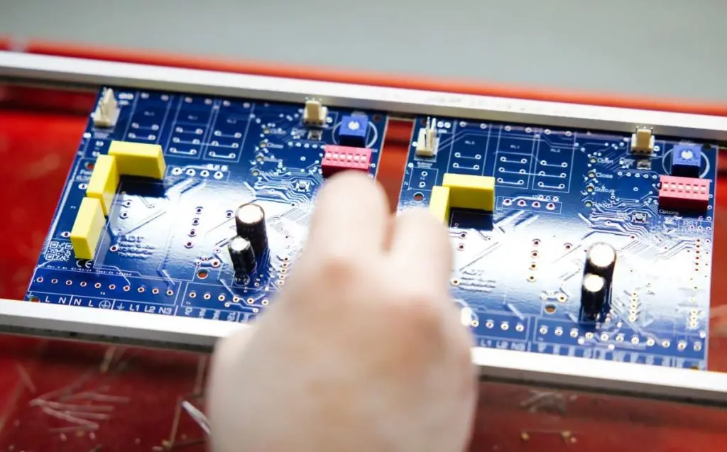
  4. Assembly: The actual process of putting components together, often involving both manual and automated steps.
  5. Testing: Rigorous quality checks to ensure the device functions as intended.

Common Challenges in Device Assembly

Despite advancements in technology, Electronic Device Assembly still faces several challenges:

  • Miniaturization: As devices become smaller, assembly becomes more complex.
  • Component Compatibility: Ensuring all parts work seamlessly together.
  • Quality Control: Maintaining consistency across large production runs.
  • Time Constraints: Meeting tight deadlines without compromising quality.

Understanding these challenges is the first step in developing strategies to overcome them and improve overall efficiency.

Preparing for Assembly: Essential Pre-Production Steps

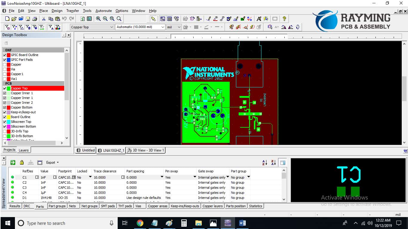
The Importance of Precise Schematics and Documentation

Before assembly begins, having detailed and accurate schematics is crucial. These documents serve as the blueprint for the entire assembly process, ensuring that:

  • Every component’s placement is clearly defined.
  • Electrical connections are accurately mapped.
  • Assembly teams have a clear reference point.

Investing time in creating comprehensive documentation can significantly reduce errors and rework during the assembly phase.

Selecting the Right Components and Suppliers

The quality of the final product is only as good as its components. When sourcing parts:

  • Prioritize Reliability: Choose suppliers with a track record of consistent quality.
  • Consider Lead Times: Ensure suppliers can meet your production schedule.
  • Evaluate Cost-Effectiveness: Balance quality with budget constraints.
  • Look for Flexibility: Suppliers who can adapt to changing needs are invaluable.

Quality Control Measures Before Production Starts

Implementing rigorous quality control measures before assembly begins can prevent costly mistakes:

  • Component Inspection: Thoroughly check all incoming parts for defects.
  • Compatibility Testing: Verify that all components work together as intended.
  • Documentation Review: Ensure all assembly instructions are clear and up-to-date.

By addressing potential issues early, manufacturers can avoid disruptions during the assembly process.

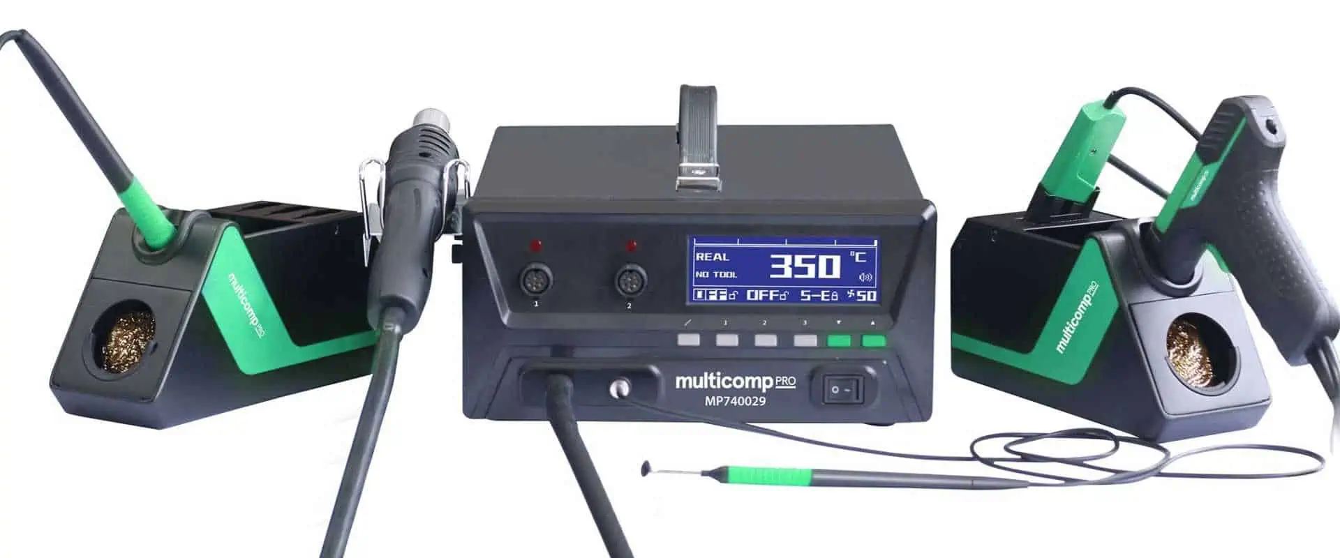
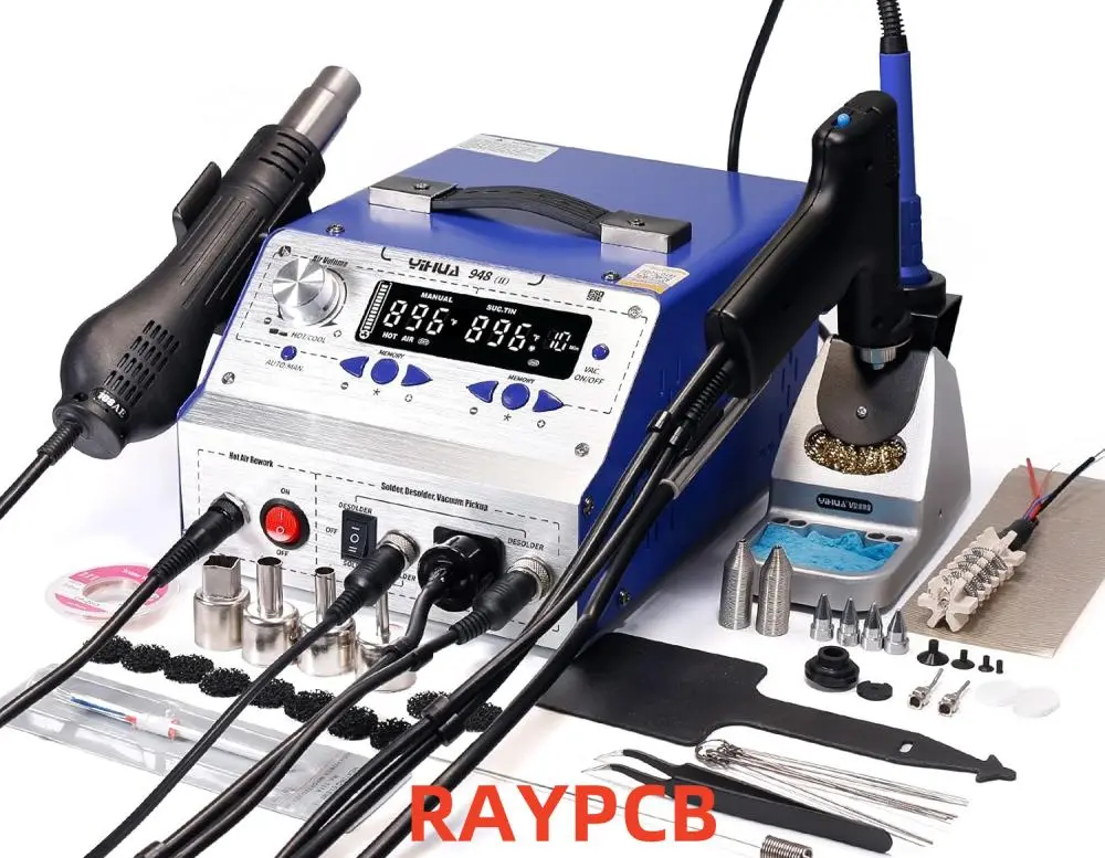
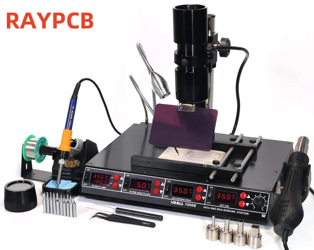
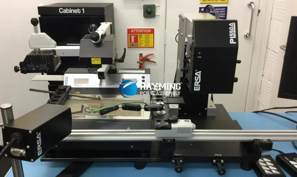
Tools and Equipment for Efficient Electronic Device Assembly

Must-Have Tools for Assembly

Equipping your assembly line with the right tools is essential for efficiency and quality:

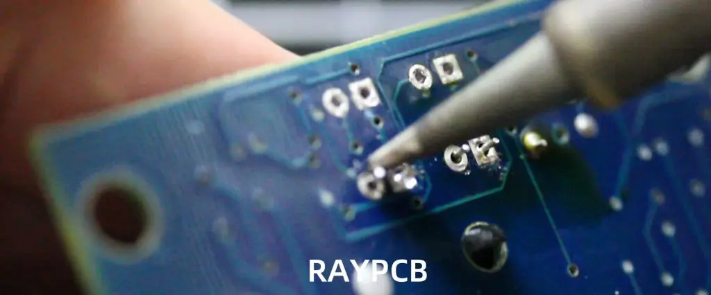
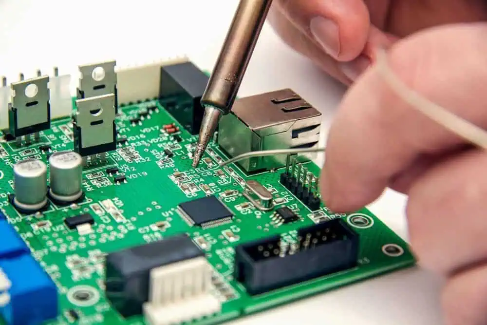
  1. Soldering Stations: High-quality soldering irons with temperature control for precise connections.
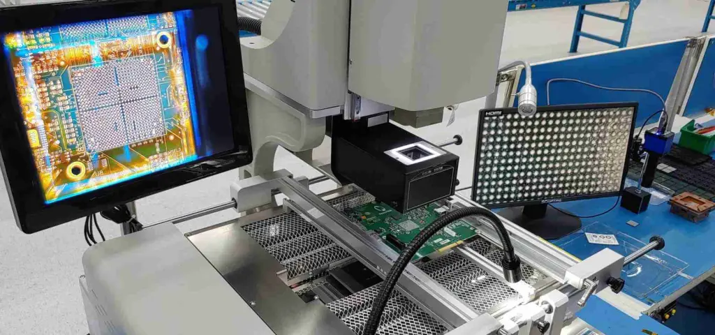
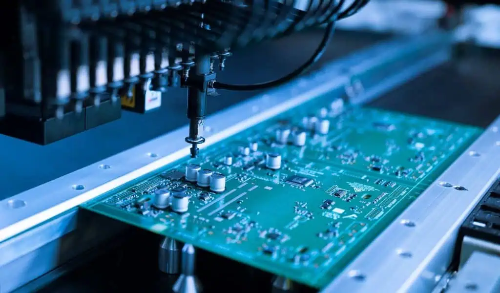
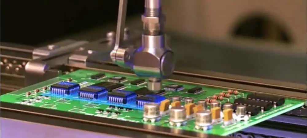
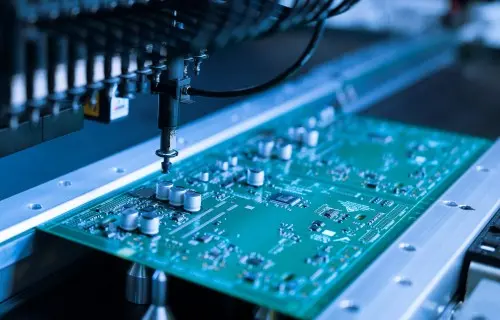
  2. Pick-and-Place Machines: Automated systems for accurately placing components on PCBs.
  3. Inspection Tools: Microscopes and magnifying glasses for detailed visual checks.
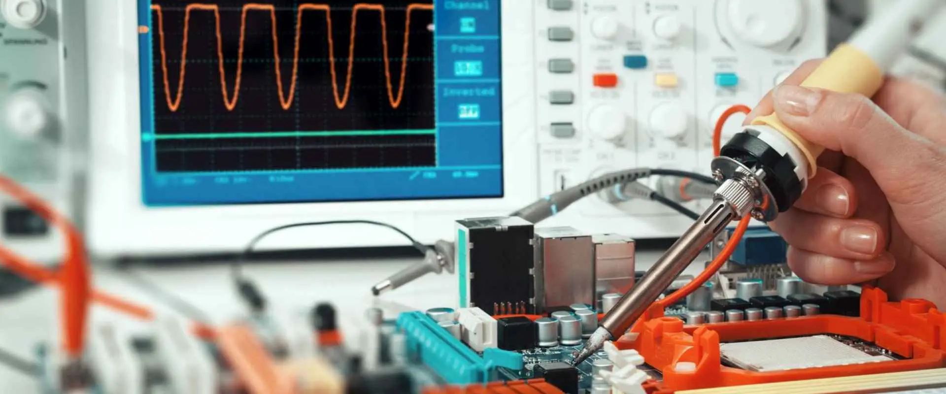
  4. Multimeters and Oscilloscopes: For testing electrical connections and signals.
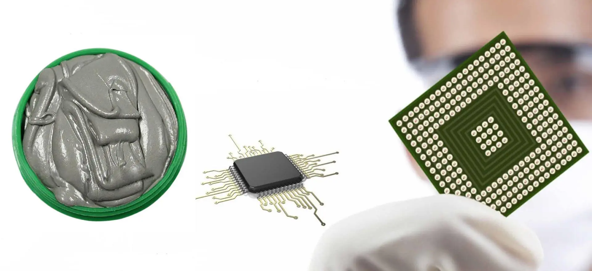
  5. ESD Protection Equipment: To prevent damage from static electricity.

How Automation Improves Speed and Accuracy

Incorporating automation into the assembly process can lead to significant improvements:

  • Increased Consistency: Automated systems perform repetitive tasks with high precision.
  • Higher Production Rates: Machines can work faster and longer than human operators.
  • Reduced Human Error: Automation minimizes mistakes caused by fatigue or distraction.
  • Real-Time Quality Control: Many automated systems include built-in inspection capabilities.

While the initial investment in automation can be substantial, the long-term benefits in terms of efficiency and quality often justify the cost.

Read more about:

Best Practices During Assembly

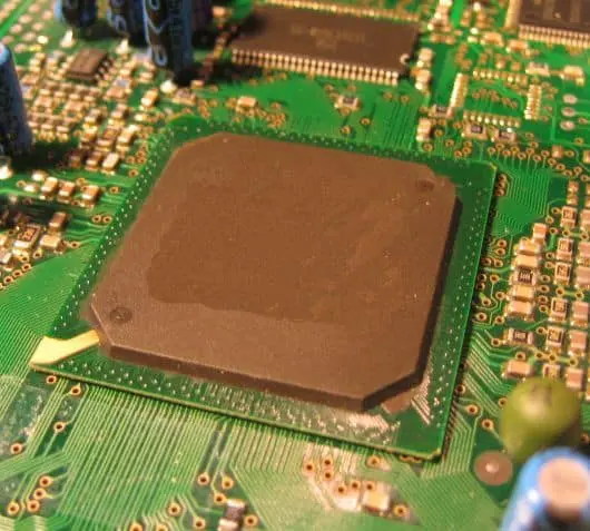
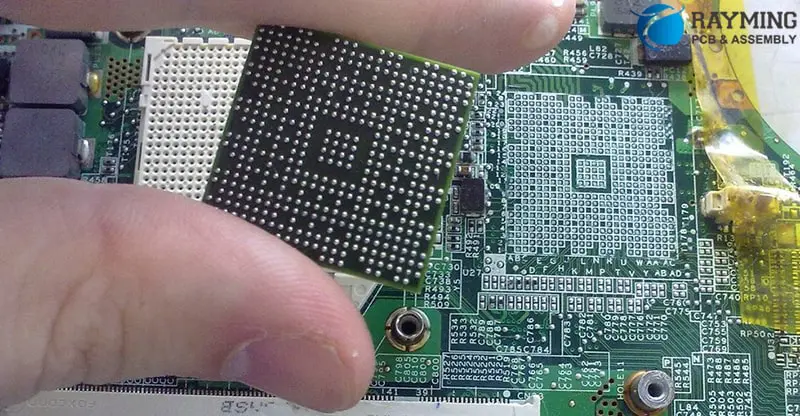
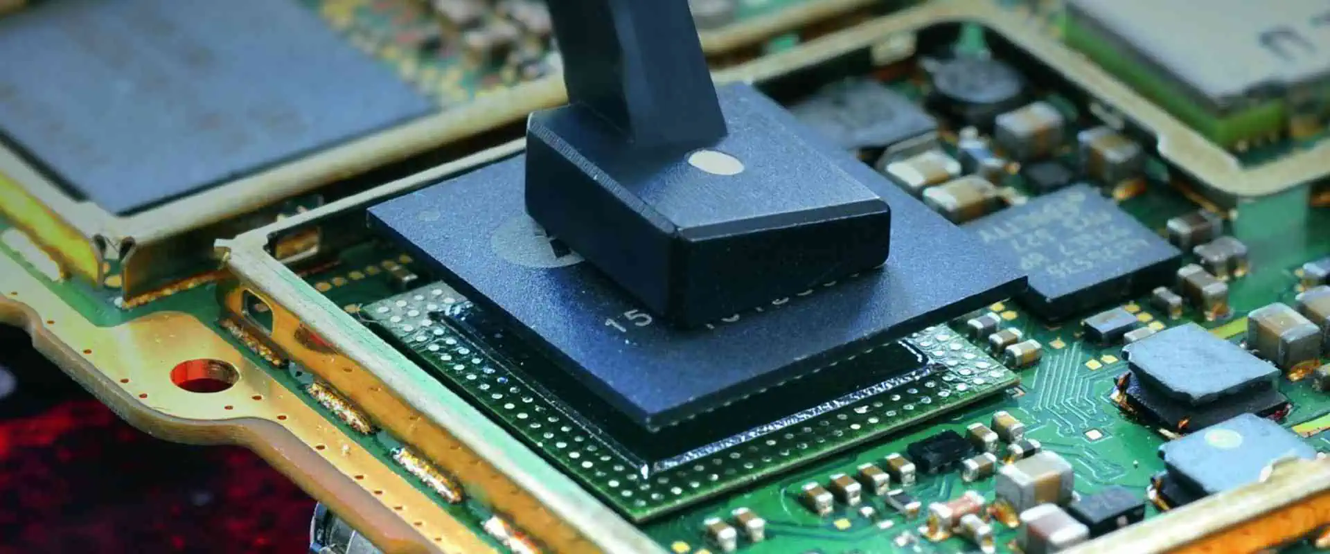
Proper Handling of Sensitive Electronic Components

Electronic components are delicate and require careful handling:

  • Use ESD-Safe Equipment: Ensure all workstations are properly grounded.
  • Train Staff: Educate assembly teams on proper handling techniques.
  • Control Environment: Maintain appropriate temperature and humidity levels.
  • Implement Clean Room Practices: Minimize dust and contaminants in the assembly area.

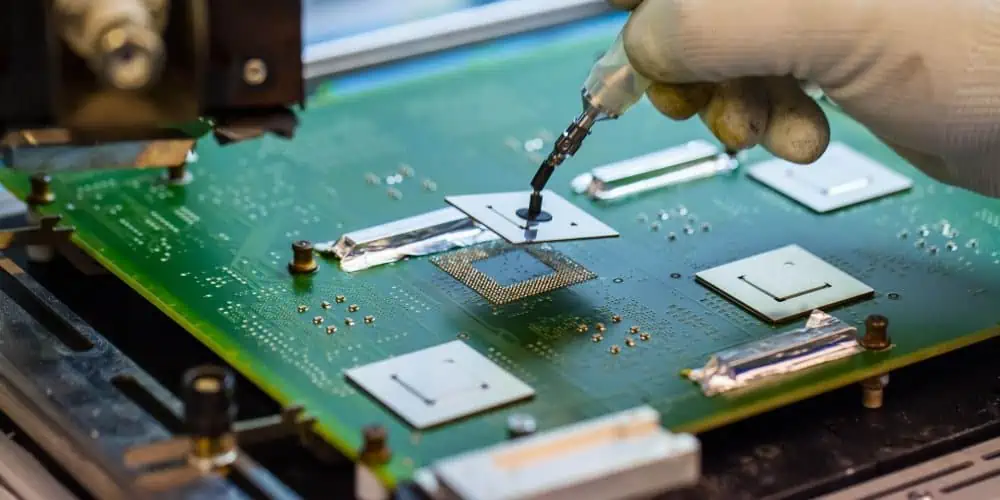
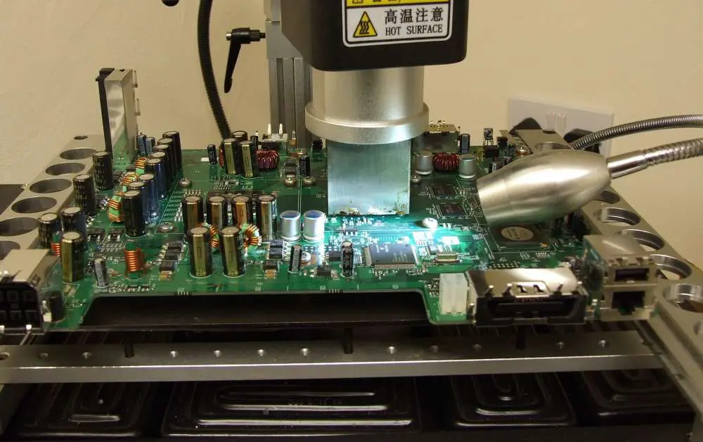
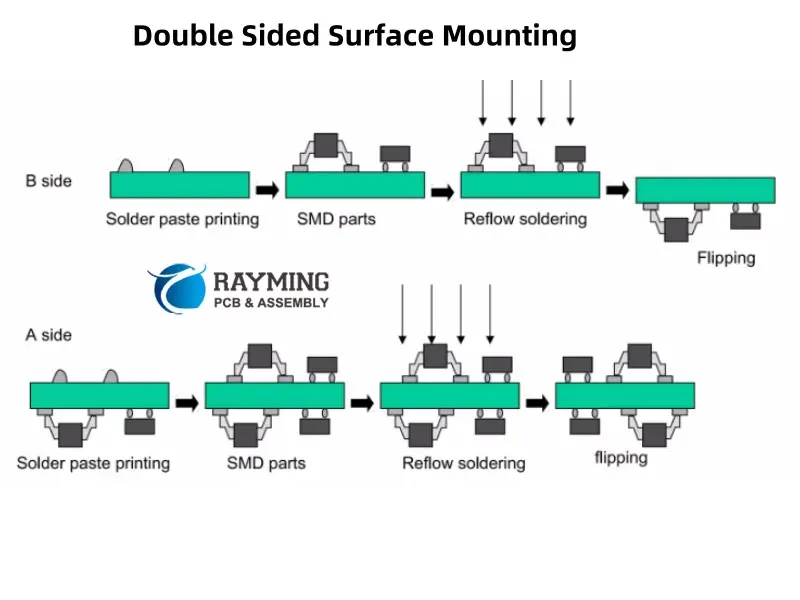
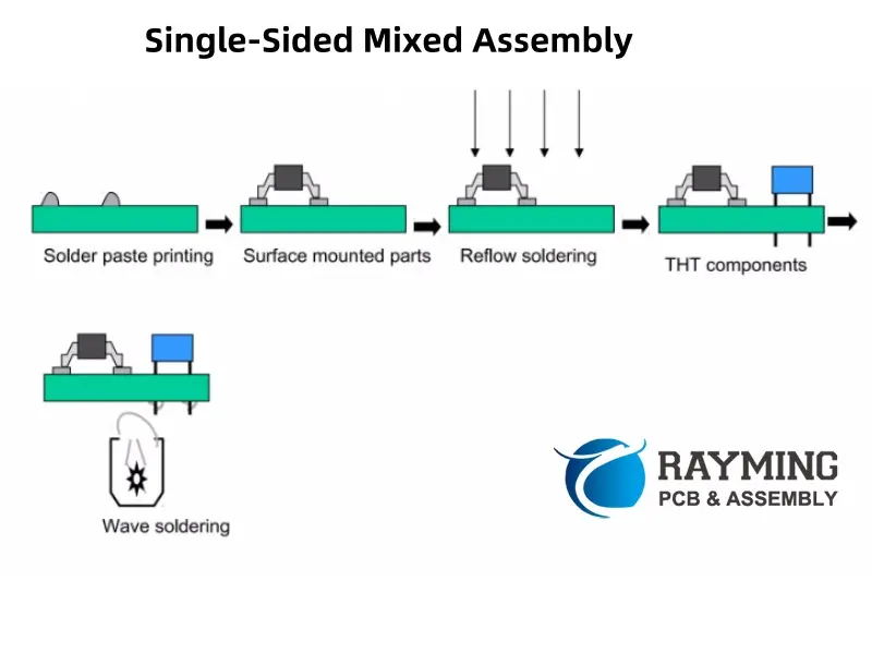
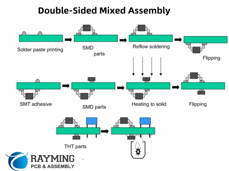
Techniques for Efficient PCB Assembly

Printed Circuit Board (PCB) assembly is often the core of Electronic Device Assembly. To optimize this process:

  1. Optimize Component Placement: Arrange components for efficient soldering and testing.
  2. Use Solder Paste Stencils: Ensure consistent solder application.
  3. Implement Reflow Soldering: For high-volume production of surface-mount components.
  4. Utilize Wave Soldering: For through-hole components in large-scale production.

Standardization and Modular Design Benefits

Adopting standardized processes and modular design principles can significantly enhance efficiency:

  • Repeatable Processes: Standardization ensures consistency across production runs.
  • Easier Training: New staff can learn standardized procedures more quickly.
  • Simplified Troubleshooting: Modular designs make it easier to isolate and fix issues.
  • Flexibility: Modular components can be easily updated or replaced.

ESD Protection Methods

Electrostatic Discharge (ESD) can damage sensitive electronic components. Implement these protection methods:

  • ESD Mats and Wrist Straps: Keep operators grounded while working.
  • Ionizers: Neutralize static charges in the air.
  • ESD-Safe Packaging: Protect components during storage and transport.
  • Regular Testing: Conduct periodic checks of ESD protection equipment.

Quality Assurance and Testing

Importance of In-Process Testing During Assembly

Integrating testing throughout the assembly process helps catch issues early:

  • Reduces Rework: Identifying problems immediately saves time and resources.
  • Improves Yield: Continuous testing leads to higher percentages of successful assemblies.
  • Enables Process Improvement: Data from in-process testing can highlight areas for optimization.

Final Product Inspection Best Practices

Before shipping, conduct thorough final inspections:

  1. Visual Inspection: Check for physical defects or misaligned components.
  2. Functional Testing: Ensure the device performs all intended functions.
  3. Stress Testing: Subject devices to simulated real-world conditions.
  4. Batch Sampling: For large production runs, test a representative sample.

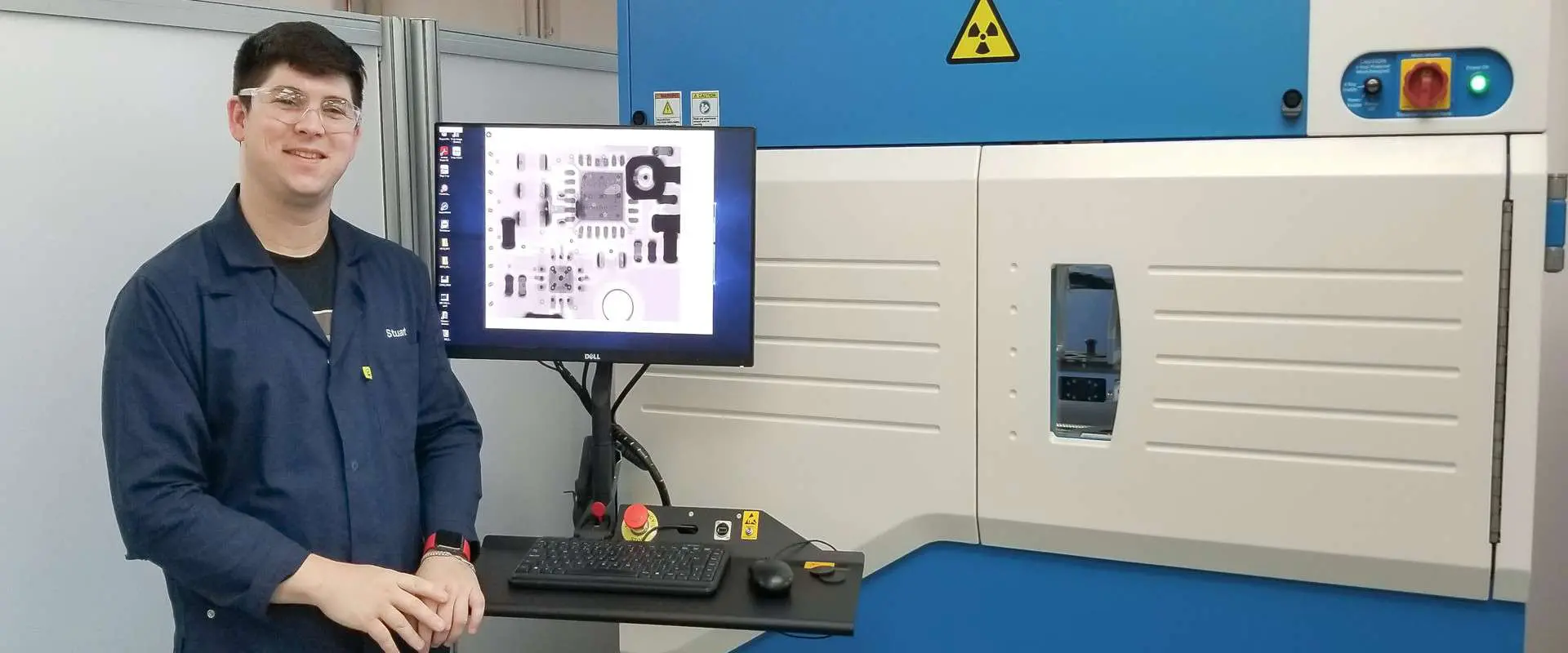
Common Testing Tools

Equip your quality assurance team with these essential tools:

  • Multimeters: For measuring voltage, current, and resistance.
  • Oscilloscopes: To analyze electrical signals and waveforms.
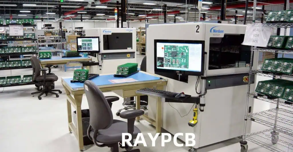
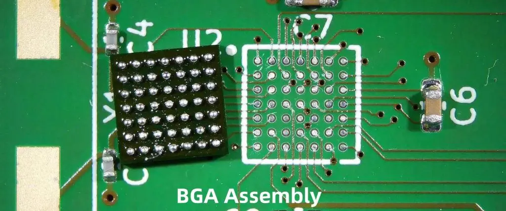
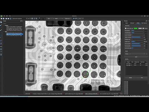
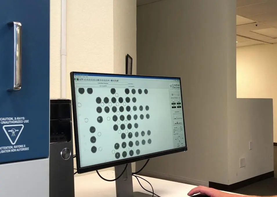
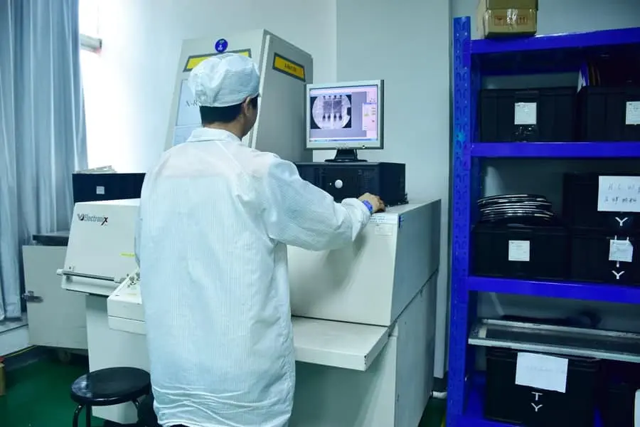
  • X-ray Inspection Systems: For examining internal components and solder joints.
  • Automated Optical Inspection (AOI) Machines: For high-speed, detailed visual inspections.

Streamlining the Assembly Line

Lean Manufacturing Principles in Electronic Device Assembly

Applying lean principles can significantly improve efficiency:

  • Value Stream Mapping: Identify and eliminate non-value-adding activities.
  • Just-in-Time Production: Minimize inventory and reduce waste.
  • Continuous Flow: Design the assembly line for smooth, uninterrupted production.
  • Pull Systems: Produce based on actual demand rather than forecasts.

Workflow Optimization Tips

  1. Analyze Current Processes: Identify bottlenecks and inefficiencies.
  2. Reorganize Workstations: Arrange tools and components for optimal flow.
  3. Implement Visual Management: Use clear signage and color-coding for quick identification.
  4. Encourage Employee Feedback: Front-line workers often have valuable insights for improvement.

Importance of Employee Training and Continuous Improvement

Invest in your workforce to drive efficiency:

  • Regular Training Sessions: Keep staff updated on best practices and new technologies.
  • Cross-Training: Enable employees to perform multiple tasks for increased flexibility.
  • Continuous Improvement Culture: Encourage employees to suggest and implement improvements.
  • Performance Metrics: Set clear goals and track progress to motivate continuous enhancement.

Sustainability in Electronic Device Assembly

Reducing Waste During Production

Implementing sustainable practices not only benefits the environment but can also improve efficiency:

  • Optimize Material Usage: Minimize scrap through precise cutting and efficient design.
  • Implement Recycling Programs: Properly dispose of and recycle electronic waste.
  • Reduce Packaging: Use minimal, recyclable packaging materials.
  • Energy-Efficient Equipment: Invest in machinery with lower power consumption.

Eco-Friendly Materials and Energy-Efficient Processes

Consider these sustainable options:

  • Lead-Free Solder: Comply with RoHS regulations and reduce environmental impact.
  • Biodegradable Components: Where possible, use materials that break down naturally.
  • Energy Recovery Systems: Capture and reuse heat generated during production.
  • Smart Lighting and HVAC: Implement systems that adjust based on occupancy and time of day.

Common Mistakes to Avoid

Inadequate Documentation

Poor documentation can lead to confusion and errors:

  • Incomplete Schematics: Ensure all designs are fully detailed and up-to-date.
  • Unclear Assembly Instructions: Provide step-by-step guides with clear visuals.
  • Lack of Version Control: Maintain a system to track changes and revisions.

Skipping Quality Checks

Rushing through quality assurance can result in costly recalls:

  • Insufficient Testing: Always perform thorough testing at each stage of assembly.
  • Ignoring Minor Issues: Small problems can escalate into major defects.
  • Lack of Final Inspection: Never skip the final quality check before shipping.

Poor Inventory Management

Inefficient inventory practices can disrupt production:

  • Overstocking: Ties up capital and increases storage costs.
  • Understocking: Leads to production delays and missed deadlines.
  • Poor Organization: Makes it difficult to locate necessary components quickly.

Future Trends in Electronic Device Assembly

Smart Factories and Industry 4.0

The future of Electronic Device Assembly is increasingly digital:

  • Internet of Things (IoT) Integration: Connected devices for real-time monitoring and adjustment.
  • Data Analytics: Using big data to predict maintenance needs and optimize processes.
  • Augmented Reality: AR tools for assembly guidance and training.

Impact of AI and Machine Learning on Device Assembly

Artificial Intelligence is revolutionizing assembly processes:

  • Predictive Maintenance: AI algorithms can forecast equipment failures before they occur.
  • Quality Control: Machine learning models can detect defects with superhuman accuracy.
  • Process Optimization: AI can analyze production data to suggest efficiency improvements.

Emerging Materials and Technologies

Stay ahead of the curve by exploring:

  • Nanotechnology: For creating smaller, more efficient components.
  • 3D Printing: For rapid prototyping and custom component production.
  • Flexible Electronics: Enabling new form factors and applications.

Conclusion

Efficient Electronic Device Assembly is crucial in today’s competitive electronics market. By implementing the best practices outlined in this guide, manufacturers can:

  • Improve product quality
  • Reduce production costs
  • Increase output and meet demand
  • Minimize environmental impact

The key to success lies in continuous evaluation and adaptation of assembly processes. As technology evolves, so too must the methods used to bring electronic devices to life. By staying informed about industry trends and consistently seeking ways to optimize operations, manufacturers can ensure they remain at the forefront of electronic device production.

Remember, efficiency in Electronic Device Assembly is not a destination but a journey of continuous improvement. Embrace new technologies, invest in your workforce, and always strive for excellence in every aspect of the assembly process.

FAQ

What is Electronic Device Assembly?

Electronic Device Assembly is the process of putting together various electronic components to create functional devices. This includes everything from simple circuit boards to complex smartphones and computers. The process involves several stages, including design, component sourcing, assembly, and testing.

How can you improve efficiency in Electronic Device Assembly?

To improve efficiency in Electronic Device Assembly:

  1. Implement lean manufacturing principles
  2. Invest in automation where appropriate
  3. Provide thorough training for assembly staff
  4. Use standardized processes and modular design
  5. Conduct regular quality checks throughout the assembly process
  6. Optimize your supply chain and inventory management
  7. Stay updated with the latest assembly technologies and techniques

What tools are essential for Electronic Device Assembly?

Essential tools for Electronic Device Assembly include:

  1. Soldering stations
  2. Pick-and-place machines for PCB assembly
  3. Microscopes and magnifying glasses for detailed work
  4. Multimeters and oscilloscopes for testing
  5. ESD protection equipment
  6. Automated optical inspection (AOI) systems
  7. X-ray inspection machines for checking internal components
  8. Reflow ovens for surface-mount technology (SMT) assembly

Remember, the specific tools required may vary depending on the complexity and scale of your assembly operations.

Best Rework Stations for Electronics Repair โ€“ 2025 Reviews & Buyer’s Guide

Rework Station

A rework station is a tool that enables easy desoldering and adjustment. Also, rework stations are de-soldering stations. The soldering function of these stations enables operators to use metal solder to repair metal. Rework refers to the repair of anย electronic circuitย board. It usually involves re-soldering and desoldering of surface mount devices. Therefore, rework stations are tools used to perform re-soldering and desoldering.

This comprehensive guide will walk you through the best rework stations available in 2025, their key features, and how to choose the right one for your specific requirements. We’ll explore various types of rework stations, from hot air systems to hybrid models, and provide in-depth reviews of the top performers in the market. By the end of this article, you’ll be equipped with the knowledge to make an informed decision on your next rework station purchase.

Types of Rework Stations

Understanding the different types of rework stations is crucial in selecting the right tool for your needs. Let’s explore the main categories:

1. Hot Air Rework Stations

Hot air rework stations use a stream of heated air to melt solder, making them ideal for surface-mount device (SMD) work.

Pros:

  • Excellent for SMD components
  • Non-contact heat application
  • Versatile temperature and airflow control

Cons:

  • May not be suitable for through-hole components
  • Can potentially damage heat-sensitive components if not used carefully

2. Soldering & Desoldering Stations

These stations combine soldering and desoldering capabilities in one unit, often with interchangeable tips.

Pros:

  • All-in-one solution for through-hole work
  • Precise temperature control
  • Efficient for both soldering and desoldering tasks

Cons:

  • May lack hot air functionality for SMD work
  • Can be more expensive than single-function stations

3. Hybrid Rework Stations

Hybrid stations combine hot air, soldering, and desoldering functions in a single unit.

Pros:

  • Versatile for all types of electronic repair work
  • Space-saving all-in-one solution
  • Cost-effective compared to buying separate tools

Cons:

  • Can be complex to operate for beginners
  • May compromise on specialized features found in dedicated stations

4. Infrared (IR) Rework Stations

IR stations use infrared heat to reflow solder, offering a more controlled and localized heating process.

Pros:

  • Precise and localized heating
  • Reduced risk of thermal damage to surrounding components
  • Ideal for working with sensitive or densely packed PCBs

Cons:

  • Generally more expensive than other types
  • May require a learning curve to use effectively

5. Manual vs. Automated Rework Stations

Manual stations require user operation, while automated stations can perform some tasks with minimal human intervention.

Manual Stations:

  • More affordable
  • Greater user control
  • Suitable for varied repair tasks

Automated Stations:

  • Higher precision and consistency
  • Increased efficiency for repetitive tasks
  • Often include advanced features like component placement

Read more about:

Key Features to Consider

When selecting a rework station, several key features should be taken into account:

1. Temperature Control

Precise temperature control is crucial for effective and safe rework. Look for:

  • Wide temperature range (typically 200ยฐC to 480ยฐC)
  • Digital temperature display
  • Quick heating and cooling capabilities
  • Temperature stability and accuracy (ยฑ5ยฐC or better)

2. Airflow Control

For hot air stations, airflow control is essential:

  • Adjustable airflow settings
  • Digital airflow display
  • Compatibility with various nozzle sizes

3. Power & Wattage

Higher wattage generally means faster heating and better temperature stability:

  • 60W to 100W for basic soldering stations
  • 100W to 300W for advanced rework stations
  • Consider power efficiency and energy-saving features

4. Build Quality & Ergonomics

A well-built station ensures longevity and comfort during use:

  • Durable materials (e.g., metal casing, heat-resistant plastics)
  • Comfortable handpieces with ergonomic design
  • Stable base with anti-slip features
  • Easy-to-read displays and intuitive controls

5. Safety Features

Prioritize safety with features like:

  • Auto sleep and shut-off functions
  • Password protection for settings
  • ESD (Electrostatic Discharge) safe design
  • Tip cleaning and storage options

6. Compatibility

Ensure the station is compatible with your needs:

  • Variety of available tips and nozzles
  • Compatibility with different solder types
  • Adaptability for future upgrades or accessories

7. Brand Reputation & Warranty

Choose reputable brands that offer:

  • Reliable customer support
  • Comprehensive warranty coverage
  • Availability of replacement parts and accessories

Top 5 Best Rework Stations of 2025

bga rework process

1. Hakko FR-301 Desoldering Tool

The Hakko FR-301 continues to be a top choice for professionals in 2025, known for its exceptional desoldering capabilities.

Key Features:

  • Powerful vacuum pump for efficient solder removal
  • Compact and portable design
  • Easy-to-clean solder collection chamber
  • Ceramic heating element for long-lasting performance

Pros:

  • Excellent build quality and reliability
  • Quick heat-up time and temperature stability
  • Ergonomic design for comfortable extended use

Cons:

  • Focused primarily on desoldering tasks
  • Higher price point compared to multi-function stations

2. Quick 861DW Hot Air Rework Station

The Quick 861DW stands out in 2025 as a versatile hot air station suitable for both professionals and advanced hobbyists.

Key Features:

  • Wide temperature range (100ยฐC to 500ยฐC)
  • Digital display with precise temperature and airflow control
  • Auto-sleep and cool-down functions
  • Brushless fan for quiet operation and longevity

Pros:

  • Excellent temperature stability and accuracy
  • User-friendly interface with programmable presets
  • Comprehensive set of nozzles included

Cons:

  • Lacks built-in soldering functionality
  • May be overkill for occasional users

3. YIHUA 959D Hybrid Soldering & Hot Air Station

The YIHUA 959D offers a cost-effective solution for those needing both soldering and hot air capabilities in 2025.

Key Features:

  • 3-in-1 functionality: soldering iron, hot air gun, and smoke absorber
  • Dual digital displays for temperature control
  • ESD safe design
  • Comprehensive accessory kit included

Pros:

  • Versatile functionality at an affordable price point
  • Suitable for both through-hole and SMD work
  • Compact design ideal for smaller workspaces

Cons:

  • May lack some advanced features of higher-end models
  • Build quality may not match premium brands

4. JBC CD-2BE Soldering & Desoldering Station

JBC’s CD-2BE represents the high-end market in 2025, offering professional-grade soldering and desoldering capabilities.

Key Features:

  • Advanced temperature control with sleep and hibernation modes
  • Intelligent heat management system
  • USB connectivity for software updates and data logging
  • Modular design for easy maintenance and upgrades

Pros:

  • Exceptional temperature stability and recovery time
  • High-quality construction built to last
  • Ergonomic handpieces with quick-change cartridge system

Cons:

  • Premium price point
  • Steep learning curve to utilize all features

5. Aoyue Int968A+ All-in-One Rework Station

The Aoyue Int968A+ stands out in 2025 as a comprehensive solution for various rework needs.

Key Features:

  • Combines hot air, soldering iron, and smoke absorption
  • Built-in component tester and power supply
  • Large LCD display with intuitive controls
  • Extensive range of included accessories

Pros:

  • All-in-one solution for diverse repair tasks
  • Good value for the range of features offered
  • Suitable for both beginners and experienced users

Cons:

  • Jack-of-all-trades approach may compromise on specialized tasks
  • Bulkier than single-function stations

Buyer’s Guide โ€“ How to Choose the Right Rework Station

bga-rework-machine

1. Assess Your Needs

Consider the following:

  • Types of components you work with most often
  • Frequency and intensity of use
  • Required precision level
  • Available workspace

2. Budget Considerations

Rework stations can range from under 100toover100toover1000:

  • Entry-level:ย 50โˆ’50โˆ’200 (suitable for hobbyists and occasional use)
  • Mid-range:ย 200โˆ’200โˆ’500 (good for regular use and small businesses)
  • Professional: $500+ (ideal for heavy-duty, professional use)

3. Future-Proofing

Look for:

  • Modular designs that allow for upgrades
  • Compatibility with a wide range of accessories
  • Software updateability (for digital models)

4. User Reviews & Recommendations

  • Read reviews from verified purchasers
  • Seek recommendations from industry forums and communities
  • Consider professional reviews and comparisons

5. Where to Buy

  • Authorized dealers and distributors
  • Reputable online retailers (e.g., DigiKey, Mouser, Amazon)
  • Direct from manufacturers (often for higher-end models)

Soldering Station Vs. Rework Station

While often used interchangeably, there are key differences:

Soldering Station:

  • Primarily for soldering tasks
  • Usually includes a soldering iron and temperature control unit
  • May include basic desoldering capabilities

Rework Station:

  • More comprehensive, often including hot air functionality
  • Designed for both soldering and desoldering tasks
  • May include additional features like component testers or fume extraction

Choose based on your primary needs: soldering stations for mainly through-hole work, rework stations for more diverse tasks including SMD work.

Common Rework Station FAQs

  1. Q: How often should I clean my rework station? A: Clean after each use, with a deep clean every 40-50 hours of operation.
  2. Q: Can I use lead-free solder with any rework station? A: Most modern stations are compatible, but check the manufacturer’s specifications.
  3. Q: What’s the ideal temperature for SMD rework? A: Typically between 300ยฐC to 350ยฐC, but always consult component specifications.
  4. Q: How long do heating elements in rework stations typically last? A: With proper care, 2-5 years for heavy use, longer for occasional use.
  5. Q: Is ESD protection necessary for all rework stations? A: It’s highly recommended to prevent damage to sensitive components.
  6. Q: Can I use a rework station for tasks other than electronics repair? A: While possible, it’s not recommended as it may damage the station or void warranties.
  7. Q: How important is brand name when choosing a rework station? A: Reputable brands often offer better quality, support, and longevity, but there are good options across price ranges.

In conclusion, choosing the right rework station in 2025 involves carefully considering your specific needs, budget, and the features offered by various models. Whether you opt for a specialized desoldering tool like the Hakko FR-301 or an all-in-one solution like the Aoyue Int968A+, ensure that your choice aligns with your work requirements and skill level. Remember to prioritize safety features, build quality, and long-term value when making your decision. With the right rework station, you’ll be well-equipped to tackle a wide range of electronics

Step-by-Step BGA Reballing Process to Solve SMT Soldering Failures

BGA Reballing

Introduction

Ball Grid Array (BGA) technology has become an indispensable part of creating compact, high-performance devices. However, with the increasing complexity of electronic components, BGA failures have emerged as a significant challenge in Surface Mount Technology (SMT) soldering processes. This comprehensive guide will walk you through the intricate process of BGA reballing, a crucial technique used to address SMT soldering failures and restore functionality to faulty components.

What Is BGA Reballing?

BGA reballing is a specialized repair technique used in electronics manufacturing to replace the solder balls on a BGA component. These tiny spheres of solder serve as the connection points between the BGA chip and the printed circuit board (PCB). When these connections fail due to various factors, reballing becomes necessary to restore the component’s functionality.

The process involves carefully removing the old solder balls, thoroughly cleaning the BGA component, and then precisely placing new solder balls in their correct positions. This delicate procedure requires a combination of skill, patience, and specialized equipment, particularly a BGA rework station, to ensure success.

Why Is BGA Reballing Needed?

Understanding the reasons behind BGA reballing is crucial for electronics manufacturers and repair technicians. Let’s explore the primary causes of BGA failure and the signs that indicate a need for reballing.

Causes of BGA Failure

  1. Thermal stress: Repeated heating and cooling cycles can cause solder joints to crack or separate over time.
  2. Manufacturing defects: Poor soldering during the initial assembly process can lead to weak or incomplete connections.
  3. Physical damage: Drops, impacts, or excessive vibration can break solder connections or damage the BGA package.
  4. Environmental factors: Exposure to extreme temperatures, humidity, or corrosive environments can accelerate solder joint degradation.
  5. Electromigration: High current densities can cause solder material to migrate, weakening connections over time.
  6. Warpage: PCB or BGA substrate warpage can lead to uneven solder connections or complete separation of joints.

Signs a BGA Needs Reballing

Identifying when a BGA component requires reballing is essential for maintaining the integrity and functionality of electronic devices. Common indicators include:

  1. Intermittent device functionality or performance issues
  2. No display or distorted video output in devices with graphics processors
  3. Boot failures or system crashes in computing devices
  4. Overheating of specific areas on the PCB near the BGA component
  5. Visual inspection revealing cracked, missing, or deformed solder balls
  6. X-ray analysis showing voids, bridges, or inconsistencies in solder connections
  7. Failure to pass electrical continuity tests between the BGA and PCB
YouTube video

Tools & Supplies for BGA Reballing

To successfully perform BGA reballing, you’ll need a set of specialized tools and supplies. The cornerstone of this process is a high-quality BGA rework station, which provides precise temperature control and hot air capabilities. Here’s a comprehensive list of essential items:

Essential Tools List:

  1. BGA rework station: The primary tool for the reballing process, featuring accurate temperature control and hot air functionality.
  2. Reflow oven or hot air station: For controlled heating during the reballing process.
  3. Solder paste flux (water-soluble preferred): Aids in the proper flow and adhesion of solder.
  4. Soldering iron with a blade tip: For precise removal of old solder and cleanup.
  5. Solder braid or wick: To remove excess solder during the cleaning process.
  6. Preformed solder balls: Sized to match the BGA component’s specifications.
  7. ESD-safe workspace: Including a wrist strap and anti-static mat to prevent electrostatic discharge.
  8. Inspection tools: High-magnification microscope and X-ray machine for quality control.
  9. Cleaning supplies: Isopropyl alcohol, lint-free cloths, and specialized PCB cleaners.
  10. Tweezers and handling tools: For precise placement of solder balls.
  11. Stencils or templates: To ensure accurate alignment of new solder balls.
  12. Heat-resistant tape: For masking surrounding areas during the reballing process.
  13. Thermal camera: To monitor temperature distribution during reflow.

Having these tools at your disposal, particularly a reliable BGA rework station, will significantly increase your chances of successful BGA reballing.

Read more about:

Step-by-Step BGA Reballing Process

BGA Rework Services

Now, let’s dive into the detailed process of BGA reballing, focusing on the use of a BGA rework station throughout the procedure.

Step 1: Component Removal from the PCB

The first step in the BGA reballing process is to carefully remove the faulty component from the PCB:

  1. Preheat the PCB using your BGA rework station to reduce thermal shock.
  2. Use the hot air nozzle of the rework station to evenly heat the BGA component.
  3. Monitor the temperature using the station’s built-in sensors or a thermal camera.
  4. Once the solder reaches its melting point, gently lift the component using vacuum pickup tools.
  5. Place the removed component on an ESD-safe surface for further processing.

Step 2: Deballing

Deballing involves removing the old solder balls from the BGA component:

  1. Apply a thin layer of flux to the solder balls to aid in removal.
  2. Use your BGA rework station’s hot air to heat the component evenly.
  3. Once the solder melts, carefully separate the component from the old solder balls.
  4. Use solder wick and your soldering iron to remove any remaining solder from the pads.

Step 3: Inspection Post Deballing

After deballing, thorough inspection is crucial:

  1. Use a high-magnification microscope to examine the BGA pads.
  2. Look for any signs of damage, lifted pads, or residual solder.
  3. Clean any flux residue for a clear view of the pads.
  4. Document any irregularities for future reference.

Step 4: Moisture Removal-Post Deball

Moisture can significantly impact the reballing process:

  1. Use your BGA rework station’s built-in oven or a separate baking oven.
  2. Bake the BGA component at 125ยฐC for 4-6 hours.
  3. This step removes any absorbed moisture, preventing issues during reflow.

Step 5: Clean the Deballed Part

Proper cleaning ensures optimal adhesion of new solder balls:

  1. Use isopropyl alcohol and lint-free cloths to clean the BGA pads.
  2. For stubborn residues, use specialized PCB cleaners.
  3. Ensure all flux and contaminants are completely removed.
  4. Use your BGA rework station’s hot air at a low temperature to dry the component thoroughly.

Step 6: Drying Post Re-ball

After cleaning, it’s essential to dry the component thoroughly:

  1. Use your BGA rework station’s hot plate or a separate low-temperature oven.
  2. Maintain a temperature of about 80ยฐC for 30 minutes.
  3. This step evaporates any remaining cleaning solvents.

Step 7: Baking to Remove Moisture Post Re-ball

Another baking cycle helps ensure the component is completely moisture-free:

  1. Use your BGA rework station’s oven feature or a separate baking oven.
  2. Bake the cleaned and dried component at 125ยฐC for 4-6 hours.
  3. This step is crucial for preventing moisture-related issues during reflow.

Step 8: Apply Paste Flux

Flux application is critical for proper solder ball adhesion:

  1. Use a stencil or manual application method to apply a thin, even layer of flux to the BGA pads.
  2. Ensure all pads are covered, but avoid excess flux that could cause bridging.
  3. Your BGA rework station’s magnification feature can help ensure even application.

Step 9: Attach Pre-formed Solder Balls

This step requires precision and patience:

  1. Use a ball placement stencil aligned with the BGA pads.
  2. Carefully place pre-formed solder balls into each hole in the stencil.
  3. Gently remove the stencil, leaving the solder balls in position on the flux.
  4. Use your BGA rework station’s magnification to verify correct placement.

Step 10: BGA Component Placement

Proper placement is crucial for successful reballing:

  1. Use your BGA rework station to preheat the component according to the manufacturer’s specifications.
  2. Follow the machine’s specific profile for your component type.
  3. Monitor the reflow process using the station’s thermal sensors or a separate thermal camera.
  4. Allow the component to cool naturally to avoid thermal stress.

Step 11: Inspection

Post-reflow inspection is vital to ensure quality:

  1. Use X-ray inspection to check for voids, bridges, or misaligned balls.
  2. Perform a visual inspection under a microscope for any obvious defects.
  3. If issues are found, the process may need to be repeated from Step 2.

Step 12: Reassembly & Testing

The final step involves reattaching the component and verifying functionality:

  1. Clean the PCB area where the BGA will be attached.
  2. Apply flux to the PCB pads.
  3. Carefully align and place the reballed BGA component.
  4. Use your BGA rework station to reflow the BGA onto the PCB, following the appropriate temperature profile.
  5. After cooling, perform functional tests to ensure the repair was successful.

Advanced Techniques & Quality Control

Moisture Prevention

Moisture control is critical throughout the reballing process:

  1. Use dry storage containers for components awaiting reballing.
  2. Implement humidity-controlled workspaces.
  3. Minimize exposure time between baking and reballing steps.
  4. Consider using nitrogen purge systems in your BGA rework station for an inert environment.

Automation

For high-volume operations, consider automated solutions:

  1. Automatic ball placement machines increase accuracy and speed.
  2. Robotic handling systems reduce human error and contamination risks.
  3. Automated optical inspection (AOI) systems for consistent quality control.
  4. Advanced BGA rework stations with programmable profiles for repeatable results.

X-Ray Inspection

X-ray technology is invaluable for BGA quality assurance:

  1. Use X-ray systems to inspect hidden solder joints.
  2. Look for voids, bridges, and misalignments that are invisible to the naked eye.
  3. Implement regular X-ray inspections as part of your quality control process.
  4. Consider investing in a BGA rework station with built-in X-ray capabilities for seamless integration.

BGA Reballing Services vs. DIY

bga-reballing-station

When faced with BGA failures, you have two main options: professional reballing services or doing it yourself (DIY).

Professional BGA Reballing Services

Pros:

  • Access to high-end equipment and expertise
  • Consistent results with high success rates
  • Time-saving for businesses with limited resources
  • Often comes with warranties or guarantees

Cons:

  • Can be expensive, especially for low volumes
  • Turnaround time may not suit urgent needs
  • Less control over the process

DIY BGA Reballing

Pros:

  • Cost-effective for frequent repairs
  • Immediate turnaround time
  • Complete control over the process
  • Opportunity to develop in-house expertise

Cons:

  • Requires significant investment in equipment, particularly a quality BGA rework station
  • Steep learning curve and potential for errors
  • Time-consuming, especially for beginners
  • May void warranties on certain components

The choice between professional services and DIY depends on your specific needs, volume of repairs, available resources, and in-house expertise. If you decide to go the DIY route, investing in a high-quality BGA rework station is crucial for achieving professional-level results.

Conclusion

BGA reballing is a complex yet essential process in the world of electronics repair and manufacturing. By following this comprehensive guide and utilizing a professional-grade BGA rework station, you can navigate the intricacies of BGA reballing with confidence. Remember that practice, patience, and the right equipment are key to mastering this technique.

As technology continues to advance, the importance of skilled BGA reballing will only grow. Whether you choose to invest in developing in-house capabilities or rely on professional services, understanding the process is crucial for anyone involved in electronics manufacturing or repair.

By implementing proper techniques, investing in quality equipment like a reliable BGA rework station, and maintaining rigorous quality control, you can successfully address SMT soldering failures and extend the life of valuable electronic components. The ability to perform successful BGA reballing not only saves costs but also contributes to reducing electronic waste, aligning with global sustainability efforts.

Stay updated with the latest advancements in BGA technology, rework stations, and reballing techniques to ensure you’re always at the forefront of electronics repair and manufacturing. With the knowledge gained from this guide and the right tools at your disposal, you’re well-equipped to tackle BGA-related challenges and maintain the reliability of your electronic products.

12 Reliable PCB Assembly Houses in Austria

PCB assembly house in Austria

In today’s rapidly evolving electronics industry, choosing the right PCB assembly house is crucial for the success of any project. Austria, with its growing electronics and manufacturing sector, has become a hub for high-quality PCB assembly services. This article presents a curated list of the top 12 PCB assembly houses in Austria, selected based on their quality, services, and reputation. Whether you’re a startup or an established company, finding the perfect partner for your PCB assembly needs has never been easier.

What is a PCB Assembly House?

Before diving into our list, let’s understand what a PCB assembly house does and why it’s essential to partner with a reliable one.

Definition and Role

A PCB assembly house is a specialized facility that assembles electronic components onto printed circuit boards (PCBs). These houses play a crucial role in turning design schematics into functional electronic products.

Key Services Offered

PCB assembly houses typically offer a range of services, including:

  1. Surface Mount Technology (SMT) assembly
  2. Through-hole component insertion
  3. Prototyping
  4. Testing and quality assurance
  5. Design for Manufacturing (DFM) review
  6. Component sourcing and procurement

Importance of a Reliable Partner

Partnering with a dependable PCB assembly house ensures:

  • Consistent quality in your electronic products
  • Faster time-to-market
  • Cost-effective production
  • Access to cutting-edge technology and expertise

Criteria for Selection

When compiling our list of top PCB assembly houses in Austria, we considered several crucial factors:

Quality Standards and Certifications

We looked for companies with:

  • ISO 9001 certification for quality management
  • IPC standards compliance
  • RoHS compliance for environmental responsibility

Range of Services

The best PCB assembly houses offer comprehensive services, from prototype to full production runs.

Lead Time and Delivery Capabilities

We considered companies with efficient production processes and reliable delivery times.

Customer Reviews and Industry Reputation

Feedback from clients and standing within the industry played a significant role in our selection.

Technological Capabilities

We favored companies with modern machinery and advanced technologies like AI-assisted inspection systems.

Read more about:

Top 12 PCB Assembly Houses in Austria

Now, let’s explore the cream of the crop when it comes to PCB assembly in Austria.

1. AlpineCircuits GmbH

Overview

AlpineCircuits GmbH is a leading PCB assembly house known for its precision and cutting-edge technology.

Specialties and Services

  • High-density interconnect (HDI) PCB assembly
  • Flex and rigid-flex PCB assembly
  • Prototype to high-volume production

Certifications

  • ISO 9001:2015
  • IPC-A-610 Class 3
  • AS9100D (Aerospace standard)

Industries Served

  • Aerospace
  • Medical devices
  • Telecommunications

Visit AlpineCircuits GmbH

2. TechnoAlp Electronics

Overview

TechnoAlp Electronics specializes in rapid prototyping and small to medium production runs.

Specialties and Services

  • 24-hour prototype service
  • Mixed technology assembly
  • In-circuit and functional testing

Certifications

  • ISO 9001:2015
  • IPC-A-610 Class 2

Industries Served

Visit TechnoAlp Electronics

3. Vienna Circuit Solutions

Overview

Vienna Circuit Solutions is renowned for its advanced SMT capabilities and high-volume production capacity.

Specialties and Services

  • Advanced SMT assembly
  • BGA and micro-BGA placement
  • Automated optical inspection (AOI)

Certifications

  • ISO 9001:2015
  • ISO 14001:2015 (Environmental management)
  • IPC-A-610 Class 3

Industries Served

  • Telecommunications
  • Military and defense
  • Renewable energy

Visit Vienna Circuit Solutions

4. GrazTech PCB Assembly

Overview

GrazTech PCB Assembly is known for its expertise in complex, multi-layer PCB assembly.

Specialties and Services

  • Multi-layer PCB assembly (up to 32 layers)
  • X-ray inspection for hidden solder joints
  • Conformal coating services

Certifications

  • ISO 9001:2015
  • IPC-A-610 Class 3
  • ISO 13485:2016 (Medical devices)

Industries Served

  • Medical technology
  • Aerospace
  • Scientific instruments

Visit GrazTech PCB Assembly

5. Innsbruck Electronics Manufacturing

Overview

Innsbruck Electronics Manufacturing specializes in low-volume, high-mix production runs.

Specialties and Services

  • Flexible production lines for varied batch sizes
  • Hand assembly for complex or delicate components
  • Full box build and system integration

Certifications

  • ISO 9001:2015
  • IPC-A-610 Class 2

Industries Served

  • Industrial controls
  • Automotive prototyping
  • IoT devices

Visit Innsbruck Electronics Manufacturing

6. Salzburg Precision Circuits

Overview

Salzburg Precision Circuits is acclaimed for its high-precision assembly of fine-pitch components.

Specialties and Services

  • Ultra-fine pitch component placement (down to 0201)
  • Lead-free and leaded soldering options
  • Flying probe testing

Certifications

  • ISO 9001:2015
  • IPC-A-610 Class 3
  • IATF 16949:2016 (Automotive quality management)

Industries Served

  • Automotive electronics
  • Medical implants
  • High-frequency communications

Visit Salzburg Precision Circuits

7. LinzTronic Assembly Solutions

Overview

LinzTronic Assembly Solutions offers a full suite of PCB assembly services with a focus on Industry 4.0 integration.

Specialties and Services

  • Automated component placement and soldering
  • Real-time production monitoring
  • Supply chain management and kitting services

Certifications

  • ISO 9001:2015
  • ISO 14001:2015
  • IPC-A-610 Class 3

Industries Served

  • Smart home devices
  • Industrial IoT
  • Electric vehicle components

Visit LinzTronic Assembly Solutions

8. Klagenfurt Circuit Builders

Overview

Klagenfurt Circuit Builders specializes in quick-turn prototyping and small production runs.

Specialties and Services

Certifications

  • ISO 9001:2015
  • IPC-A-610 Class 2

Industries Served

  • Consumer electronics
  • Wearable technology
  • Educational electronics

Visit Klagenfurt Circuit Builders

9. Vorarlberg Advanced Electronics

Overview

Vorarlberg Advanced Electronics is known for its advanced testing capabilities and quality assurance processes.

Specialties and Services

  • In-circuit testing (ICT)
  • Boundary scan testing
  • Environmental stress screening

Certifications

  • ISO 9001:2015
  • AS9100D
  • IPC-A-610 Class 3

Industries Served

  • Aerospace and defense
  • Industrial controls
  • High-reliability computing

Visit Vorarlberg Advanced Electronics

10. St. Pรถlten Micro Assembly

Overview

St. Pรถlten Micro Assembly specializes in microelectronics and advanced packaging technologies.

Specialties and Services

  • Chip-on-board (COB) assembly
  • Flip chip bonding
  • Microwave and RF circuit assembly

Certifications

  • ISO 9001:2015
  • ISO 13485:2016
  • IPC-A-610 Class 3

Industries Served

  • Telecommunications
  • Medical diagnostics
  • Satellite communications

Visit St. Pรถlten Micro Assembly

11. Eisenstadt Circuit Technologies

Overview

Eisenstadt Circuit Technologies offers a blend of traditional and cutting-edge PCB assembly services.

Specialties and Services

  • Mixed-technology assembly (SMT and through-hole)
  • Selective soldering
  • Conformal coating and potting

Certifications

  • ISO 9001:2015
  • IPC-A-610 Class 2
  • UL approval for specific processes

Industries Served

  • Renewable energy systems
  • Building automation
  • Transportation systems

Visit Eisenstadt Circuit Technologies

12. Bregenz Precision Electronics

Overview

Bregenz Precision Electronics is renowned for its high-mix, low-volume production capabilities.

Specialties and Services

  • Flexible production lines
  • Box build and final assembly
  • Functional testing and burn-in services

Certifications

  • ISO 9001:2015
  • ISO 14001:2015
  • IPC-A-610 Class 3

Industries Served

  • Scientific instruments
  • Medical devices
  • Industrial automation

Visit Bregenz Precision Electronics

Benefits of Choosing an Austrian PCB Assembly House

Opting for an Austrian PCB assembly house comes with several advantages:

High-Quality European Standards

Austrian companies adhere to strict European quality standards, ensuring top-notch products.

Geographic and Logistic Advantages

For EU-based companies, working with Austrian assemblers means shorter lead times and easier communication.

Innovation and Technology Leadership

Austria’s strong focus on R&D translates to cutting-edge assembly technologies and processes.

How to Choose the Right PCB Assembly House for Your Needs

To select the ideal PCB assembly partner:

Evaluation Checklist

  1. Assess their technical capabilities
  2. Review their quality certifications
  3. Check their industry experience
  4. Evaluate their communication and support
  5. Consider their pricing and lead times

Importance of Sample Orders and Audits

Always request sample runs and, if possible, conduct on-site audits before committing to large orders.

Conclusion

Austria boasts some of the best PCB assembly houses in Europe, combining precision engineering with cutting-edge technology. Whether you need rapid prototyping or high-volume production, these top 12 PCB assembly houses offer a range of services to meet your specific requirements. We encourage you to reach out to a few of these top choices for quotes and consultations to find the perfect partner for your PCB assembly needs.

FAQs

What is the average lead time for PCB assembly in Austria?

Lead times vary depending on complexity and volume, but typically range from 5-15 business days for standard orders. Rush services can often deliver in 2-3 days for an additional fee.

Are Austrian PCB assembly houses suitable for startups?

Absolutely! Many Austrian PCB assembly houses, like Klagenfurt Circuit Builders and TechnoAlp Electronics, specialize in prototype and low-volume runs, making them ideal partners for startups.

How much does PCB assembly typically cost in Austria?

Costs can vary widely based on complexity, volume, and components. However, you can expect prices to be competitive with other European countries, typically ranging from โ‚ฌ0.05 to โ‚ฌ0.50 per component placed for medium-volume runs.

Electronic Assembly at Home: PCB Soldering, Circuit Board Assembly & Work-from-Home Jobs

Electronic Assembly At Home

Electronic devices are an important part of present life since they have a wide range of applications. However, the existence of these devices solely depends on electronic assembly. For example, the manufacture of such appliances like refrigerators, smart cars, air conditioners, and many other machines depends on printed circuit boards (PCBs). Therefore, we will look at what electronic assembly at home is and dig deep into what it involves. In addition, we will highlight the advantages and disadvantages of assembling electronics at home.

What is Electronic Assembly at Home?

Understanding the Concept

Electronic Assembly at Home refers to the process of assembling, soldering, and testing electronic components and circuit boards in a residential setting. This practice has gained popularity due to advancements in technology, the rise of the maker movement, and the increasing demand for flexible work arrangements.

Typical Tasks Involved

When engaging in electronic assembly at home, you can expect to perform a variety of tasks, including:

  1. Soldering components onto printed circuit boards (PCBs)
  2. Mounting through-hole and surface-mount components
  3. Testing circuits and troubleshooting issues
  4. Reading and interpreting circuit schematics
  5. Assembling complete electronic devices or prototypes

Required Skills and Basic Knowledge

To excel in electronic assembly at home, you’ll need to develop the following skills and knowledge:

  • Basic understanding of electronic components and their functions
  • Proficiency in soldering techniques
  • Ability to read and interpret circuit diagrams
  • Familiarity with various types of PCBs and assembly methods
  • Knowledge of safety procedures and proper handling of electronic components
  • Attention to detail and patience for precise work

Essential Tools and Equipment for Home Electronic Assembly

Creating a well-equipped workspace is crucial for successful electronic assembly at home. Here are the essential tools and equipment you’ll need:

Soldering Irons and Stations

  • Temperature-controlled soldering iron
  • Soldering station with adjustable temperature settings
  • Various soldering tips for different applications

Multimeters and Circuit Testers

  • Digital multimeter for measuring voltage, current, and resistance
  • Continuity tester for checking connections
  • Logic probe for testing digital circuits

PCB Holders, Tweezers, and Magnifiers

  • PCB holder or vise for secure board positioning
  • Fine-tipped tweezers for handling small components
  • Magnifying glass or illuminated magnifier for detailed work

Safety Gear and Workbench Setup

  • Safety glasses to protect your eyes
  • Anti-static wrist strap to prevent electrostatic discharge
  • Fume extractor or well-ventilated workspace
  • ESD-safe work surface
  • Proper lighting for clear visibility

How to Solder PCBs at Home: A Beginner’s Guide

Soldering is a fundamental skill in electronic assembly. Follow these steps to master PCB soldering at home:

Preparing Your Workspace

  1. Set up your soldering station in a well-ventilated area
  2. Ensure proper lighting and a comfortable seating position
  3. Organize your components and tools for easy access

Selecting the Right Solder and Components

  1. Choose lead-free solder for environmental safety
  2. Select the appropriate solder diameter for your project
  3. Ensure you have all the necessary components before starting

Step-by-Step Soldering Instructions

  1. Clean the PCB and components with isopropyl alcohol
  2. Tin the soldering iron tip with a small amount of solder
  3. Heat both the component lead and the PCB pad simultaneously
  4. Apply solder to the junction, allowing it to flow smoothly
  5. Remove the iron and allow the solder joint to cool naturally

Common Soldering Mistakes and How to Avoid Them

  • Using too much solder, leading to bridges between connections
  • Insufficient heating, resulting in cold solder joints
  • Overheating components, causing damage or lifted pads
  • Poor tip maintenance, leading to inefficient heat transfer

Tips for Clean and Durable Connections

  • Keep your soldering iron tip clean and well-tinned
  • Use flux to improve solder flow and adhesion
  • Practice proper heat management to avoid damaging components
  • Inspect your work with a magnifying glass for quality assurance

Read more about:

Circuit Board Assembly at Home: Step-by-Step

Assembling complete circuit boards at home requires attention to detail and a systematic approach. Here’s a step-by-step guide:

Understanding Circuit Schematics

  1. Familiarize yourself with common schematic symbols
  2. Learn to trace signal paths and identify component connections
  3. Use software tools like KiCad or Eagle for schematic design and PCB layout

Placing Components (Through-Hole and Surface Mount)

  1. Start with larger components and work your way to smaller ones
  2. Use the PCB silkscreen as a guide for component placement
  3. Double-check component values and polarities before soldering

Soldering and Securing Components

  1. Begin with through-hole components, soldering from the bottom of the board
  2. For surface-mount components, apply solder paste and use a hot air rework station or reflow oven
  3. Ensure all connections are secure and free from solder bridges

Inspection and Troubleshooting

  1. Visually inspect all solder joints using a magnifying glass
  2. Use a multimeter to check for continuity and proper connections
  3. Power up the board and test functionality, addressing any issues that arise

Finding Work-from-Home Jobs in Electronic Assembly

The rise of remote work has created new opportunities in electronic assembly. Here’s how to find and secure work-from-home jobs in this field:

Companies Hiring for Remote Electronic Assembly

  • Research electronics manufacturers offering remote positions
  • Explore job boards specializing in electronics and engineering roles
  • Connect with staffing agencies focusing on technical and manufacturing jobs

Freelancing and Starting Your Own Service

  1. Create a portfolio showcasing your skills and completed projects
  2. Set up profiles on freelancing platforms like Upwork or Fiverr
  3. Network with local businesses and startups that may need prototyping services

How to Market Your Skills

  1. Develop a professional website highlighting your expertise
  2. Utilize social media platforms to showcase your work and connect with potential clients
  3. Obtain relevant certifications (e.g., IPC-A-610) to demonstrate your qualifications

Expected Pay Rates and Workload Examples

  • Entry-level remote positions:ย 15โˆ’15โˆ’25 per hour
  • Experienced assemblers:ย 25โˆ’25โˆ’40+ per hour
  • Freelance project rates vary depending on complexity and timeline
  • Typical workloads range from part-time gigs to full-time positions

Benefits and Challenges of Electronic Assembly at Home

Benefits

  1. Flexibility in work hours and environment
  2. Low startup costs compared to traditional manufacturing setups
  3. Opportunity for continuous skill development and learning
  4. Potential for higher earnings through specialization

Challenges

  1. Initial learning curve for newcomers to electronic assembly
  2. Maintaining consistent quality control standards
  3. Effective communication with clients and team members remotely
  4. Keeping up with rapidly evolving technology and techniques

Tips for Success in Home-Based Electronic Assembly

To thrive in the world of electronic assembly at home, consider these tips:

Building a Professional Home Workspace

  1. Dedicate a specific area for your electronic assembly work
  2. Invest in proper lighting, ventilation, and ergonomic furniture
  3. Organize your tools and components for maximum efficiency

Continuous Learning and Certifications

  1. Pursue industry-recognized certifications like IPC-A-610
  2. Attend online workshops and webinars to stay updated on new technologies
  3. Experiment with different types of projects to broaden your skill set

Keeping Up with Technology Trends

  1. Subscribe to electronics and maker-focused publications
  2. Join online communities and forums to exchange knowledge
  3. Explore emerging technologies like IoT and wearable electronics

Best Practices for Quality Assurance

  1. Develop a systematic approach to testing and inspection
  2. Document your processes and create checklists for consistency
  3. Invest in quality tools and equipment for reliable results

Resources for Learning and Improving Your Skills

To continue growing in the field of electronic assembly, take advantage of these resources:

Recommended Online Courses and Tutorials

  1. Coursera’s “Introduction to Electronics” by Georgia Tech
  2. edX’s “Electronic Interfaces: Bridging the Physical and Digital Worlds” by UC Berkeley
  3. Udemy’s “Learn to Solder: Electronics Soldering for Beginners”

Community Forums and Maker Spaces

  1. Join local maker spaces or hackerspaces for hands-on learning
  2. Participate in electronics forums like EEVblog or All About Circuits
  3. Attend maker faires and electronics expos to connect with like-minded enthusiasts

Useful YouTube Channels, Blogs, and Certifications

  1. YouTube channels: EEVblog, GreatScott!, and AdaFruit Industries
  2. Blogs: Hackaday, Electronics-Lab, and SparkFun
  3. Certifications: IPC-A-610 (Acceptability of Electronic Assemblies), J-STD-001 (Requirements for Soldered Electrical and Electronic Assemblies)

Conclusion

Electronic Assembly at Home presents a wealth of opportunities for both hobbyists and professionals alike. From mastering PCB soldering techniques to assembling complex circuit boards, the skills you develop can lead to fulfilling work-from-home jobs and entrepreneurial ventures.

As you embark on your journey in electronic assembly, remember that success comes with practice, continuous learning, and attention to detail. Whether you’re just starting or looking to expand your existing skills, the world of electronic assembly at home offers a pathway to creative expression, technical mastery, and professional growth.

By following the guidelines, tips, and resources outlined in this article, you’ll be well-equipped to transform your passion for electronics into a rewarding home-based career. Embrace the challenges, stay curious, and never stop learning โ€“ the future of electronic assembly is bright, and it starts right in your own home.

Infrared vs. Hot Air BGA Rework Stations: Key Differences & Top Picks

BGA Rework Station

In the ever-evolving world of electronics manufacturing and repair, Ball Grid Array (BGA) components have become increasingly common. These complex components require specialized equipment for installation and removal, making BGA rework stations an essential tool for professionals in the field. This article will delve into the key differences between infrared and hot air BGA rework stations, helping you make an informed decision when choosing the right equipment for your needs.

Understanding BGA Rework Stations

Before we dive into the comparison between infrared and hot air technologies, let’s first understand what a BGA rework station is and why it’s crucial in electronics repair and manufacturing.

What is a BGA Rework Station?

A BGA rework station is a specialized piece of equipment designed for the removal, replacement, and reworking of Ball Grid Array components on printed circuit boards (PCBs). These stations provide precise control over temperature, airflow, and other parameters to ensure safe and effective BGA rework operations.

YouTube video

The Importance of BGA Rework Stations

BGA components are widely used in modern electronics due to their high pin count and compact size. However, their complexity makes them challenging to repair or replace without specialized equipment. BGA rework stations offer the following benefits:

  1. Precision: They provide accurate temperature control and heat distribution.
  2. Safety: They minimize the risk of damage to the PCB and surrounding components.
  3. Efficiency: They streamline the rework process, saving time and resources.
  4. Versatility: They can handle a wide range of BGA package sizes and types.

Infrared BGA Rework Stations: An In-depth Look

Infrared BGA rework stations use infrared radiation to heat and remove BGA components. Let’s explore the technology behind these stations and their advantages and disadvantages.

How Infrared BGA Rework Stations Work

Infrared rework stations emit infrared radiation, which is absorbed by the BGA component and the PCB. This radiation heats the solder balls, causing them to melt and allowing for the removal or replacement of the BGA component.

Advantages of Infrared BGA Rework Stations

  1. Precise heating: Infrared technology allows for focused heating on specific areas.
  2. Consistent results: The heating process is highly repeatable, ensuring consistent outcomes.
  3. Less airflow: Reduced air movement minimizes the risk of component shifting.
  4. Suitable for lead-free solders: Infrared stations can achieve the higher temperatures required for lead-free solders.

Disadvantages of Infrared BGA Rework Stations

  1. Higher initial cost: Infrared stations are generally more expensive than hot air alternatives.
  2. Learning curve: Operators may require more training to use infrared stations effectively.
  3. Limited flexibility: Some infrared stations may struggle with non-standard PCB layouts.

Hot Air BGA Rework Stations: A Comprehensive Overview

Hot air BGA rework stations use convection heating to remove and replace BGA components. Let’s examine this technology and its pros and cons.

How Hot Air BGA Rework Stations Function

Hot air rework stations use a stream of heated air to melt the solder balls on BGA components. The hot air is directed onto the component and surrounding area, allowing for the removal or installation of the BGA chip.

Advantages of Hot Air BGA Rework Stations

  1. Cost-effective: Generally more affordable than infrared stations.
  2. Versatile: Can handle a wide range of component sizes and PCB layouts.
  3. Easy to use: Simpler operation makes them accessible to less experienced technicians.
  4. Faster heating: Hot air can quickly heat large areas of the PCB.

Disadvantages of Hot Air BGA Rework Stations

  1. Less precise: Heat distribution may be less focused compared to infrared technology.
  2. Risk of component shifting: The airflow can potentially move small components.
  3. Inconsistent results: Variations in airflow and heat distribution may lead to less repeatable outcomes.

Read more about:

Key Differences: Infrared vs. Hot Air BGA Rework Stations

Now that we’ve explored both technologies, let’s directly compare infrared and hot air BGA rework stations across several key factors.

1. Heat Distribution

  • Infrared: Offers more focused and precise heat distribution, ideal for working on densely populated PCBs.
  • Hot Air: Provides broader heat distribution, which can be advantageous for larger components but may affect surrounding areas.

2. Temperature Control

  • Infrared: Generally offers more accurate temperature control, crucial for working with temperature-sensitive components.
  • Hot Air: Temperature control can be less precise due to variations in airflow and environmental factors.

3. Component Compatibility

  • Infrared: Excels with standard BGA components but may struggle with odd-shaped or reflective surfaces.
  • Hot Air: More versatile in handling various component shapes and sizes.

4. Learning Curve and Ease of Use

  • Infrared: Typically requires more training and experience to operate effectively.
  • Hot Air: Generally easier to use, making it more accessible for beginners and small operations.

5. Cost Considerations

  • Infrared: Higher initial investment but may offer long-term benefits in precision and consistency.
  • Hot Air: More budget-friendly, making it a popular choice for smaller shops or hobbyists.

6. Speed of Operation

  • Infrared: May require more time for setup and calibration but can offer faster rework times for complex operations.
  • Hot Air: Quick setup and operation, but may need multiple passes for challenging rework tasks.

7. Solder Joint Quality

  • Infrared: Often produces higher quality, more consistent solder joints due to precise heat control.
  • Hot Air: Can achieve good results but may be more operator-dependent.

Choosing the Right BGA Rework Station for Your Needs

Selecting the appropriate BGA rework station depends on various factors specific to your requirements. Consider the following aspects when making your decision:

  1. Budget constraints
  2. Types of components you typically work with
  3. Volume of rework operations
  4. Skill level of operators
  5. Space limitations in your workspace
  6. Specific industry requirements or standards

Top Picks: Infrared BGA Rework Stations

Let’s explore some of the leading infrared BGA rework stations available in the market:

1. JOVY Systems RE-8500

The JOVY Systems RE-8500 is a high-end infrared rework station known for its precision and versatility.

Key features:

  • Dual-zone heating system
  • Large 5″ color touch screen
  • Automatic profiling and temperature control
  • Compatible with a wide range of BGA sizes

2. PDR IR-E3 Evolution Series

The PDR IR-E3 is a professional-grade infrared rework station offering advanced features for demanding applications.

Key features:

  • Focused IR technology for precise heating
  • Non-contact temperature sensing
  • Automated profiling system
  • Suitable for lead-free and leaded processes

3. Metcal BGA Rework System

Metcal’s BGA rework system combines infrared technology with advanced controls for reliable performance.

Key features:

  • Closed-loop temperature control
  • Programmable profiles for repeatable results
  • Split vision system for accurate alignment
  • Integrated cooling system

Top Picks: Hot Air BGA Rework Stations

Now, let’s look at some of the best hot air BGA rework stations on the market:

1. Hakko FR-810B

The Hakko FR-810B is a popular choice for its balance of performance and affordability.

Key features:

  • Digital temperature and airflow control
  • Nozzle-to-component distance sensor
  • ESD-safe design
  • Wide range of compatible nozzles

2. Quick 861DW

The Quick 861DW is a versatile hot air rework station suitable for various BGA rework tasks.

Key features:

  • Brushless fan for stable airflow
  • Large LCD display
  • Sleep mode for energy saving
  • Compatible with lead-free soldering

3. Aoyue Int968A+

The Aoyue Int968A+ is an all-in-one rework station that includes hot air, soldering iron, and smoke absorber functions.

Key features:

  • Dual LED displays for temperature and airflow
  • Built-in soldering iron with temperature control
  • Integrated smoke absorber
  • Wide range of temperature settings

Maintenance and Care for BGA Rework Stations

BGA
BGA

Proper maintenance is crucial for ensuring the longevity and performance of your BGA rework station. Here are some essential tips:

  1. Regular cleaning: Keep the station and nozzles clean to prevent buildup and ensure optimal performance.
  2. Calibration: Periodically calibrate temperature settings to maintain accuracy.
  3. Nozzle inspection: Check nozzles for wear or damage and replace as needed.
  4. Filter replacement: For hot air stations, replace air filters regularly to maintain proper airflow.
  5. Software updates: Keep the station’s software up to date for the latest features and improvements.

Safety Considerations When Using BGA Rework Stations

Safety should always be a top priority when working with BGA rework stations. Consider the following precautions:

  1. Proper ventilation: Ensure adequate ventilation to remove fumes and protect operators.
  2. Personal protective equipment: Use appropriate PPE, including heat-resistant gloves and safety glasses.
  3. ESD protection: Implement proper ESD safeguards to protect sensitive components.
  4. Training: Provide thorough training for all operators on safe equipment use and procedures.
  5. Emergency procedures: Establish and communicate clear emergency protocols.

Future Trends in BGA Rework Technology

As technology continues to advance, we can expect to see several developments in BGA rework stations:

  1. Increased automation: More automated features to reduce operator dependency and improve consistency.
  2. Enhanced precision: Advancements in temperature control and heat distribution for even more precise rework.
  3. Integration with other technologies: Combination of different heating methods for optimal results.
  4. Improved user interfaces: More intuitive controls and better data visualization for easier operation.
  5. Eco-friendly solutions: Development of more energy-efficient and environmentally friendly rework stations.

Conclusion: Making the Right Choice for Your BGA Rework Needs

Choosing between infrared and hot air BGA rework stations depends on your specific requirements, budget, and technical expertise. Infrared stations offer superior precision and consistency but come at a higher cost and with a steeper learning curve. Hot air stations provide versatility and ease of use at a more affordable price point but may sacrifice some precision.

Consider your typical workload, the components you regularly handle, and your team’s skill level when making your decision. Both technologies have their place in the world of electronics repair and manufacturing, and the right choice will depend on your unique circumstances.

Whichever technology you choose, investing in a quality BGA rework station will undoubtedly improve your ability to handle complex PCB repairs and replacements, keeping you competitive in the fast-paced world of electronics.

How to Perform BGA Inspection โ€“ Methods, Challenges & Solutions

bga inspection

In today’s rapidly evolving electronics industry, ensuring the quality and reliability of complex components is paramount. One crucial aspect of this quality assurance process is BGA inspection. As Ball Grid Array (BGA) components become increasingly prevalent in modern electronic devices, mastering the art of BGA inspection has become essential for manufacturers and quality control professionals alike.

This comprehensive guide will delve into the intricacies of BGA inspection, exploring various methods, addressing common challenges, and providing practical solutions to ensure optimal results. Whether you’re new to the field or looking to refine your inspection techniques, this article will equip you with the knowledge and insights needed to excel in BGA inspection.

What is BGA Inspection?

Before we dive into the specifics of inspection methods and challenges, it’s crucial to understand what BGA inspection entails and why it’s so important in the electronics manufacturing process.

Defining BGA Inspection

BGA inspection refers to the process of examining and evaluating Ball Grid Array components to ensure proper installation, soldering quality, and overall integrity. BGAs are a type of surface-mount packaging used for integrated circuits, characterized by a grid of solder balls on the underside of the component that connect it to the printed circuit board (PCB).

The Challenge of Hidden Solder Joints

What makes BGA inspection particularly challenging is the nature of these connections. Unlike traditional through-hole or surface-mount components with visible leads, BGA solder joints are hidden beneath the component body. This concealment makes visual inspection difficult and necessitates specialized techniques and equipment for thorough evaluation.

The Critical Role of Inspection in Quality Assurance

BGA inspection plays a vital role in ensuring the reliability and performance of electronic devices. By identifying defects such as solder joint issues, misalignments, or internal damage, inspection helps prevent potential failures in the field. This process is essential for maintaining product quality, reducing warranty claims, and upholding a manufacturer’s reputation in the competitive electronics market.

YouTube video

Common Methods for BGA Inspection

To overcome the challenges posed by hidden solder joints, the industry has developed several inspection methods. Each technique offers unique advantages and limitations, often complementing one another in a comprehensive inspection strategy.

Visual Inspection

Overview of Manual Inspection Techniques

Visual inspection is the most basic and accessible method for BGA evaluation. It involves examining the component and surrounding area with the naked eye or using magnification tools such as loupes or microscopes.

Limitations for BGA Packages

While visual inspection can detect obvious issues like misalignment or excess solder, it’s severely limited when it comes to BGAs. The hidden nature of the solder joints means that many potential defects remain invisible to even the most trained eye.

X-Ray Inspection

X-ray inspection has emerged as one of the most powerful tools for BGA evaluation, offering a non-destructive way to examine hidden solder joints.

How X-ray Machines Work for BGA Inspection

X-ray systems use high-energy electromagnetic radiation to penetrate the BGA package and PCB, creating a detailed image of the internal structures. Two main types of X-ray inspection are used:

  1. 2D X-ray: Provides a top-down view of the BGA, useful for detecting issues like bridging or missing solder balls.
  2. 3D Computed Tomography (CT): Offers a three-dimensional reconstruction of the BGA, allowing for more detailed analysis of solder joint shape and internal defects.

Advantages of X-ray Inspection

  • Non-destructive: Allows for thorough inspection without damaging the component or PCB.
  • Internal view: Provides clear images of hidden solder joints and internal structures.
  • Versatility: Can detect a wide range of defects, from voids to misalignments.

Disadvantages of X-ray Inspection

  • Cost: High-quality X-ray systems can be expensive, especially 3D CT machines.
  • Skill requirement: Interpreting X-ray images accurately requires specialized training and experience.
  • Time-consuming: Detailed analysis of complex BGAs can be time-intensive.

Automated Optical Inspection (AOI)

Automated Optical Inspection systems use high-resolution cameras and sophisticated algorithms to detect defects in electronic assemblies.

When and How AOI is Used for BGAs

AOI is primarily used for inspecting the visible aspects of BGA installation, such as:

  • Component placement and alignment
  • Solder paste deposition before reflow
  • Post-reflow inspection of solder balls on the BGA perimeter

Limitations Due to Hidden Joints

While AOI is fast and efficient for many inspection tasks, its effectiveness for BGAs is limited by the inability to see beneath the component. It cannot directly inspect the critical solder joint connections, making it necessary to combine AOI with other inspection methods for comprehensive BGA evaluation.

Electrical Testing

Electrical testing methods provide a functional verification of BGA connections, complementing visual and X-ray inspection techniques.

Boundary Scan Testing (JTAG)

Joint Test Action Group (JTAG) boundary scan testing is a widely used method for verifying BGA connections electrically. This technique uses special circuitry built into the BGA and other components to test the integrity of connections without physical probing.

Pros and Cons for BGA Inspection

Pros:

  • Can detect functional issues that may not be visible through other inspection methods
  • Allows for testing of assembled PCBs without direct access to solder joints
  • Automation-friendly, enabling high-volume testing

Cons:

  • Requires BGAs and other components to be JTAG-compatible
  • Cannot provide detailed information about the physical characteristics of solder joints
  • May not detect all types of defects, such as minor voids or incipient cracks

Acoustic Microscopy

Acoustic microscopy is a specialized technique that uses high-frequency sound waves to examine the internal structure of BGAs and their solder joints.

Detecting Voids and Delamination in BGAs

By analyzing the reflection and transmission of sound waves through the BGA package and solder joints, acoustic microscopy can detect:

  • Voids within solder joints
  • Delamination between the BGA and PCB
  • Cracks in the package or solder connections

This method is particularly useful for identifying defects that may not be visible through X-ray inspection, making it a valuable complementary technique in comprehensive BGA inspection strategies.

Microsectioning (Destructive Testing)

While non-destructive methods are preferred, there are instances where microsectioning becomes necessary for in-depth analysis of BGA solder joints.

When It’s Necessary and How It’s Performed

Microsectioning involves:

  1. Cutting through the BGA and PCB at specific points of interest
  2. Polishing the exposed cross-section
  3. Examining the solder joint structure under a microscope

This method is typically used:

  • During failure analysis to determine the root cause of a defect
  • For process validation and optimization
  • In research and development of new BGA technologies

While destructive, microsectioning provides unparalleled detail about solder joint quality and can reveal issues that other inspection methods might miss.

Challenges in BGA Inspection

Despite the array of inspection methods available, BGA inspection remains a complex and challenging task. Understanding these challenges is crucial for developing effective inspection strategies.

Hidden Solder Joints

The fundamental challenge of BGA inspection lies in the hidden nature of the solder joints. This concealment makes it difficult to:

  • Visually confirm proper soldering
  • Detect subtle defects like partial connections or minor voids
  • Assess the overall quality of the solder joint formation

Detecting Internal Defects

Identifying internal defects such as voids, cracks, and cold solder joints presents a significant challenge. These issues can seriously impact the reliability of the BGA connection but may not be immediately apparent through surface-level inspection.

Cost of Advanced Inspection Equipment

High-quality inspection equipment, particularly advanced X-ray and CT systems, represents a significant investment. This cost can be prohibitive for smaller manufacturers or those with lower production volumes, potentially limiting their ability to perform thorough BGA inspections.

Interpreting Complex Data

The sophisticated inspection methods used for BGAs often generate complex data sets. Interpreting this data accurately requires:

  • Specialized training and experience
  • Understanding of BGA manufacturing processes and potential defect types
  • Ability to distinguish between true defects and benign anomalies

False Positives and Negatives

The complexity of BGA structures and the limitations of inspection methods can lead to:

  • False positives: Incorrectly identifying a good joint as defective
  • False negatives: Failing to detect an actual defect

Both scenarios can have significant consequences, either leading to unnecessary rework or allowing defective products to reach the market.

Read more about:

Solutions and Best Practices

Addressing the challenges of BGA inspection requires a multi-faceted approach combining technology, training, and strategic planning.

Investing in the Right Inspection Technology

Choosing appropriate inspection equipment is crucial. Consider:

  • Production volume and complexity of BGAs used
  • Types of defects most commonly encountered
  • Budget constraints and return on investment

A mix of technologies (e.g., X-ray, AOI, and electrical testing) often provides the most comprehensive coverage.

Combining Multiple Inspection Methods

No single inspection method can detect all potential BGA defects. Implement a multi-stage inspection process that might include:

  1. AOI for initial alignment and visible defect check
  2. X-ray inspection for internal solder joint evaluation
  3. Electrical testing for functional verification
  4. Acoustic microscopy or destructive testing for in-depth analysis when necessary

Skilled Technician Training

Invest in comprehensive training programs for inspection personnel, covering:

  • Principles of BGA technology and common defect types
  • Operation of inspection equipment
  • Interpretation of inspection data and images
  • Understanding of manufacturing processes to identify root causes of defects

Design for Testability (DFT) in PCB Layout

Incorporate Design for Testability principles in PCB layout to facilitate easier and more effective BGA inspection:

  • Include test points for electrical testing where possible
  • Consider X-ray opacity when selecting PCB materials and components
  • Optimize component placement for accessibility during inspection

Regular Calibration and Maintenance of Inspection Tools

Ensure the accuracy and reliability of inspection results by:

  • Following manufacturer-recommended calibration schedules
  • Performing regular maintenance on all inspection equipment
  • Validating inspection processes periodically using known good and defective samples

Establishing Standard Inspection Protocols

Develop and implement standardized inspection procedures that:

  • Define inspection criteria and acceptable quality levels
  • Outline the sequence of inspection methods to be used
  • Provide guidelines for interpreting and acting on inspection results
  • Ensure consistency across different operators and production runs

Choosing the Right BGA Inspection Method for Your Needs

Selecting the most appropriate inspection methods depends on various factors specific to your manufacturing environment and product requirements.

Factors to Consider

When determining your BGA inspection strategy, evaluate:

  • Production volume: High-volume production may require more automated solutions
  • BGA complexity: More complex BGAs with finer pitch may need advanced inspection techniques
  • Quality standards: Industry-specific or customer requirements may dictate inspection methods
  • Budget constraints: Balance the cost of inspection equipment against the potential cost of field failures
  • Typical defect types: Focus on methods that best detect your most common issues

Comparative Table: Method vs. Cost vs. Accuracy vs. Application

MethodCostAccuracyBest Application
Visual InspectionLowLowQuick checks, obvious defects
X-ray (2D)Medium-HighHighSolder joint integrity, voids
X-ray (3D CT)Very HighVery HighComplex BGAs, detailed analysis
AOIMediumMediumComponent placement, visible defects
Electrical TestingMediumMedium-HighFunctional verification
Acoustic MicroscopyHighHighVoids, delamination detection
MicrosectioningMediumVery HighFailure analysis, process validation

Conclusion

BGA inspection remains a critical aspect of electronics manufacturing, ensuring the reliability and performance of complex components in an increasingly miniaturized world. While the hidden nature of BGA solder joints presents significant challenges, a combination of advanced technologies, skilled personnel, and strategic methodologies can overcome these obstacles.

Remember that no single inspection method is perfect for all scenarios. The most effective approach often involves a carefully chosen combination of techniques, tailored to your specific manufacturing needs and quality requirements. By investing in the right tools, training your team effectively, and establishing robust inspection protocols, you can master the art of BGA inspection and maintain the highest standards of quality in your electronic products.

Continue to stay informed about advancements in BGA technology and inspection methods, as this field is constantly evolving. With dedication to continuous improvement and a commitment to quality, you can turn the challenge of BGA inspection into a competitive advantage in the electronics manufacturing industry.

FAQs About BGA Inspection

  1. What is the best method for BGA inspection? There is no single “best” method, as each technique has its strengths and limitations. A combination of methods, typically including X-ray inspection and electrical testing, often provides the most comprehensive results.
  2. How can I inspect BGA solder joints without damaging them? Non-destructive methods like X-ray inspection, acoustic microscopy, and electrical testing allow for thorough evaluation of BGA solder joints without causing damage.
  3. **What are common defects found during B

The Complete Guide to Printed Circuit Boards Assembly (PCBA) Process (Latest Update)

smt pcb assembly machinesmt pcb assembly machine

A Printed Circuit Board Assembly (PCBA) refers to a completed board where all electronic components have been soldered and mounted onto a Printed Circuit Board (PCB). The assembly relies on the conductive pathways etched into the laminated copper layers of the PCB, which are embedded within a non-conductive substrate. The final step in creating a fully functional electronic device is attaching and soldering the electronic components to the PCB, resulting in a ready-to-use PCBA.

What is PCB Assembly ?

PCB assembly, often abbreviated as PCBA, is the process of soldering or mounting various electronic components onto a printed circuit board. This process transforms a bare PCB into a fully functional circuit board that can be used in electronic devices.

The assembly process involves several steps, each crucial to ensuring the final product’s quality and functionality. It begins with the bare PCB and ends with a completed board ready for installation in an electronic device. The components mounted on the board can include resistors, capacitors, integrated circuits, and various other electronic parts, depending on the board’s intended function.

PCB assembly requires precision, attention to detail, and often involves a combination of automated processes and skilled manual labor. The goal is to create a reliable, efficient, and compact electronic circuit that meets the design specifications and quality standards.

Step-by-Step PCB Assembly Process

Let’s dive into the detailed steps involved in the PCB assembly process. Each step plays a vital role in creating a high-quality, functional printed circuit board.

1. DFA: Verifies Gerber/ODB++ and BOM

The PCB assembly process begins with Design for Assembly (DFA) verification. This crucial step involves checking the Gerber files or ODB++ data, which contain the PCB design information, and the Bill of Materials (BOM).

  • Gerber File Verification: Gerber files are the standard format for PCB design data. They contain information about the board’s layers, component placement, and other critical details. The verification process ensures that these files are accurate and complete.

  • ODB++ Data Check: ODB++ is a more comprehensive PCB data exchange format that includes both design and manufacturing information. If ODB++ is used instead of Gerber files, it undergoes thorough verification.

  • BOM Verification: The Bill of Materials lists all components required for the PCB assembly. This step involves checking that all components are correctly specified and available for the assembly process.

DFA verification is crucial as it helps identify any potential issues in the design or component specification before the actual assembly begins, saving time and resources in the long run.

2. PCB Fabrication

Once the design is verified, the next step is PCB fabrication. This process involves creating the bare PCB that will serve as the foundation for component assembly.

  • Material Selection: The process begins by selecting the appropriate base material, typically a form of fiberglass with copper layers.

  • Imaging: The PCB design is transferred onto the copper layers using photolithography techniques.

  • Etching: Excess copper is removed, leaving only the desired circuit patterns.

  • Drilling: Holes are drilled for through-hole components and vias.

  • Plating: The board is plated with additional copper to ensure good connectivity.

  • Solder Mask and Silkscreen: A solder mask is applied to protect the copper traces, and a silkscreen is added for component labels and other markings.

The result of this step is a bare PCB ready for component assembly.

3. Incoming Quality Control (IQC)

Before the assembly process begins, all incoming materials, including the fabricated PCBs and electronic components, undergo rigorous quality control checks.

  • PCB Inspection: The bare PCBs are checked for any defects such as scratches, dents, or incorrect hole sizes.

  • Component Verification: All electronic components are verified against the BOM to ensure they meet the required specifications.

  • Visual and Functional Tests: Components may undergo visual inspections and basic functional tests to ensure they’re not damaged and are working correctly.

This step is crucial for catching any defects or inconsistencies early in the process, preventing potential issues during assembly or in the final product.

4. Machine Programming - Gerber / CAD to Centroid / Placement / XY File

Before the actual assembly begins, the assembly machines need to be programmed with the correct information about component placement.

  • Data Conversion: The Gerber or CAD files are converted into a format that the assembly machines can understand, typically a centroid file or an XY file.

  • Placement Programming: The machines are programmed with the exact coordinates where each component should be placed on the PCB.

  • Component Feeder Setup: The component feeders, which supply parts to the placement machines, are set up according to the programming.

This step ensures that the automated assembly process will place components accurately and efficiently.

5. SMT Assembly Process Using Pick and Place Machine

Surface Mount Technology (SMT) is a method of producing electronic circuits where the components are mounted directly onto the surface of the PCB. This process involves several sub-steps:

a. Solder Paste Stenciling

  • A stencil is aligned with the PCB.
  • Solder paste is applied over the stencil, depositing it onto the board’s solder pads.
  • The stencil is removed, leaving precise amounts of solder paste on the pads.

b. SMT Component Placement

  • The PCB is loaded into the pick and place machine.
  • The machine picks up SMT components from the feeders using a vacuum nozzle.
  • Components are precisely placed onto their designated positions on the PCB.

c. Pre-Reflow Automated Optical Inspection (AOI)

  • An AOI machine scans the board to check for correct component placement and orientation.
  • Any issues detected at this stage can be corrected before the soldering process.

d. Reflow Soldering

  • The PCB is passed through a reflow oven with carefully controlled temperature zones.
  • The solder paste melts and then cools, forming solid solder joints between the components and the PCB.

e. Post-Reflow Automated Optical Inspection (AOI)

  • Another AOI is performed to check the quality of the solder joints and to ensure no components shifted during the reflow process.

f. X-ray Inspection

  • For complex components like Ball Grid Arrays (BGAs), X-ray inspection is used to check solder joints that aren’t visible from the surface.

g. Wave Soldering

  • While primarily used for through-hole components, wave soldering can also be used for SMT components on the bottom side of the board.
  • The PCB passes over a wave of molten solder, which adheres to exposed metal areas.

h. Flying Probe Testing (FPT)

  • This is an automated electrical test that checks for shorts, opens, and component values.
  • It’s particularly useful for low-volume or prototype boards where creating a dedicated test fixture isn’t cost-effective.

6. Through-Hole Assembly

While SMT is prevalent in modern electronics, through-hole assembly is still used for certain components and in specific applications.

  • Components are inserted into pre-drilled holes on the PCB.
  • The leads of the components protrude through to the other side of the board.
  • These leads are then soldered, often using wave soldering or selective soldering techniques.

Through-hole assembly is typically done after SMT assembly and is often a more manual process.

7. Cleaning of Assembled Boards

PCB Cleaning

After soldering, the PCBs are cleaned to remove any flux residues or other contaminants.

  • Cleaning methods can include using solvents, water-based solutions, or even ultrasonic cleaning for more stubborn residues.
  • Proper cleaning ensures the long-term reliability of the PCB by preventing corrosion and other issues caused by residues.

8. Soldering of Non-Washable Components

Some components are sensitive to cleaning processes and must be soldered after the cleaning step.

  • These components are often soldered manually by skilled technicians.
  • Special care is taken to ensure these components are not exposed to any cleaning agents that could damage them.

9. Final Inspection and Testing

Once assembly is complete, the PCBs undergo final inspection and testing to ensure they meet all quality and functional requirements.

  • Visual inspection is performed to check for any obvious defects.
  • Functional testing verifies that the PCB operates as intended.
  • In-Circuit Testing (ICT) or Flying Probe Testing may be used to check individual components and connections.
  • Burn-in testing may be performed for critical applications to ensure reliability.

10. Conformal Coating

Conformal Coating

For PCBs that will be exposed to harsh environments, a conformal coating may be applied.

  • This thin polymer film protects the PCB and its components from moisture, dust, and chemicals.
  • The coating can be applied by dipping, spraying, or brushing, depending on the board and requirements.

11. Packing and Shipping

The final step in the PCB assembly process is packing and shipping.

  • Assembled PCBs are carefully packaged to protect them from static electricity and physical damage.
  • Proper labeling and documentation are included with the shipment.
  • The PCBs are then shipped to the customer or to the next stage of product assembly.

6 Tips for Choosing Components for Your PCBA

Selecting the right components is crucial for the success of your PCB assembly project. Here are six important tips to consider:

1. Procure Components from a Reliable Supplier

  • Choose suppliers with a good reputation for quality and reliability.
  • Ensure the supplier can provide authentication and traceability for components.
  • Consider suppliers who offer component lifecycle management services.

2. Opt for IC Packages to Reduce the Part Count

  • Integrated Circuits (ICs) can often replace multiple discrete components.
  • Reducing part count can lower assembly costs and improve reliability.
  • However, balance this with considerations for repair and component availability.

3. Select SMT Components as Much as Possible

  • SMT components are generally smaller and allow for higher density designs.
  • They are well-suited for automated assembly, which can reduce costs and improve consistency.
  • SMT components often have better high-frequency performance than through-hole equivalents.

4. Consider Component Footprint

  • Choose components with footprints that match your PCB design constraints.
  • Smaller footprints allow for more compact designs but may increase assembly complexity.
  • Ensure your assembly partner has the capability to handle the chosen component sizes.

5. Consider Cost and Availability

  • Balance component performance with cost considerations.
  • Check the availability of components to avoid supply chain issues.
  • Consider alternative or pin-compatible components for critical parts to mitigate supply risks.

6. Managing Component Delivery

  • Plan component delivery to align with your production schedule.
  • Consider just-in-time delivery for high-volume production to reduce inventory costs.
  • For critical or long-lead-time components, consider maintaining a safety stock.

Types of PCB Assembly

PCB assembly comes in various types, each suited to different applications and manufacturing processes. Understanding these types can help you choose the most appropriate assembly method for your project.

1. Through-Hole PCB Assembly

  • Components have leads that are inserted through holes in the PCB.
  • Provides strong mechanical bonds, suitable for components that may be subject to mechanical stress.
  • Often used for large or high-power components.
  • Generally more labor-intensive and expensive than surface mount assembly.

2. Surface Mount PCB Assembly

  • Components are mounted directly onto the surface of the PCB.
  • Allows for higher component density and smaller overall board size.
  • Well-suited for automated assembly processes.
  • Typically less expensive for high-volume production.

3. Single Side Assembly

  • Components are mounted on only one side of the PCB.
  • Simplest and most cost-effective assembly method.
  • Limited in terms of circuit complexity and component density.
  • Often used for simple, low-cost electronic devices.

4. Double Sided Assembly

  • Components are mounted on both sides of the PCB.
  • Allows for more complex circuits and higher component density.
  • Can combine surface mount and through-hole technologies.
  • More complex assembly process than single-sided assembly.

5. Mixed Assembly

  • Combines both through-hole and surface mount technologies on the same board.
  • Allows for optimal component selection based on electrical and mechanical requirements.
  • More complex assembly process, often requiring both automated and manual steps.

6. Single-Sided Mixed Assembly

  • Combines through-hole and surface mount components on one side of the PCB.
  • Can be a good compromise between complexity and cost.
  • Useful when some through-hole components are required but board space is limited.

7. Double-Sided Mixed Assembly

  • Uses both through-hole and surface mount components on both sides of the PCB.
  • Offers maximum flexibility in component selection and circuit design.
  • Most complex assembly process, potentially increasing cost and production time.
  • Used for complex electronic devices where space is at a premium.

RAYMING PCB Assembly Services with Rapid Turnaround Time

RAYMING is a leading provider of PCB assembly services, offering high-quality solutions with rapid turnaround times. Their services cater to a wide range of needs, from prototyping to high-volume production.

1. Full Turnkey PCBs

RAYMING’s full turnkey PCB assembly service handles every aspect of the PCB production process:

  • PCB fabrication based on customer specifications
  • Sourcing of all required components
  • Complete assembly of the PCB
  • Testing and quality control
  • Packaging and shipping of the finished product

This comprehensive service is ideal for customers who want a hassle-free, one-stop solution for their PCB needs.

2. Partially Consigned Assembly/COIN Services

For customers who prefer more control over component sourcing, RAYMING offers partially consigned assembly services:

  • Customers provide some or all of the components
  • RAYMING handles the PCB fabrication and assembly
  • Flexible options allow customers to leverage their own supply chain for cost savings or quality control

This service is particularly useful for projects with specialized or custom components.

3. Consigned Assembly

RAYMING also offers a fully consigned assembly service:

  • Customers provide all components and the bare PCB
  • RAYMING performs the assembly process
  • Ideal for customers with existing relationships with PCB fabricators and component suppliers
  • Allows for maximum control over component and PCB quality

This service is perfect for customers who have specific requirements for their PCBs or components and want to leverage RAYMING’s expertise in assembly.

RAYMING’s commitment to quality, combined with their advanced equipment and experienced team, ensures that customers receive top-notch PCB assembly services with industry-leading turnaround times.

In conclusion, the PCB assembly process is a complex but fascinating journey that transforms a simple circuit design into a functional electronic component. From the initial design verification to the final quality control checks, each step in the process plays a crucial role in creating high-quality PCBs. By understanding this process and following best practices in component selection and assembly type choice, you can ensure the success of your electronic projects. Whether you’re a hobbyist working on a prototype or a manufacturer producing high-volume electronics, the knowledge of PCB assembly is invaluable in today’s technology-driven world.

What is Solder Paste ?

solder paste smd

Introduction to Solder Paste

In the world of electronics manufacturing, solder paste plays a crucial role in creating reliable connections between components and printed circuit boards (PCBs). This guide will provide a comprehensive overview of solder paste, its types, applications, and best practices for PCB assembly.

What is Solder Paste?

Solder paste is a specially formulated material used in the electronics industry for soldering components to PCBs. It consists of tiny metal particles suspended in a flux medium, creating a paste-like consistency. This unique composition allows for precise application and excellent electrical conductivity when melted.

Is Solder Paste and Flux the Same?

While solder paste contains flux, they are not the same thing. Flux is a chemical cleaning agent that helps remove oxides from metal surfaces, promoting better adhesion and electrical connections. Solder paste, on the other hand, combines flux with metal particles to create a complete soldering solution.

Do You Need Solder Paste to Solder?

Solder paste is not always necessary for soldering, but it offers significant advantages in many applications, especially in surface-mount technology (SMT) assembly. For through-hole components or manual soldering, traditional wire solder can be used. However, solder paste is essential for automated PCB assembly processes and provides superior results in terms of consistency and reliability.

Composition & Types of Solder Paste

Understanding the composition and various types of solder paste is crucial for selecting the right product for your specific application.

What is Solder Paste Made Of?

Solder paste typically consists of two main components:

  1. Metal alloy particles: These are tiny spheres of metal alloy, usually a combination of tin, lead (in some cases), silver, and copper.
  2. Flux: A sticky substance that helps clean the metal surfaces and promote better bonding.

The metal particles make up about 85-90% of the paste by weight, while the flux accounts for the remaining 10-15%.

How to Make Solder Paste?

While it’s possible to make solder paste at home, it’s generally not recommended for professional applications due to the need for precise composition and consistency. Commercial solder paste is manufactured using specialized equipment and processes, including:

  1. Alloying: Creating the metal alloy with the desired composition.
  2. Atomization: Converting the molten alloy into tiny spherical particles.
  3. Sieving: Sorting the particles by size to ensure uniformity.
  4. Mixing: Combining the metal particles with the flux medium.
  5. Packaging: Storing the paste in syringes or jars for easy application.

Solder Paste Grades Explained

Solder paste is classified into different grades based on the size of the metal particles:

  1. Type 1: 150-75 ฮผm (rarely used in modern electronics)
  2. Type 2: 75-45 ฮผm (used for some through-hole applications)
  3. Type 3: 45-25 ฮผm (common for general SMT applications)
  4. Type 4: 38-20 ฮผm (for fine-pitch components)
  5. Type 5: 25-15 ฮผm (for ultra-fine pitch applications)
  6. Type 6: 15-5 ฮผm (for extremely fine pitch or specialized applications)

The smaller the particle size, the finer the pitch of components that can be soldered.

Common Solder Paste Types

Several types of solder paste are available, each with its own characteristics:

  1. Leaded solder paste: Contains lead and tin (e.g., 63/37 Sn/Pb)
  2. Lead-free solder paste: Typically contains tin, silver, and copper (SAC alloys)
  3. No-clean solder paste: Leaves minimal residue, eliminating the need for post-reflow cleaning
  4. Water-soluble solder paste: Residues can be cleaned with water after reflow
  5. Rosin-based solder paste: Contains natural or synthetic rosin flux

Read more about:

Properties & Benefits of Solder Paste

Understanding the properties and benefits of solder paste is essential for optimizing your PCB assembly process.

Key Properties of Solder Paste

  1. Viscosity: Affects the paste’s ability to be dispensed and maintain its shape
  2. Tackiness: Determines how well components stick to the paste before reflow
  3. Slump resistance: Prevents the paste from spreading or moving after application
  4. Printability: Ease of application through stencil printing
  5. Wetting ability: How well the molten solder spreads on the surfaces
  6. Shelf life: Duration the paste remains usable when properly stored
  7. Working life: Time the paste remains effective after being removed from storage

Solder Paste Features & Benefits

  1. Precise component placement: Allows for accurate positioning of SMT components
  2. Uniform solder joints: Creates consistent and reliable electrical connections
  3. Flux integration: Built-in flux eliminates the need for separate flux application
  4. Compatibility with automation: Ideal for use in high-volume production environments
  5. Reduced bridging: Helps prevent solder bridges between closely spaced leads
  6. Improved thermal management: Helps dissipate heat from components
  7. Customizable alloys: Available in various compositions to suit specific requirements

Applications & How to Use Solder Paste

Solder paste is widely used in electronics manufacturing, particularly in SMT assembly processes. Understanding its application methods and differences from other materials is crucial for successful PCB production.

How is Solder Paste Applied to PCBs?

There are two main methods for applying solder paste to PCBs:

  1. Stencil printing: The most common method for high-volume production
    • A metal stencil with apertures is placed over the PCB
    • Solder paste is spread across the stencil using a squeegee
    • The stencil is removed, leaving precise deposits of paste on the PCB pads
  2. Dispensing: Used for prototyping, rework, or low-volume production
    • Solder paste is dispensed through a syringe or pneumatic system
    • Allows for more flexibility but is slower than stencil printing

How to Manually Apply Solder Paste

For small-scale projects or prototyping, manual application of solder paste can be done using the following steps:

  1. Clean the PCB surface thoroughly
  2. Use a syringe or dispenser to apply small amounts of paste to each pad
  3. Ensure consistent volume and placement of paste deposits
  4. Place components carefully onto the paste deposits
  5. Proceed with reflow soldering

Soldering with Solder Paste & Heat Gun

When working with solder paste on a small scale, a heat gun can be used for reflow:

  1. Apply solder paste and place components as described above
  2. Set the heat gun to the appropriate temperature (usually around 350ยฐC-400ยฐC)
  3. Move the heat gun in a circular motion over the PCB, maintaining a consistent distance
  4. Observe the solder paste as it melts and forms joints
  5. Allow the board to cool slowly to avoid thermal shock

Solder Paste vs. Solder Mask

It’s important to understand the difference between solder paste and solder mask:

  • Solder paste: A mixture of flux and metal particles used for creating electrical connections
  • Solder mask: A thin layer of polymer applied to the PCB to protect copper traces and prevent solder bridges

While both are used in PCB assembly, they serve different purposes and should not be confused.

Best Practices for Solder Paste Handling

Proper handling and storage of solder paste are critical for maintaining its effectiveness and ensuring high-quality results in PCB assembly.

Solder Paste Storage Tips

  1. Temperature control: Store solder paste at the manufacturer’s recommended temperature, typically between 0ยฐC and 10ยฐC
  2. Sealed containers: Keep unused paste in airtight containers to prevent contamination and drying
  3. Avoid condensation: Allow paste to reach room temperature before opening to prevent moisture absorption
  4. Rotate stock: Use older paste first to ensure freshness
  5. Follow expiration dates: Discard paste that has exceeded its shelf life

Thawing Time of Solder Paste

Proper thawing of refrigerated solder paste is crucial:

  1. Remove the paste from refrigeration and allow it to reach room temperature
  2. Typical thawing time is 3-4 hours for a 500g jar
  3. Avoid using artificial heat sources to speed up the process
  4. Gently mix the paste after thawing to ensure uniform consistency

How Long Can Solder Paste Sit Before Reflow?

The working life of solder paste on a PCB before reflow varies depending on the paste type and environmental conditions:

  • Typical working life ranges from 8 to 24 hours
  • Factors affecting working life include humidity, temperature, and exposure to air
  • Always follow the manufacturer’s recommendations
  • For best results, aim to complete reflow as soon as possible after paste application

The 5-Ball Rule for Solder Paste

The 5-ball rule is a quick visual test to assess solder paste quality:

  1. Dispense five small, equally-sized balls of solder paste onto a clean surface
  2. Observe the balls for 10-15 minutes at room temperature
  3. If the balls maintain their shape and don’t slump or spread, the paste is likely suitable for use
  4. If the balls flatten or merge, the paste may have degraded and should be tested further or replaced

Quality Control & Inspection

Maintaining high standards in solder paste application is crucial for producing reliable PCBs. Regular inspection and quality control measures help identify and prevent potential issues.

Solder Paste Inspection (SPI)

Solder Paste Inspection is a critical step in the PCB assembly process:

  1. Automated optical inspection (AOI) systems are commonly used for SPI
  2. These systems check for proper paste volume, alignment, and coverage
  3. SPI helps identify issues before component placement, saving time and resources
  4. Key parameters checked during SPI include:
    • Paste volume
    • Paste height
    • X-Y position
    • Area coverage
    • Bridging between pads

Common Defects & How to Avoid Them

Several defects can occur in solder paste application. Here are some common issues and prevention strategies:

  1. Insufficient solder:
    • Cause: Inadequate paste volume or poor stencil design
    • Prevention: Optimize stencil aperture size and ensure proper stencil cleaning
  2. Solder bridges:
    • Cause: Excessive paste, poor pad design, or improper stencil removal
    • Prevention: Adjust paste volume, improve pad design, and ensure careful stencil handling
  3. Solder balls:
    • Cause: Excessive flux or improper reflow profile
    • Prevention: Use appropriate flux content and optimize reflow temperature profile
  4. Cold solder joints:
    • Cause: Insufficient heat during reflow or contaminated surfaces
    • Prevention: Ensure proper reflow temperature and clean PCB surfaces
  5. Tombstoning:
    • Cause: Uneven heating or paste application
    • Prevention: Balance paste deposits and optimize component placement
  6. Voiding:
    • Cause: Entrapped gases or improper flux activation
    • Prevention: Use low-voiding solder pastes and optimize reflow profile

By implementing rigorous quality control measures and addressing these common defects, manufacturers can significantly improve the reliability and performance of their PCB assemblies.

Conclusion

Summary of Key Takeaways

Solder paste is a critical component in modern electronics manufacturing, particularly in SMT assembly processes. Its unique composition of metal alloy particles suspended in flux allows for precise application and reliable electrical connections. Key points to remember include:

  1. Solder paste comes in various grades and types, each suited for specific applications
  2. Proper storage, handling, and application techniques are essential for optimal results
  3. Quality control measures, such as SPI and defect prevention strategies, are crucial for producing high-quality PCBs
  4. Understanding the properties and benefits of solder paste helps in selecting the right product for your needs

Future Trends in Solder Paste Technology

As electronics continue to evolve, solder paste technology is also advancing to meet new challenges:

  1. Development of lead-free alloys with improved performance characteristics
  2. Nano-sized particle solder pastes for ultra-fine pitch applications
  3. Low-temperature solder pastes for temperature-sensitive components
  4. Increased focus on environmentally friendly and sustainable solder paste formulations
  5. Integration of smart technologies for real-time monitoring of solder paste properties during production

By staying informed about these trends and continuously improving solder paste application techniques, manufacturers can ensure they remain competitive in the rapidly evolving electronics industry.

In conclusion, mastering the use of solder paste is essential for anyone involved in PCB assembly and electronics manufacturing. By understanding its composition, properties, and best practices for application and quality control, you can achieve consistent, high-quality results in your projects and productions.

What is Package on Package (POP) Assembly ?

package on package assembly

Introduction

Package on Package (POP) is an integrated circuit packaging technique used in electronics manufacturing where packaged semiconductor devices are stacked vertically using solder balls. This enables higher component density and improves electrical performance for advanced PCB designs. In this article, we will explore the fundamentals of POP technology, its assembly process, advantages, limitations, applications and future trends.

Overview of POP

POP involves integrating two or more completely packaged devices into a single composite component unit by stacking them vertically. Some key points:

  • Each device is separately packaged first before POP assembly.
  • Devices are interconnected using solder balls or bumps.
  • The bottom device is called the โ€˜base packageโ€™.
  • The top stacked package is called the โ€˜top packageโ€™.
  • Interposer may be used between packages for re-routing.
  • Entire POP assembly is treated as a single packaged component.
  • Also referred to as package-on-package (PoP) or package-over-package.

POP configuration showing stacked packages interconnected by solder balls.

Why POP is Used?

Some key benefits driving the adoption of POP technology:

  • Allows vertical stacking of ICs for increased component density on PCB.
  • Enables integrating disparate technologies like memory, processors, sensors etc.
  • Improves electrical performance through double-sided interconnections.
  • Provides flexibility for modular designs by stacking known good packaged devices.
  • Simplifies PCB routing by reducing number of components required on board.
  • Allows customized configurations suited for target application.
  • Reduces the overall footprint and height compared to side-by-side placement.

POP Components

https://www.youtube.com/watch?v=ECBTjZPoki8&t=32s

POP assembly combines two main types of packaged components:

1. Base Package

  • Typically contains high pin count device like application processor.
  • Provides mechanical support for POP structure.
  • Made with standard packages like FBGA, PBGA, LGA etc.
  • Contains high density of solder balls or bumps on top side.

2. Top Package

  • Usually a memory device like DRAM, flash etc.
  • Comes in packages like TSOP, CSP or wafer-level CSP (WLCSP).
  • Has solder balls only on bottom side.
  • Smaller in size than base package.

Interposer

  • Optional substrate placed between base and top package.
  • Facilitates re-routing of I/O connections.
  • Used to optimize pad layout or enable high density ball grid array (BGA).

POP Manufacturing Process

POP assembly involves the following key manufacturing stages:

1. Sourcing Packaged Components

  • Obtain fully packaged and tested base and top devices.
  • Components must be compatible for stacking and interconnections.

2. Applying Solder Paste

  • Dispense solder paste on base package substrates using stencil.
  • For some assemblies, paste may also be applied on top package.

3. Placing Base Package

  • Mount base package on PCB using standard SMT process.
  • May involve reflow soldering to secure base package.

4. Attaching Top Package

  • Position top package accurately over base package.
  • Orient top package solder balls with base package pads.

5. POP Reflow

  • Reflow solder entire POP assembly to form solder joints.
  • Special oven profiles are used to manage thermal stresses.

6. Underfill Dispensing

  • Wick underfill material via capillary action to fill gap between packages.
  • Underfill provides mechanical stability and prevents stress on joints.

7. Conformal Coating

  • Apply protective encapsulating material over entire assembly.
  • Improves reliability and environmental resistance.

This completes the POP manufacturing process. The components are then put through inspection, programming, testing etc. based on specific product requirements.

POP Design Considerations

Some POP design factors to consider during PCB layout and assembly process planning:

Package Selection

  • Height of stacked packages to meet overall height constraints.
  • Compatible ball pitch, materials and CTE between packages.
  • Solder ball alloy suited to reflow process.
  • Underfill fill requirements based on gap between packages.

Electrical Design

  • Electrical connectivity through solder balls between packages.
  • Minimal stubs lengths for signal routing.
  • Matched impedances for high speed signals.
  • Power, ground and thermal management.

PCB Land Pattern Design

  • Pad shape and size to suit BGA packages.
  • Sufficient clearance between pads and surrounding tracks/vias.
  • Non-solder mask defined pads.

Solder Paste Stencil Design

  • Stencil thickness, aperture size, shape for optimum paste release.
  • Step down thickness in stencil for base package pads.

Process Considerations

  • Compatible reflow profile to solder both packages.
  • Underfill dispensing process window.
  • Balanced placement to minimize warpage.

Advantages of POP

The major benefits provided by Package on Package technology are:

Increased Density

  • Stacking components vertically conserves PCB area.
  • Reduces length of interconnects between packages.

Enhanced Electrical Performance

  • Double-sided interconnects minimize parasitic inductances.
  • Wider power/ground connections improve current delivery.

Lower Height Profile

  • POP provides about 60% height reduction compared to side-by-side placement.
  • Lower profile critical for thin and compact product designs.

Design Flexibility

  • Allows integration of disparate package types.
  • Custom configurations possible by mixing components.

Improved Manufacturability

Cost Savings

  • Eliminates SiP substrate, interconnect layers.
  • Shared reflow process reduces costs.

Disadvantages and Limitations

Some drawbacks and challenges of using POP approach:

Thermo-mechanical Stresses

  • CTE mismatch between packages induces stresses during thermal cycling.
  • Can affect long term reliability of solder joints.

Narrow Process Window

  • Reflow profile optimization is critical for good joint formation.
  • Underfill voiding can occur due to improper dispense process.

Warpage Control

  • Unbalanced stacking leads to significant warpage.
  • Requires symmetrical design and placement during assembly.

Design Constraints

  • Restricts pin assignments, placement and routing on PCB.
  • Requires extensive modeling and analysis.

Inspectability

  • X-ray inspection capability needed to detect defects under top package.
  • Fault isolation challenging in stacked configuration.

POP Applications

Some common application areas where POP technology provides benefits:

Smartphones

  • Memory+processor stacking enables powerful smartphones.
  • Allows integrating memory, power management, RF and sensors.

Wearable Devices

  • Miniaturization for compact wearable product form factors.
  • Lightweight flexible POP solutions ideal for wearables.

Internet of Things (IoT)

  • Small footprint and height critical for many IoT devices.
  • Custom stacking combinations possible for specific devices.

High Density Interconnects

  • Doubled interconnections density compared to peripheral arrays.
  • Well suited for processors requiring high bandwidth memory.

Automotive Electronics

  • Rugged POP packages able to withstand temperature cycling.
  • Suitable for engine control units and in-vehicle infotainment.

The Future of POP

Some emerging trends and developments in POP packaging technology:

  • Hybrid POP configurations integrating passives, sensors along with active ICs using fan-out wafer level packaging.
  • Development of ultra-thin wafer level CSPs as top package for slimmer POP.
  • Utilization of 2.5D and 3D silicon interposers with fine-pitch interconnects.
  • Adoption of through mold vias (TMV) for signal and power delivery through package substrate.
  • Flip-chip underfill process improvements to enable ultra-fine pitch POP scaling.
  • Novel conductive adhesives like anisotropic conductive films (ACF) as interconnect material.
  • Wafer-on-Wafer (WoW) integration for direct device-to-device fine pitch interconnections.
  • Applications in high performance computing and networking equipment.

Conclusion

Package-on-Package represents an exciting packaging innovation that enables continued miniaturization and performance scaling of electronic systems through vertical stacking. With its advantages in density, electrical performance and design flexibility, POP will continue to find increased applicability in space-constrained mobile devices, wearables, IoT as well as high performance designs. Ongoing research and developments are focused on pushing the limits further in terms of interconnect density, stack height, thermal management and manufacturability. As semiconductor integration advances, POP promises to provide an ideal platform for heterogeneous integration of multiple dies and components.

FAQs

  1. How is POP different from package in package (PiP) approach?

In POP, electronic packages are stacked one over the other. In PiP, one package is placed inside another larger package before interconnecting.

  1. What interconnect materials can be used for POP assembly?

Besides solder balls, conductive adhesives like anisotropic conductive films (ACF) and anisotropic conductive pastes (ACP) are also suitable POP interconnects.

  1. Does POP eliminate the need for SiP and multichip modules?

POP provides an alternative by directly stacking known good pre-packaged components. However, SiP and MCM are still used when custom or incompatible devices need to be integrated.

  1. What causes warpage in POP assembly and how is it controlled?

Unbalanced thermal expansion between differently sized top and bottom packages induces warpage. Careful package selection, symmetrical placement and substrate stiffening help reduce warpage.

  1. How does thermal management differ for POP compared to conventional PCB assembly?

Concentrated heat density requires effective heat spreading to packages. Thermal vias, large ground pads and heat slugs are commonly used techniques.