Brief Talk About Heat Dissipation Of Aluminum PCB and Its Design Method

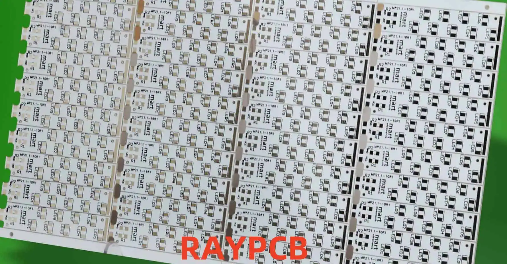
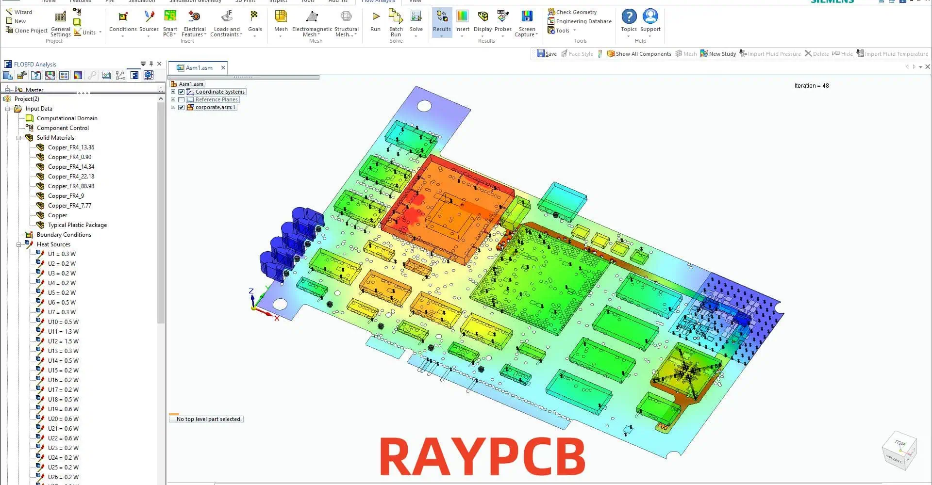
Aluminum PCBs (Metal Core PCBs or MCPCBs) have become increasingly important in high-power electronic applications due to their superior thermal management capabilities. This article explores the fundamentals of heat dissipation in aluminum PCBs and presents comprehensive design methodologies for optimal thermal performance.

Fundamentals of Aluminum PCB Construction

Material Layer Structure

LayerMaterialTypical ThicknessThermal Conductivity
Top LayerCopper35-70μm398 W/m·K
DielectricThermally Conductive75-150μm1-7 W/m·K
Base LayerAluminum0.8-3.0mm237 W/m·K
Surface FinishHASL/ENIG3-15μmVaries

Thermal Properties Comparison

Material TypeThermal Conductivity (W/m·K)Cost FactorWeight Factor
FR-40.2-0.311
Aluminum PCB1.0-7.02.0-3.01.5-2.0
Ceramic PCB20-2704.0-8.02.0-3.0
Copper Core3985.0-10.02.5-3.5

Heat Dissipation Mechanisms

heat dissipation in electronic devices

Primary Heat Transfer Methods

MethodContributionEfficiency Factor
Conduction60-70%High
Convection20-30%Medium
Radiation5-10%Low

Thermal Resistance Path

Path ComponentTypical Range (°C/W)Optimization Method
Junction to Case0.5-3.0Die attach material
Case to Board1.0-5.0Thermal interface
Board to Ambient5.0-20.0Cooling solution

Design Methodologies

Component Layout Guidelines

Thermal Spacing Requirements

Component PowerMinimum SpacingRecommended Spacing
<1W2mm5mm
1-3W5mm10mm
3-5W10mm15mm
>5W15mm20mm

Copper Design Rules

FeatureSpecificationPurpose
Minimum Width0.2mmCurrent capacity
Thermal Relief0.3mmAssembly control
Thermal Via Diameter0.3-0.5mmHeat transfer
Via Spacing1.0-1.5mmThermal distribution

Thermal Design Considerations

Thermal Via Implementation

ParameterValueNotes
Via Diameter0.3-0.5mmPlated through-hole
Via Spacing1.0-1.5mmGrid pattern
Plating Thickness25μmMinimum
Fill TypeSolid/PasteApplication dependent

Thermal Pattern Design

Pattern TypeThermal EfficiencyCost Impact
Solid Plane100%Baseline
Grid Pattern80-90%-10%
Star Pattern70-80%-20%
Custom Pattern60-95%Varies

Performance Optimization

Thermal Management Solutions

Solution TypeHeat DissipationCost ImpactIntegration Complexity
Heat SinkUp to 70%MediumMedium
Forced AirUp to 85%HighHigh
Thermal PasteUp to 30%LowLow
Liquid CoolingUp to 95%Very HighVery High

Material Selection Guidelines

ComponentRecommended MaterialThermal ConductivityCost Factor
Base MaterialAL5052138 W/m·K1
DielectricHigh Tg Epoxy1.0-7.0 W/m·K1.5-3.0
Thermal InterfaceSilicone Based3.0-5.0 W/m·K2.0-4.0
Surface FinishENIGN/A1.5-2.0

Manufacturing Considerations

Process Parameters

Process StepTemperature RangeTime DurationCritical Parameters
Preheating150-170°C60-90sRamp rate
Soldering230-250°C30-60sPeak temperature
Cooling4°C/s maxN/ACooling rate

Quality Control Methods

Test TypeMethodAcceptance Criteria
Thermal ResistanceASTM D5470≤0.4°C/W
Dielectric StrengthASTM D149≥3kV
Thermal Cycling-40 to +125°C1000 cycles
Thermal Shock-65 to +150°C300 cycles

Performance Evaluation

Thermal Testing Methods

Test MethodParameters MeasuredEquipment Required
IR ScanningSurface temperatureThermal camera
ThermocouplePoint temperatureData logger
Thermal ResistanceOverall performanceThermal tester
CFD AnalysisAirflow patternsSoftware

Performance Metrics

MetricTarget RangeCritical Factor
Junction Temperature≤125°CComponent reliability
Thermal Resistance≤0.4°C/WHeat dissipation
Temperature Rise≤40°CSystem performance
Temperature Uniformity±5°CThermal stress

Frequently Asked Questions

Q1: What are the key advantages of using aluminum PCBs over traditional FR-4 boards?

A1: Aluminum PCBs offer several significant advantages:

  • Superior thermal conductivity (1.0-7.0 W/m·K vs 0.2-0.3 W/m·K for FR-4)
  • Better dimensional stability at high temperatures
  • Enhanced reliability for high-power applications
  • Reduced need for additional cooling solutions
  • Longer lifespan of components due to better heat management

Q2: How can thermal via design be optimized for maximum heat dissipation?

A2: Optimal thermal via design involves several key considerations:

  • Via diameter should be 0.3-0.5mm for best performance
  • Grid pattern spacing of 1.0-1.5mm is recommended
  • Copper plating thickness should be minimum 25μm
  • Consider filled vias for better thermal conductivity
  • Implement proper via pattern beneath high-power components

Q3: What are the critical factors in selecting dielectric materials for aluminum PCBs?

A3: Critical factors include:

  • Thermal conductivity (higher is better)
  • Dielectric strength (minimum 3kV)
  • Glass transition temperature (Tg)
  • Thermal expansion coefficient
  • Cost considerations
  • Manufacturing compatibility

Q4: How does component placement affect thermal performance?

A4: Component placement significantly impacts thermal performance through:

  • Spacing between high-power components
  • Proximity to board edges
  • Air flow considerations
  • Thermal interaction between components
  • Access for additional cooling solutions

Q5: What are the common failure modes in aluminum PCBs and how can they be prevented?

A5: Common failure modes and prevention methods include:

  • Delamination (use proper material selection and processing)
  • Thermal stress (implement proper thermal relief design)
  • Solder joint failure (use appropriate thermal profiles)
  • Warpage (consider CTE matching in design)
  • Dielectric breakdown (select appropriate dielectric material)

Conclusion

Aluminum PCB design for optimal heat dissipation requires careful consideration of material selection, layout design, and manufacturing processes. Success depends on understanding thermal management principles and implementing appropriate design methodologies. Regular testing and validation ensure that thermal performance meets design requirements. As power densities continue to increase, the importance of effective thermal management in aluminum PCBs will only grow.

BGA Solderability Standard: Comprehensive Guidelines and Requirements

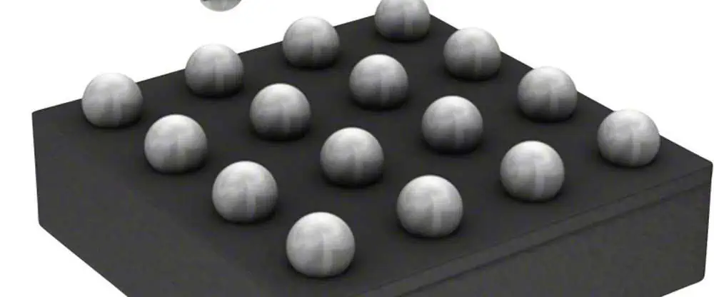
Ball Grid Array (BGA) solderability is crucial for ensuring reliable electronic assemblies. This comprehensive guide covers industry standards, testing methods, acceptance criteria, and best practices for BGA soldering processes. Understanding and implementing these standards is essential for achieving high-quality, reliable electronic assemblies.

Industry Standards Overview

Applicable Standards

StandardDescriptionScope
IPC-A-610Acceptability of Electronic AssembliesGeneral assembly requirements
J-STD-001Requirements for Soldered Electrical AssembliesSoldering requirements
IPC/JEDEC J-STD-020Moisture Sensitivity ClassificationPackage handling
IPC-7095Design and Assembly Process Implementation for BGAsBGA-specific guidelines

BGA Solder Ball Specifications

Physical Requirements

Ball Dimension Standards

Ball DiameterPitchTolerancePackage Size
0.30mm0.50mm±0.02mm≤15mm × 15mm
0.35mm0.65mm±0.02mm≤17mm × 17mm
0.45mm0.80mm±0.025mm≤23mm × 23mm
0.60mm1.00mm±0.03mm≤27mm × 27mm

Material Composition

TypeCompositionMelting PointApplication
SAC305Sn96.5/Ag3.0/Cu0.5217-220°CLead-free standard
SAC405Sn95.5/Ag4.0/Cu0.5217-220°CHigher reliability
SnPbSn63/Pb37183°CLegacy systems
SAC105Sn98.5/Ag1.0/Cu0.5217-220°CCost-effective

Solderability Requirements

Surface Finish Compatibility

Surface FinishCompatibility RatingShelf LifeComments
ENIGExcellent12 monthsPreferred choice
HASLGood6 monthsTraditional option
OSPGood3-6 monthsCost-effective
Immersion TinVery Good6 monthsGood wettability
ENEPIGExcellent12 monthsHigh reliability

Wettability Requirements

ParameterSpecificationTest Method
Wetting Time≤1.5 secondsIPC-J-STD-003
Wetting Force≥0.3N/mmIPC-TM-650
Contact Angle≤45 degreesVisual inspection
Coverage≥95%X-ray inspection

Process Parameters

Reflow Profile Requirements

Profile ZoneTemperatureTimeRate
Preheat150-180°C60-120s1-3°C/s
Soak180-200°C60-120sN/A
Reflow230-250°C30-90sN/A
Peak245-260°C10-30sN/A
CoolingBelow 180°CN/A-4°C/s max

Environmental Conditions

ParameterRequirementTolerance
Humidity30-60% RH±5%
Temperature20-26°C±2°C
Oxygen Level<1000ppm±100ppm
Air Flow0.5-2.0 m/s±0.2 m/s

Quality Assessment

Inspection Criteria

X-ray Inspection Standards

Defect TypeAcceptance CriteriaInspection Method
Voids<25% total areaX-ray
BridgingNone allowedX-ray/Visual
Misalignment<25% of ball diameterX-ray
Ball Shape75-125% nominal heightX-ray

Reliability Testing Requirements

Test TypeConditionsDurationAcceptance Criteria
Temperature Cycling-40°C to +125°C1000 cyclesNo failures
Drop Test1500G, 0.5ms30 dropsNo electrical discontinuity
Vibration10-100Hz30 minutesNo failures
HAST130°C/85%RH96 hoursNo electrical failures

Defect Classification

x ray inspection
x ray inspection

Common Defects Categories

CategoryDescriptionAcceptance Level
Class 1Process IndicatorAcceptable
Class 2Minor DefectLimited acceptance
Class 3Major DefectNot acceptable
Class 4Critical DefectNot acceptable

Specific Defect Criteria

Defect TypeClass 2 LimitClass 3 Limit
Void Size<25%<15%
Misalignment<25%<15%
Solder BallNoneNone
Head-on-PillowNoneNone

Process Control Methods

Statistical Process Control Parameters

ParameterControl LimitAction Limit
Peak Temperature±5°C±8°C
Reflow Time±5s±10s
Cooling Rate±0.5°C/s±1°C/s
Void Content±5%±8%

Documentation Requirements

Document TypeUpdate FrequencyRetention Period
Process ParametersPer lot2 years
Inspection ResultsPer board3 years
Calibration RecordsMonthly2 years
Training RecordsSemi-annual3 years

Troubleshooting Guide

Common Issues and Solutions

IssuePossible CausesCorrective Actions
Excessive VoidingInsufficient preheatAdjust profile
Poor WettingContaminated surfaceClean/replace finish
BridgingExcessive pasteAdjust stencil design
Head-on-PillowPoor thermal profileOptimize profile

Frequently Asked Questions

Q1: What are the critical factors affecting BGA solderability?

A1: The critical factors include:

  • Surface finish quality and compatibility
  • Reflow profile parameters
  • Component storage and handling
  • PCB pad design and finish
  • Solder paste composition and volume
  • Environmental conditions during assembly

Q2: How can void content in BGA solder joints be minimized?

A2: Void content can be minimized through:

  • Optimized reflow profile with adequate soak time
  • Proper solder paste selection and storage
  • Appropriate stencil design and aperture size
  • Controlled atmosphere reflow (nitrogen)
  • Proper pad design and surface finish
  • Regular maintenance of reflow equipment

Q3: What are the acceptable criteria for BGA solder joint inspection?

A3: Acceptable criteria include:

  • Void content less than 25% of total joint area
  • Complete wetting around ball circumference
  • No bridging between adjacent balls
  • Proper ball collapse height
  • No evidence of head-on-pillow defects
  • Proper alignment within 25% of ball diameter

Q4: How does surface finish selection impact BGA solderability?

A4: Surface finish selection impacts:

  • Initial wettability
  • Shelf life of PCB
  • Intermetallic compound formation
  • Long-term reliability
  • Process window flexibility
  • Overall assembly cost

Q5: What are the key considerations for BGA reflow profiling?

A5: Key considerations include:

  • Package size and thermal mass
  • Maximum temperature ratings
  • Solder paste requirements
  • PCB thickness and complexity
  • Component mix on the board
  • Required throughput speed

Conclusion

Maintaining high standards for BGA solderability is essential for producing reliable electronic assemblies. Following these guidelines and standards helps ensure consistent quality and reliability in BGA assembly processes. Regular monitoring, documentation, and process control are key to maintaining these standards. As technology continues to evolve, staying current with the latest standards and best practices remains crucial for successful BGA assembly operations.

A Comparison of Multiple PCB Design and EDA Simulation Tools

In today’s electronic design landscape, choosing the right PCB design and EDA simulation tool is crucial for successful project completion. This comprehensive comparison examines popular tools, their capabilities, strengths, and limitations to help engineers and designers make informed decisions for their specific needs.

Major PCB Design Tools Overview

Industry Leaders Comparison

FeatureAltium DesignerKiCadEagleOrCADMentor PADS
License TypeCommercialOpen SourceCommercialCommercialCommercial
Price Range$$$$Free$$$$$$$$$$
Learning CurveSteepModerateModerateSteepSteep
Cloud CapabilityYesLimitedYesYesYes
Library SizeExtensiveGoodGoodExtensiveExtensive
Multi-user SupportYesLimitedLimitedYesYes

Core Capabilities Matrix

Schematic Design Features

FeatureAltium DesignerKiCadEagleOrCADMentor PADS
Hierarchical Design✓✓✓✓✓✓✓✓✓✓✓✓✓
Custom Component Creation✓✓✓✓✓✓✓✓✓✓✓✓✓
Symbol EditorAdvancedBasicIntermediateAdvancedAdvanced
Multi-channel Design✓✓✓✓✓✓✓✓✓✓✓

Detailed Analysis of EDA Simulation Tools

Signal Integrity Tools

Comparison of SI Analysis Capabilities

CapabilityHyperLynxHSPICEADSAllegro
Time DomainAdvancedAdvancedAdvancedAdvanced
Frequency DomainAdvancedBasicAdvancedIntermediate
Eye Diagram✓✓✓✓✓✓✓✓✓✓
Crosstalk Analysis✓✓✓✓✓✓✓✓✓✓

Power Integrity Analysis

FeatureAnsys SIwaveKeysight ADSCadence Sigrity
DC Analysis✓✓✓✓✓✓✓✓
AC Analysis✓✓✓✓✓✓✓✓✓
Thermal Analysis✓✓✓✓✓✓✓
EMI Analysis✓✓✓✓✓✓✓

Tool-Specific Features

Altium Designer

Key Strengths

  • Unified design environment
  • Advanced 3D PCB visualization
  • Robust component management
  • Native MCAD integration

Performance Metrics

FeaturePerformance RatingNotes
UI Response4.5/5Smooth operation with large designs
File Handling4.-5Good version control integration
Memory Usage3.5/5Can be resource-intensive
Multi-board Support5.-5Excellent multi-board capabilities

KiCad

Key Strengths

  • Open-source platform
  • Active community support
  • Python scripting support
  • Regular updates

Resource Requirements

ResourceMinimumRecommended
RAM4GB8GB+
ProcessorDual CoreQuad Core
Storage2GB10GB+
GPUBasicOpenGL Compatible

Specialized Features Comparison

High-Speed Design Capabilities

FeatureTool SupportImplementation Level
Differential Pair RoutingMost ToolsAdvanced
Length MatchingAll ToolsVaried
Impedance ControlMost ToolsAdvanced
Via StitchingAll ToolsBasic to Advanced

Manufacturing Output Capabilities

Output TypeTool SupportFormat Options
Gerber FilesAll ToolsRS-274X
Drill FilesAll ToolsExcellon
BOM ExportAll ToolsCSV, XML, Excel
Pick and PlaceMost ToolsCSV, TXT

Cost Analysis

License Models and Pricing

ToolLicense TypeAnnual CostPerpetual License
Altium DesignerSubscription$5,000-$10,000Available
KiCadOpen SourceFreeN/A
EagleSubscription$500-$1,000Not Available
OrCADSubscription$4,000-$8,000Available
PADSSubscription$5,000-$9,000Available

Training and Support Costs

Service TypeTypical Cost RangeDuration
Basic Training$500-$2,0002-5 days
Advanced Training$2,000-$5,0005-10 days
Technical SupportIncluded-$5,000/yearAnnual
Custom Training$3,000-$10,000Variable

Performance Benchmarks

Design Complexity Handling

ToolSmall ProjectsMedium ProjectsLarge Projects
AltiumExcellentExcellentGood
KiCadExcellentGoodFair
EagleExcellentGoodLimited
OrCADExcellentExcellentExcellent
PADSExcellentExcellentGood

Processing Speed Comparison

OperationAltiumKiCadEagleOrCAD
Board LoadingFastMediumFastFast
DRC CheckFastMediumMediumFast
RoutingVery FastFastMediumVery Fast
3D RenderingFastMediumSlowFast

Integration Capabilities

Third-party Tool Integration

Integration TypeSupport LevelCommon Tools
MCADAdvancedSolidWorks, Inventor
PLMModerateTeamCenter, Windchill
Version ControlGoodGit, SVN
ERPVariableSAP, Oracle

Frequently Asked Questions

Q1: Which PCB design tool is best for beginners?

A1: KiCad is often recommended for beginners due to its free availability, extensive documentation, active community support, and relatively gentle learning curve. It offers all essential features needed to complete basic to intermediate PCB designs while providing a pathway to more advanced capabilities as skills develop.

Q2: How do commercial tools justify their high costs compared to open-source alternatives?

A2: Commercial tools justify their costs through advanced features like integrated simulation capabilities, professional technical support, automated design rule checking, advanced routing algorithms, and enterprise-level integration capabilities. They often provide time-saving features that can significantly reduce design cycle time in professional environments.

Q3: What factors should be considered when choosing between different EDA tools?

A3: Key factors include:

  • Project complexity and requirements
  • Budget constraints
  • Team size and collaboration needs
  • Required integration with other tools
  • Available computing resources
  • Learning curve and training requirements
  • Long-term maintenance and support needs

Q4: How do different tools handle high-speed design requirements?

A4: Professional tools like Altium, OrCAD, and PADS provide advanced high-speed design features including controlled impedance routing, length matching, differential pair routing, and integrated signal integrity analysis. Open-source tools may require external tools or plugins for advanced high-speed design capabilities.

Q5: What are the key differences in simulation capabilities between various tools?

A5: Professional tools typically offer integrated simulation capabilities for signal integrity, power integrity, and EMI analysis. Tools like HyperLynx and ADS provide more advanced simulation capabilities but require separate licenses. Open-source tools often rely on external simulation tools or limited built-in capabilities.

Conclusion

The choice of PCB design and EDA simulation tools depends heavily on specific project requirements, budget constraints, and team capabilities. While commercial tools offer comprehensive features and professional support, open-source alternatives provide capable solutions for many applications. Understanding the strengths and limitations of each tool is crucial for making an informed decision that aligns with project needs and organizational capabilities.

The trend towards cloud-based tools and integrated design environments continues to shape the landscape of PCB design tools, with increasing emphasis on collaboration features and integration capabilities. Regular evaluation of available tools and their evolving capabilities remains important for maintaining competitive advantage in electronic design.

0201/Micro BGA PCB Tolerance: A Comprehensive Design Guide

The increasing demand for miniaturization in electronic devices has led to the widespread adoption of 0201 components and micro Ball Grid Array (BGA) packages. Understanding and managing PCB tolerances for these ultra-small components is crucial for successful assembly and reliable product performance. This comprehensive guide explores the critical aspects of PCB design, manufacturing tolerances, and best practices for working with 0201 components and micro BGAs.

Understanding 0201 Components

Dimensional Specifications

0201 components represent one of the smallest surface mount device (SMD) form factors available in mass production. The designation “0201” refers to the imperial measurements:

DimensionImperial (inches)Metric (mm)
Length0.024 ± 0.0020.60 ± 0.05
Width0.012 ± 0.0010.30 ± 0.03
Height0.006 ± 0.0010.15 ± 0.03
Terminal0.008 ± 0.0010.20 ± 0.03

Critical Tolerance Considerations

Pad Design Parameters

DSBGA
DSBGA

The pad design for 0201 components requires precise control of several key parameters:

ParameterMinimum (mm)Nominal (mm)Maximum (mm)
Pad Length0.250.30.35
Pad Width0.250.30.35
Pad Spacing0.20.250.3
Solder Mask0.050.080.1

Micro BGA Technology

Package Characteristics

Micro BGAs represent the cutting edge of surface mount technology, offering high I/O density in a compact footprint. Typical specifications include:

FeatureSpecification Range
Ball Pitch0.35mm – 0.80mm
Ball Diameter0.20mm – 0.45mm
Package Size2mm x 2mm to 14mm x 14mm
Ball Count36 to 400+

Critical Design Parameters

PCB Design Requirements

ParameterRequirement
Minimum Trace Width0.075mm
Minimum Spacing0.075mm
Via Diameter0.15mm – 0.20mm
Copper Thickness0.5oz – 1oz
Surface FinishENIG or ENEPIG

Manufacturing Tolerances

PCB Fabrication Tolerances

Layer Registration

Layer TypeTolerance (mm)
Inner Layer±0.050
Outer Layer±0.075
Via Registration±0.100
Solder Mask±0.075

Material Properties

PropertySpecification
Base MaterialHigh-Tg FR-4
Tg Minimum170°C
CTE (x-y)12-15 ppm/°C
CTE (z)50-70 ppm/°C

Assembly Tolerances

Component Placement

ParameterTolerance
X-Y Position±0.05mm
Rotation±1.0°
Coplanarity0.08mm max

Solder Paste Parameters

ParameterSpecification
Volume Tolerance±10%
Height Tolerance±0.025mm
Area Coverage80-90%

Design Guidelines

PCB Layout Recommendations

  1. Pad Design
    • Use solder mask defined (SMD) pads for micro BGAs
    • Implement tear-drop reinforcement on critical connections
    • Maintain consistent pad sizes within component groups
  2. Routing Considerations
    • Utilize micro vias for dense routing requirements
    • Implement fan-out strategies based on signal types
    • Maintain symmetrical routing for differential pairs

DFM Requirements

Manufacturing Specifications

RequirementValue
Min. Track Width0.075mm
Min. Space Width0.075mm
Aspect Ratio0.8:1
Min. Annular Ring0.125mm
Edge Clearance0.25mm

Quality Control Measures

Inspection Requirements

Automated Optical Inspection (AOI)

Inspection PointTolerance
Component Offset±0.10mm
Solder Joint Size±15%
Bridging Detection0.05mm
Missing Component100% detection

Testing Protocols

  1. In-Circuit Testing (ICT)
    • Test point accessibility
    • Probe force considerations
    • Coverage requirements
  2. X-ray Inspection
    • Void percentage limits
    • BGA ball alignment
    • Hidden solder joint quality

Best Practices for Assembly

Process Controls

Reflow Profile Parameters

PhaseTemperature (°C)Time (seconds)
Preheat150-17060-90
Soak170-19060-120
Reflow230-25030-60
Cooling<4°C/secN/A

Moisture Sensitivity Handling

MSL LevelFloor LifeConditions
1Unlimited≤30°C/85% RH
2a4 weeks≤30°C/60% RH
3168 hours≤30°C/60% RH

Troubleshooting Guide

Common Issues and Solutions

IssuePotential CauseSolution
Solder BridgingExcessive pasteAdjust stencil design
Component SkewingPoor placementImprove placement accuracy
Open JointsInsufficient pasteReview paste parameters
VoidsProfile issuesOptimize reflow profile

Frequently Asked Questions

xilinx-spartan-6-fpga-tutorial

Q1: What is the minimum recommended trace width for routing under micro BGAs?

A1: The minimum recommended trace width for routing under micro BGAs is 0.075mm (3 mils). However, it’s important to consider manufacturing capabilities and impedance requirements when selecting final trace dimensions.

Q2: How does moisture sensitivity affect micro BGA assembly?

A2: Moisture sensitivity can lead to package cracking during reflow if proper handling procedures aren’t followed. Components should be stored in moisture barrier bags with desiccant and humidity indicators, and floor life limitations must be strictly observed based on the MSL level.

Q3: What are the key considerations for selecting PCB surface finish for 0201 and micro BGA applications?

A3: ENIG or ENEPIG are preferred surface finishes due to their excellent planarity, solderability, and shelf life. These finishes provide consistent solderability and help prevent oxidation issues during assembly.

Q4: How can void percentage in micro BGA solder joints be minimized?

A4: Void percentage can be minimized through proper reflow profile optimization, using quality solder paste, implementing appropriate pad designs, and ensuring proper storage and handling of components and materials.

Q5: What are the recommended inspection methods for 0201 components and micro BGAs?

A5: A combination of AOI, X-ray inspection, and SPI (Solder Paste Inspection) is recommended. AOI can verify component placement and presence, X-ray inspection can check solder joint quality and void content, while SPI ensures proper solder paste deposit volume and position.

Conclusion

Successfully implementing 0201 components and micro BGAs requires careful attention to PCB design tolerances, manufacturing processes, and quality control measures. By following the guidelines and specifications outlined in this document, engineers can achieve reliable and consistent assembly results. Regular review and updates of these parameters based on production feedback and new technology developments will help maintain high-quality standards in electronic assembly.

Several PCBA Test and Inspection Methods

Printed Circuit Board Assembly (PCBA) testing and inspection are crucial steps in ensuring the quality and reliability of electronic products. This comprehensive guide explores various testing and inspection methods, their applications, advantages, and limitations in modern electronics manufacturing.

Visual Inspection Methods

Manual Visual Inspection

AspectSpecificationStandard Reference
Magnification3x-10xIPC-A-610
Lighting800-1000 luxIPC-A-610
Inspector QualificationIPC CertifiedJ-STD-001
Inspection Time2-5 min/boardIndustry Average

Automated Optical Inspection (AOI)

FeatureCapabilityDetection Accuracy
Component Presence±0.1mm99.90%
Polarity CheckComponent specific99.80%
Solder Joint Analysis01005 to QFP99.50%
Foreign Material>0.1mm98%

AOI System Specifications

ParameterEntry LevelMid-RangeHigh-End
Resolution15μm10μm5μm
Speed15 cm²/s20 cm²/s30 cm²/s
False Call Rate<3%<2%<1%
Camera Type2D2D+3DMulti-angle 3D

Automated Testing Systems

RayMing AOI
RayMing AOI

In-Circuit Testing (ICT)

Test TypeParametersAccuracyTest Time
Continuity0.1Ω-100Ω±1%<50ms
Resistance1Ω-10MΩ±0.1%<100ms
Capacitance10pF-100μF±2%<150ms
Inductance1μH-100mH±3%<200ms

ICT Fixture Specifications

FeatureSpecificationImpact on Testing
Pin DensityUp to 100/in²Test coverage
Contact Force4-8 ozConnection reliability
Fixture Life>50,000 cyclesMaintenance interval
Setup Time2-4 hoursProduction efficiency

Flying Probe Testing

CapabilitySpecificationAdvantage
Point Access>0.2mmNo fixture needed
Test Speed20-30 points/sFlexible testing
Probe Types2-8 probesComplex measurements
ProgrammingAuto-generateQuick setup

Functional Testing

Basic Functional Test Parameters

Test CategoryParametersTest DurationPass Criteria
Power SupplyVoltage, Current30s±5% tolerance
Digital I/OLogic levels45sMatch truth table
Analog SignalsAmplitude, Frequency60s±2% tolerance
CommunicationProtocol integrity90sZero errors

Advanced Functional Testing

Test TypeCoverageEquipmentTime
Boundary ScanDigital circuitsJTAG tester2-5 min
Memory TestRAM/ROMMemory tester3-8 min
RF TestingWireless circuitsNetwork analyzer5-10 min
Power AnalysisPower circuitsPower analyzer4-7 min

Environmental Testing

Temperature Testing

Test TypeRangeDurationStandards
Operating-40°C to +85°C24-48hIPC-TM-650
Storage-55°C to +125°C168hMIL-STD-883
Thermal Cycle-40°C to +125°C100-1000 cyclesJESD22-A104
Thermal Shock-65°C to +150°C10-50 cyclesMIL-STD-202

Environmental Stress Testing

Test TypeConditionsDurationPurpose
Humidity85°C/85%RH168hMoisture resistance
Vibration10-2000Hz4h/axisMechanical stability
Salt Spray5% NaCl48-96hCorrosion resistance
Drop Test1-1.5m height6 dropsImpact resistance

X-ray and Thermal Analysis

SMT X RAY CHECKING

X-ray Inspection

FeatureCapabilityApplication
ResolutionDown to 0.5μmBGA/QFN inspection
MagnificationUp to 10000xVoid measurement
Viewing Angle0-70°Joint analysis
Detection2D/3D/CTInternal structure

Thermal Analysis

MethodTemperature RangeResolutionUse Case
IR Camera-20°C to +350°C0.05°CHot spot detection
Thermal Couples-200°C to +400°C0.1°CPoint measurement
Thermal Imaging-40°C to +500°C0.03°CHeat distribution
Heat Profiling0°C to +300°C1°CReflow analysis

Quality Standards and Compliance

Industry Standards

StandardScopeRequirementsUpdate Frequency
IPC-A-610AcceptabilityVisual criteria3-5 years
J-STD-001ProcessAssembly requirements2-4 years
ISO 9001Quality systemDocumentation3 years
IPC-6012PerformanceQualification4-5 years

Quality Metrics

MetricTargetMeasurement MethodFrequency
FPY>95%Production dataDaily
DPMO<50Defect trackingWeekly
Customer Returns<0.1%RMA analysisMonthly
Test Coverage>98%Test program analysisPer product

Frequently Asked Questions

Q1: Which testing method should be used for high-volume production?

A1: For high-volume production, a combination of AOI and ICT is recommended:

  • AOI provides rapid visual defect detection
  • ICT ensures comprehensive electrical testing
  • Combined coverage typically exceeds 98%
  • Cost-effective for volumes >10,000 units/month

Q2: How often should test equipment be calibrated?

A2: Test equipment calibration frequencies vary by type:

  • ICT systems: Every 6 months
  • AOI systems: Monthly calibration checks
  • Functional test equipment: Quarterly
  • Environmental chambers: Annually All calibrations must be traceable to national standards.

Q3: What is the typical test coverage achievable with different methods?

A3: Test coverage varies by method:

  • ICT: 90-95% of electrical defects
  • AOI: 90-98% of visual defects
  • Flying Probe: 85-90% of electrical defects
  • Functional Test: 70-80% of operational defects Combined methods can achieve >99% coverage.

Q4: How are testing requirements determined for new products?

A4: Testing requirements are determined through:

  1. Design complexity analysis
  2. Production volume consideration
  3. End-use environment evaluation
  4. Customer specifications review
  5. Industry standard requirements
  6. Cost-benefit analysis

Q5: What are the key factors affecting test quality and reliability?

A5: Key factors include:

  • Equipment calibration status
  • Operator training and certification
  • Environmental conditions
  • Test fixture maintenance
  • Program optimization
  • Regular system verification

Conclusion

PCBA testing and inspection methods continue to evolve with advancing technology and increasing quality requirements. A comprehensive testing strategy typically involves multiple complementary methods to achieve optimal quality assurance. Understanding the capabilities, limitations, and appropriate applications of each testing method enables manufacturers to implement effective quality control processes while maintaining cost-effectiveness and production efficiency.

Online PCB Prototyping Quotes with Full Self-service

PCB prototype assembly suppliers

The evolution of PCB manufacturing has led to the development of sophisticated online quoting systems that provide engineers and designers with immediate pricing and ordering capabilities. This comprehensive guide explores the self-service PCB prototyping quote system, its features, and how to effectively utilize it for your project needs.

Self-service Quote System Overview

Core Features

Feature Description Benefit
Real-time Pricing Instant cost calculation based on specifications Immediate budget planning
DFM Check Automated design rule checking Reduces manufacturing errors
File Upload Support Multiple format compatibility Design flexibility
Specification Editor Interactive parameter adjustment Custom requirements
Price Optimization Automatic cost-saving suggestions Budget efficiency

Supported File Formats

Format Type Extension Version Support
Gerber .gbr, .gbl, .gtl RS-274X
CAD .brd, .sch Eagle, Altium
ODB++ .tgz, .zip 7.0+
Excellon .drl, .txt 1.1, 2.0

PCB Specifications and Options

Board Parameters

Base Materials

Material Type Tg Value Available Thickness Price Factor
FR4 130-140°C 0.4-3.2mm 1.0x
High Tg FR4 170-180°C 0.6-3.2mm 1.3x
Rogers 200°C+ 0.254-3.175mm 3.5x
Aluminum N/A 1.0-3.0mm 2.0x

Layer Count Options

Layer Count Turn Time Min Trace Width Min Space
1-2 24h 4mil 4mil
4-6 48h 4mil 4mil
8-10 72h 5mil 5mil
12+ 96h 5mil 5mil

Surface Finish Options

Finish Type Thickness Shelf Life Price Factor
HASL Lead-Free 1-40μin 12 months 1.0x
ENIG 3-6μin 12 months 1.5x
Immersion Silver 8-16μin 6 months 1.3x
OSP 0.2-0.5μm 3 months 0.9x

Pricing Structure

Base Price Factors

Factor Impact Calculation Method
Board Size Primary Area in sq. inches × base rate
Layer Count Primary Base × layer multiplier
Material Secondary Base × material factor
Quantity Variable Sliding scale discount

Quantity Discount Structure

Quantity Range Discount Level Lead Time Impact
1-5 Standard Price Standard
6-20 10% off +0 days
21-50 15% off +1 day
51-100 20% off +2 days
101-500 25% off +3 days

Special Features Pricing

Feature Additional Cost Time Impact
Controlled Impedance 15% +1 day
Blind/Buried Vias 30% +2 days
Rush Order 50% -50% time
Advanced DFM 10% +1 day

Order Process and Timeline

Standard Process Flow

Stage Duration Key Activities
Quote Generation Instant Specification input, file upload
DFM Review 2-4 hours Automated + manual check
Manufacturing 24-96 hours Based on specifications
Testing 4-8 hours Electrical + visual inspection
Shipping 1-5 days Based on method

Order Tracking Milestones

Milestone Notification Action Required
Order Placed Email + SMS Payment confirmation
DFM Complete Email Review and approve
Production Start Email None
Testing Complete Email None
Shipping Email + SMS None

Quality Assurance

Prototype PCB Assembly

Testing Procedures

Test Type Parameters Standard Coverage
Electrical Continuity, shorts IPC-9252 100%
Visual Surface defects IPC-A-600 100%
Impedance ±10% tolerance IPC-2141 Sample
Solderability Wetting J-STD-003 Sample

Quality Metrics

Metric Target Measurement Method
First Pass Yield >98% Production statistics
Customer Satisfaction >95% Survey results
On-time Delivery >97% Shipping records
DFM Accuracy >99% Issue tracking

Frequently Asked Questions

Q1: How accurate are the online quotes compared to final pricing?

A1: Online quotes are 100% accurate for standard specifications. Additional costs may only apply if specifications are changed after the quote or if DFM review identifies necessary modifications. Any potential changes are communicated before production begins.

Q2: What is the minimum order quantity for PCB prototypes?

A2: There is no minimum order quantity. You can order as little as one piece. However, due to setup costs, the per-unit price decreases significantly with larger quantities. See our quantity discount structure table for detailed pricing breaks.

Q3: How are design files protected during the online quoting process?

A3: All uploaded files are protected through:

  • 256-bit SSL encryption during transfer
  • Secure cloud storage with encryption at rest
  • Automated file deletion after 30 days
  • Non-disclosure agreement coverage
  • Access restricted to essential personnel only

Q4: What happens if the automated DFM check finds issues?

A4: If the automated DFM check identifies issues:

  1. You receive an immediate notification with detailed report
  2. Suggested modifications are provided
  3. You can either update your design or approve production with acknowledged risks
  4. Technical support is available for consultation

Q5: Can rush orders be accommodated through the self-service system?

A5: Yes, rush orders can be processed through the self-service system with:

  • 50% expedite fee for half standard lead time
  • Available for boards up to 8 layers
  • Automatic availability check based on current capacity
  • Priority handling at all stages

Conclusion

The self-service PCB prototyping quote system represents a significant advancement in PCB manufacturing accessibility and efficiency. Through automated processes, comprehensive specification options, and transparent pricing, it enables designers and engineers to quickly obtain accurate quotes and proceed with manufacturing. The system’s integration of DFM checks, quality assurance, and tracking capabilities ensures a smooth and reliable production process from quote to delivery.

Audited PCB Fabrication Equipment by RAYMING

RAYMING’s commitment to excellence in PCB fabrication is exemplified through its comprehensive suite of audited manufacturing equipment. This article provides an in-depth examination of the state-of-the-art machinery and systems employed in their production facilities, ensuring the highest quality printed circuit boards for various applications.

Core PCB Manufacturing Equipment

Drilling Systems

RAYMING’s drilling equipment represents the cornerstone of precise PCB fabrication. The following table outlines the key specifications of their drilling systems:

System TypeTemperature RangeMax PressureCycle TimeLayer Capacity
Vacuum Press20-400°C600 PSI45-180 minUp to 48 layers
Hot Oil Press20-350°C500 PSI30-150 minUp to 32 layers
Sequential Press20-380°C550 PSI40-160 minUp to 40 layers

Lamination Systems

The lamination process requires precise control of temperature, pressure, and timing. RAYMING’s lamination equipment includes:

FeatureSpecification
ResolutionDown to 25μm
Alignment Accuracy±7.5μm
ThroughputUp to 240 sides/hour
Field Size24″ x 30″ maximum

Exposure Systems

Direct Imaging Systems

Modern direct imaging systems ensure precise pattern transfer with the following specifications:

FeatureSpecification
ResolutionDown to 25μm
Alignment Accuracy±7.5μm
ThroughputUp to 240 sides/hour
Field Size24″ x 30″ maximum

UV Exposure Units

Traditional UV exposure units maintain their importance for specific applications:

TypeExposure AreaWavelengthPower
LED UV30″ x 36″365-405nm5000W
Mercury Arc24″ x 30″350-420nm6000W

Quality Control and Testing Equipment

Automated Optical Inspection (AOI)

RAYMING’s AOI systems provide comprehensive defect detection:

CapabilitySpecification
Resolution5μm pixel size
Scan Speed50 cm²/second
False Call Rate<1%
Defect Categories32 types

Electrical Testing Equipment

Flying Probe Testers

FeatureSpecification
Test PointsUp to 200,000
Accuracy±25μm
Test Speed160 points/second
Probe Types4-8 flying probes

Advanced PCB Processing Systems

Surface Treatment Equipment

Process TypeCapabilityTreatment TimeUniformity
ENIG2-3 μin gold45-60 min±10%
HASLLead-free20-30 sec±15%
OSP0.2-0.5μm2-3 min±8%

Etching Systems

System TypeEtch RateLine Width CapabilityChemistry
Spray Etcher35μm/minDown to 75μmAlkaline
Bubble Etcher30μm/minDown to 100μmAcid

Safety and Environmental Protection Equipment

Waste Treatment Systems

System TypeCapacityTreatment MethodEfficiency
Water Treatment50,000 L/dayMulti-stage filtration99.90%
Air Purification10,000 m鲁/hourActivated carbon99.50%
Chemical Recycling5,000 L/dayDistillation95%

Safety Monitoring Equipment

Equipment TypeParameters MonitoredAlert ThresholdResponse Time
Gas DetectorsVOCs, acid fumes10 ppm<3 seconds
Temperature SensorsProcess heat±2°C variationReal-time
Pressure MonitorsSystem pressure±5% variationImmediate

Industry Standards and Compliance

Certification Requirements

StandardScopeAudit FrequencyKey Requirements
ISO 9001:2015Quality ManagementAnnualProcess control
IPC-6012PCB PerformanceBi-annualReliability specs
UL 796Safety StandardsAnnualMaterial testing

Equipment Maintenance Protocols

Equipment TypeMaintenance IntervalCalibration FrequencyDocumentation
CNC MachinesWeeklyMonthlyDigital logs
Testing EquipmentDailyQuarterlyCalibration certificates
Process ControlsMonthlySemi-annualMaintenance records

Frequently Asked Questions

Q1: What is the maximum PCB layer count that RAYMING’s equipment can handle?

A1: RAYMING’s lamination systems can process PCBs with up to 48 layers using the vacuum press system. However, optimal production efficiency is achieved with 32-layer boards using the hot oil press system.

Q2: How often is the manufacturing equipment calibrated?

A2: Critical equipment undergoes regular calibration based on usage and type:

  • Testing equipment: Quarterly calibration
  • CNC machines: Monthly calibration
  • Process control equipment: Semi-annual calibration All calibrations are documented and traceable to national standards.

Q3: What are the minimum feature sizes achievable with RAYMING’s equipment?

A3: The current equipment capabilities allow for:

  • Minimum trace width: 75μm
  • Minimum hole size: 0.1mm
  • Registration accuracy: ±0.025mm

Q4: How does RAYMING ensure environmental compliance in their manufacturing process?

A4: Environmental compliance is maintained through:

  • Advanced water treatment systems processing 50,000 L/day
  • Air purification systems handling 10,000 m³/hour
  • Chemical recycling systems processing 5,000 L/day All systems are monitored real-time and maintain compliance with local and international environmental standards.

Q5: What quality control measures are in place for PCB production?

A5: Quality control is maintained through multiple systems:

  • Automated Optical Inspection with 5μm resolution
  • Flying probe testing with 160 points/second capability
  • Regular equipment calibration and maintenance
  • Comprehensive documentation and traceability systems

Conclusion

RAYMING’s audited PCB fabrication equipment represents a comprehensive and modern manufacturing capability. The combination of precise machinery, rigorous quality control systems, and commitment to environmental protection ensures the production of high-quality PCBs that meet or exceed industry standards. Regular audits and maintenance protocols maintain the equipment’s optimal performance, while advanced testing and inspection systems guarantee product quality. This investment in technology and quality control positions RAYMING as a reliable partner for complex PCB manufacturing requirements.

Working with SV Microwave Solderless Compression Connectors for RF PCBs

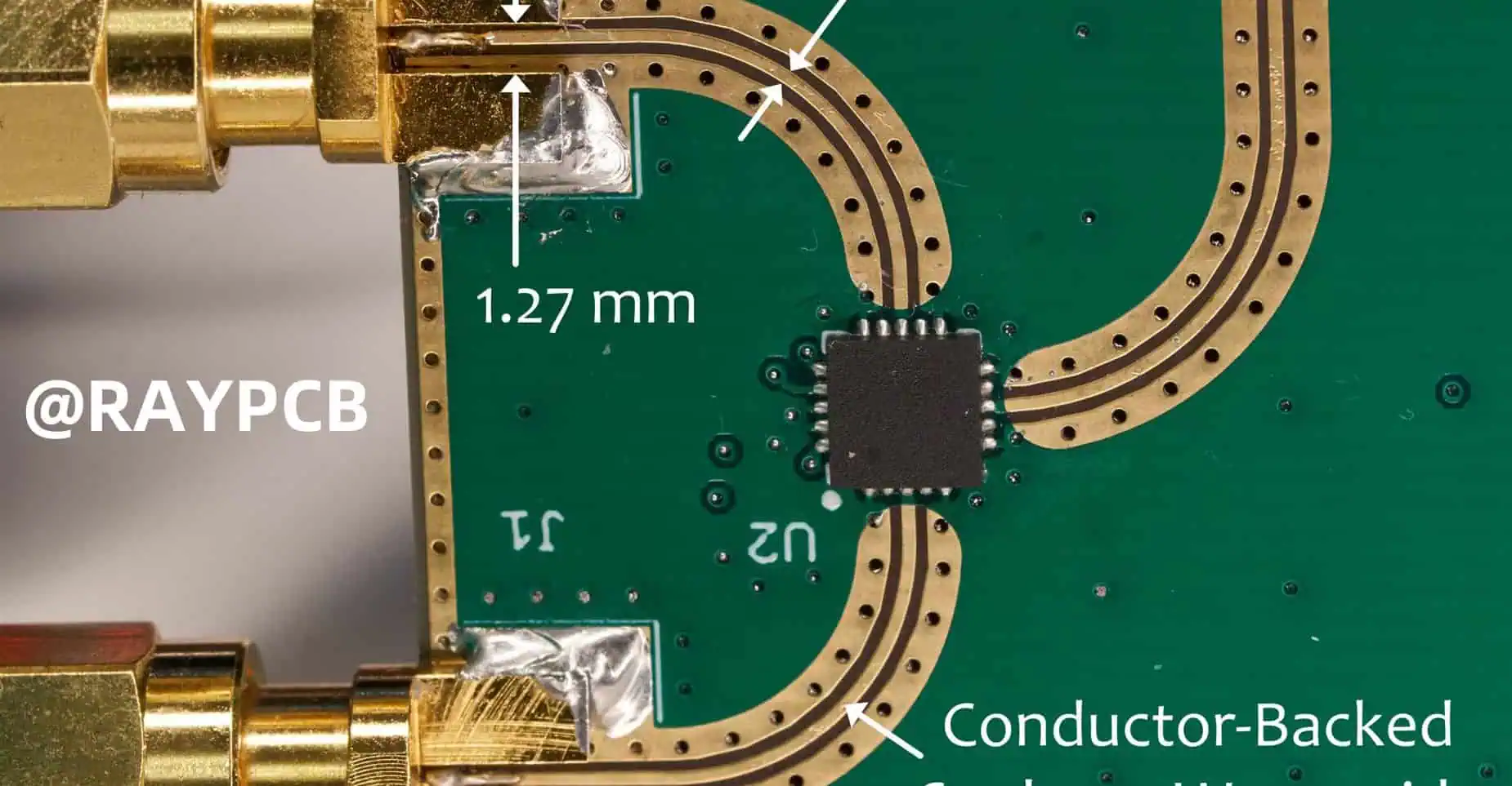
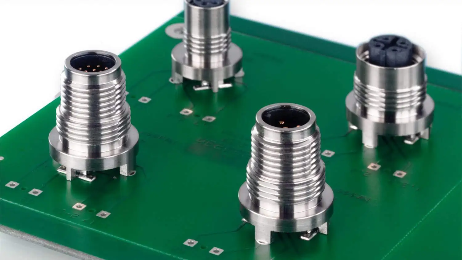
In the world of radio frequency (RF) electronics, the choice of connectors plays a crucial role in maintaining signal integrity and ensuring optimal performance. SV Microwave Solderless Compression Connectors have emerged as a game-changing solution for RF printed circuit boards (PCBs), offering numerous advantages over traditional soldered connections. This comprehensive guide will explore the intricacies of working with these innovative connectors, their benefits, installation techniques, and best practices for achieving superior RF performance.

Understanding SV Microwave Solderless Compression Connectors


What Are Solderless Compression Connectors?

Solderless compression connectors, as the name suggests, are RF connectors that do not require soldering for installation. Instead, they utilize mechanical pressure to establish a secure and reliable electrical connection between the connector and the PCB. SV Microwave, a leading manufacturer in the RF industry, has developed a line of high-performance solderless compression connectors designed specifically for RF applications.

Key Features and Benefits

SV Microwave Solderless Compression Connectors offer several advantages over traditional soldered connectors:

  1. Quick and Easy Installation: The solderless design allows for faster assembly and reduced production time.
  2. Improved Reliability: Eliminates the risk of cold solder joints and thermal stress on components.
  3. Consistent Performance: Mechanical compression ensures uniform contact pressure across all connections.
  4. Reworkability: Connectors can be easily removed and replaced without damaging the PCB.
  5. Enhanced RF Performance: Optimized design for superior electrical performance at high frequencies.
  6. Thermal Management: Reduced heat exposure during installation helps protect sensitive components.

Types of SV Microwave Solderless Compression Connectors

SV Microwave offers a variety of solderless compression connectors to suit different RF applications:

Connector Type Frequency Range Impedance Common Applications
SMA DC – 18 GHz 50 Ohm General RF, Test & Measurement
2.92mm DC – 40 GHz 50 Ohm High-frequency RF, Millimeter-wave
2.4mm DC – 50 GHz 50 Ohm Microwave, Satellite Communications
1.85mm DC – 65 GHz 50 Ohm Millimeter-wave, 5G
1.0mm DC – 110 GHz 50 Ohm Extremely high-frequency applications

Designing RF PCBs for Solderless Compression Connectors

PCB Layout Considerations

When designing RF PCBs for use with SV Microwave Solderless Compression Connectors, several factors must be taken into account:

  1. Footprint Design: Ensure that the PCB footprint matches the specific connector model’s requirements.
  2. Trace Impedance: Maintain consistent impedance throughout the signal path, including the transition to the connector.
  3. Ground Plane: Implement a solid ground plane beneath the signal traces to minimize signal loss and interference.
  4. Clearance: Provide adequate clearance around the connector for proper tool access during installation.

Material Selection

The choice of PCB material is critical for optimal RF performance:

Material Dielectric Constant (εr) Loss Tangent Suitable Frequency Range
FR-4 4.3 – 4.7 0.02 – 0.03 Up to 4 GHz
Rogers 4350B 3.48 0.0037 Up to 10 GHz
Rogers 5880 2.2 0.0009 Up to 77 GHz
PTFE 2.1 0.0002 Up to 110 GHz

Select a material that balances performance requirements with cost considerations for your specific application.

Installation Process for SV Microwave Solderless Compression Connectors

Preparation

Before installing the connectors, ensure you have the following:

  1. Clean work surface
  2. ESD-safe environment
  3. Appropriate compression tool
  4. Connector-specific installation fixtures (if required)
  5. Torque wrench (for securing the connector body)
  6. Cleaning supplies (isopropyl alcohol, lint-free cloth)

Step-by-Step Installation Guide

  1. Inspect the PCB: Ensure the PCB footprint matches the connector specifications and is free from defects.

  2. Clean the PCB: Use isopropyl alcohol and a lint-free cloth to remove any contaminants from the connection area.

  3. Align the Connector: Carefully position the connector on the PCB, ensuring proper alignment with the footprint.

  4. Apply Compression: Using the appropriate compression tool, apply even pressure to secure the connector to the PCB.

  5. Verify Connection: Inspect the connection visually and electrically to ensure proper contact and alignment.

  6. Secure the Connector Body: If applicable, use a torque wrench to tighten the connector body to the specified torque value.

  7. Final Inspection: Perform a final visual and electrical inspection to confirm the installation’s quality.

Common Installation Pitfalls and How to Avoid Them

  1. Misalignment: Use alignment fixtures or guides to ensure precise positioning of the connector.
  2. Over-compression: Follow manufacturer guidelines for compression force to avoid damaging the connector or PCB.
  3. Contamination: Maintain a clean work environment and handle components with care to prevent contamination.
  4. Improper Tools: Use only tools specifically designed for SV Microwave Solderless Compression Connectors.

Testing and Verification

Electrical Testing

After installation, perform the following electrical tests to verify proper connection and performance:

  1. Continuity Test: Ensure electrical continuity between the connector and PCB traces.
  2. Isolation Test: Verify that there are no short circuits between signal and ground.
  3. Insertion Loss Measurement: Measure the signal loss across the connector-PCB interface.
  4. Return Loss / VSWR Measurement: Evaluate the impedance matching quality of the connection.
  5. Time Domain Reflectometry (TDR): Analyze the connector-PCB transition for impedance discontinuities.

Mechanical Testing

Perform these mechanical tests to ensure the connector’s physical integrity:

  1. Pull Test: Apply a specified axial force to verify the connector’s mechanical strength.
  2. Torque Test: For threaded connectors, verify that they can withstand the specified mating torque.
  3. Vibration Test: Subject the assembly to vibration to ensure the connection remains stable.

Maintaining RF Performance

Best Practices for Optimal Performance

  1. Proper Grounding: Implement a comprehensive grounding strategy to minimize noise and interference.
  2. Signal Integrity: Use appropriate PCB design techniques to maintain signal quality, such as controlled impedance traces and minimizing vias.
  3. Shielding: Incorporate effective shielding measures to protect sensitive RF circuits from external interference.
  4. Thermal Management: Consider the thermal impact of high-frequency operation and implement appropriate cooling solutions.

Troubleshooting Common Issues

Issue Possible Causes Solutions
High Insertion Loss Poor contact, contamination Re-clean and re-compress the connection
Intermittent Connection Insufficient compression, PCB warpage Verify compression force, check PCB flatness
Frequency Response Deviation Impedance mismatch, improper grounding Review PCB layout, improve grounding
Mechanical Instability Over-torquing, improper fixture use Follow torque specifications, use correct tools

Advanced Applications and Future Trends

RF Filter
RF Filter

High-Speed Digital Applications

As data rates continue to increase, SV Microwave Solderless Compression Connectors are finding applications in high-speed digital systems:

  1. Data Centers: High-density, high-bandwidth interconnects
  2. 5G Infrastructure: Millimeter-wave frequency support for next-generation networks
  3. Automotive Radar: Precision connectors for advanced driver assistance systems (ADAS)

Emerging Technologies

SV Microwave continues to innovate in the field of solderless compression connectors:

  1. Higher Frequency Support: Development of connectors for sub-THz and THz applications
  2. Miniaturization: Smaller form factors for dense PCB layouts and portable devices
  3. Multi-port Connectors: Integrated solutions for complex RF systems
  4. Smart Connectors: Incorporation of built-in diagnostics and monitoring capabilities

Conclusion

SV Microwave Solderless Compression Connectors represent a significant advancement in RF PCB technology, offering improved performance, reliability, and ease of assembly. By understanding the design considerations, installation processes, and best practices outlined in this guide, engineers and technicians can leverage these innovative connectors to create high-performance RF systems for a wide range of applications.

As the demand for higher frequency and more compact RF solutions continues to grow, SV Microwave Solderless Compression Connectors are well-positioned to meet the challenges of next-generation wireless technologies and beyond.

Frequently Asked Questions (FAQ)

  1. Q: What is the maximum frequency range for SV Microwave Solderless Compression Connectors? A: SV Microwave offers solderless compression connectors that can support frequencies up to 110 GHz, such as their 1.0mm connector series.

  2. Q: Are special tools required for installing these connectors? A: Yes, SV Microwave provides specific compression tools and fixtures for proper installation of their solderless compression connectors. Using the correct tools is crucial for achieving optimal performance and reliability.

  3. Q: Can SV Microwave Solderless Compression Connectors be reused? A: While these connectors are designed for reworkability, repeated compression and decompression may affect their performance. It’s best to consult the manufacturer’s guidelines for specific reuse recommendations.

  4. Q: How do I ensure proper alignment when installing the connectors? A: Use alignment fixtures provided by SV Microwave, carefully follow the PCB footprint guidelines, and visually inspect the alignment before and after compression.

  5. Q: Are there any environmental considerations for using these connectors in extreme conditions? A: SV Microwave offers connectors designed for various environmental conditions. Consider factors such as temperature range, humidity, and vibration when selecting the appropriate connector series for your application. Always refer to the product specifications for detailed environmental ratings.

Mouse Bites PCB – Breakaway Tabs – V Groove PCB

Mouse Bites PCB

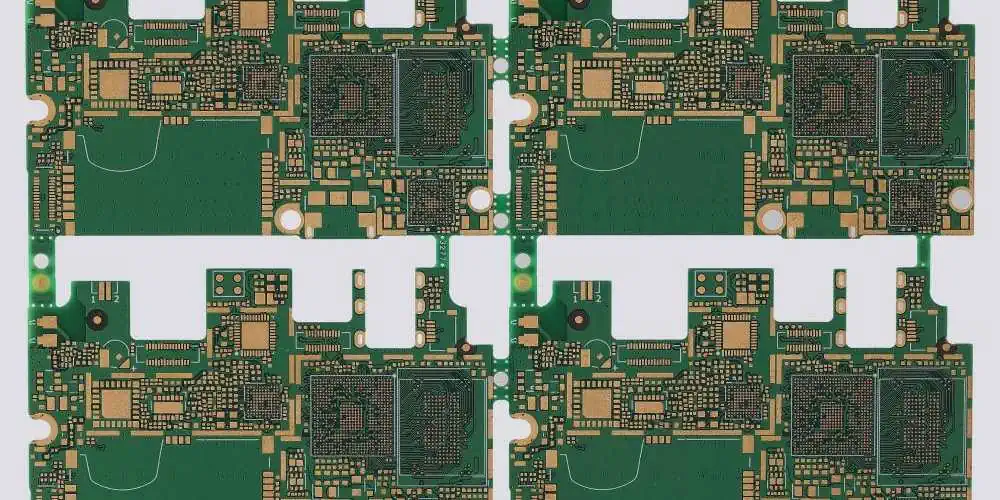
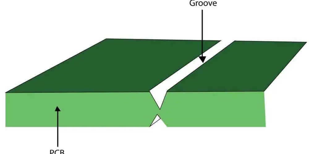
In PCB manufacturing, the need to separate individual boards from a larger panel efficiently and cleanly is crucial. Three primary methods have emerged as industry standards: Mouse Bites, Breakaway Tabs, and V-Grooves. Each method offers unique advantages and considerations for different production scenarios and requirements.

Mouse Bites in PCB Manufacturing

Definition and Characteristics

Mouse bites are small, perforated holes arranged in a line that allow for easy separation of PCBs from panels.

Technical Specifications

Parameter Typical Range Optimal Value Impact on Separation
Hole Diameter 0.5-1.0mm 0.7mm High
Hole Spacing 0.5-1.5mm 1.0mm Critical
Bridge Width 0.3-0.7mm 0.5mm High
Number of Holes 3-8 per inch 5 per inch Medium

Advantages and Applications

Benefits Table

Benefit Description Application Scenario
Clean Break Minimal edge roughness High-precision electronics
Easy Separation Manual separation possible Low-volume production
Cost-effective No special tools required Prototype development
Space-efficient Minimal border required Dense panel layouts

Design Considerations

Layout Parameters

Factor Recommendation Critical Concerns
Edge Distance ≥ 2mm from components Structural integrity
Panel Rigidity 2-3mm thickness Handling stability
Corner Design Rounded preferred Stress distribution
Support Points Every 50-75mm Panel stability

Breakaway Tabs

portable pcb

Structure and Design

Breakaway tabs are solid sections of PCB material that connect individual boards to the panel frame.

Tab Specifications

Dimension Range Optimal Size Usage Case
Width 2-5mm 3mm Standard boards
Length 3-8mm 5mm Medium weight
Thickness Same as PCB 1.6mm Most common
Spacing 50-100mm 75mm Balance point

Manufacturing Process

Production Parameters

Process Step Control Point Quality Impact
Routing Speed control Edge quality
Tab Placement Strategic locations Board support
Material Selection FR4 grade Break strength
Tool Selection Carbide endmills Cut precision

Strength Considerations

Board Size Min Tabs Tab Width Tab Spacing
Small (<50cm²) 2 2mm 75mm
Medium (50-150cm²) 3 3mm 100mm
Large (>150cm²) 4+ 4mm 125mm

V-Groove PCB

Technical Specifications

Groove Parameters

Parameter Standard Value Tolerance Critical Factor
Depth 1/3 board thickness ±0.1mm Break control
Angle 30-45 degrees ±2° Separation ease
Width 0.6-0.8mm ±0.05mm Material strength
Spacing Board edge aligned ±0.1mm Layout efficiency

Manufacturing Process

Production Requirements

Equipment Precision Level Maintenance Frequency
V-Score Machine ±0.025mm Weekly
Cutting Bits 30° or 45° 1000 boards
Guide System ±0.01mm Monthly
Cooling System Temperature ±2°C Daily

Applications and Limitations

Usage Scenarios

Board Type Suitability Limitations
Rigid PCB Excellent None significant
Flex PCB Poor Not recommended
Rigid-Flex Limited Partial use only
Heavy Copper Good Requires special tools

Comparison of Methods

Performance Metrics

Criteria Mouse Bites Breakaway Tabs V-Groove
Cost Low Medium High
Speed Medium Slow Fast
Edge Quality Good Fair Excellent
Automation Limited Manual Full
Tool Life Long Medium Short

Application Recommendations

Production Volume Considerations

Production Level Recommended Method Alternative
Prototype Mouse Bites Breakaway Tabs
Small Series Breakaway Tabs Mouse Bites
Mass Production V-Groove None
Mixed Production Mouse Bites V-Groove

Quality Control

Inspection Criteria

Method Inspection Points Acceptance Criteria
Mouse Bites Hole alignment ±0.1mm
Breakaway Tabs Tab uniformity ±0.2mm
V-Groove Groove depth ±0.05mm

Common Defects

Defect Analysis

Defect Type Cause Prevention
Rough Edges Tool wear Regular maintenance
Uneven Break Poor design Design optimization
Stress Marks Excessive force Process control
Material Damage Improper handling Training

Cost Analysis

Equipment Investment

Method Initial Cost Maintenance Cost Lifespan
Mouse Bites $5,000-10,000 Low 5-7 years
Breakaway Tabs $2,000-5,000 Medium 3-5 years
V-Groove $15,000-25,000 High 8-10 years

Operating Costs

Factor Mouse Bites Breakaway Tabs V-Groove
Labor Medium High Low
Tools Low Medium High
Training Basic Basic Advanced
Maintenance Minimal Low Regular

Future Trends

Technology Development

Innovation Impact Timeline
Laser Separation High 2024-2025
Smart Routing Medium 2023-2024
Automated Break High 2024-2025
AI-Guided Design Medium 2025-2026

Frequently Asked Questions (FAQ)

Q1: Which separation method is best for prototype PCB production?

A: For prototype production, Mouse Bites are typically the best choice because:

  • Lower tooling costs
  • Easy manual separation
  • Minimal equipment requirements
  • Good flexibility for design changes
  • Suitable for small quantities

Q2: What are the key factors in choosing between these three methods?

A: The main factors to consider are:

  • Production volume
  • Board thickness and size
  • Edge quality requirements
  • Available equipment
  • Cost constraints
  • Automation needs

Q3: How does board thickness affect the choice of separation method?

A: Board thickness impacts method selection as follows:

  • Thin boards (<0.8mm): V-Groove preferred
  • Standard boards (1.6mm): All methods suitable
  • Thick boards (>2.4mm): Breakaway tabs or modified mouse bites
  • Very thick boards (>3.2mm): Special considerations required

Q4: What are the typical failure modes for each method?

A: Common failure modes include:

  • Mouse Bites: Irregular breaking, residual protrusions
  • Breakaway Tabs: Board damage during separation, uneven breaks
  • V-Groove: Incorrect depth, premature separation Each requires specific preventive measures and quality control.

Q5: How do environmental conditions affect the separation process?

A: Environmental factors impact separation as follows:

  • Temperature: Affects material brittleness
  • Humidity: Influences FR4 properties
  • Storage conditions: Can affect board integrity
  • Handling environment: Impacts separation quality

Conclusion

The choice between Mouse Bites, Breakaway Tabs, and V-Groove methods depends on various factors including production volume, quality requirements, and cost considerations. Each method has its distinct advantages and limitations, making them suitable for different applications. Understanding these differences enables manufacturers to select the most appropriate method for their specific needs, ensuring efficient and high-quality PCB production.

Three Issues of Etching in Multilayer PCB Manufacturing

Strip film etching line

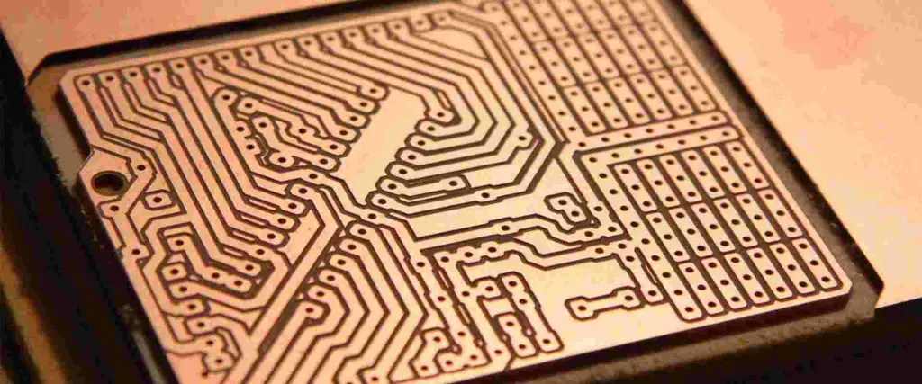
Etching is a critical process in multilayer PCB manufacturing that directly impacts the quality and reliability of the final product. While the process has been refined over decades, three major issues continue to challenge manufacturers: underetching, overetching, and uneven etching. Understanding these problems, their causes, and solutions is crucial for maintaining high-quality PCB production standards.

Overview of PCB Etching Process

Basic Principles

Etching in PCB manufacturing involves selectively removing copper from the board surface to create circuit patterns. The process uses chemical solutions to dissolve unwanted copper while protecting the desired circuit traces.

Standard Parameters

ParameterOptimal RangeCritical ValueImpact on Quality
Temperature30-40°C35°CHigh
pH Level7.8-8.28Critical
Etchant Concentration120-150 g/L135 g/LHigh
Conveyor Speed0.8-1.2 m/min1.0 m/minMedium

Issue 1: Underetching

Etching Solution for PCB

Definition and Characteristics

Underetching occurs when insufficient copper is removed during the etching process, leading to potential short circuits and other defects.

Common Symptoms

SymptomDescriptionDetection Method
Copper ResidueVisible copper between tracesVisual inspection
Short CircuitsElectrical connection between isolated tracesElectrical testing
Thick TracesTraces wider than designedDimensional inspection
Poor DefinitionUnclear trace boundariesMicroscopic examination

Causes of Underetching

Primary Factors

FactorImpact LevelPrevention Method
Low Etchant ConcentrationHighRegular chemical analysis
Insufficient TimeHighProcess monitoring
Low TemperatureMediumTemperature control
Contaminated SolutionHighRegular maintenance

Solutions and Prevention

  1. Chemical Monitoring
  2. Temperature Control
  3. Process Time Adjustment
  4. Equipment Maintenance

Issue 2: Overetching

Definition and Characteristics

Overetching results in excessive copper removal, leading to broken circuits or weakened connections.

Impact Assessment

FeatureNormal RangeOveretched ConditionQuality Impact
Trace Width±10% of nominal>15% reductionCritical
Copper Thickness35μm ±5%>10% reductionHigh
Edge Definition90° ±5°>15° deviationMedium
Surface RoughnessRa ≤ 0.5μmRa > 1.0μmHigh

Causes of Overetching

Environmental Factors

FactorRisk LevelControl Method
High TemperatureCriticalCooling system
Extended ExposureHighTimer control
Strong EtchantHighConcentration monitoring
Agitation SpeedMediumSpeed regulation

Prevention Strategies

  1. Process Control
  2. Equipment Calibration
  3. Chemical Management
  4. Operator Training

Issue 3: Uneven Etching

Definition and Characteristics

Uneven etching results in inconsistent copper removal across the board surface.

Pattern Analysis

Pattern TypeSensitivityCommon Issues
Fine LinesHighWidth variation
Large AreasMediumCenter etching
Mixed DensityHighLocal variations
Edge AreasMediumOver/under etching

Technical Factors

Equipment Considerations

ComponentImpactMaintenance Frequency
Spray NozzlesCriticalWeekly
Conveyor SystemHighMonthly
Tank CirculationHighDaily
Filtration SystemMediumBi-weekly

Quality Control Measures

Testing Methods

MethodDetection CapabilityImplementation Cost
Visual InspectionMediumLow
Electrical TestingHighMedium
X-ray InspectionVery HighHigh
Cross-section AnalysisHighestVery High

Process Control Parameters

Critical Measurements

ParameterMeasurement FrequencyAcceptable Range
Etch RateHourly35-45 μm/min
Line WidthPer Board±10% nominal
Surface FinishPer BatchRa ≤ 0.5μm
Layer RegistrationPer Board±75μm

Cost Impact Analysis

Financial Implications

Issue TypeScrap RateRework CostProduction Loss
Underetching5-8%$150/board2-3 hours
Overetching8-12%$200/board3-4 hours
Uneven Etching6-10%$175/board2.5-3.5 hours

Prevention Costs

MeasureImplementation CostAnnual SavingsROI Period
Advanced Control System$50,000 $120,000 5 months
Chemical Analysis Equipment$30,000 $80,000 4.5 months
Staff Training$15,000 $45,000 4 months

Best Practices for Issue Prevention

Process Optimization

Control Measures

AreaActionFrequencyResponsibility
Chemical AnalysisTestingDailyLab Technician
Temperature ControlMonitoringHourlyOperator
Equipment MaintenanceInspectionWeeklyMaintenance Team
Quality ChecksTestingPer BatchQC Team

Staff Training Requirements

LevelTraining TypeDurationUpdate Frequency
OperatorBasic Process40 hours6 months
SupervisorAdvanced Control80 hours12 months
EngineerTechnical Expert120 hours18 months

Future Developments

Emerging Technologies

TechnologyExpected ImpactImplementation Timeline
AI Control SystemsHigh2024-2025
Real-time MonitoringVery High2023-2024
Advanced ChemistryMedium2024-2025
Automated CorrectionHigh2025-2026

Frequently Asked Questions (FAQ)

Q1: What are the most common indicators of etching problems?

A: The most common indicators include:

  • Trace width variations
  • Copper residue between traces
  • Broken or interrupted circuits
  • Surface roughness changes
  • Color variations in etched areas

Q2: How often should etching parameters be checked during production?

A: Critical parameters should be monitored at the following intervals:

  • Temperature: Every hour
  • Chemical concentration: Every 4 hours
  • pH level: Every 2 hours
  • Etch rate: Every new batch
  • Solution level: Every shift

Q3: What is the typical recovery process for overetched boards?

A: Recovery options depend on the severity of overetching:

  • Minor: Copper plating adjustment
  • Moderate: Circuit repair techniques
  • Severe: Board replacement Note: Not all overetched boards can be salvaged.

Q4: How do different copper weights affect etching parameters?

A: Different copper weights require specific parameter adjustments:

  • 0.5 oz: 25-30% shorter etch time
  • 1 oz: Standard parameters
  • 2 oz: 40-50% longer etch time
  • 3 oz: Double etch time, may require multiple passes

Q5: What preventive maintenance steps are most critical?

A: Critical preventive maintenance includes:

  • Daily nozzle inspection and cleaning
  • Weekly solution analysis and adjustment
  • Monthly equipment calibration
  • Quarterly major system maintenance
  • Annual comprehensive overhaul

Conclusion

Understanding and addressing the three major etching issues in multilayer PCB manufacturing is crucial for maintaining product quality and production efficiency. Through proper monitoring, maintenance, and process control, manufacturers can minimize these issues and their impact on production. Continuous training and adoption of new technologies will further improve the etching process and reduce defect rates in the future.