What are the Best PCB Assembly Vancouver Companies?

Electronics Assembly Companies

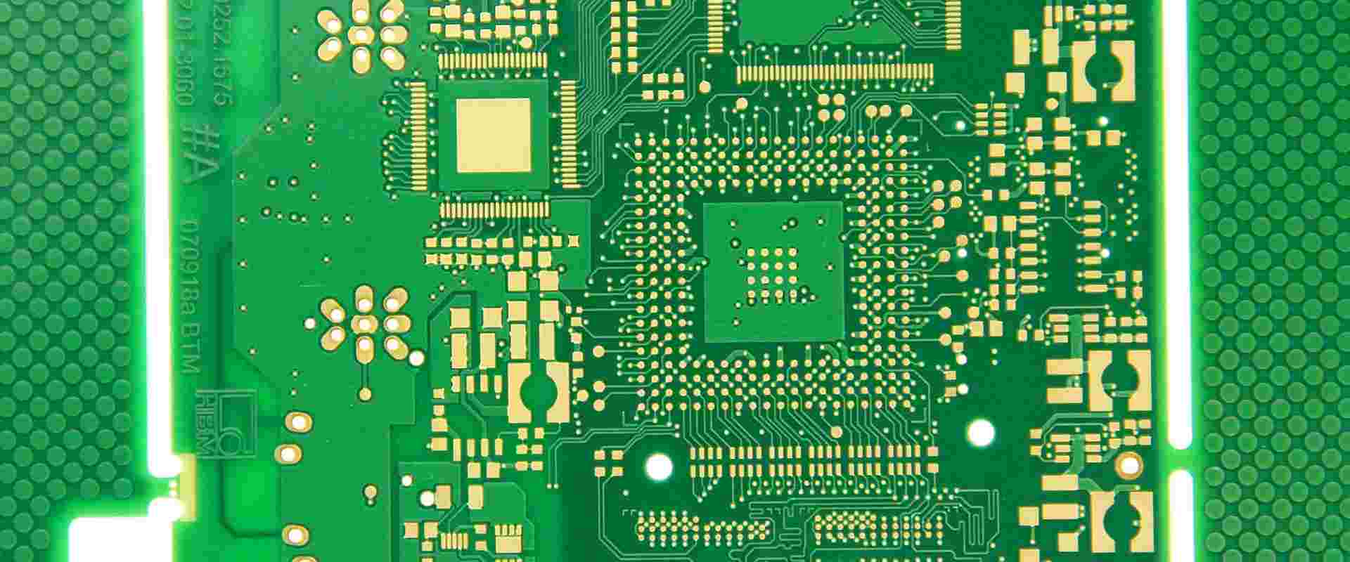
Circuit boards before assembling components are referred to as printed circuit boards. Immediately you solder the electronic components, then it becomes PCB assembly or printed circuit assembly. Different automatic and manual tools for PCB assembly are utilized for the entire process.

Furthermore, take note that there are differences between assembling the circuit board and the process of PCB manufacturing. In addition, the manufacturing of PCBs deals with different processes which includes the design and the creation of the PCB prototypes. Immediately the printed circuit board is ready, there is a need to solder passive and active electronic components onto them before it is used in gadgets or electronic equipment.

Assembling electronic components is dependent on the PCB type, electronic component type, as well as the reason behind the circuit board

Best PCB Assembly Vancouver Companies

small-batch-pcb-assembly

Maxtech Electronics Inc

This company is situated in Vancouver and is known as an EMS and PCB Assembly provider that serves all electronic assembly requirements and needs. With more than a decade of local and professional experience, this Company offers high-quality PCB assembly services to different customers all through Canada and even in the United States.

Since 2004, this PCB Assembly Vancouver Company has offered its customers its services in different industries. These include industrial controls, consumer electronics, communications, medical lighting, and automotive. Their core technical and management team combined help bring more than twenty five years of skills and knowledge in our electronics industry. They love what they do and they really want to help you build technologies that would shape our future.

In addition, this PCB assembly Vancouver Company provides different services relating to electronic assembly. Their services include mass production and prototyping, and they are flexible enough in order to accommodate all your PCB assembly needs. To achieve low-volume and prototype assemblies, Maxwell works with their customers as well as their deadlines to make sure their requirements for deliveries are timely.

Furthermore, Maxwell Electronics offers one-stop solutions. Their full turnkey PCB assembly services ensure the streamlining of your work and saves you time. This is because they will handle the procurement of the components and the PCB.

Having said this, Maxwell provides their assembly services on either turnkey or consignment basis. Asides PCB assembly, they have production technicians and tools to finish your box build.

Pronine Electronics

Pronine is an Engineering Company situated in Vancouver in British Columbia. They deal with PCB and electronic circuit design and assembly.

This PCB assembly Vancouver Company first designs your electronic circuits, because they really love it. They have efficient and elegant designs and their style is reliable and robust. Their expertise areas include mixed RF, video, audio, digital, analog signal circuits.

In addition, they have vast experience in the design and assembly of test instruments, special research equipment, detectors, amplifiers, power suppliers, motor control, and PLL synthesizers.

In addition, the Pronine offers engineering services that are outsourced for the increasing number of companies which view it as impractical to be able to maintain their personal full-time designers in all related expertise areas.

CCI Canadian Circuits

This PCB assembly company was founded in 1933 and is a top PCB manufacturer and assembler in Canada. Being involved in this for over 25 years, this company has formed the basis of the printed circuit board business.

Till today, they have been able to serve in about forty industries and boasts of having different circuit boards, which includes HDI and custom PCB. Also, CCI Canadian Circuits functions in models as well as quick turn PCBs.

Back in 2019, this Company was included among the major manufacturers and assemblers in Metro Vancouver. This is another reason why they are very strong in the field.

Omni Circuits Boards

Omni manufactured and assembled the first etched copper/aluminum bimetal trace printed circuit boards. This opened the door for other applications requiring superconducting PCBs, cryogenic temperatures, as well as chip interconnections making use of superconducting wire bonds.

Also Omni deals with the design and production of solderable and aluminum trace circuit boards that are appropriate for the aluminum to aluminum wire bonding, which are utilized by research and development groups all over the globe

Furthermore, the aluminum-trace circuit boards are utilized in quantum computing, low-temperature engineering, as well as other top applications requiring the mounting or interconnection of unpackaged chips to customize printed circuit boards.

Whether you’re interested in mono-metal aluminum wire bondable printed circuit boards or circuit board applications requiring low temperatures, this company offers a solution.

What are the Factors to Consider when Choosing a PCB Assembly Vancouver Company?

FULL PCB MANUFACTURING Quote

Check the Testing Services

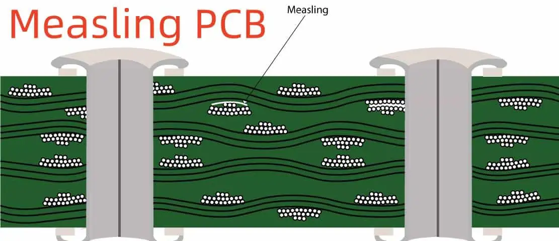
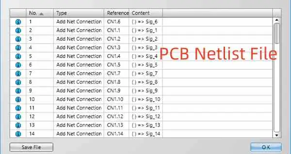
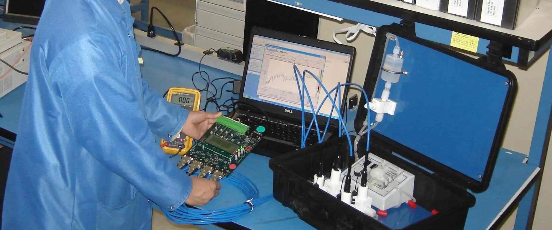
Testing is very important for guaranteeing a PCB Assembly’s quality. All quality issues could affect your business, which also ruins you. This is why when choosing a company for your PCB assembly, ask about their testing methods and procedures. Work with companies having strict control processes and comprehensive procedures for testing.

Also, in general terms, circuit boards have to pass through different inspections, which include functional testing, AOI, and visual inspection.

Learn about their services

Asides from PCB assembly, there are companies which offer other services like procurement of components, management of supply chain, design as well as other value services. Having those suppliers work with you can get rid of issues relating to communicating with several companies to get the same service.

Costs

Costs matter so much, and the PCB assembly cost is usually affected by so many factors. These include components to be utilized, the order size, costs of labor, shipping costs, etc. However, during the comparison of the different prices offered by suppliers, don’t just consider their prices; pay much attention to the quality they offer as well as other services.

Conclusion

Choosing the best PCB assembly Vancouver Company could be a difficult task. This is because there are few options available in the area, so you have very limited choices. However, expanding your options to other areas will help you make better choices and better comparisons.

In order to have a great experience as you deal with these PCB assembly companies, you may look into each company’s description, their achievement, as well as their experience to help in choosing whichever suits your needs.

What is the Function of Mechanical Layer in a PCB?

PCB Inner Layer Clearance

A mechanical layer is one of the many layers used in the production of Printed Circuit Boards (PCBs). In this article, you will learn about the function and some of the core considerations for the usage.

What is a PCB Layer?

You donโ€™t build a house without laying the foundation. Likewise, we cannot break down the concept of mechanical layer if we donโ€™t understand how the layers work in a PCB.

Layers are the levels of conducting signals throughout the circuit board. As the baseline, they provide the medium for the boardโ€™s signals to be transmitted and in the right directions.

What is a Mechanical Layer?

It is a type of PCB layer used to highlight the PCBโ€™s physical boundaries. The idea is to use the mechanical layer to point out the following:

  • The layer highlights the circuit boardโ€™s physical dimensions.
  • It is also used to show where โ€œindicative informationโ€ is to be placed in the board.
  • The mechanical layer also shows you the relevant pieces of information about the PCBโ€™s assembly and printing. Examples of the data shown are the boardโ€™s assembly instructions, the dimension lines of the board, vias information, dimension markings and the datasheets.

When to Use a Mechanical Layer

The mechanical layer is commonly used when manufacturing a multi-layered circuit board. It is also possible for the layer to be more than one. Despite the increase in the number, you must prioritize using just one layer for these reasons:

  • The basic layer, also called the Mechanical Layer 1, is used to facilitate the circuit board, by outlining the physical dimensions.
  • The PCB fabricator also relies on the mechanical layer to cut-out the circuit board from its stock material.

What is Contained in the Mechanical Layer of a PCB?

multilayer pcb stackup

The mechanical layer contains relevant pieces of information that helps you fabricate, assemble and print the circuit board. The data includes the dimension markings, information about the vias and the physical dimension lines of the board.

The mechanical layer also includes the following:

  • The specific tolerances required for the PCB.
  • The dimensions and overall profiles of the circuit boardโ€™s contour.
  • The mechanical layer data file also includes the sizes and positions of the cut-outs and internal slots of the board.
  • The special build requirements and drill map can also be included.
  • The reference hole and layer sequence are also added.
  • Customer panel and;
  • Drill position symbols

The Altium Mechanical Layers

If you are using the Altium Computer-Aided-Design (CAD), there are certain processes to adding the mechanical layers.

Classifications of Altium Mechanical Layers

Altium supports two (2) types of mechanical layers. These are the pair of layers and individual mechanical layers.

On the one hand, the pair of layers are used for such tasks, such as component courtyard. These layers are primarily used for component-related details, and apply to one side of the PCB.

On the other hand, the individual mechanical layers are the ones used for tasks that do not directly to a specific PCB side. This is why you can use these layers for the circuit board outline.

The Individual Mechanical Layers

Different kinds of properties are included in the Altiumโ€™s individual mechanical layers. These range from the shape of the PCB to the route tool path and the assembly notes.

Here is a breakdown of the different properties you can find inside the individual mechanical layers on Altium Designer:

  • Sheet: this mechanical layer is used for defining the outer document drawing template border.
  • Assembly Notes: these are the layers used for highlighting the relevant instructions for assembling the circuit board. The assembly notes can also be used to define the componentsโ€™ load.
  • V Cut: this defines the โ€œV Cutโ€ details, which are used to divide the PCB. For this to happen, this layer is used to make a โ€œV-like grooveโ€ at the boardโ€™s bottom and top. Afterwards, a minimum amount of material is left in place to hold the PCB panels together.
  • Board and Board Shape: while the โ€œboardโ€ refers to the highlighting the board-related instructions; the โ€œboard shapeโ€ highlights the overall presentation or outline of the circuit board.
  • Dimensions: this mechanical layer defines the dimensional details required for the PCBโ€™s production.
  • Route Tool Path: this mechanical layer contains details for the circuit boardโ€™s mechanical routing.
  • Fab Notes: this layer contains important pieces of information about the boardโ€™s fabrications.

Component Layer Pairs Mechanical Layer

This refers to the pair of layers used for component-related details. The following are some of the properties:

  • Courtyard: this layer defines the space required for placing the component on a PCB. In addition to specifying the space for the component placement, the courtyard also specifies the collision detection, component selection and the componentโ€™s area.
  • 3D Model: this layer is used for making a Three-Dimensional (3D) representation/outline of the circuit boardโ€™s component.
  • Designator: it is used in the assembly drawings requiring component designators. This layer is primarily used for placing the .Designator special string on the PCB.
  • Gold Plating: this component layer highlights the requirements for making a selective gold plating.
  • Coating: this layer highlights the PCBโ€™s component areas that require protective coating.
  • Component Outline: this is an Altium board outline mechanical layer used for representing the mass that the electronic component occupies on the circuit board.
  • Assembly: this layer is used to draw the assembly data for the PCB component.
  • Dimensions: used for defining the componentsโ€™ dimensional details.

Differences between the Mechanical Layer and the Keep-Out Layer

Have someone ever tried to cross your boundary and you are forced to install a โ€œkeep away from hereโ€ sign? This is a good way to establish a boundary and something similar can be seen in the PCB industry.

There are a couple of differences between the mechanical layer and the keep-out layer and the major one has to do with boundaries.

1.    Boundary Specifications

The mechanical layer is used to specify the physical boundaries or physical dimensions of a circuit board. However, the keep-out layer is used to restrict the layers within a specific (working) area.

2.    Who Uses the Layers?

Since the mechanical layer specifies the boardโ€™s physical dimensions, it is given to the fabricator. However, the fabricator doesnโ€™t always use the keep-out layer. Rather, the keep-out layer is โ€œfedโ€ into the PCB design software. The goal is to help the circuit board designer to follow the existing dimensions and never have to step out of the โ€œboundariesโ€ when designing the board.

3.    For Mechanical Clearance Purposes

The keep-out layer can also be used to enhance the mechanical layers functions. For example, it can be used to identify the internal segments of the circuit board that need to be cleared off the path for mechanical reasons.

Other Types of PCB Layers

Besides the mechanical layer, there are a couple of other layers that enhance the performance of a Printed Circuit Board (PCB).

Routing Layers

These are both internal and external PCB layers, because they can be found both inside and outside the circuit board. The routing layers are used to make an interconnection of the boardโ€™s components.

Solder Paste Layers

Primarily used with the Surface-Mount Devices (SMDs); the solder paste layers are used for solidifying the bonding of the solder paste with the PCB components.

The solder paste layers are also used because of the way they increase the flow of solder in the board.

Solder Mask Layers

These refer to the layers containing the protective coating or mask on a PCB. The mask is called the solder mask.

Typically green in color, the solder mask layers help to protect the top and bottom of the circuit board from contamination and damage.

Silkscreen Layers

These include the top and bottom overlays and are used for placing the texts of the PCB components. With the silkscreen layers, you will be able to identify the profile of the circuit boardโ€™s components, as well as the number of components on the board.

The Ground and Power Planes

These layers are usually connected to an onboard voltage point and are used to boost the PCBโ€™s performance, under specific conditions.

The ground and power planes also oversee the distribution of power and ground across the components, as well as been positioned within the bottom, top and internal parts of the circuit board.

Best Practices for Mechanical Layers in a PCB

FULL PCB MANUFACTURING Quote

To be on a safe side, here are some of the best ways to maximize the use of mechanical layers in your circuit board:

  • It is better to make an outline of the board by using a small line that measures 0.5mm wide. The center of the line represents the circuit boardโ€™s outline.
  • The actual milling layers of the circuit boardโ€™s contour should not be provided. Those of the cut-outs or internal slots should not be provided either.
  • The mechanical layer must not be rotated or mirrored.
  • The mechanical layer must always be a 1:1 and always represent the PCBโ€™s actual dimensions.

Final Words

The mechanical layer provides the guideline for producing the PCB in the right dimensions. Always ensure to use the 1:1 ratio, never scale the layer, and create the outline on time.

What is Measling PCB & How Can It be Avoided?

Measling PCB

Measling in PCB refers to the discreet white spots that appear on the circuit boardโ€™s base material. In this article, you will learn more about it and how best to avoid it.

The Meaning of Measling in PCB

Measling is a term used to describe the occurrence of white, discreet spots in the base epoxy-glass laminate of a PCB. The inappropriate application or resin to the circuit board is a major reason for the occurrence.

Why Does Measling Occur in a PCB?

Besides the inappropriate resin application, measling also shows up in the circuit board due to other reasons.

One of such reasons is the inconsistency in placing the layers in the board for accurate bonding. This is sometimes a โ€œmanufacturer problemโ€ and can be mitigated if the PCB manufacturer pays an extra attention to how the layers bond together in the boardโ€™s stack-up.

The other cause of PCB measling is the hydroscopic nature of the Flame Retardant 4 (FR-4) material used for PCB production. To this end, the material sometimes, absorbs water vapor from the air. This, in turn, excess moisture will be stored only to be turned into measles when a heat source, such as soldering iron or reflow oven is used.

Is PCB Measling Destructive?

The presence of white spots in the PCBโ€™s interior (measling) could be โ€œdestructive.โ€ If not well-managed, it could culminate in degraded physical and electrical performance of the board.

Let us look at just how far the destruction can go on.

The Tolerance

While measling can change the exterior design of the board, it can also be tolerated. Small amounts of measling can be tolerated, but must be managed to prevent further spreading.

When Does Measling Occur in a PCB?

Although measles occurs when the resin is not properly applied, it can also occur in other cases. For example, a lowered surface finish increases the boardโ€™s exposure to measling, as it reduces the boardโ€™s chances to resist measling.

It also occurs when there is excess mechanical stress in the PCB. The fact is that measling tends to occur at least, once in the lifetime of a Printed Circuit Board (PCB).

How to Evaluate for Measle-Related Defects in a PCB?

How do you test for measling in a circuit board? Here are some tips:

Laminate Exposure to Moisture

This is a special technique to evaluate measling in the PCB. The process involves:

  • Exposing the PCBโ€™s laminate to moisture. This must be done prior to the immersion or dipping to the solder paste.
  • The next step is to immerse the laminate inside a hot solder paste, which must be up to 500 degrees Fahrenheit.

Etching and Solder Processing of the Laminate

The previous method is used to evaluate the circuit boardโ€™s compatibility. The next step is to subject the laminate to etching and processing.

Note: the etching and solder processing of the board must be followed soon after the laminateโ€™s exposure to moisture. However, you must desist from this process if the board didnโ€™t pass the exposure to moisture. This way, you will reduce the chances of further population of measles on the PCBโ€™s surface.

PCB Measling Preventive Measures

As much as small amounts of measling can be tolerated, it is always best to avoid it. Here are some tips on how to go about it:

Be Careful with PCB Baking

Baking a PCB is always recommended, because it involves the use of heat to facilitate the removal of excess moisture in the board.

It is always recommended to use a temperature of between 100 and 105หšC to bake the board. However, you must be careful the way you go about it.

Sometimes, PCB baking can trigger a chain of issues, such as inaugurating solderability into the circuit board.

It is therefore, recommended that the baking process should:

  • Be heated between 4 and 6 hours.
  • Only be done when necessary. That is, when excess moisture is trapped inside the PCB.

Here are additional suggestions on how best to avoid measling in your circuit board:

  • Always work with a professional circuit board manufacturer who will use the right methods to reduce measles in the PCB.
  • Follow a laid-down procedure for circuit board procedure.
  • As a way of preventing the boardโ€™s exposure to moisture, consider using moisture-resistance bags for the PCBโ€™s storage.
  • An accurate temperature must be maintained on the board before it is subjected to thermal processing.
  • Resin-control methods should be used to prevent measling in PCBs.
  • Always store the PCB in a dry place.

PCB Measling vs. PCB Delamination

FULL PCB MANUFACTURING Quote

Measling and delamination are two different terms used to suggest a similar problem โ€“ the presence of defects in a PCB. While they might seem similar, some differences exist between the two.

Delamination in PCB refers to the partial separation in the circuit boardโ€™s base materialsโ€™ layers. When this occurs, blister-like bubbles or gaps are created.

The causes of delamination in a PCB include but are not limited to:

  • The exposure of the base materialโ€™s laminates to humidity.
  • Loosing of the resin from the laminate or foil.
  • The loosing of the resin from fiberglass either from humidity or heat.

The differences between PCB measling and delamination include:

  • Measling has to do with the formation of white spots on the PCBโ€™s interior, while delamination refers to the partial separation of the boardโ€™s base materialsโ€™ layers.
  • Little amounts of measling can be tolerated, but delamination can impair the boardโ€™s functions.

What Happens if Measling Cannot be Controlled?

There is also a possibility that measling might not be fully-eradicated from the Printed Circuit Board (PCB). In such a case, what do you do?

Here are some options worth exploring:

  • The board may still be able to function optimally, especially if the affected (measled) areas on the board do not stretch from two traces of from through-hole to through-hole.
  • Ensure the quality of the inner layersโ€™ oxide layer by storing the boards in a dry place.

Conclusion

PCB measling doesnโ€™t pose much of a challenge, provided the affected areas do not stretch beyond two traces. If that is the case, you can expect the PCB to short-circuit.

For excellent management, always work with a professional PCB manufacturer who will manage the process better.

Eagle Schematic: How to Create a Project and Start

EAGLE PCB

Eagle is a popular PCB design program that offers different features for enabling efficient PCB design process. This PCB design software program is often preferred among PCB designers because of its reasonable limitations. The user interface of this program allows you to select a mode and carry it out several times.

You can easily create and start a project in Eagle. Creating a schematic is important for your project. It is an important aspect of PCB design that specifies parts and which pins you need to connect on the parts. Here, we will teach you how you can create a project and start a schematic in Eagle 6 or 7.

How to Create a Project and Start a Schematic in Eagle 6 or 7

schematic-eagle
  • Visit the Eagle control panel and open the โ€œProjectsโ€ branch. You will get to see some sample projects. There are yellow icons which indicate simple directories while the red icons are project folders.
  • Click on the project entry and the context menu will pop out and display the โ€œNew project.โ€ You need to name your project and press the Enter key to confirm it.
  • After this, a new project would have been created using the name of the project. This project already has a file called Eagle.epf in which all the settings during the entire project will be stored. There is a green marker which shows if the project is active. You can click on the project folder entry and choose Edit Description if you need to include a description for the said project.
  • You can now input your descriptive text at the windowโ€™s bottom part. Based on your desire, the HTML tags can be used to format the text. You can as well include links to web locations or images.
  • It is time to design a new schematic. Click on the project entry and choose New/Schematic. You will see the Schematic Editor window displayed. The first thing to do is to position a drawing frame which is available in the Frames. Ibr. After this, make use of the icon โ€œADDโ€ to place frames or components in the schematic. You will see the ADD icon on the toolbarโ€™s left side.
  • Select an icon and you will see a display of a window with all libraries. Go through the list and check for the frames. Choose one of the frames you want. You can now place the frame in the schematic.
  • There is an ADD command which helps you in placing components. You will see a Search line at the ADD dialogโ€™s bottom. Here, you can input the name of the part.
  • Before you begin creating the schematic, there are two vital things you should be aware of. These are:

The setting of the default grid in Schematics should be 0.1 inch. Ensure you keep the setting of this grid as all Eagle schematics symbols work according to this grid. You can decide to set the grid to in millimeter which equals to 2.54mm. However, ensure the size of the grid is unchanged. The size of the gird in the schematics doesnโ€™t determine the size of the grid in the layout.

Ensure you select the Display ICON and go to layer 93 where you can be sure of where you need to connect the pins of a symbol with a net.

  • On the schematic editorโ€™s left side you will see an icon toolbar. Over it, there is an icon that displays the name and functionality of the toolbar. You can navigate the icons. Check the help function to know more about some commands you canโ€™t use.
  • The SMASH command is one of the interesting commands you will like to explore. It shows value text and name from a symbol to change its size.
  • The Electrical Rule Check is the last step to follow when you are creating Eagle schematic. You will see the outcome of this check in the Errors window. Check the warning and error messages on the screen. Eagle will direct you on where to check for the drawing. Ensure you carefully read the messages to know what to do.
  • The problem outlined in the message may be okay for you in some cases. Therefore, you need to approve the message.
YouTube video

What Functions Does Design Rule in Eagle Schematic Offer?

The Design Rule Check (DRC) evaluates or assesses the designed board against some rules in order to detect any error or issue. Although it isnโ€™t perfect, it can help in detecting some common mistakes. Below are some descriptions of all tabs in this aspect:

  • File enables you to select the DRC file you want to use. Some groups already have a particular DRC file. Therefore, you might want to use one of them.
  • You can add Layers by transforming some things in the Setup. The Layers tab isnโ€™t readily available in the freeware version. However, you can explore this tab if you are working with one of the paid licenses.
  • Clearance informs Eagle about the space you need between the electrical contacts on a circuit board.
  • The Masks layer designates masks on the PCB. During the fabrication of a board, there is a coating that protects the board. If the PCB is assembled by a machine, solder paste is applied and a stencil is created. Stop helps to control the size of the holes in the stop masks for the different parts while Cream controls the hole size in the stencil.
  • The Distance tab shows the distance between routing and the circuit boardโ€™s edge. Hole or Drill is the calculated distance from a routing to a drill in the PCB.
  • Shapes enable the creation of pads with rounded edges.
  • The Size tab allows you to choose whatever size you want your smallest drill to have. Always set the minimum sizes. You can get the minimum width from your fabrication house.
  • Restring regulates and monitors the size of vias and through-hole pads.
  • The supply layer gives control over thermals.

How to Add Parts to Eagle Schematic

FULL PCB MANUFACTURING Quote

Eagle schematic design requires you to add parts to the schematic sheet. After which you have to wire the parts together. However, you can carry out the two steps interchangeably. This means you can add a few parts and wire some parts.

The ADD tool

This tool is what you need to place components on the schematic. The ADD tool shows a library navigator. You can expand some particular libraries and check the parts it holds via the library navigator. Furthermore, there is a search functionality in the ADD tool. It helps in navigating through many libraries to locate a part.

Add a frame

You need to add a frame as it makes your schematic appear neat and organized. After you have chosen the part you will be adding, it will begin to hover around. Just left-click to place the part well. The add tool will always act like you need to place another part after you have successfully placed a part. You can exit the add-mode by clicking on the ESC button twice. Alternatively, you can choose a different tool.

Save

The schematic is not yet saved. Therefore, you need to click on File and choose save. Ensure you give the schematic a name you desire. The title of the frame will update immediately after saving.

Add the power input

After this, you will include different parts. Make use of the add tool for this step. The MOVE tool will help you to move your parts.

Add the main component

You need to include the main component and some other components. Choose one of the options on the rotate toolbar so as to rotate parts as they are being placed.

Add the connectors

This step involves adding some connectors.

Tips and Tricks in Eagle Schematics

Verify connections

There is a SHOW tool that helps you confirm the connections of all pins across the schematics. Once you use this tool, all the connected pins will light up.

Names and values

Each component on the schematic must have a value and a name. The value enables you to describe some distinct characteristics of the part. For instance, you can describe the capacitance of a capacitor. On the other hand, the name helps in identifying each component on a schematic.

Copy and paste

The Copy and Paste tools in Eagle function in a different manner. In Eagle, Copy carries out copy and paste functions. Once you copy a part, you will see an exact copy waiting for placement. The Paste is only used for pasting a group that was already copied to the clipboard.

Conclusion

It is very easy to create and start a project in Eagle Schematics. Eagle as a PCB design program offers the best tools for creating your schematics. This process is a very simple one if you follow the right steps.

Significance of a Netlist PCB in Electronic Design

PCB Netlist

A netlist PCB has several uses. At different phases of the electronics design process, PCB netlist serves many purposes. The fact is that netlist can have distinct data formats, but they offer similar functions. The Netlist PCB provides a list of connections in a circuit. Therefore, the netlist is crucial for different tasks in PCB layout and electronics design.

Netlist lay out every component and their connections on the circuit board. You can use a netlist in your schematic editor and also your PCB layout editor.

What is a PCB Netlist File?

To understand what a netlist file is, you need to know what the term โ€œnetโ€ is. Net is the link between two or more components. The components will be placed on the PCB. Therefore, you can refer to a net as group of resistors, capacitors, and resistors that concerns analog simulation tools. A PCB netlist is therefore,  a text that describes components and their connections.

Every netlist comes with a list of parts and their PINs, designators, and keywords for reference and context. Generally, netlists differ in terms of the amount of details they provide and their formats. PCB netlists are useful when testing a board. With this document, engineers can perform tests to identify any missing or incorrect connections.

Furthermore, they give instances and reveal certain properties of the components involved. PCB netlists are usually different when it comes to their complexity and structure. However, they provide the same function in electronic design. PCB designers as well as engineers have a good understanding of the significance of Netlist in PCB creation. A netlist doesnโ€™t only help to detect possible errors, but also helps to make adjustments.

This document is quite easy and simple to understand even if it is your first time seeing this format. In a netlist, you will see parts list that informs you what every designator means. It is important to know how a netlist is interpreted as it helps to troubleshoot some mistakes. These mistakes may occur due to the use of netlists from other libraries.

You can modify a netlist for some reasons. These include changes in pin number, special characters, and redundant net names. Also, any changes made to a netlist must be well documented.

What is Netlist in PCB Design?

PCB Netlist File
PCB Netlist File

There are several cases where a netlist has proved to be useful during PCB fabrication. Before you begin editing, a netlist is crucial. The program reads the Netlist during the loading of the Gerber data transfer file. After this occurs, the components are logically organized from the top to bottom. Gerber creates another netlist after the program has given each type a layer.

A gate level netlist enables designers to discover and correct any discrepancies in the file. Therefore, it is crucial to identify the divergence from how things must be. When performing CAM testing, a netlist file will always stay active. Another netlist check is performed to identify any electrical shorts and openings that are likely to happen. CAM will design a file for one the electrical test fixturing methods of the next stage.

How to Import Altium Netlist

Sometimes you will need to design a board which a different software package has been used for creating its schematic. Since there is a PCB layout designed by a netlists, most people ask if we can use the inputs from other systems. Is it possible to begin a layout without having a schematic? Yes, it is.

In Altium, an ASCII netlist can be imported and the layout can be performed without synchronization. The Altium User Forum gives a description of this process. It can be stressful to keep up with changes in a circuit along the way. However, Altium has looked for a better way to make things easy.

There is โ€œImport Wizardโ€™ is capable of working with different types of design files. This was developed by Altium as an alternative to importing a netlist.

Altium can make things easier for users and minimize the risk of mistakes. Is it possible to export a netlist from the other direction? Yes, it is possible to do this. In Altium netlist export, you can take advantage of other design files.

Other Types of Netlist

In the PCB manufacturing process, there are other types of netlist. These are the IPC netlist and the Gerber netlist.

The IPC-D-356 netlist

The IPC netlist compares schematic netlist with Gerber data before the PCB manufacturing process. This comparison checks for any discrepancy. Your NRE charge will increase if you request this test. However, it is a good decision as it will save more costs rather than producing bad boards. This will even be worse if the error is detected after final assembly.

To perform this comparison, you need to include netlist testing to your quote. You should as well have it in mind that the test will occur before manufacturing the board. Any discrepancy means the PCB manufacturing will be stopped to solve the issue.

Gerber netlist file

When you use the ODB++ data format to send your design, there will be netlist in the package. The CAM department usually obtains a netlist file from the Gerber Data. This file will be used for the PCB test.  There is always the addition of NRE costs when you receive a quotation from your supplier. These costs are one-time costs. In order to compare the finished bare board manufacturers obtain a netlist file from the Gerber Data.

With this, they can confirm if the final PCB connectivity corresponds with the input data that was sent.

What are the Causes of Discrepancies?

Errors could occur in Gerber files since they are not infallible. Features that are not correctly described can make the system to misinterpret data. Examples of incorrect features are unfilled polygons or incorrect-sized pads. In some cases, a self-intersecting polygon will incorrectly resolve. Hence, this makes the polygon fill to leak.

The best possible resolution is to export Gerber files. Alternatively, you can opt for line fill rather than polygons. However, it is advisable to provide a netlist. Furthermore, a CAM program can misinterpret some things due to operator setup errors. The CAM system can see otherwise if a positive plane is assigned as negative. Therefore, the netlist will not be accurate.

In order to reduce the possibilities for operator error, you can provide positive polarity for internal layers. The best thing to do is to provide a netlist file with other Gerber files. Review the polarity assignments and layer type if there are multiple opens or massive shorting.

How do PCB Manufacturers use Netlist?

When reviewing a PCB design, the PCB manufacturer compares the data in the schematic netlist against the BOM, schematic data and Gerber. Discrepancies do occur between a netlist and some of these documents. In most cases, this is a result of exporting a BOM and netlist before the completion of the design.

Furthermore, PCB manufacturers make use of netlist to specify the requirements for testing a bare PCB . In this case, the manufacturer programs the connectivity in the netlist into the test fixture. A suitable format is the ODB++ data file format. This is because you can generate the netlist from the package.

There are several software programs you can use to generate Netlist. Asides from Altium designer, Cadence Allegro and KiCAD are good pieces of software you can use. The Allegro netlist and netlist KiCad are preferred among PCB manufacturers.

What is the Difference Between a Netlist and a Schematic?

FULL PCB MANUFACTURING Quote

Netlist in PCB design offers a structure for describing connections among components. It always comprises signal keywords, reference designators, and more. A PCB netlist offers you the vital elements to achieve a great design without errors. Netlist helps PCB manufacturers to verify a design. That is why manufacturers love to get the final netlist in order to fabricate the PCB according to specifications.

On the other hand, schematics provide necessary details about all nets and components a circuit board design. It makes it very easy to read and understand circuitry. One of the benefits of a schematic is that it defines the links between component symbols. A schematic is a visual representation that describes the connectivity of a PCB design.

With a schematic, you can identify parts and components by using designations. Many PCB designers use netlist integration, custom editing is necessary due to the various formats of netlists. Design teams may need to include extra documentation due to how complex some schematics can be. This documentation is a description of the design functionality. Both netlist and schematic are a great tool for providing information as regards PCB design.

Conclusion

A netlist PCB provides crucial information sources for the electronic design process. With this document, PCB designers and manufacturers can determine the functionality of a circuit board. The data in a Netlist helps to gain easy reference to everything happening. When there are some errors, the Netlist would reveal them and fix them.

A PCB Netlist is very useful for every phase of the design or testing process. It is difficult to detect errors and how to fix them without having a netlist.

PCB Functional Testing Vs. PCBA Functional Test

Hardware Testing Engineer

PCBs are now an important part of our consumer electronics. These are highly crucial for the fine performance of our devices so that our lives can be at ease. PCBs need an extensive production process that involves various steps. However, the production of PCBs is not enough. The testing of PCBs also matters here. It comes in handy to rule out defective PCBs and deliver industrial-grade PCBs to the users.

These testing methods basically enable the technicians to check if the PCBs are functional and safe to use. Or else a damaged and defective PCB can ultimately ruin the whole electronic device in the future. We are going to have a detailed look at the testing of PCBs so that you can easily learn about it through our post. Letโ€™s get on with it!

YouTube video

Common Functional Testing Techniques

One of the most common methods is functional testing, aka FCT. If you do FCT, precisely meeting all its requirements and executing on the basis of its guidelines, it will help you test your PCBs on a deeper level. Now FCT is for testing each component individually. An FCT test is also reliable for the verification of the optimum atmosphere for the PCBs. In the end, the results of this FCT will give you a clear knowledge and idea about the health of your PCBs. Such tests are important in the domain of PCBs, where producers are able to produce exceptional PCBs for the users.

There are some tools that you need to do this test:

  1. Monitors
  2. Cables/wiring
  3. Connective interface
  4. CPU

Factors affecting FCT: 

fct functional circuit test

When we consider FCT, we need to have some factors in mind so that we can drive positive results. The factors affecting FCT are:

  1. How much area of a PCB undergoes testing
  2. What type of results are needed
  3. What is the type of input and stimuli
  4. Which parameters are under consideration

Read more about:

The correct way to do FCT:

By far, you have a clear idea that FCT is important for PCBs. There is no margin of negligence since it can alter the results. In FCT, the goal is to analyze and test all the components. There are also other alternative methods that you can use in place of FCT. However, if you are going for FCT, you need to do it in the correct way. In this section, letโ€™s talk about the accurate method of doing FCT on PCBs!

Test Procedure List Creation

You need to properly plan the FCT procedure so that each and every PCB part undergoes testing. Or else hidden defects create future problems in most cases. You need to write down all the methods that you are going to opt for in this process. Also, what PCB parts will undergo testing? Make a list and stick to it till the procedure ends. It is an expert recommendation and comes in handy for the desired results.

Letโ€™s see what PCB parts need proper testing: 

  1. ResistorsResistors are important to the current transmission that basically gives power to the PCBs. A multimeter is a good option when you want to test the resistors. Make sure to get proper readings and analyze your results on that basis. 
  2. Sensors: These are for working with the environmental changes around them, and due to this, they produce electrical signals based on these changes. A multimeter is beneficial to test a sensor and identify its defects. 
  3. CapacitorsThese are for controlling the electric charge or voltage in a device or PCB. You can also test the capacitors to see if they are working just fine for your devices or not. 

Voltage Meter Testing

PCB E-test machine
PCB E-test machine

The correct voltage holds great importance in the fine performance of PCBs. Changes and problems with the voltage create a negative impact on PCBs on the whole. The voltage and power work together in a PCB to make it work. In case you are using low voltage and high-voltage, you need to always test it. So that it will make your PCBs much safer to use, to test the voltage, you can use a voltage meter. The reading of the voltage meter is for indicating the performance of the voltage. Later, you can also determine the performance based on the voltage readings. 

Load Testing

The loads are an important part of PCBs because they help them fight against unfavorable conditions. Also, loads endure pressure and strain, which greatly helps PCBs in performance. When we test a load, we want to make sure it endures pressure and strain to a large extent or not. However, the result of the test can vary as to the following factors. These are:

  • Temperature: Temperature is also important for PCBs. In case of overheating, the PCBs can melt down and undergo full failure. The materials used in the board basically determine its temperature. Therefore, while testing the load, you need to maintain the temperature on all counts. 
  • Current: The current changes can also alter the results. Therefore reading the current precisely is important in load testing. It will help you verify the performance of PCBs on the whole as well. 
  • Operating frequency: PCBโ€™s operating frequency also needs your attention. The PCBs usually work with high frequency and low frequency since there is no in-between. When you do FCT, you can deeply check the operating frequency as well. 

QC Testing

QC testing is another important type of PCB testing method. It helps you know that the PCBs are of industrial grade and meet industry standards as well. This test is basically for the verification of the final product. These are different from FCT since it does not test the final product. The QC test verifies the PCBs on a deeper level. From their design to components and performance, a QC test will give you all the insight about your PCBs. QC tests also rule out defective PCBs and highly hidden defects in PCBs so that they will remain intact and safe to use in consumer electronics. Defective PCBs are not only harmful but also can lead to loss of money by ruining the entire electronic device in the future. 

Why Testing Is Crucial and How It Matters to You

Now we are going to see the major benefits of FCT and other PCB testing below:

  • Power issues: PCBs need a stable and consistent supply of power to perform nicely. With the PCB tests like FCT, we can make sure that PCBs are getting the optimum amount of supply. It prevents chances of mishaps and problems. 
  • Signal distortion: Tests come in handy to identify the signal distortion and treat it in time to avoid major setbacks. 
  • Inaccurate voltage: Some PCB tests, like voltage testing, makes sure that the voltage supply is accurate and that there are no issues with it. It detects voltage issues in real-time so that you can make the changes successfully

PCBA functional testing

The PCBA is a type of PCB testing method that is normally for testing complex circuits and PCBs. Now any negligence in doing the PCBA can falsify the results. Also, any human error can change the results, which is not acceptable, however, despite the fact that PCBA is a powerful testing method. In some cases, it can leave some defects hidden. Therefore pairing PCBA with FCT and ICT proves to be beneficial in analyzing the PCBs intensely. 

Benefits of PCBA Testing

PCBA testing is beneficial for detecting life-threatening faults in PCBs to save the life of users. In case of short circuits and current leaks, the users might face an irreversible situation. Therefore, it is important for a PCB producer to rigorously test the PCBs before delivering them to its clients to ensure their safety on all counts. Plus, doing the PCB tests in time will give enough room to reverse the faults and defects before delivering. 

Most Popular PCBA Testing Methods

FULL PCB MANUFACTURING Quote

We have picked some popular PCBA tests: 

1.         Visual Inspection

VI is mainly for detecting the issues with PCB soldering. It is a basic PCB testing method in which you will analyze the PCBs with the naked eye without using high-end equipment and machinery. It is not good for detecting small PCB parts. Only big and visible solder joints can undergo visual inspection. However, skills are needed for visual inspection and to drive positive results from it. 

2.         Flying Probe Testing (FPT) 

The FPT is an affordable testing method and useful to replace the ICT, which is an expensive option. The probes basically identify the PCBs by penetrating through them and only test special areas on the board. It is easy to conduct as well.

3.         Burn-in Testing:

This method is intense as compared to other PCB testing methods available. It exerts extreme stress on the PCBs. Now, problems can occur during burn-in testing. It can include catching fires, overheating, and damage to the PCBs. However, if handled professionally, burn-in testing shows great results. There are some downsides of this testing, including risks of PCB damage, overheating, and high price. 

Functional testing (FCT) 

An FCT is highly beneficial for the performance of PCBs. It rules out small to big PCB defects impressively. Moreover, it normally takes place at the end of the PCB production. It is also affordable, which means many PCB producers can do this test to ensure the quality and performance of their PCBs. However, skillful workers are important in order to get desired results from FCT. It is a much less rigorous test and might still leave some defects undetected. 

Raypcb As Your Contractor’s PCB Testing Capabilities

If you ever get confused between the PCB tests, then RayPCB will help you. We will analyze your PCBs and recommend suitable tests for them. Therefore before making any decision, it is important to seek professional assistance to avoid future complications. 


What are the Functions and Applications of Spring Loaded Pins?

Spring Loaded Pins

At times, thereโ€™s a need for electrical connections to become solid, however, temporary. Or, it could be subjected to much vibration in order to undo what was done; or, you will have to break or make many connections all at once throughout the board.

For these cases, these usual combinations of cables, plugs, and sockets might not be appropriate. This is why we may consider making use of spring loaded pins or spring loaded pin connectors.

Properties of the Spring Loaded Pins

For our connections, the spring loaded pins could bring these properties:

  • With pressure, you can create or break multiple connections at about the same period and across a very large area. These are useful for the testing jigs like bed of nails which have to connect, test, and disconnect quickly.
  • Also, they need a soldered component on just one of both boards. Most times, this board is one which is not mass-produced. Furthermore, its mating side will only require a minim pad at just one place. This helps in saving space, cost, as well as the routing area.
  • If it is chosen and well-designed, they could work in environments having vibration
  • These compressed connections could be vertically compact; boards could be stacked close to themselves
  • With springs, you have height flexibility, which is useful in cases where there are staggered board stacks or uneven boards.

It is very useful; however, anyone who has made an attempt to spec the spring loaded pins knows fully well that there are lots of combinations to select from. These include material, tip geometry, diameter, height, plating, material, height, housing, force, and more.

In this article, weโ€™ll be focusing more on those features, which relates to compatibility with manufacturing and placement of automated components.

Get it Right

Spring Loaded Pin
Spring Loaded Pin

First, you need to know that electrical connections must be reliable and robust. Also, spring loaded pins have to be placed at an appropriate angle. In addition, they have to be properly aligned with the contactโ€™s center found on the opposite side, and not buckle, bend, or become unaligned with pressure applied.

There is a need for the contact pad found opposite the pin to be large and flat enough to be able to account for the alignment vibrations and mismatches, and plated in a way that this contact does not degrade with time and use.

As we know, the placement of the component could be done making use of the automated pick and place machine or manually done. The pick and place is usually cheaper for the high component boards. Therefore, ideally, we try to select components that work well with the process. Whenever we refer to the spring loaded pins, thereโ€™s a need to have caps that sit on the top of every discrete pin or on just a subset of these pins in โ€˜housedโ€™ connector arrays. The pick and place head grabs this cap for placement.

Also, they need to come in a specific packaging that works well with the pick & place machines. These include tape, tube, tray, reel, etc. When delivered in โ€˜bulkโ€™ or โ€˜looseโ€™, the assembler would have to manually place them into the pick and place feeder or solder them by hand, and end up charging you for additional work done.

Addressing Stability and Alignment

Here, we will be addressing stability and alignment. Below are some properties to take note of.

Through hole or surface mount

The through hole for the spring loaded pins is at times referred to as a โ€˜tailโ€™ that offers a solid solder stability and joint.

Connector or single array

The single pins, most especially those having no housing can easily experience as well as stability problems during assembly and use respectively.

The connector arrayโ€™s configuration

One row might experience the misalignment whenever it is soldered. Therefore, a reliable choice would be the 2 x 2 array and larger. Therefore, when you have to choose between the 2 x 3 and 1 x 6 configurations, the former is better.

Proportion of the base area to the length

When a pin is longer, the base area would be smaller. With this, there is a greater chance for unreliability and misalignment. Defining its โ€˜lengthโ€™ is difficult. However, you should pay attention to this, most especially the surface mount pins.

With respect to stability and alignment, the most appropriate spring loaded pin is through hole, with its โ€˜tailโ€™ as short as possible, as well as arranged in a larger configuration or housed 2 by 2. If you wish to use the surface-mount or long pin, most especially the single pins, then you have to first consult the assembly house to know if they encountered any problems given their equipment and process.

Lastly, make sure you work with instructions of the manufacturer regarding assembly, as well as reach out to them when choosing the most appropriate variant for your applications. This helps you make the best decision especially when there are lots of parameters and options available.

What are the Applications of the Spring Loaded Pins?

FULL PCB MANUFACTURING Quote

Board to Board

Spring loaded pins are a requirement for board to board connections between at least two boards. You can stack these boards on themselves using the spring movement. This helps to accommodate misaligned boards, tolerance stack-ups, as well as errors found in co-planarity and parallelism.

You can accomplish this in different ways making use of the spring-loaded pin. Whether these boards are perpendicular or parallel, horizontal or vertical, our company always provides a solution. Also, our company offers spring pins having a very low profile off the circuit board so as to accommodate the limited space present in the vertical or z axis.

Device/Battery Charging

The spring loaded pins serve as the best solution for the charging of batteries in the docking of handheld devices and portable instruments for power and data transfer reasons. You can easily integrate them into systems having numerous options present in terms of the spring force, travel, and height.

Contact is usually made with the plunger tip of the spring pin. This spring pin permits blind mating, as well as misalignment whenever you are placing the device or battery into the cradle. This makes it a great selection for this application.

Blind Mate

There are applications whereby aligning the receptacle combination/traditional pin could be difficult as a result of restricted visibility present in the designs. This is usually termed blind mate. Receptacle/pin misalignment during an engagement could result in missing or poor connections, damaged contacts, and bent or broken pins. An appropriate solution to this is a strong pin because there is no need for an insertion.

These spring pin connections are created with plunger tips having contact with conductive surfaces. Usually, the mating surfaces are larger compared to spring pin plungers that eliminates any concerns regarding potential damage and alignment to components.

Test Points

The spring loaded pins are very useful as the test points present on boards that require verification after the final assembly. Also, they are appropriate for the high-volume automated test environments offering reliability and easy access.

Cable Termination

Spring loaded pins with the wire crimp termination or solder cup features could be utilized in cable or wire harness applications. The termination of the cable into the spring loaded pin and press-fitting or over-molding the spring pin in the plastic housing permits users to create cable terminated connectors with benefits of the spring loaded contact as its point of connection. Again, this is great for quick connects and blind mating applications that are typically related to the cable connectors.

Our spring pinsโ€™ superior performance when under vibration and shock conditions offer sustained reliability with time. This makes them perfect for jostling and handling of cables.

What Our Spring Loaded Circuits Offer

At times, we know that it is impossible to source or use the appropriate or ideal pin. However, we can accommodate all variants, but this would come with an added cost (for re-reeling, custom jigs, hand placement, etc.) If you doubt anything, we advise that you contact us early so as to discuss ways in which we handle your componentsโ€™ choices to ensure the cheap and effective handling of your board assembly.

Also, take note that pins which need plated holes having a diameter of 0.45mm or less need important considerations. During the manufacturing process, when the plated hole is not seen as the plated hole of the components and has a completed diameter smaller or equal than the certain size, we treat it as a via. Also, for vias, we permit โ€˜negative toleranceโ€™ in contrast with the component holes that indicates that the holes might be smaller compared to the specified size.

A very safe way of preventing the treatment of the component plated holes as vias is to reduce the threshold for the classification of the via.

Conclusion

In summary, spring loaded pins offer great benefits. With pressure, you can create or break multiple connections at about the same period and across a very large area. These are useful for the testing jigs like bed of nails which have to connect, test, and disconnect quickly.

Understanding the Watts to Amps Calculator

Watts to Amps Calculator

We need to clearly define what amps and watts are before we discuss how to convert it.  Amps and watts are important measurements in electricity. The relationship between volts, watts, and amps are all defined in this article.

What is an Amp?

Amp is simply a unit of current which is defined in terms of other units. When we talk about electric current, it is just like the flow of water via a pipe. The current is stronger when more water passes through the hosepipe. Amps measure electricity flow in the form of an electric current. Also known as ampere, it is a constant current which generates a force equivalent to 2 x 10⁻⁷ if placed in straight parallel conductors.

YouTube video

What is a Watt?

Watts is calculated by multiplying Amps b y Volts. Also, watts determine how much energy. When the wattage is more, the appliance generates more power and output. Watts is just like the amount of water that discharges from a hosepipe.

What is Volt?

Volts measure the amount of force that causes the flow of electric current. Also, Volts enables current to pass through. You can like volts to the pressure that pushes electrons between two points.

AC and DC Power Systems

AC is alternating current while DC is direct current. DC and AC are the main types of current flow you can expect in a circuit. Direct current will always pass through a particular direction while the direction of alternating current changes at 50 hertz. A torch that is powered by a battery talks about direct current. Meanwhile, AC supplies power to buildings and houses.

How to Convert Watts to Amps

You can convert watts to amps without any stress. However, you need to understand the kind of current you are working with.  All you just need is to understand how the formula works.

You can make use of Wattโ€™s Law power formula when you need to convert watts to amps. According to this formula, the current is the power divided by voltage.

You can calculate amps when you are given voltage and power. Using the Wattโ€™s law formula, we have

I(A) = P(W) / V(V)

Where:

 I(A) refers to amps

P(W) refers to power

V(V) refers to voltage

What is the Difference Between Watts and Amps?

FULL PCB MANUFACTURING Quote

Watts and amps are measurement units in electricity. These two terms are commonly used when talking about the amount of power a particular appliance consumes. There is a difference between these two. Watts measure power while amps measure the amount of current being drawn. Voltage can determine the amount of power.

You can measure watts and amps by using some instrument. However, it is much simpler and easier to measure amps since you are only required to connect an ammeter in series to the specified circuit. Measuring watts require a connection to an ammeter in series. You can measure watts of a particular appliance without using a wattmeter. All you need to do is to multiply 220V or 110V with the measurement of the current in amps.

Watts is simply the unit of power while amps define the unit of the flow of current. You can calculate Watts when you multiply Amps by voltage. Also, it is easier to measure amps than measuring watts. Since amps measure the unit of the flow of current, it is related to only electricity. However, watts define power in other forms of energy.

What is the Amount of Amps in a Watt?

With the above formula, it is easy to calculate the amount of amps of current gotten for every watt of power, based on the circuit voltage. For instance, you can draw 0.008333 amps of current to produce 1 watt of power. Also, you can draw 0.833 amps to produce 100 watts.

Watts and Amps are popular units for measuring electricity. It is impossible to directly change watts to amps or vice versa. This is because these units evaluate different electrical current.  We need to know how to convert watts to amps. There are different ways you can calculate from watt to Amps. These include:

AC Single-Phase Watts to Amps

The formula for calculating this is I(A) = PW/PF X Vv. Here, you multiply the power facto by the RMS voltage V and then use it to divide the Power to get the phase current which is in Amps.

DC Watts to Amps

The formula for this is similar to the one we discussed.

I(A) is equal to Power divided by Voltage. i.e  I(A)= Pw/Vv

Line to neutral voltage

The formula for converting watts to amps when the line to neutral voltage is already specified is:

I(A) = P(W) / VL-N(V) ร— PF ร— 3

This formula measures the amount of current in a three-phase system for three wires. Therefore, the result needs to be divided by three to measure the amount of current for a single wire.

Related Questions

When was Watt Invented and by who?

As explained above, watts measures electricity in units of power. This unit of measuring electricity was formally invented by James Watt.

How much is 1 ampere?

An ampere measures the rate at which electron flows or the amount of current present in an electrical conductor.  1 ampere refers to one coulomb of electrical charge. Ampere was discovered by a French physicist, Andre Marie Ampere.

What does a higher amp mean?

When the amp is higher, this means there is a quick flow of electricity. An electrical appliance will receive more power in such a case. Amps are important since there is a flow of current from one point to another via a wire. A low amp means that the flow of electricity is very low and as such this can lead to leakage in an electrical appliance.

Conclusion

It is easy to convert watts to amps using the watts to amp calculator and with the formulas provided above. The relationship between watts, volts, and amps are intertwined. In the year 1960, watt was generally adopted as a System of Units (SI).

What is a Yagi Antenna: A Comprehensive Guide

Yangi antenna

In the world of wireless communication, antennas play a crucial role in transmitting and receiving signals. Among the various types of antennas available, the Yagi antenna stands out for its unique design and impressive performance. This article will delve into the intricacies of Yagi antennas, exploring their uses, capabilities, and design considerations.

1. What is a Yagi Antenna Used For?

The Yagi antenna, also known as the Yagi-Uda antenna, is a directional antenna system that has been widely used since its invention in 1926 by Shintaro Uda and Hidetsugu Yagi. Its primary purpose is to concentrate radio frequency (RF) energy in a specific direction, making it ideal for various applications where focused signal transmission or reception is required.

Television Reception

One of the most common uses of Yagi antennas is for television reception. The directional nature of Yagi antennas allows them to pick up weak TV signals from distant broadcast towers, making them particularly useful in rural areas or locations with poor signal coverage.

Amateur Radio

Ham radio enthusiasts often employ Yagi antennas for long-distance communication. The antenna’s ability to focus signals in a particular direction enhances the range and clarity of transmissions, allowing amateur radio operators to communicate over greater distances with less power.

Point-to-Point Communication

In the realm of wireless networking, Yagi antennas are frequently used for point-to-point links. They can establish reliable connections between two fixed locations, such as buildings or communication towers, over considerable distances.

Cellular and Wi-Fi Signal Boosting

For areas with weak cellular or Wi-Fi signals, Yagi antennas can be used to boost reception. By pointing the antenna towards the nearest cell tower or Wi-Fi access point, users can significantly improve their signal strength and data transfer rates.

Wildlife Tracking

Researchers and conservationists often use Yagi antennas in wildlife tracking systems. The directional properties of these antennas help in pinpointing the location of animals fitted with radio transmitters, enabling scientists to study animal behavior and migration patterns.

Learn More about:

2. What is the Maximum Distance for a Yagi Antenna?

The maximum distance a Yagi antenna can effectively transmit or receive signals depends on several factors. These include the antenna’s gain, the transmitter power, the frequency of operation, and environmental conditions. While there’s no single definitive answer, we can explore the theoretical and practical ranges of Yagi antennas.

Theoretical Range

In theory, the range of a Yagi antenna is limited only by the curvature of the Earth and the power of the transmitter. Using the formula for line-of-sight distance, we can calculate that an antenna mounted at a height of 10 meters could potentially communicate with another similarly positioned antenna up to about 22 kilometers away, assuming perfectly flat terrain and no obstructions.

Practical Considerations

In practice, several factors affect the maximum distance:

  1. Antenna Gain: Higher gain Yagi antennas can achieve greater distances. A typical Yagi antenna might have a gain of 10-15 dBi, but some designs can reach 20 dBi or more.
  2. Transmitter Power: More power generally means greater range, although regulations often limit transmitter output.
  3. Frequency: Lower frequencies tend to travel further than higher frequencies, all else being equal.
  4. Environmental Factors: Obstacles like buildings, trees, and terrain features can significantly reduce the effective range.
  5. Atmospheric Conditions: Certain weather conditions can affect signal propagation.

Real-World Examples

  • For Wi-Fi applications, a well-designed Yagi antenna might achieve reliable connections over 1-2 kilometers in ideal conditions.
  • In amateur radio, operators have reported contacts of several thousand kilometers using Yagi antennas, especially when taking advantage of ionospheric propagation.
  • For cellular signal boosting, Yagi antennas can often pick up usable signals from towers 30-50 kilometers away, depending on the terrain and other factors.

It’s important to note that while Yagi antennas can achieve impressive ranges, they are most effective when both the transmitting and receiving antennas are properly aligned and have a clear line of sight.

3. Which is Better: Yagi or Omni Antenna?

The choice between a Yagi antenna and an omnidirectional antenna depends on the specific application and requirements. Both types have their strengths and weaknesses, and understanding these can help in selecting the most appropriate antenna for a given situation.

Yagi Antenna Advantages

  1. Directional Focus: Yagi antennas concentrate signal strength in one direction, providing higher gain and better performance over long distances in that specific direction.
  2. Increased Range: The focused nature of Yagi antennas allows for greater range compared to omnidirectional antennas of similar size.
  3. Interference Reduction: By focusing on signals from one direction, Yagi antennas can help reduce interference from other sources.
  4. Efficiency: Yagi antennas are more energy-efficient for point-to-point communication, as they don’t waste energy broadcasting in unnecessary directions.

Yagi Antenna Disadvantages

  1. Limited Coverage Area: The directional nature means they only cover a narrow area.
  2. Alignment Sensitivity: Yagi antennas require precise alignment to function optimally.
  3. Size: They are generally larger and more visible than omnidirectional antennas.

Omnidirectional Antenna Advantages

  1. 360-Degree Coverage: Omni antennas broadcast and receive signals in all directions, providing wider coverage.
  2. Ease of Installation: They don’t require precise aiming, making installation simpler.
  3. Versatility: Ideal for mobile applications or situations where the signal source may change position.

Omnidirectional Antenna Disadvantages

  1. Shorter Range: The signal strength is spread out, resulting in shorter effective range compared to directional antennas.
  2. More Susceptible to Interference: They pick up signals (and interference) from all directions.
  3. Lower Gain: Generally have lower gain compared to directional antennas of similar size.

Making the Choice

  • Choose Yagiย if you need long-range communication in a specific direction, or to connect two fixed points.
  • Choose Omnidirectionalย if you need wide area coverage, have multiple signal sources, or for mobile applications.

In some cases, the best solution might be to use both types of antennas in a complementary setup, leveraging the strengths of each to create a more robust communication system.

4. Does a Yagi Antenna Need Line of Sight?

While Yagi antennas perform best with a clear line of sight to the signal source or destination, they don’t always require it. However, the presence or absence of line of sight significantly affects the antenna’s performance and effective range.

Ideal Scenario: Clear Line of Sight

In the ideal situation, a Yagi antenna has an unobstructed path to the signal source or destination. This allows for:

  1. Maximum Range: The signal can travel the furthest distance without interference.
  2. Optimal Signal Quality: Minimal degradation of the signal strength and clarity.
  3. Predictable Performance: The antenna’s behavior is more consistent and reliable.

Non-Line-of-Sight Scenarios

When there’s no clear line of sight, Yagi antennas can still function, but with some limitations:

  1. Reduced Range: Obstacles absorb and scatter the signal, reducing the effective range.
  2. Signal Degradation: The quality of the signal may be diminished, leading to lower data rates or poorer reception.
  3. Multipath Effects: Signals bouncing off surfaces can cause interference and unpredictable performance.

Factors Affecting Non-Line-of-Sight Performance

  1. Obstacle Material: Different materials affect signals differently. For example, radio waves can pass through wood and drywall more easily than metal or concrete.
  2. Frequency: Lower frequencies generally penetrate obstacles better than higher frequencies.
  3. Signal Strength: Stronger initial signals have a better chance of maintaining usable strength after passing through obstacles.
  4. Antenna Gain: Higher gain antennas may be able to pick up weaker signals that have passed through obstacles.

Strategies for Non-Line-of-Sight Situations

  1. Elevation: Raising the antenna can sometimes clear obstacles and improve line of sight.
  2. Reflection: In some cases, signals can be intentionally bounced off surfaces to reach the destination.
  3. Multiple Antennas: Using multiple Yagi antennas in different orientations can help overcome obstacles.
  4. Signal Boosters: Amplifiers can be used to strengthen weak signals in challenging environments.

While Yagi antennas don’t absolutely require line of sight, their performance is significantly enhanced when they have a clear path to the signal source or destination. In situations where line of sight is impossible, careful placement and potentially the use of additional equipment can help overcome obstacles and maintain effective communication.

5. Does a Yagi Antenna Need to be Grounded?

The question of whether a Yagi antenna needs to be grounded is an important consideration for both safety and performance. While grounding is not always strictly necessary for the antenna to function, it is generally recommended for several reasons.

Reasons for Grounding a Yagi Antenna

  1. Lightning Protection: One of the primary reasons for grounding any outdoor antenna is to provide a path for lightning strikes to dissipate into the ground, protecting both equipment and people.
  2. Static Electricity Dissipation: Grounding helps dissipate static electricity that can build up on the antenna, reducing the risk of damage to connected equipment.
  3. Noise Reduction: A proper ground can help reduce electrical noise and interference, potentially improving signal quality.
  4. Safety Compliance: Many local building codes and regulations require outdoor antennas to be grounded.
  5. Improved Performance: In some cases, particularly at lower frequencies, grounding can improve the antenna’s performance by providing a reference plane for the radiating elements.

Grounding Methods

  1. Direct Earth Ground: Connecting the antenna mast or support structure to a ground rod driven into the earth.
  2. Building Ground: Connecting to the building’s existing grounding system, if available and adequate.
  3. Ground Plane: For some installations, particularly on vehicles or in portable setups, a metallic ground plane can serve as an effective ground.

Considerations When Grounding

  1. Proper Techniques: Grounding must be done correctly to be effective. This includes using appropriate materials and ensuring a low-resistance path to ground.
  2. Separation from Other Systems: The antenna grounding system should be bonded to, but not rely solely on, other grounding systems like electrical grounds.
  3. Regular Maintenance: Ground connections should be checked periodically to ensure they remain effective.
  4. Professional Installation: For complex setups or when unsure, it’s advisable to consult with or hire a professional antenna installer.

When Grounding Might Not Be Necessary

In some specific situations, grounding might not be crucial:

  1. Indoor Antennas: Small Yagi antennas used indoors generally don’t require grounding.
  2. Portable or Temporary Setups: For short-term, portable operations, grounding may not be practical or necessary.
  3. Plastic or Non-Conductive Mounts: If the antenna is mounted on a non-conductive structure and well-isolated from other equipment, the risk of electrical issues may be reduced.

However, even in these cases, considering some form of grounding or protection is often a good practice.

Balancing Performance and Safety

While the primary function of a Yagi antenna โ€“ directing radio waves โ€“ doesn’t inherently require grounding, the overall system benefits significantly from proper grounding practices. The slight extra effort in setting up a good ground can pay dividends in terms of safety, longevity of equipment, and potentially improved performance.

In conclusion, while a Yagi antenna can technically function without being grounded, grounding is strongly recommended in most permanent installations for safety and optimal performance. Always consult local regulations and, when in doubt, err on the side of caution by implementing proper grounding techniques.

6. Tips for Designing a Yagi Antenna

Designing a Yagi antenna can be a rewarding project for radio enthusiasts and professionals alike. While the process can be complex, following these tips can help you create an effective and efficient antenna:

1. Understand the Basics

Before starting your design, ensure you have a solid understanding of:

  • The frequency range you want to cover
  • The desired gain and directivity
  • The physical constraints of your installation location

2. Choose the Number of Elements Wisely

  • More elements generally mean higher gain and directivity, but also increase complexity and size.
  • For most applications, 3 to 6 elements offer a good balance of performance and manageable size.
  • Remember that gains diminish with each additional element beyond a certain point.

3. Optimize Element Spacing

  • The spacing between elements is crucial for the antenna’s performance.
  • Typically, the driven element and reflector are spaced about 0.2 to 0.25 wavelengths apart.
  • Directors are usually spaced 0.3 to 0.4 wavelengths from each other.
  • Use antenna modeling software to fine-tune these distances for optimal performance.

4. Pay Attention to Element Lengths

  • The reflector should be slightly longer than the driven element (about 5% longer).
  • Directors should be progressively shorter as you move away from the driven element.
  • Precise lengths are critical; even small variations can affect performance significantly.

5. Consider the Boom Length and Material

  • The boom should be non-conductive to minimize its effect on the antenna’s performance.
  • Aluminum or fiberglass are popular choices for their strength and weather resistance.
  • The boom length affects the antenna’s overall gain and front-to-back ratio.

6. Choose the Right Driven Element

  • The driven element can be a simple dipole or a folded dipole.
  • A folded dipole offers broader bandwidth and easier impedance matching but is more complex to construct.

7. Impedance Matching is Crucial

  • Yagi antennas typically have a low impedance (around 20-30 ohms).
  • Use matching techniques like gamma matches or hairpin matches to bring the impedance closer to 50 ohms for standard coaxial cable.

8. Use Antenna Modeling Software

  • Software like EZNEC or 4NEC2 can help you model and optimize your design before construction.
  • These tools can save time and materials by allowing you to test different configurations virtually.

9. Consider Environmental Factors

  • Design your antenna to withstand wind, rain, and other environmental factors.
  • Use weather-resistant materials and consider adding protective coatings.

10. Don’t Forget About the Feed Line

  • Choose a high-quality coaxial cable appropriate for your frequency and power levels.
  • Implement proper strain relief to protect the connection point between the antenna and feed line.

11. Experiment with Tapered Element Diameters

  • Using elements with varying diameters (thicker near the boom, thinner at the ends) can improve bandwidth and efficiency.
  • This technique, known as element tapering, can be particularly effective for wideband designs.

12. Consider a Folded Driven Element

  • A folded driven element can provide better impedance matching and wider bandwidth.
  • It’s particularly useful in situations where you need to cover a broader frequency range.

13. Pay Attention to the Feed Point

  • The method of feeding your antenna can significantly affect its performance.
  • Consider options like direct coax feed, balun coupling, or gamma match depending on your specific requirements.

14. Test and Adjust

  • Once built, test your antenna using an antenna analyzer or SWR meter.
  • Be prepared to make minor adjustments to element lengths or spacing to fine-tune performance.

15. Document Your Design

  • Keep detailed notes of your design process, including measurements and performance data.
  • This documentation will be invaluable if you need to replicate or modify the antenna in the future.

Designing a Yagi antenna is both an art and a science. While these tips provide a solid foundation, remember that experimentation and iteration are often key to achieving the best results. Don’t be afraid to make adjustments and learn from each design iteration. With patience and attention to detail, you can create a highly effective Yagi antenna tailored to your specific needs.

Conclusion

Yagi antennas, with their directional properties and impressive gain, continue to be a popular choice in various fields of wireless communication. From boosting Wi-Fi signals to facilitating long-distance amateur radio contacts, these versatile antennas offer significant advantages in situations requiring focused signal transmission or reception.

Top 7 PCB Manufacturers in California

Shengyi S1190 PCB

The U.S. state of California boasts of one of the largest concentrations of PCB manufacturers. In this blog post, you will find out some of the companies that make the best circuit boards in the state and their areas of specialty.

PCB Market Forecast

In the latest publication, Precedence Research projected a CAGR of 5.66% in the global PCB market between 2023 to 2030. Within this period, the market size is expected to be valued at $128 billion by 2030.

Some of the PCB manufacturers in California will have a role to play in this market growth, considering the U.Sโ€™ status as one of the leading circuit board markets.

We now go into some of the US PCB manufacturers that have their plants located in California โ€“ and the services they offer.

1.    Green Circuits Inc.

Rogers RO4835 PCB

This is a โ€œprecision-drivenโ€ PCB manufacturer that stops at nothing to deliver value to the customers. In the last 30 years, Green Circuits Inc. has specialized in the provision of full-service Electronics Manufacturing Services (EMS) to its customers.

The company prides in having the right qualifications, such as ITAR registration and AIAG membership. It also specializes in offering extensive circuit board services, ranging from fabrication and PCBAs.

Supply Chain Management

Green Circuits Inc. is that Californian PCB manufacturer that works within your budget. As a way of helping you to save costs, the company offers extensive supply chain solutions, ranging from employing smart sourcing techniques to pick the right components and ensuring an on-time delivery of the manufactured boards.

Circuit Board Fabrication

The capabilities for fabricating circuit boards include using a 14:1 aspect ratio, producing up to 56 layers of PCBs, using via-in-pad and using the buried via, micro via and blind via structures.

Green Circuits Inc., also uses a wide range of materials for these fabrications. The materials include but are not limited to Rogers 4003, Isolar FR4, Rogers 445, Nelco 4000-6 and Isola 370HR.

Some of the PCBs it fabricates are:

  • Integrated Circuit (IC) substrates
  • Conventional circuit boards
  • High-Density Interconnect (HDI) circuit boards
  • Backplane assemblies
  • Flexible PCBs and;
  • Rigid-flexible circuit boards.

2.    Sierra Assembly Technology LLC

Simply known as Sierra Circuits, this is a leading PCB manufacturing company in California. You can count on it for a wide range of circuit board services, such as production, assembly and fabrication.

Founded in 1982, Sierra Circuits has been in the business of assembling different kinds of circuit boards.

PCBA Services

The Printed Circuit Board Assembly (PCBA) services are not only based on the clientsโ€™ requirements, but are also optimized for costs and thoroughly-assembled.

The types of PCBA services offered here include:

  • Mid-volume PCBAs
  • Prototype PCBAs
  • Low-volume PCBAs
  • Cable and wire harness assembly
  • Full-turn PCB assembly
  • Kitted PCB assembly
  • High-volume PCBAs and;
  • Mixed technology PCBAs

PCB Fabrication Services

Sierra Circuits also fabricate circuit boards. The specialty in this area includes using innovative fabrication techniques and new technologies to deliver the best performances.

Examples of the circuit boards it fabricates are thick copper, rigid-flexible, multilayer and LED circuit boards. The manufacturer also fabricates high-frequency, HDI, prototype, quick turnaround, flexible, Rogers and High Tg PCBs.

Sierra Circuits also subjects these fabricated boards to a wide range of confirmation procedures, especially by using the in-circuit testing and PCB functional testing processes.

3.    Bay Area Circuits

FULL PCB MANUFACTURING Quote

Most PCB consumers rely on Bay Area Circuits for a couple of reasons, including the companyโ€™s different affiliations. As a member of the IPC, the manufacturer is reputed for the compliance with the different IPC guidelines for PCB production, as well as building more reliable circuit board products.

Circuit Board Fabrication

Bay Area Circuits fabricates different kinds of PCBs, with a special concentration on the quality and real-time delivery.

The companyโ€™s capabilities include using different material types (such as High copper, FR-4, Hybrid-Capable and Polyimide materials); usage of Flying Probe and Automated Optical Inspection (AOI) testing methods and supporting up to 30 layers of fabricated boards with .250 thickness.

The manufacturer is also capable of using the Immersion White Tin, HASL, OSP, Lead-Free HASL, Immersion Silver, ENIG, and Soft Gold surface finishes.

Excellent PCB Ordering Process

Through the official website, Bay Area Circuits allow the customers to place orders for their PCBs. The 3-step process involves uploading the supported files, making the necessary customizations to the PCBโ€™s surface finishes, materials and other relevant manufacturing requirements โ€“ and then placing the order.

Circuit Board Tests

Bay Area Circuits also uses a wide range of testing procedures, especially the usage of flying probe machines to make an accurate testing of the circuit boards.

The company also uses a wide range of test parameters, such as high-voltage testing, 100 V, 100 megaohm isolation resistance and 10-ohm continuity resistance test parameters.

Bay Area Circuits also ensures the reliability of these tests by stamping the PCBs that passed the electrical tests.

4.    Murrietta Circuits

This is a company that specializes in the production of โ€œVertically Integratedโ€ Electronic Manufacturing Service (EMS) turnkey solutions for circuit boards.

When it comes to the Printed Circuit Board Assembly (PCBA) service, the company offers full-turnkey solutions, covering component sourcing and different volumes of production.

The types of equipment it uses include Acculogic Flying Scorpion FLS980Dxi, Nordson Yes-Tech FX-940 Ultra 3D AIO System and Aegis Full Traceability Paperless System.

Circuit Board Engineering

Murrietta Circuits also specializes in engineering the performance of PCBs. In this regard, the manufacturer designs the circuit board across different facets: drawings, design database, schematics and Gerber/ODB++.

The list of circuit board design and engineering services includes hardware design, B.O.M construction, Design for Manufacturability (DFM) analysis, 3D CAD modeling, flexible and rigid-flexible circuit board designs and Altium & Mentor Expedition.

Component Procurement Services

As a part of the EMS solutions, Murrietta Circuits help you get the right components for the PCB designs.

It procures these parts from both reputable suppliers and franchised distributors from different parts of the world.

On a standalone basis, the manufacturer offers these types of component procurement services: component testing and verification, obsolescence management solutions and vendor-managed inventory solutions. It also offers complete documentation packages for full-traceability, BOM analysis, and custom ERP/MRP solutions.

5.    Vinatronic Inc.

Vinatronic is located in Industry Lane Huntington Beach in California. The company has been offering a wide range of PCB services for over 2 decades.

With a 13,000 square foot facility and experts working for it, Vinatronic has what it takes to offer the best PCB production services.

Letโ€™s look at some of the services it offers:

PCBA

It specializes in making data-driven Printed Circuit Board Assemblies (PCBAs). By minimizing the costs and expanding the offerings to both turnkey and consignment โ€“ Vinatronic handles anything from prototype to full-scale circuit board production.

It also offers a host of other services, such as:

  • Supply chain management
  • Conformal coating
  • Rework
  • Through-hole
  • Surface-Mount Technology (SMT)
  • Reflow
  • Wave solder and;
  • Mechanical assembly

Material Procurement

Vinatronic Inc., also procures the parts or components needed for the PCB manufacturing. By harnessing the ongoing collaboration with material vendors, the company ensures that it sources and uses only the best components.

Cable and Wire Harness Assembly

The manufacturer also offers high-performance and cost-effective solutions for the cable and wire harness PCB assembly.

The following are some of the capabilities:

  • The usage of continuity testing and semi-automated crimping machines to ensure the PCBsโ€™ compliance with the highest standards of quality and workmanship.
  • The usage of advanced production techniques for the design, development and assembly of complex cable and wire harness solutions.

6.ย ย ย  Excello Circuits

Isola A11 PCB

Here is one of the PCB manufacturers in California that serves different markets. Excello Circuits serve clients across industrial, automotive, networking/communication, aerospace, contract manufacturers, and medical industries.

The host of circuit boards are manufacturers are optimized for flexibility and quality, as per the customersโ€™ requirements.

It is worth mentioning that Excello Circuits manufactures different kinds of PCBs, such as metal core, rigid-flexible, flexible, rigid and High-Density Interconnect (HDI) circuit boards.

7.    PCB Power Market

This is a Northbridge-based PCB manufacturer in California. PCB Power Market serves the small, medium and large-scale enterprises requiring circuit board services.

The company designs and manufactures Printed Circuit Boards (PCBs) across different markets and industries, such as consumer electronics, telecommunication/networking, aerospace & defense, Research and Development (R&D), renewable energy and educational institutes. The other markets served are public transportation, industrial electronics, Internet of Things (IoT) applications, automotive, tests, measurements and calibrations, as well as medical and healthcare.

Circuit Board Production Capabilities

PCB Power Market offers a wide range of technical capabilities, such as 18 by 24-inch maximum panel size, the production of up to 24 layers of single-sided PCBs, 8 mil minimum PTH hole size and a minimum of 5 mil spacing and line.

For the material selection, the company uses the following: High-frequency and low-loss laminates โ€“ and glass epoxy laminates.

To ensure optimum performance of the boards, the manufacturer also deploys extensive methods, such as selective gold plating, flush circuits, hardware installation, up to 8 Oz. of heavy copper, switch plates, plugged/blind/buried via and heat sinks.

Conclusion

California is a PCB market and lots of circuit board fabrication and assembly companies are cited there. Your choice of a PCB manufacturer in California should be based on parameters like the proximity, the production methods, component sourcing and overall PCB manufacturing capabilities.