Xilinx FPGAs: A Comprehensive Guide to Product Families, Grades, Applications, and Costs

Xilinx Versal FPGA

Introduction to Xilinx FPGAs

Field-Programmable Gate Arrays (FPGAs) have revolutionized the world of digital circuit design, offering unprecedented flexibility and performance. At the forefront of this technology stands Xilinx, a company renowned for its innovative FPGA solutions. Xilinx FPGAs have become integral components in various industries, from automotive and aerospace to telecommunications and data centers.

Xilinx, now a part of Advanced Micro Devices (AMD), has been a pioneer in the FPGA industry since its inception in 1984. The company’s FPGAs are known for their high performance, energy efficiency, and adaptability, making them ideal for a wide range of applications. Whether you’re developing cutting-edge AI algorithms, designing advanced communication systems, or creating high-performance computing solutions, Xilinx FPGAs offer the versatility and power to bring your ideas to life.

In this comprehensive guide, we’ll delve into the world of Xilinx FPGAs, exploring their product families, grades, applications, and costs. By the end of this article, you’ll have a thorough understanding of Xilinx’s FPGA offerings and how they can benefit your projects.

Xilinx FPGA Selection Tool
RAYPCB Engineering Tools
Xilinx (AMD) FPGA Product Families
Spartan-7 Series
Cost-optimized FPGAs for high-volume, cost-sensitive applications. Ideal for I/O expansion, motor control, and sensor fusion.
6K-102K Logic Cells Up to 400 I/Os 4.5Mb BRAM $10-$80 USD
Artix-7 Series
Lowest power 7 series FPGAs optimized for cost and power. Perfect for software-defined radio, machine vision, and industrial IoT.
12K-215K Logic Cells Up to 500 I/Os 13Mb BRAM 6.6Gb/s Transceivers $20-$150 USD
Artix UltraScale+
Next-gen cost-optimized FPGAs with enhanced DSP and connectivity. For edge computing and protocol bridging.
Up to 352K Logic Cells 16.3Gb/s Transceivers 24.2Mb BRAM $80-$300 USD
Kintex-7 Series
Best price-performance ratio. Optimized for wireless infrastructure, video broadcast, and data center applications.
65K-478K Logic Cells Up to 500 I/Os 34Mb BRAM 12.5Gb/s Transceivers $100-$800 USD
Kintex UltraScale+
High-performance with optimal price/performance/power. Ideal for 5G, machine learning, and video processing.
Up to 1.1M Logic Cells 32.75Gb/s Transceivers 76Mb BRAM 2,880 DSP Slices $200-$2,000 USD
Virtex-7 Series
Highest performance and capacity FPGAs for demanding applications. ASIC replacement and high-bandwidth systems.
Up to 2M Logic Cells 28.05Gb/s Transceivers 68Mb BRAM 3,600 DSP Slices $1,000-$10,000 USD
Virtex UltraScale+
Highest performance with 58G PAM4 transceivers. For 400G networking, aerospace, and high-end compute acceleration.
Up to 2.8M Logic Cells 58Gb/s PAM4 Transceivers 394Mb Memory 12,288 DSP Slices $2,000-$30,000+ USD
Zynq-7000 SoC
All Programmable SoC with dual ARM Cortex-A9 cores + FPGA fabric. Perfect for embedded vision and motor control.
28K-444K Logic Cells Dual ARM Cortex-A9 Up to 1GHz CPU $30-$500 USD
Zynq UltraScale+ MPSoC
Multi-processor SoC with quad ARM Cortex-A53, dual Cortex-R5, Mali GPU + FPGA. For automotive ADAS and AI inference.
Up to 930K Logic Cells Quad ARM Cortex-A53 Dual Cortex-R5 Mali-400 GPU $100-$2,500 USD
Versal Adaptive SoC
Next-gen adaptive platform with AI Engines, ARM processors, and adaptable hardware. Industry’s first ACAP architecture.
AI Engines (400 TOPS) Dual ARM Cortex-A72 112Gb/s Transceivers Integrated NoC $500-$15,000+ USD
๐Ÿ’ก Note on Pricing
Prices shown are estimated ranges for production quantities and may vary based on package, speed grade, and quantity. Contact distributors for accurate quotes.
FPGA Selection Wizard

Answer the questions below to get personalized FPGA recommendations for your design.

Compare FPGA Specifications
Application-Based FPGA Selection Guide
๐Ÿญ
Industrial IoT
Spartan-7, Artix-7
๐Ÿ“น
Video Processing
Kintex-7, Zynq-7000
๐Ÿ“ก
5G Wireless
Kintex US+, Zynq US+
๐Ÿš—
Automotive ADAS
Zynq UltraScale+
๐Ÿ–ฅ๏ธ
Data Center
Virtex US+, Alveo
โœˆ๏ธ
Aerospace
Kintex US+, Virtex US+
๐Ÿค–
AI/ML Inference
Versal AI, Zynq US+
๐Ÿ”ฌ
Medical Imaging
Kintex-7, Zynq-7000
๐ŸŽฎ
Consumer Electronics
Spartan-7, Artix-7
๐Ÿ”Œ
Motor Control
Spartan-7, Zynq-7000
๐Ÿ“Š
High-Freq Trading
Virtex US+, Alveo
๐Ÿ”’
Cryptography
Zynq US+, Versal
Application Details
FPGA Resource Estimator

Estimate FPGA resource requirements based on your design blocks.

RAYPCB Engineering Tools | Xilinx and AMD are trademarks of AMD Inc.

Xilinx FPGA Product Families

Xilinx offers a diverse range of FPGA product families, each designed to cater to specific performance, power, and cost requirements. Let’s explore the main Xilinx FPGA product families:

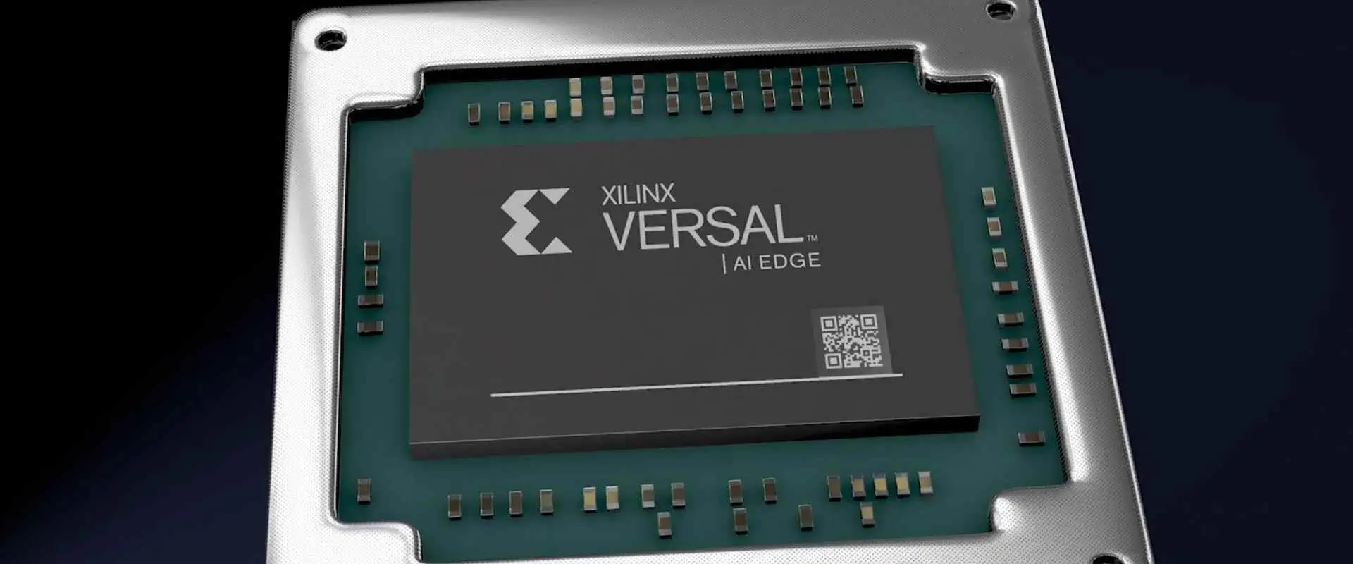
1. Spartan UltraScale+ FPGA

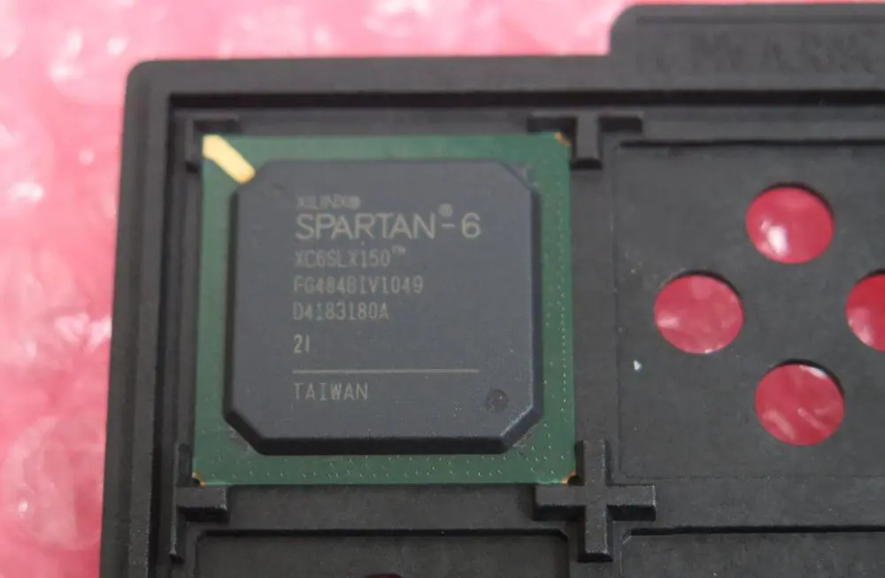
The Spartan UltraScale+ family is Xilinx’s cost-optimized FPGA solution, designed for high-volume applications that require performance and power efficiency.

Key features of Spartan UltraScale+ FPGAs:

  • Optimized for cost-sensitive markets
  • Built on 16nm FinFET+ process technology
  • Offers excellent performance-per-watt
  • Suitable for applications like industrial IoT, motor control, and entry-level video processing

2. Artix UltraScale+ FPGA

Artix UltraScale+ FPGAs provide a balance of high performance and low power consumption, making them ideal for applications that require compact form factors and energy efficiency.

Key features of Artix UltraScale+ FPGAs:

  • Built on 16nm FinFET+ process technology
  • Offers up to 64 GTH transceivers with speeds up to 16.3 Gb/s
  • Supports PCIe Gen3 and Gen4
  • Ideal for applications like software-defined radio, machine vision, and medical imaging

3. Kintex UltraScale+ FPGA

Xilinx Kintex fpga
Xilinx Kintex fpga

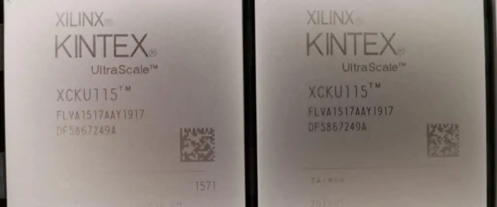
The Kintex UltraScale+ family is designed for applications that demand high performance and bandwidth while maintaining a balance with power efficiency.

Key features of Kintex UltraScale+ FPGAs:

  • Built on 16nm FinFET+ process technology
  • Offers up to 64 GTY transceivers with speeds up to 32.75 Gb/s
  • Supports PCIe Gen3 and Gen4
  • Suitable for applications like 5G wireless, data center acceleration, and high-performance computing

4. Virtex UltraScale+ FPGA

Virtex UltraScale+ FPGAs represent Xilinx’s highest-performance FPGA family, designed for the most demanding applications that require maximum throughput and processing power.

Key features of Virtex UltraScale+ FPGAs:

  • Built on 16nm FinFET+ process technology
  • Offers up to 128 GTY transceivers with speeds up to 32.75 Gb/s
  • Supports PCIe Gen3, Gen4, and Gen5
  • Ideal for applications like AI/ML acceleration, high-performance computing, and aerospace & defense

5. Zynq UltraScale+ MPSoC

Xilinx Zynq fpga
Xilinx Zynq fpga

The Zynq UltraScale+ MultiProcessor System-on-Chip (MPSoC) family combines the flexibility of FPGAs with the power of embedded processors, creating a versatile platform for a wide range of applications.

Key features of Zynq UltraScale+ MPSoCs:

  • Integrates Arm Cortex-A53 application processors and Cortex-R5 real-time processors
  • Includes Mali-400 MP2 GPU for graphics acceleration
  • Built on 16nm FinFET+ process technology
  • Suitable for applications like autonomous driving, industrial automation, and embedded vision

Read more about:

Grades of Xilinx FPGA

Xilinx offers FPGAs in various grades to meet the specific requirements of different industries and applications. These grades ensure that the FPGAs can operate reliably in diverse environments, from consumer electronics to harsh industrial settings and even space applications.

1. Automotive Grade FPGA

Automotive grade FPGAs are designed to meet the rigorous standards of the automotive industry, including extended temperature ranges, high reliability, and compliance with automotive safety standards.

(1) Artix-7 XA

The Artix-7 XA family offers a cost-effective solution for automotive applications that require high performance and low power consumption.

Key features of Artix-7 XA FPGAs:

  • AEC-Q100 qualified
  • Operating temperature range of -40ยฐC to +125ยฐC
  • Ideal for advanced driver assistance systems (ADAS) and infotainment systems

(2) Artix UltraScale+ XA

Artix UltraScale+ XA FPGAs provide higher performance and integration for automotive applications, built on the advanced 16nm process technology.

Key features of Artix UltraScale+ XA FPGAs:

  • AEC-Q100 qualified
  • Operating temperature range of -40ยฐC to +125ยฐC
  • Suitable for autonomous driving and advanced in-vehicle networking

(3) Spartan-7 XA

xilinx-spartan-7-fpga-1

The Spartan-7 XA family offers a cost-optimized solution for automotive applications that require modest performance and low power consumption.

Key features of Spartan-7 XA FPGAs:

  • AEC-Q100 qualified
  • Operating temperature range of -40ยฐC to +125ยฐC
  • Ideal for automotive body electronics and entry-level ADAS applications

2. Defense Grade FPGA

Defense grade FPGAs are designed to meet the stringent requirements of military and aerospace applications, including extended temperature ranges, radiation tolerance, and long-term reliability.

(1) Artix-7 XQ

Artix-7 XQ FPGAs offer a balance of performance and power efficiency for defense and aerospace applications.

Key features of Artix-7 XQ FPGAs:

  • MIL-STD-883 compliant
  • Extended temperature range of -55ยฐC to +125ยฐC
  • Suitable for software-defined radio and electronic warfare applications

(2) Kintex-7 XQ

Kintex-7 XQ FPGAs provide higher performance and capacity for defense applications that require increased processing power.

Key features of Kintex-7 XQ FPGAs:

  • MIL-STD-883 compliant
  • Extended temperature range of -55ยฐC to +125ยฐC
  • Ideal for radar systems and high-performance signal processing

(3) Kintex UltraScale+ XQ

Kintex UltraScale+ XQ FPGAs offer advanced performance and integration for defense applications, built on the 16nm process technology.

Key features of Kintex UltraScale+ XQ FPGAs:

  • MIL-STD-883 compliant
  • Extended temperature range of -55ยฐC to +125ยฐC
  • Suitable for advanced radar systems and high-bandwidth communications

(4) Virtex-7 XQ

Virtex-7 XQ FPGAs provide the highest performance and capacity in the 7 Series defense-grade lineup.

Key features of Virtex-7 XQ FPGAs:

  • MIL-STD-883 compliant
  • Extended temperature range of -55ยฐC to +125ยฐC
  • Ideal for complex signal processing and cryptography applications

(5) Virtex UltraScale+ XQ

Virtex UltraScale+ XQ FPGAs represent the pinnacle of defense-grade FPGA performance, offering unparalleled processing power and integration.

Key features of Virtex UltraScale+ XQ FPGAs:

  • MIL-STD-883 compliant
  • Extended temperature range of -55ยฐC to +125ยฐC
  • Suitable for advanced electronic warfare and AI-enabled defense systems

3. Space Grade

Space grade FPGAs are designed to operate in the harsh environment of space, offering radiation tolerance and reliability for satellite and space exploration applications.

(1) Kintex UltraScale XQR

The Kintex UltraScale XQR family provides high-performance, radiation-tolerant FPGAs for space applications.

Key features of Kintex UltraScale XQR FPGAs:

  • Radiation-tolerant design
  • Total Ionizing Dose (TID) tolerance of up to 100 krad(Si)
  • Single Event Upset (SEU) mitigation techniques
  • Suitable for satellite communications, Earth observation, and space exploration missions

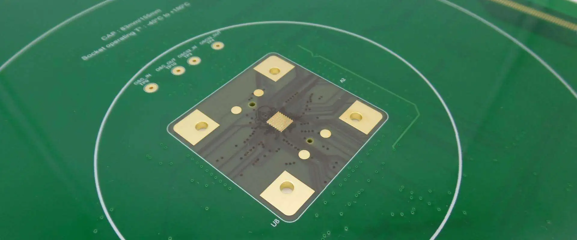
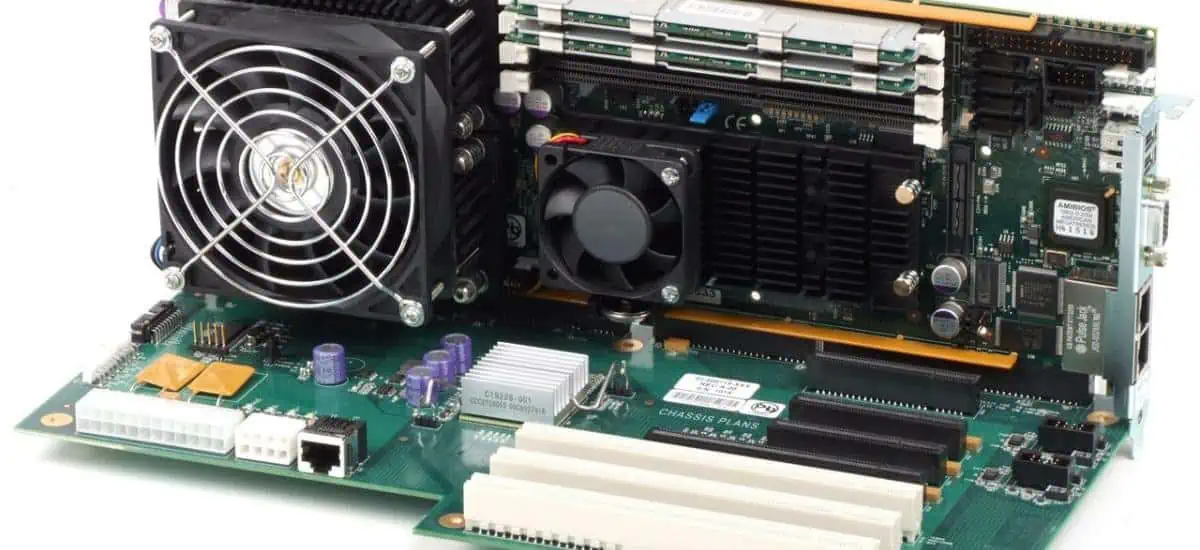
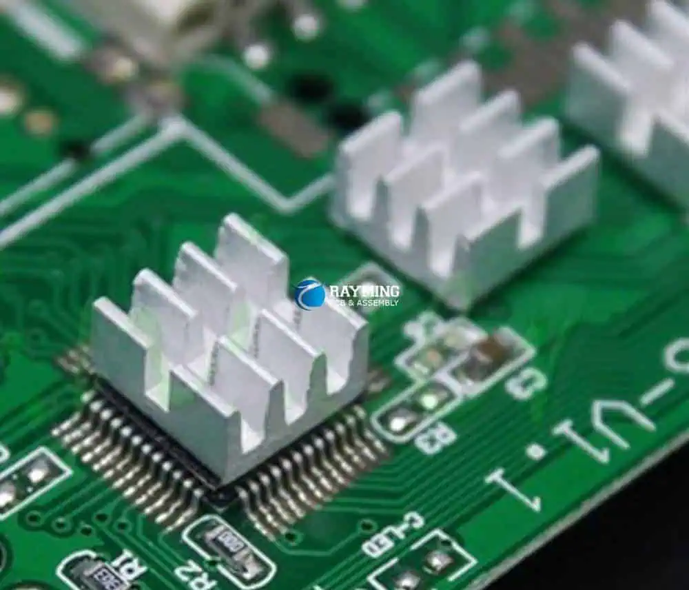
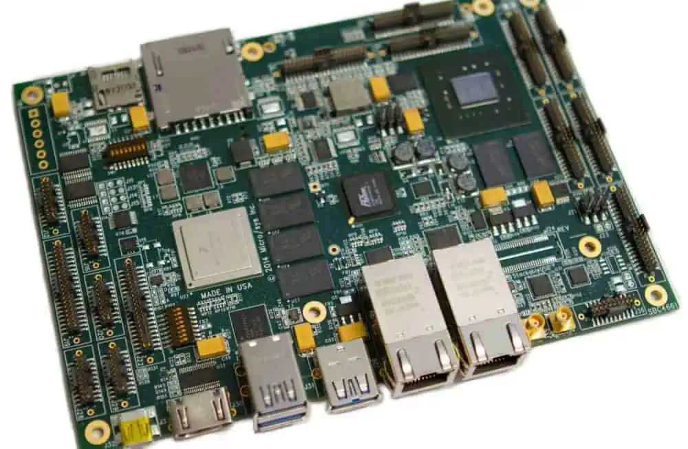
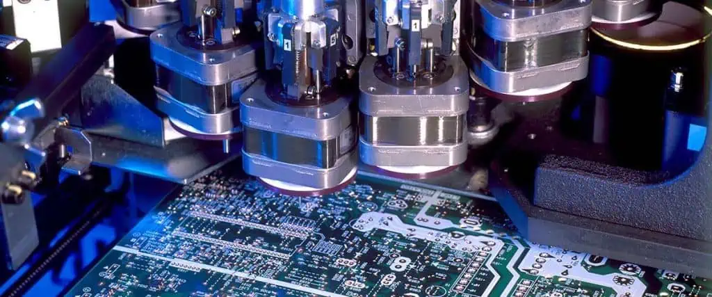
Xilinx FPGA Development Boards

Xilinx offers a wide range of development boards to help engineers and researchers prototype and test their designs using Xilinx FPGAs. These boards provide a convenient platform for exploring the capabilities of Xilinx FPGAs and developing applications across various domains.

Some popular Xilinx FPGA development boards include:

  1. Alveo Accelerator Cards: Designed for data center acceleration, these cards feature high-performance Xilinx UltraScale+ FPGAs.
  2. Zynq UltraScale+ MPSoC ZCU104 Evaluation Kit: A versatile platform for evaluating Zynq UltraScale+ MPSoCs, ideal for embedded vision and industrial IoT applications.
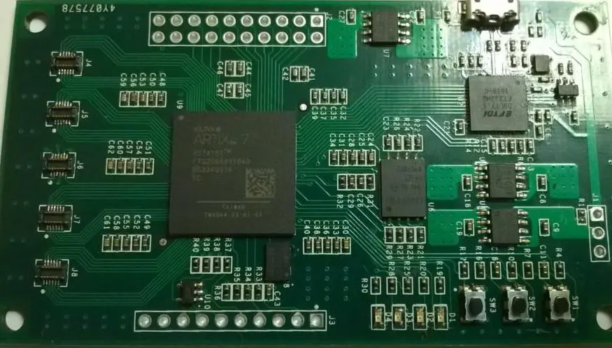
  3. Artix-7 FPGA Development Board: A cost-effective board for prototyping designs using Artix-7 FPGAs, suitable for various applications.
  4. Kintex UltraScale FPGA KCU116 Evaluation Kit: A high-performance development platform for exploring Kintex UltraScale FPGAs, ideal for communications and signal processing applications.
  5. Virtex UltraScale+ VCU118 Evaluation Kit: A cutting-edge development board featuring Virtex UltraScale+ FPGAs, designed for high-end applications and research.

These development boards come with comprehensive software support, including Xilinx’s Vivado Design Suite and Vitis unified software platform, enabling developers to quickly prototype and optimize their FPGA designs.

Cost of Xilinx FPGAs

Xilinx FPGA distributor

The cost of Xilinx FPGAs varies widely depending on the product family, performance capabilities, and volume of purchase. Here’s a general overview of the cost ranges for different Xilinx FPGA families:

  1. Spartan Series: 10โˆ’10โˆ’100+
    • Lowest cost option, suitable for high-volume applications
    • Price varies based on logic capacity and features
  2. Artix Series: 50โˆ’50โˆ’500+
    • Mid-range option balancing cost and performance
    • Price depends on logic capacity, transceiver count, and other features
  3. Kintex Series: 500โˆ’500โˆ’5,000+
    • Higher-performance option with increased logic capacity and features
    • Price varies significantly based on specific model and capabilities
  4. Virtex Series: 2,000โˆ’2,000โˆ’20,000+
    • High-end FPGAs with maximum performance and features
    • Pricing reflects the advanced capabilities and large logic capacities
  5. Zynq UltraScale+ MPSoCs: 500โˆ’500โˆ’10,000+
    • Pricing depends on the specific model, processor cores, and FPGA resources
    • Higher-end models with more powerful processors and larger FPGA fabric command premium prices

It’s important to note that these price ranges are approximate and can vary based on factors such as:

  • Volume of purchase: Bulk orders often receive discounts
  • Distribution channel: Prices may differ between authorized distributors
  • Specific model and features: Within each family, prices vary based on exact specifications
  • Market conditions: Prices can fluctuate due to supply and demand dynamics

For precise pricing information, it’s best to contact Xilinx or authorized distributors directly. Additionally, consider the total cost of ownership, including development tools, support, and power consumption, when evaluating FPGA solutions for your project.

Xilinx FPGA Application Markets

Xilinx FPGAs find applications across a wide range of industries and markets, thanks to their flexibility, performance, and ability to adapt to evolving standards. Here are some key application markets for Xilinx FPGAs:

1. Telecommunications and Networking

Xilinx FPGAs play a crucial role in the telecommunications industry, particularly in the development and deployment of 5G networks. They are used in:

  • 5G base stations and remote radio heads
  • Network function virtualization (NFV)
  • Software-defined networking (SDN)
  • High-speed optical transport networks

2. Data Centers and Cloud Computing

In the rapidly evolving world of data centers, Xilinx FPGAs provide acceleration for various workloads:

  • AI and machine learning inference
  • Database acceleration
  • Video transcoding and streaming
  • Network acceleration and security

3. Automotive

The automotive industry leverages Xilinx FPGAs for advanced driver assistance systems (ADAS) and autonomous vehicles:

  • Sensor fusion and processing
  • Computer vision for object detection and recognition
  • In-vehicle networking and infotainment systems
  • Functional safety systems

4. Aerospace and Defense

Xilinx’s defense-grade FPGAs are widely used in aerospace and defense applications:

  • Radar and electronic warfare systems
  • Satellite communications
  • Secure communications and cryptography
  • Avionics and flight control systems

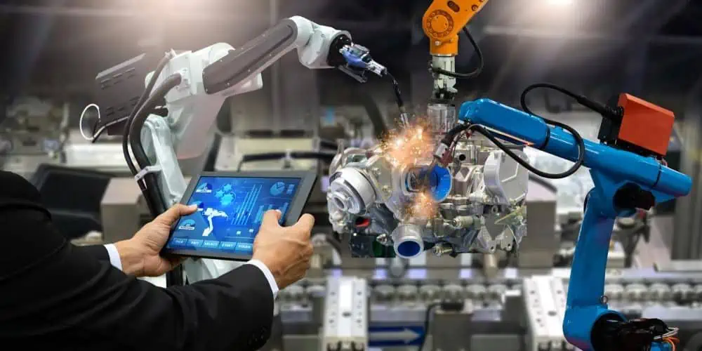
5. Industrial Automation and IoT

In the industrial sector, Xilinx FPGAs enable smart manufacturing and Industry 4.0 initiatives:

  • Industrial robotics and motion control
  • Machine vision and quality inspection
  • Industrial IoT gateways and edge computing
  • Predictive maintenance systems

6. Healthcare and Medical Devices

Xilinx FPGAs contribute to advancements in medical technology:

  • Medical imaging systems (MRI, CT, ultrasound)
  • Real-time patient monitoring devices
  • DNA sequencing and bioinformatics
  • Surgical robots and assistance systems

7. Broadcast and Pro A/V

The media and entertainment industry relies on Xilinx FPGAs for:

  • 4K/8K video processing and encoding
  • High-definition video switching and routing
  • Real-time graphics rendering
  • Virtual and augmented reality systems

8. Consumer Electronics

While not as prevalent as in other markets, Xilinx FPGAs find their way into high-end consumer products:

  • High-performance gaming systems
  • Digital cameras and camcorders
  • Smart home devices and IoT hubs
  • Audio processing equipment

9. Scientific Research and High-Performance Computing

Xilinx FPGAs are valuable tools in scientific research and high-performance computing:

  • Particle physics experiments (e.g., at CERN)
  • Climate modeling and weather forecasting
  • Financial modeling and high-frequency trading
  • Quantum computing research and development

The versatility of Xilinx FPGAs allows them to address the unique challenges of each of these markets, providing customizable, high-performance solutions that can adapt to changing requirements and standards.

Conclusion

Xilinx FPGAs represent a powerful and versatile technology that continues to shape the landscape of digital design across numerous industries. From the cost-effective Spartan series to the high-performance Virtex UltraScale+ family, Xilinx offers a comprehensive range of FPGA solutions to meet diverse application needs.

The various grades of Xilinx FPGAs, including automotive, defense, and space-grade options, ensure that these flexible devices can operate reliably in even the most demanding environments. With development boards and robust software tools, Xilinx provides a complete ecosystem for engineers and researchers to innovate and bring their ideas to life.

While the cost of Xilinx FPGAs can vary significantly depending on the specific model and features, the total value proposition extends beyond the initial price. The flexibility, performance, and long-term adaptability of FPGAs often result in reduced overall system costs and faster time-to-market for many applications.

The wide range of application markets for Xilinx FPGAs demonstrates their versatility and importance in driving technological innovation. From telecommunications and data centers to automotive and healthcare, Xilinx FPGAs are at the forefront of enabling new capabilities and improved performance across industries.

As we look to the future, the role of FPGAs is likely to become even more critical. With the increasing demand for AI and machine learning at the edge, the need for customizable, high-performance computing solutions will only grow. Xilinx, now part of AMD, is well-positioned to continue driving innovation in the FPGA space, offering solutions that meet the evolving needs of developers and industries worldwide.

What is Near Field Communication (NFC) ?

Near Field Communication or NFC refers to a short-range wireless connectivity technology that enables simple and secure communication between devices that are in close proximity. NFC offers capabilities like contactless transactions, data exchange, device pairing and proximity-based interactions.

In this comprehensive guide, we will cover the fundamentals of NFC technology, how it works, protocols, standards, device integration, security considerations, use cases and its evolution.

Introduction to NFC

NFC or Near Field Communication is a standards-based wireless connectivity technology that allows devices within a short range to exchange information securely.

Some key aspects of NFC:

  • Operates at 13.56 MHz frequency based on RFID standards
  • Offers data speeds from 106 kbps to 424 kbps
  • Supports communication distances up to 10 cm
  • Enables intuitive “tap” based interactions between devices
  • Secure two-way communication between endpoints
  • Low power consumption for battery-powered devices

NFC enables compelling use cases like:

  • Contactless transactions via payment cards and terminals
  • Quick pairing between smartphones, peripherals and IoT devices
  • Sharing contacts, media files, web links etc through a simple tap
  • Fetching information from smart posters, tags and stickers via proximity
  • Automated actions and access control by bringing devices close together

NFC complements broader connectivity technologies like WiFi and Bluetooth by adding a short-range, low-power interaction model. Next, we will take a technical look under the hood at how NFC systems function.

How NFC Wireless Communication Works

NFC is based on RFID or Radio Frequency IDentification standards and operates in the globally available 13.56 MHz ISM band. It leverages electromagnetic induction between two loop antennas located within each other’s near field for communication.

The major components involved are:

NFC Reader/Writer – Actively generates an RF field and can read from or write data to compatible devices. Examples are payment terminals, smartphone NFC adapters.

NFC Tag – Passive tag that modulates data to the reader by detuning the RF field. Tags contain data and an NFC antenna.

NFC Peer-to-Peer – Two NFC-capable devices can exchange data in peer-to-peer mode.

NFC Card Emulation – Payment cards simulate an NFC tag to transmit card data to readers.

The basic NFC communication flow is:

  1. The reader/initiator generates an unmodulated 13.56 MHz RF carrier field.
  2. The tag or peer device draws power from the RF field and communicates by load modulation.
  3. Data is transmitted between the endpoints using modulation like ASK or PSK encoding schemes.
  4. Bit rates of 106, 212 or 424 Kbps are supported for communication.

This near field working range limits NFC connections typically to around 10 cm or less. NFC transmissions are also inherently secure since the short range limits eavesdropping/interception risks. Next, we look at the protocols and data exchange mechanisms supported by NFC.

NFC Protocols and Data Exchange

NFC defines standardized mechanisms for communication session initialization and data exchange between two devices. The core protocols are:

NFC Logical Link Control Protocol (LLCP)

LLCP allows two NFC-enabled peer devices to communicate in both directions. LLCP sets up the logical data communication channel and provides a reliable, orderly data exchange between the peer devices.

Key capabilities offered by LLCP include:

  • Service discovery – discover available services on the peer
  • Symmetry – both devices can send and receive

-Segmentation and reassembly – large packets are split and recombined

  • Multiplexing – communicate over multiple data links
  • Error handling – ensure data integrity
  • Flow control – manage transmission speed

LLCP is required for Android Beam file transfer and NFC based WiFi setup between Android devices. It can transport any application protocol.

NFC Data Exchange Format (NDEF)

NDEF defines a common data format for NFC messages transmitted between devices. The NDEF specification determines:

  • Message encapsulation – how payload is packaged
  • Record typing – assign record types like text, URI, binary etc.

-security handling

  • extensibility to add new record types

NDEF ensures interoperability between sender and receiver devices by establishing a standard data representation. This allows easy peer-to-peer exchange of things like contacts, web URLs, configuration parameters etc. simply by tapping devices together.

In card emulation mode, payment or transit cards also use NDEF to encapsulate data transmitted to the reader.

NFC Record Type Definitions (RTD)

RTDs provide specifications for various standardized record types like smart posters, text, URIs, Bluetooth handover etc. This allows common handling of these record types across devices.

For example, the Smart Poster RTD allows an NFC phone to consistently identify and interpret data from any compliant smart poster tag. RTDs ensure interoperability across the ecosystem.

Together, these protocols provide the foundation for reliable, interoperable data exchange between NFC devices.

NFC Operating Modes

NFC endpoints can communicate using several different operating modes:

Reader/Writer Mode

In this mode, the NFC device reads data from or writes data into passive NFC tags and stickers. This allows tagging real world objects and embedding information.

Use cases like asset tracking, smart packaging, interactive signage and contactless payments leverage reader/writer mode.

Card Emulation Mode

Here the NFC device like a smartphone emulates an NFC tag to another reading device like a payment terminal. This allows payments, transit ticketing and access control using the phone instead of a card.

The phone loads payment, ticketing, access control credentials into its secure element and presents it just like a contactless card when in proximity.

Peer-to-Peer (P2P) Mode

In P2P mode, two NFC-capable devices can exchange data like contacts, media files, web links etc. Android Beam leverages P2P mode. WiFi handoff also uses NFC P2P to exchange credentials.

P2P mode enables quick tapping to pair and share data across NFC devices.

By supporting these modes of communication, NFC delivers a diverse set of applications for consumers and enterprises, which we will cover later.

NFC Frequency Bands and Data Rates

NFC systems operate in the globally available, license-free 13.56 MHz ISM band. This frequency is leveraged since most countries allow free usage of 13.56 MHz band for industrial, scientific and medical purposes.

Within this ISM band, NFC implementations can take one of three possible carrier frequency choices:

  • 13.553 to 13.567 MHz – Center frequency 13.56 MHz
  • 13.56605 to 13.56795 MHz – Center frequency 13.56 MHz
  • 13.824 to 14.224 MHz – Center frequency 13.56 MHz

NFC antennas and coils are tuned for high efficiency at the center frequencies. The three sub-band options within ISM allow regional flexibility.

In terms of link data rate, NFC supports:

  • 106 kbit/s – Based on ISO/IEC 18092 standard
  • 212 kbit/s – For passive communication mode
  • 424 kbit/s – High data rate, active communication mode

Higher rates allow exchange of more data when devices are tapped together. 424 kbps is fast enough for quick small file or web page sharing between phones or computers using NFC.

NFC Standards

NFC technology has been standardized in multiple stages by standards bodies like:

ISO – International Organization for Standardization

IEC – International Electrotechnical Commission

ETSI – European Telecommunications Standards Institute

ECMA – European association for standardizing ICT and consumer electronics

NFC Forum – Standards body managing NFC specifications

Here is an evolution of key NFC standards:

  • ISO/IEC 18092 – Published 2004, defined modulation schemes and data transport
  • ISO/IEC 21481 – Published 2005, defined NFC interface and protocol
  • ECMA-340 – Published 2006, defined NFC peer-to-peer standards
  • ECMA-352 – Published 2008, defined NDEF data format
  • ISO/IEC 22536 – Published 2011, harmonized former standards
  • NFC Forum Specifications – Define implementation, use cases, testing

These standards ensure interoperability between NFC devices from different manufacturers. Let’s next look at the typical architecture for NFC controller chips and antennas.

NFC Hardware Architecture

The key hardware needed on a device for NFC functionality includes:

NFC Controller

This chip manages the wireless connectivity, communication protocols and data exchange with other NFC endpoints. It modulates and demodulates transmitted data.

Most NFC controllers integrate a secure element hardware block that stores payment or other sensitive credentials in a tamper-resistant manner.

Some example NFC controllers are:

  • NXP PN544 – Popular NFC controller used in many smartphones
  • NXP PN548 – High performance controller with integrated secure element
  • ST ST21NFC – NFC controller chip by STMicroelectronics

NFC Antenna

The NFC antenna is tuned to the 13.56 MHz frequency and allows the device to transmit and receive NFC signals. It is designed to offer good coupling with other NFC antennas that come in proximity.

NFC antennas typically consist of a copper coil etched onto a printed circuit board assembly. Multiple coil turns are used with 1nH typical inductance. Matching is done with capacitors.

Host Processor Interface

The NFC controller communicates with the main application processor of the device over standard interfaces like SPI, I2C, UART, USB. Software stacks use these interfaces.

NFC Power Management

Switches, regulators and amplifiers provide stable power supply to the NFC chips derived from the system battery voltage.

The controller, antenna and associated interfaces come together into an integrated NFC hardware module packaged as a single chip or PCB assembly for integration into the device.

Software Architecture

Here are some key components of the NFC software stack:

Host API – Allows applications to leverage and control NFC hardware capabilities

NFC Middleware – Manages interaction between applications, secure elements and hardware

Device Firmware – Low level firmware like RF analog control and digital protocol stack

Upper Layer Protocols – Software for protocols like LLCP, P2P, SNEP

Payment/Access Control Apps – Software for emulating transit cards, access cards

Peer-to-Peer Apps – Program logic for use cases like file sharing

Tag Reading Apps – Code to read, write and emulate NFC tags

On Android, the NFC software stack is implemented via Android’s NFC HAL (Hardware Abstraction Layer) and utilizes the NFC Forum Logical Link Control Protocol (LLCP) for peer-to-peer communication.

Apple implements similar software architecture within its CoreNFC frameworks introduced in iOS 11.

The firmware and software together orchestrate NFC operations, protocol handling, secure data exchange and use case management.

NFC Integration Into Devices

Here are some guidelines and considerations when integrating NFC hardware into a device:

  • Select NFC controller and antenna that supports target read range, power budgets
  • Ensure NFC module placement allows space for antenna and minimizes interference
  • Route signals from controller to host processor using robust interfaces like I2C
  • Provide sufficient decoupling and power supply stability to NFC module
  • Utilize shielding, ferrite sheets to limit interference from other subsystems
  • Over-the-air testing to validate read range, data speeds, accuracy
  • Test NFC performance in final device enclosure, with batteries, displays
  • Validation testing with representative NFC tags and reader devices

With careful integration, antenna tuning and testing, optimal NFC performance can be delivered within the device.

NFC Security Considerations

NFC offers simplified connectivity between devices, however it is important to keep security in mind:

Data Exchange

  • NFC’s short range limits potential for remote eavesdropping and man-in-the-middle attacks.
  • Encryption can be implemented for NDEF and application level data security.

Device Pairing

  • Visually confirm identity of the peer device being paired for consent.

Tags and Stickers

  • Avoid unexpectedly downloading or opening unverified content from unknown smart tags.

Relay Attacks

  • Guard against Attempts to relay or extend unauthorized NFC scans beyond immediate vicinity.

Transaction Verification

  • Double check transaction details on device screen before approving contactless payments.

Secure Element

  • Use hardware backed secure element for storage of payment credentials and keys.

By following device best practices and user awareness, NFC can be implemented securely across applications.

Applications and Use Cases

nfc manufacturer

Some major applications leveraging NFC technology include:

1. Contactless Payments

NFC enables card emulation mode on phones allowing users to tap to pay at POS terminals – fast, convenient and secure.

Contactless transactions under a certain value threshold often do not even need additional authentication. Major payment networks like Visa, Mastercard, American Express and Discover support NFC payments.

2. Transit Ticketing

NFC offers a convenient contactless ticketing solution for public transport. Riders simply tap their phone or ticket on bus validators for seamless access. Solution minimizes ticket lines.

Transit agencies save on issuing and managing disposable cards. Most major transport systems globally support NFC ticketing.

3. Access Control

NFC access cards for secure door entry can be replaced with an NFC enabled phone. Employees just tap their phone to enter secured office doors, data centers etc.

Easy issuance, revocation of digital credentials on the phone compared to plastic cards.

4. Device Pairing

Android Beam, Apple Wallet leverage NFC’s peer-to-peer mode to quickly transfer data like contacts, web URLs, documents etc. by tapping devices.

Tap can also be used to connect or configure peripherals like headphones, printers and speakers.

5. Information Sharing

Smart posters, tags and stickers with embedded NFC tags allow businesses to share information with a simple tap of the phone.

Can be used for interactive advertising, sharing menus, product info, schedules, in-store navigation etc.

6. Gaming Interactions

NFC enables interactive board games, playing cards and collectible toys by adding a digital dimension via the phone.

7. Automotive Use Cases

NFC can enable vehicle features like keyless entry and start, personalized dashboard profiles, garage door opening, parking payments etc.

8. Industrial Applications

NFC is also gaining adoption in industries to track assets, for equipment maintenance, factory automation, lab instrument management and other uses leveraging proximity based interactions and data exchange.

These examples illustrate the versatile applicability of NFC technology across consumer and enterprise segments.

The Future of NFC Technology

NFC has become firmly established over the past decade as a ubiquitous proximity wireless communication technology. Here are some trends shaping NFC’s future roadmap:

Increased Adoption in Smartphones – A growing number of smartphones now incorporate NFC allowing large addressable user base for applications.

IoT Connectivity – NFC offers easy pairing between IoT devices and homeowners’ smartphones to set up and manage appliances, smart home systems.

Advancing NFC Standards – Standards like NFC-V for vehicle integration and NFC-F for high data rate are emerging for new use cases.

NFC for Digital Key Sharing – Smart door locks and key cabinets are leveraging NFC to securely share digital keys using people’s phones.

Stronger Security – Advancing secure element, tokenization and biometric authentication technologies reinforce security of NFC payments and access control.

New Form Factors – Embedding NFC into more wearables, hearables, tablets and compute devices expands capabilities.

Innovation in Antennas – NFC performance is improving through integration, advanced antenna topologies like using magnetic induction.

NFC will continue evolving alongside smartphones and IoT endpoints to deliver more intuitive, convenient and secure interactions between people, devices and environments.

Conclusion

nfc-stickers

This brings us to the end of this comprehensive guide to NFC technology. We discussed how NFC systems function using inductive coupling, the communication mechanisms and protocols, integration considerations, security, applications across segments and the role of advancing standards.

NFC delivers a compelling blend of convenience, versatility and security to enable natural interactions using mobile devices. With applications from payments, transportation to interactive gaming and industrial automation, NFC adoption will continue growing as more smart objects populate our environment.

FAQs (Frequently Asked Questions)

How is NFC different from other wireless tech like RFID, Bluetooth and WiFi?

NFC offers very short range (touch-based), operates at 13.56MHz with low power consumption ideal for battery devices, and supports peer-to-peer mode.

What is the typical read range offered by NFC?

Practical NFC working distance is typically under 10cm. The proximity allows intuitive usage while providing inherent security against remote attacks.

Does NFC require pairing between devices before working?

NFC does not require traditional pairing and can securely exchange data between devices with just a tap without prior setup.

What data rates does NFC support?

NFC offers data rates ranging from 106 kbps to 424 kbps depending on implementation which is adequate for small data transactions.

What are some examples of NFC enabled devices?

Most modern smartphones, tablets, wearables, wireless headsets, smart home devices, retail terminals incorporate NFC.

What is an Arduino:Types, Projects and Applications ?

Introduction to Arduino

Arduino is an open-source electronics platform based on easy-to-use hardware and software. Arduinos make it simple for hobbyists and professionals to develop interactive electronics projects.

The key aspects of Arduino are:

  • Open-source – Hardware and software are open for anyone to use and modify.
  • Easy to use – The Arduino IDE and wiring interfaces abstract away complexity for beginners.
  • Flexible – Arduino boards can interface with a wide range of sensors, displays, motors, and other electronic components.
  • Inexpensive – The affordable boards make Arduino accessible for makers, students, and developers.
  • Cross-platform – Arduino software runs on Windows, Mac, Linux and cloud platforms.

Arduino has become the most popular open-source electronics platform, allowing millions of users to create interactive devices. Let’s examine Arduino boards, software, projects and applications in more detail.

Arduino Board Types

There are many types of Arduino boards available to meet different application needs. Here are some of the most common official Arduino board families:

Arduino Uno

The Arduino Uno is the classic entry-level Arduino board. It provides everything needed to start developing simple Arduino projects. Key features include:

  • Microcontroller: ATmega328P
  • Operating Voltage: 5V
  • I/O Pins: 14 Digital, 6 Analog
  • Flash Memory: 32 KB
  • Clock Speed: 16 MHz

With abundant tutorials and examples, the beginner-friendly Uno is the ideal starting point into Arduino.

Arduino Mega

The Arduino Mega2560 upgrades to a more powerful microcontroller chip and extensive I/O capabilities:

  • Microcontroller: ATmega2560
  • Operating Voltage: 5V
  • Digital I/O Pins: 54
  • Analog Input Pins: 16
  • Flash Memory: 256 KB
  • Clock Speed: 16 MHz

The Mega2560 is well suited for more complex projects requiring additional memory, processing power, and I/O lines.

Arduino Nano

The Arduino Nano packs the power of the Uno into a compact surface mount board:

  • Microcontroller: ATmega328P
  • Operating Voltage: 5V
  • Digital I/O Pins: 14
  • Analog Input Pins: 8
  • Flash Memory: 32 KB
  • Clock Speed: 16 MHz

With its small size, breadboard-friendly design, and abundance of I/O, the Nano is ideal for dense circuit prototyping.

Arduino Leonardo

The Arduino Leonardo differs by employing an ATmega32U4 microcontroller with built-in USB communication:

  • Microcontroller: ATmega32U4
  • Operating Voltage: 5V
  • Digital I/O Pins: 20
  • Analog Input Pins: 12
  • Flash Memory: 32 KB
  • Clock Speed: 16 MHz

The Leonardo can appear as a standard USB mouse or keyboard, facilitating HID projects.

Arduino MKR Family

The MKR boards offer compact, low power WiFi and cellular connectivity:

  • Microcontroller: ATSAMD21 Cortex-M0+
  • Operating Voltage: 3.3V
  • Digital I/O Pins: 8-12
  • Analog Input Pins: 6-8
  • Flash Memory: 256-512 KB
  • Connectivity: WiFi, GSM, LoRa

Choose an MKR board for IoT and wireless communication projects.

There are many other specialty Arduino boards like the MKR Vidor 4000 FPGA, ESplora with built-in sensors, and Portenta H7 with dual cores. This highlights the diversity of Arduino hardware.

Arduino Software

A key aspect of Arduino is its easy-to-use open source software. The Arduino IDE provides everything needed to program the boards in simple C/C++ based scripts.

The Arduino software includes:

  • Text editor for writing code
  • Compiler to build sketches
  • Uploader for installing sketches to an Arduino
  • Serially monitor Arduino communications
  • Libraries and examples to simplify coding

The flow involves:

  1. Writing a sketch using Arduino functions and libraries
  2. Compiling the sketch into executable code
  3. Uploading the hex file to the Arduino’s microcontroller

No advanced coding or hardware configuration is required. Arduino provides a seamless platform for programming interactive electronics projects.

Arduino Projects

Arduino’s versatility enables beginners to experts to create a huge variety of projects. Some examples include:

Basic Input/Output

  • LED light patterns
  • Reading switches and buttons
  • Driving motors, buzzers, and relays
  • Displaying text and shapes on LCDs

These simple but engaging projects teach Arduino I/O control.

Sensors

  • Motion detection with PIR sensors
  • Measuring temperature, humidity and gases
  • Detecting light levels with photoresistors
  • Capturing sound with a microphone
  • Ultrasonic and infrared distance ranging

Arduino is commonly used for sensor interfacing and data acquisition.

Robotics

  • Autonomous robot cars sensing the environment
  • Robotic arms with servos
  • Self-balancing robots
  • Swarm robots
  • Hexapod walking robots

Arduino provides an accessible brain for powering robots.

IoT and Wireless

  • Home automation with Bluetooth/WiFi
  • Weather stations sending data
  • Location trackers with GPS
  • Transmitting sensor telemetry
  • Smart agriculture monitoring

Arduino enables a range of wireless IoT edge devices.

Wearables

  • Fitness and health trackers
  • Smart watches
  • Virtual reality/augmented reality gear
  • Fashion tech
  • Assistive technology

Arduino can create interactive wearable electronics projects.

The applications are endless – if you can think of an electronics project, an Arduino can probably bring it to life!

Arduino Project Design Process

A structured development process helps ensure success as you design your Arduino project:

1. Define Objectives

  • What are the goals of your project? Desired functionality?

2. Flowchart Concepts

  • Diagram the logical flow and capabilities.

3. Select Components

  • Choose which Arduino board, sensors, displays and other components are needed.

4. Prototype the Circuit

  • Build the circuit on a breadboard and test functionality.

5. Write the Code

  • Program the Arduino to operate your circuit and application.

6. Troubleshoot and Refine

  • Fix issues, improve performance through an iterative process.

7. Construct Permanent Project

  • Solder your circuit and integrate into an enclosure or finished project.

This systematic approach will produce robust, high-quality Arduino projects.

Arduino Project Enclosure

arduino FPGA PCBA
arduino FPGA PCBA

For building permanent Arduino devices beyond a breadboard prototype, you need to integrate your project into an enclosure. Some options include:

  • Plastic boxes – Common for small projects, provides protection.
  • 3D printed cases – Design fully customized housings.
  • Laser cut enclosures – Stylish acrylic or wood cases.
  • Aluminum extrusion frames – An open modular support skeleton.
  • Machined enclosures – For metal housings with complex features.
  • Textile crafts – Knitted, sewn, or woven integrateion.
  • Portable batteries – Self-contained power for mobile projects.

Choose enclosures suited to your project’s mechanical, aesthetic, and functional requirements.

Applications of Arduino

Due to its versatility, there are limitless applications for Arduino across industries:

Education

Arduino provides an excellent hands-on platform for learning about electronics and programming in engineering, computer science, robotics, and physics courses. Arduino curriculum brings theoretical concepts to life.

Industrial Automation

For automation applications, Arduino can monitor sensors, valves, motors, process variables, and manufacturing lines. Arduino offers a low-cost programmable control platform.

Science Experiments

Arduino is valued by scientists for data acquisition and experimental controls. Arduino systems can automate experiments and record results.

Home Automation

In home automation, Arduino boards can integrate appliances, lighting, climate, security, pet care, and media systems into an intelligent connected home.

Audio Effects

For musicians, Arduino enables innovative synth pedals and audio effects like delays, distortions, loopers, and specialized real-time audio processing.

Assistive Technology

For adaptive needs, Arduino can interface with switches, wheelchairs, speaking aids, alternate input devices, alarms, and environmental controls.

Internet of Things

Arduino boards form the core of many networked monitoring and control systems with wireless connectivity to the cloud.

Wearable Technology

On wearables, Arduino provides a tiny programmable computer to make clothing and accessories interactive with sensors and LEDs.

From lab instruments to interactive art, Arduino serves limitless applications where an affordable, custom microcontroller system is needed.

Arduino Alternatives

While extremely popular, Arduino has inspired many other open-source hardware platforms. Some popular alternatives include:

  • Raspberry Pi – Low-cost single board computers running Linux. More power for applications like machine learning, computer vision, and network servers.
  • ESP32 – Microcontrollers with built-in WiFi and Bluetooth. For IoT and wireless products.
  • BeagleBoards – Open-source development boards with more processing performance for advanced applications.
  • SparkFun Inventor’s Kits – Curated electronics component kits teaching technology fundamentals.
  • STM32 – ARM Cortex MCUs with extensive I/O options and networking support.
  • PICAXE – All-in-one microcontroller boards focused on education.

Each platform has unique capabilities for different use cases. Arduino remains the most beginner-friendly choice.

Conclusion

In summary, Arduino provides an accessible open-source ecosystem for interactive electronics projects. Arduino boards offer an inexpensive microcontroller foundation with easy-to-use software. This empowers makers, students, researchers, and engineers to build innovative devices for just about any application. Arduino will continue fueling the creativity of the open-source hardware community for years to come.

Frequently Asked Questions

What are the main benefits of using Arduino vs. other microcontrollers?

The main advantages are beginner-friendly hardware, simplified programming, extensive documentation and examples, and low cost boards to get started.

What are some tips for starting out with Arduino?

Start with simple circuits to learn fundamentals. Seek example projects similar to your application. Use libraries when possible. Seek help from the large Arduino community.

Which sensors are most commonly used with Arduino?

Some of the most popular sensors are ultrasonic, accelerometer, gyroscope, magnetometer, temperature, force, capacitive touch, infrared, humidity, and gas sensors.

Can Arduino be used for advanced robotics?

Yes, Arduino can perform complex control tasks with the help of add-on motor controllers and advanced sensor systems. More powerful Arduino boards provide needed performance.

What is a good next step after learning Arduino basics?

Moving to alternative microcontroller platforms like Raspberry Pi or ESP32 allows creating more advanced IoT, network, and machine learning driven systems.

Full Introduction about Fr4 Dielectric Constant

PTFE Dielectric Constant

What is the Dielectric Constant?

The dielectric constant (Dk) is a property of insulator materials that describes how readily the material can transmit an electric field. It is defined as the ratio of the permittivity of the material to the permittivity of free space. A higher dielectric constant indicates more concentration of electric flux for a given applied voltage.

For printed circuit boards, the Dk of the substrate laminate materials directly impacts key parameters like impedance, capacitance, and propagation delay which influence signal integrity, EMI control, and many other aspects of circuit performance. As such, having a solid understanding of PCB dielectric properties is important for electrical engineers.

In this comprehensive guide, weโ€™ll cover everything you need to know about the FR4 dielectric constant specifically, including its meaning, typical values, impact on circuit design, how it varies based on composition, frequency, humidity, temperature, and more. Letโ€™s get started!

What is FR4 Material?

FR4 is the generic designation for the most common type of fiberglass-reinforced epoxy laminate material used as the substrate for rigid printed circuit boards. Some key attributes of FR4 include:

  • Glass fabric base material impregnated with flame-retardant epoxy resin
  • Available in wide range of thicknesses, typically from 0.4mm to 6mm
  • Composite construction provides mechanical strength and stability
  • Low cost, widely available, and well characterized for PCB fabrication
  • Used in vast majority of rigid PCB applications across consumer and industrial electronics

The FR4 designation comes from the flame-retardant treatment incorporated in the epoxy resin system. This gives the material enhanced fire resistance properties important for safe electronics assembly.

Multiple fabricators worldwide produce FR4 material in various grades under numerous trade names. But the performance is typically comparable for most general circuit board applications.

Typical FR4 Dielectric Constant

The dielectric constant of basic FR4 laminate materials commonly falls between 3.9 and 4.8 across frequencies up to around 1 GHz. Some examples include:

  • Isola FR408 HR – 3.9 to 4.4 over 1 MHz to 10 GHz
  • Nelco N4000-13 – 4.4 at 1 MHz falling to 4.1 at 1 GHz
  • Arlon CLTE – 4.7 over 1 MHz to 1 GHz
  • Taconic TLY – 4.6 over 100 MHz to 1 GHz

So in summary, assuming a Dk of 4.2-4.4 is reasonable for baseline budgetary FR4 dielectric assumptions up to GHz frequencies.

Of course, specialized FR4 blends are available from vendors with Dk values above and below the norm to meet particular requirements. Always check manufacturer data sheets for guaranteed properties.

Impact of Dielectric Constant on PCBs

The FR4 dielectric constant directly influences key electrical parameters that must be considered during circuit board layout and optimization. Some of the major interrelated impacts include:

Impedance

For a given PCB trace width and height over the ground plane, a higher Dk allows a higher characteristic impedance to be achieved. This impedance matching is vital for signal integrity.

Capacitance

A higher Dk leads to increased parasitic capacitance between conductors as greater electric flux can be stored. This must be considered for maintaining desired frequency response.

Propagation Delay

Signals propagate more slowly in higher Dk materials, increasing delay and flight times through traces which can limit high-speed performance.

Crosstalk

Faster signal edge rates coupled with higher Dk can increase crosstalk coupling to nearby traces which may require wider spacing.

Loss Tangent

Materials with higher Dk often have higher loss tangents, contributing more signal loss due to dielectric absorption.

EMI Susceptibility

Higher Dk materials concentrate more electrical flux, increasing susceptibility to external EMI interference.

Via Performance

With higher Dk, vias exhibit increased capacitive discontinuities, negatively impacting signal transmission through layer transitions.

In summary, the FR4 Dk impacts impedance control, propagation speed, parasitic capacitance, signal loss, EMI immunity, and more. Accounting for these effects is key during circuit optimization.

FR4 Dielectric Constant Variation

Itโ€™s important to understand that the FR4 dielectric constant is not a fixed value – it can vary based on several factors:

Resin Composition

The precise epoxy resin system used in the FR4 formulation impacts the dielectric constant. Values may differ slightly between various material suppliers.

Filler Composition

Dielectric properties change based on the filler content in the epoxy resin. Higher filler percentages generally increase the composite Dk.

Frequency

Dk decreases gradually with rising frequency due to polarizability effects. A 10-20% reduction over 1 MHz to 10 GHz is typical.

Fiberglass Weave

The weave pattern of the glass fabric in the laminate construction can create minor anisotropies in Dk.

Moisture Absorption

Absorbed moisture significantly increases Dk as water has a very high dielectric constant. This is a major concern.

Temperature

Dk exhibits a negative temperature coefficient, decreasing linearly with rising temperature due to increased molecular motion.

Lamina Thickness

Varying the number and thickness of laminate sheets changes the composite Dk based on the ratio of glass, resin, and air.

Copper Thickness

Since copper has a lower Dk than FR4, increasing copper thickness slightly lowers the overall composite Dk.

Manufacturing Tolerances

accepts. Slight Dk variations are possible in practice due to process variability.

Understanding these sources of variation allows designers to account for possible effects on critical parameters like impedance based on environmental exposure or production variance.

Controlling FR4 Dielectric Constant

fr4-dielectric-constant

To obtain a target dielectric constant, material suppliers can tailor the resin chemistry and filler composition. Some methods include:

  • Adjusting epoxy to phenolic resin ratios
  • Using brominated flame retardants to increase Dk
  • Incorporating high-Dk ceramic filler particles
  • Changing glass fabric weaves and density
  • Maximizing glass content for higher Dk

Tighter controls on lamination parameters like pressure and temperature also improve consistency. Engineers should select suppliers capable of providing guaranteed dielectric properties suitable for the application.

Low Dk and High Dk FR4 Materials

While standard FR4 materials for general use have a Dk around 4.2-4.6, engineered versions are available with dielectric constants above and below the norm.

Low Dk FR4

Some applications require lower dielectric constants. Properties down to Dk 3.0 can be achieved by:

  • Reducing glass fabric content in the composite
  • Using epoxy resin systems with lower polarizability
  • Tuning filler particle shapes and concentrations
  • Incorporating air voids into the laminate

High Dk FR4

For higher Dk values up to 6.0, manufacturers use tactics like:

  • Increasing glass fabric content
  • Employing non-brominated flame retardants
  • Adding high-Dk ceramic particles
  • Reducing resin flow for more air voids
  • Balancing resin viscosity and curing

Low Dk improves signal speed, while high Dk increases capacitance and impedance.

Dielectric Constant Testing

pcb dielectric constant

To validate that FR4 materials meet target Dk specs, standards-based qualification testing is used:

  • IPC-TM-650 – Test methods for printed boards
  • IPC-4103 – Specification for base materials
  • ASTM D150 – Measurement of dielectric constant
  • ASTM D2520 – Measuring Dk and loss tangent
  • ASTM D3380 – Measuring high frequency Dk

Both resin panels and finished laminates undergo characterization across frequency and temperature ranges. This ensures suppliers are meeting claimed Dk properties suitable for a given application.

Modeling and Simulating Dielectric Properties

To model the impact of FR4 dielectric properties on circuit performance, engineers use electromagnetic simulation techniques including:

Electrostatic Solvers

For capacitance, electric fields, and electrostatic discharge:

  • Method of Moments
  • Boundary Element Method
  • Finite Element Methods

Full Wave Electromagnetic Solvers

For impedance, transmission lines, propagation, and high-speed signals:

  • Finite-Difference Time-Domain (FDTD)
  • Finite Element Method
  • Transmission Line Matrix Methods
  • Equivalent Circuits Models

These solvers predict signal, power, and EMI characteristics to address topics like signal integrity, power integrity, and EMC compliance. Simulation provides insight without requiring fabrication.

Proper modeling of dielectric properties is vital for accurate results. Measured Dk and loss tangent data should be used as inputs.

Examples of Dielectric Impact

To illustrate the major effects of the FR4 dielectric constant in practice, here are some real-world examples:

Impedance Control

A 50 Ohm transmission line on standard FR4 (Dk=4.4) requires a 5.8 mil trace width over ground plane. But on lower Dk material (Dk=3.0), the same impedance could be achieved with an 8.2 mil trace.

Signal Speed

On standard FR4, a 100 MHz signal wavelength is about 8.4 inches. On a halved Dk of 2.2, the wavelength increases to 12 inches โ€“ a 40% boost.

Capacitance

A parallel plate capacitor of 1 cm2 area separated by 1 mm dielectric sees capacitance increase from 1.1 pF on Dk 2.2 material to 1.8 pF on FR4 with Dk 4.4.

Crosstalk

A 100 MHz 5V logic signal transitions in 2.5 ns. On standard FR4 spacing at 4x line width may suffice. But with higher Dk, 6x spacing may be needed to reduce coupled noise.

Controlled Impedance Layers

To reach 50 Ohms on inner layers inside a bonded PCB stackup, standard FR4 cores may limit realizable trace impedances. Low Dk prepregs help attain targets.

These examples showcase how the FR4 Dk value impacts real-world PCB performance across multiple domains.

Conclusion

This guide provided a comprehensive overview of the FR4 dielectric constant – one of the most fundamental electrical properties influencing PCB circuit behavior and performance. Key takeaways include:

  • The dielectric constant describes how readily electric flux can transmit through a material
  • FR4 has a typical Dk between 4.2 and 4.6 for most general circuit boards up to GHz frequencies
  • dielectric constant affects impedance, propagation, parasitic capacitance, EMI immunity, loss tangent, and many other aspects of circuit operation
  • Dk varies based factors like resin chemistry, lamination process, frequency, moisture absorption and temperature
  • Both low Dk and high Dk engineered FR4 materials are available
  • Simulation modeling enables predicting dielectric effects on signals and EMI

With strong grasp of these dielectric properties, PCB designers can make informed material selections and design optimizations to achieve targeted impedance, propagation velocity, capacitance, and other critical electrical parameters. While often overlooked, understanding substrate dielectric properties is essential for controlling critical aspects of circuit performance.

Frequently Asked Questions

How much does FR4 dielectric constant typically change over temperature?

A temperature coefficient of around -50 ppm/ยฐC is normal, equating to approximately 4% decrease in Dk per 100ยฐC rise.

Does conductor surface roughness impact dielectric constant?

Yes, conductor surface roughness decreases the effective Dk. Smoother copper and tighter lamination controls help minimize this drop.

How does moisture absorption affect dielectric constant?

Moisture can increase FR4 Dk by up to 30%, severely impacting impedance and signal speed. Good laminate sealing and limitations on humidity exposure are required.

Can different Dk values be used within a single PCB stackup?

Yes, using prepregs with tailored Dk allows fine impedance control through the cross section. This helps achieve target impedance on inner layers.

How much does FR4 Dk typically vary between supplier and batches?

Dielectric tolerance is often +/-10%. Tighter tolerances down to +/-5% are possible through improved process controls.

Conclusion

The FR4 dielectric constant has wide-ranging effects on circuit performance from impedance control to signal speed to EMI susceptibility. By leveraging knowledge of how Dk impacts PCB behavior, engineers can judiciously select materials, stackups, and layout rules to achieve optimized functional and electrical outcomes. A strong grasp of dielectric properties empowers designers to meet requirements for even the most demanding applications.

What is a Board Computer?

A board computer refers to a complete computer built on a single circuit board. Board computers pack all the main computer components like CPU, memory, storage, IO interfaces and power regulation into a compact printed circuit board. This article provides an overview of board computer architecture, design considerations, usage applications and market trends.

Board Computer Overview

Traditional desktop and server computers utilize multiple printed circuit boards interconnected through buses and slots. In contrast, a board computer integrates key elements onto a single board:

  • CPU – Central processor providing computing capability
  • RAM – Volatile memory for program execution
  • Non-volatile storage – Flash, disk or SSD mass storage
  • I/O interfaces – USB, Ethernet, PCIe, video, audio
  • Power regulation – Board power supply circuitry

Additional peripheral boards may expand functionality but core logic is on one board. Some key advantages of board computers:

  • Compact size – Entire system on one board
  • Minimal wiring – No need for separate backplane or riser boards
  • Ruggedness – Solid integration resists shock/vibration issues
  • Cost – Consolidates multiple boards into one
  • Customization – Can tailor board I/O to applications

Board computers power devices ranging from industrial automation to aerospace to gaming.

Evolution of Board Computers

Board computers evolved from early SBCs designed for embedded and industrial applications:

1970s – Microprocessors enable complex logic and memory integration onto single boards.

1980s – 8-bit SBCs using CPUs like 8088 and 68000. Expand capability using ISA and STD bus.

1990s – 32-bit computing arrives. PCI and VME standards help link SBCs.

2000s – Continued miniaturization driven by consumer market enables high performance board computers.

Today – Focus on modular board computers for customization. Standards like COM Express and SMARC emerge.

Increasing integration and performance allow board computers to serve as standalone systems.

Board Computer Standards

Several board standards help create interoperability between board computer products from different vendors:

PC/104 – Legacy stacking bus pioneered board computing for embedded systems in the 1990s. Still used in some industrial applications.

COM Express – Compact form factor leveraging standard SO-DIMM connectors introduced in 2008. Available in Mini, Basic, Compact and Extended sizes.

SMARC – Solderable SMARC standard introduced in 2013. Supports ARM and x86 SOCs.

Qseven – ARM-focused, 70mm x 70mm form factor. Qseven modules plug into base boards.

SGET – Ruggedized standard from Kontron aimed at rail and other transportation usage.

Adhering to common standards helps board computer manufacturers reach more customers.

Board Computer Hardware Design

Designing a board computer requires bringing together various hardware elements:

CPU and Chipset

The CPU provides the processing capabilities. Common choices:

  • ARM – Low power consumption but limited software compatibility. Popular in embedded and mobile.
  • X86ย – Benefits from rich legacy PC software compatibility. More power hungry. Used across industrial, medical, gaming.

The chipset or controller hub links the CPU to other device layers. May include functions like SATA, USB, Ethernet and multimedia IO.

Memory

Two types of memory are included:

RAM – Provides high speed working memory to run programs and data. SDRAM and DDR SDRAM are common.

Non-volatile Storage – Stores OS, applications, and data permanently. eMMC, SATA SSD are common as they do not require separate storage board.

Interfaces

A variety of peripheral interconnects allow linking external devices:

  • USB – Universal connectivity for peripherals including mass storage
  • Ethernet – Wired networking
  • PCIe – High speed expansion
  • SATA – Storage drives
  • Video – VGA, HDMI, DP for displays
  • Audio – Line in/out, microphone, speaker connectivity
  • Serial – Legacy connectivity for industrial devices

Choosing the right mix of I/O allows matching the board computer to its usage environment.

Power

An integrated power supply converts external DC or AC voltage to supply stable power to board components. May include functions like:

  • Rectification and filtering
  • Switching voltage regulation
  • Overvoltage and brown-out protection
  • Supervisory functions to control power up/down sequencing
  • DC-DC conversion to generate other needed voltages from main supply

Form Factor

Various standard (COM Express, SMARC) and custom form factors exist to package board computers for insertion into a rack or enclosure. Smaller boards allow more compact systems. Large boards provide flexibility for more functionality and ports.

Heatsinking Design

The high density of components on board computers requires carefully designed thermal management. Common cooling techniques include:

  • Conduction – Heat spreaders on hot components conducting heat into a chassis or heatsink
  • Convection – Internal airflow routed over the board and components
  • Radiation – Infrared radiation dissipated through chassis openings
  • Cold Plates – Direct metal contact cooling for maximum heat transfer

Thermal design is critical to ensure reliable operation and prevent throttling under maximum loads.

Ruggedizing for Harsh Environments

Board computers designed for industrial, aerospace, defense and transportation markets require ruggedization including:

  • Conformal coating to resist condensation, chemicals and particles
  • Reinforced soldered connections with underfill, glue or staking
  • High temperature rated capacitors, ICs, laminates and solders
  • Undermount technology securing components on both sides against shock/vibration
  • EMI shielding around components and the PCB edge
  • Hermetically sealed enclosures for moisture and gas resistance

Customization and Expandability

Board computers balance integration against customization needs:

  • Fixed Configuration – Maximum integration and cost savings but limited flexibility or upgradability.
  • Modular – Use of mezzanine cards or stacked boards provides expansion like multiple Ethernet ports.
  • Backplanes – Allows plugging in different peripheral daughter boards like storage, graphics, comms.
  • Customization – Work with ODMs/OEMs to tailor board I/O and features to specific applications.

The expandable design approach costs more but allows matching the board computer to evolving needs.

Operating System and Software

Board computers leverage standard or embedded operating systems including:

  • Windows – For platforms needing PC software application support
  • Linux – Open source OS with rich networking support and customization
  • Real-time OS – Protects critical tasks on time sensitive platforms
  • Android – Supporting touchscreens and mobile applications
  • Custom Embedded OS – For highly optimized and scaled down OS needs

The OS choice depends on software requirements, performance needs and hardware ecosystem compatibility.

Usage Applications

The unique benefits of board computers make them well suited for diverse applications:

Industrial Automation – Rugged board computers provide distributed intelligence and control. They serve as compact industrial controllers and HMIs.

Transportation – Railway, marine and aerospace rely on rugged, SWaP optimized SBCs to consolidate control electronics.

Medical – Hospital systems like imaging leverage board computers for data processing and analysis.

Defense – Rugged computer solutions meet harsh environmental requirements.

Digital Signage/Kiosks – Compact board computers drive interactive public information displays.

Gaming Machines – Hobbyist gaming platforms integrate on board logic, graphics and storage for portability.

Robotics – Onboard systems guide autonomous navigation, image processing, and coordination.

Trends Driving Adoption

Several technology and market forces are increasing adoption of board computers:

  • Processing Performance – More CPU cores, memory, GPU and accelerator integration allow board computers to take on demanding workloads. ARM offers low power options.
  • Storage Density – Large amounts of onboard eMMC, SSD, and NVMe flash provide storage capacity previously requiring separate disks.
  • Wireless Networking – Built-in WiFi and cellular enable untethered operation.
  • OS and Software Maturity – Mature embedded Linux ecosystem and support for containerization.
  • Customization – ODM services allow tuning board I/O and features to applications.
  • SWaP Optimization – Size, weight and power reductions for space and energy constrained platforms.
  • Edge Computing – Board computers serve well as intelligent remote IoT gateways and hubs.
  • Ruggedization – Packaging and conformal coatings allow reliable usage under harsh conditions.

Conclusion

Board computers offer a unique approach to system architecture by integrating entire computers onto compact printed circuit boards. Continued technology advancements allow increased performance and customization. Board computers will continue growing in capabilities and spanning applications from industrial controls to high speed data analytics to rugged defense systems and beyond.

What is a Board Computer? – FAQ

Q: What are the main differences between board computers and traditional computer architectures?

A: Board computers consolidate all core functions onto one board vs multi-board architectures linked by buses in traditional PCs and servers. This allows greater customization but less expandability.

Q: What are some key considerations when selecting a CPU for a board computer?

A: Performance needs, power budget, software compatibility, OS support, cost, onboard peripherals needed, thermal design, upgradability requirements.

Q: What types of external peripherals or accessories are commonly connected to board computers?

A: Storage drives, monitors, industrial control systems, networking devices, IO modules, application specific daughterboards. Wired and wireless options available.

Q: Why are board computers well suited for rugged industrial applications?

A: Integration onto one board increases reliability by eliminating connectors and cabling that can fail. Rugged packaging helps withstand harsh vibration, shock, and thermal environments.

Q: What are the advantages of a modular board computer architecture vs a fixed configuration?

A: Modular mezzanine card expansion allows adding capabilities like wireless or specialized IO interfaces. However, there are costs to enabling modularity, both in hardware design and software integration.

How is IoT Used in Manufacturing Industry?

IoT Devices

The Internet of Things (IoT) is transforming manufacturing through connected machines, sensors, devices, and data-driven insights. By implementing IoT technologies, manufacturers can gain new visibility into production operations, optimize processes, improve quality, increase automation, and enable new services and business models. This article examines key applications and use cases for leveraging IoT on the factory floor and throughout manufacturing IT systems.

Connecting Industrial Assets

The first step in any IoT solution is connecting relevant equipment, machines, and assets through sensors and communication networks. In manufacturing, this may involve:

  • Sensors on production machines (e.g. temperature, pressure, speed)
  • Sensors built into products and jigs/fixtures
  • Actuators that can modify machine parameters
  • Barcode/RFID scanners for tracking inventory
  • Industrial controllers that automate processes
  • Robotics integrated on the production line

In addition to production floor assets, enterprise IT systems like ERP, MES, and PLM can also be incorporated to unify the digital and physical. Connecting disparate assets provides the data foundation for IoT use cases.

Real-Time Monitoring and Visibility

Smart Manufacturing IoT

By collecting and analyzing real-time IoT data from connected machines and products, manufacturers gain unprecedented visibility into the state of production operations. Insights from monitoring include:

  • Overall Equipment Effectiveness (OEE) – Track machine availability, performance, quality
  • Utilization – Identify underutilized/overburdened equipment
  • Throughput – Monitor production counts by line/cell/machine
  • Cycle Times – Optimize takt rates to meet demand
  • Yield – Pinpoint causes of defects and downtime
  • Energy Use – Profile equipment power consumption over time
  • Product Location – Real-time WIP tracking via RFID/GPS

Dashboards displaying KPIs based on IoT data enable drilling down into specific systems or issues. Plant managers have an accurate picture of real-time operations.

Predictive Maintenance

Sensors collecting vibration, temperature, lubricant quality, and other real-time equipment health data coupled with analytics can detect machine issues before failure. This predictive maintenance allows:

  • Greatly reduced unplanned downtime
  • Maintenance based on actual wear rather than fixed schedule
  • Just-in-time ordering of replacement parts
  • Planning maintenance during planned outages/changeovers
  • Avoiding catastrophic machine failures

Some issues like bearing wear or misalignment are detectable by sensors earlier than audible or visual signs appear. IoT data facilitates a move from preventive to predictive maintenance.

RAYMING 4 Layer IoT Household air purifier PCB

RAYMING 4 Layer IoT Household air purifier PCB

Original price was: $19.00.Current price is: $18.50.

Product name: 4-layer Internet of Things PCB boards Board Material: TU-662 Thickness: 1.6mm Layer Number๏ผš4 layers PCB Minimum line width/spacing: 6/6mil Finished copper thickness: inner layer 2OZ, outer layer 2OZ Acceptance standard: IPC6012 CLASS 2 level Surface technology: lead-free HASL Dielectric constant: 4.3 Loss factor: 0.014 Usage: Household air purifier   4 Layer IoT Household…

Automated Material Handling

IoT and embedded intelligence enable automated material transport with technologies like:

  • AGVs – Automatically guided vehicles that follow routes
  • AMRs – Autonomous mobile robots with more adaptability
  • Goods-to-person ASRS – Automated storage and retrieval
  • Pick-to-light and put-to-light systems
  • RFID for check in/out of materials or tools

Automating material handling improves logistics efficiency and reduces material wait times as well as manual material handling labor.

Manufacturing Process Optimization

IoT data combined with machine learning can continuously fine tune manufacturing processes for improved quality, yield, and efficiency:

  • Adjust equipment parameters in real-time to maintain tolerances
  • Detect outliers and predict potential process failures
  • Identify correlations between machine settings and product defects
  • Shorten changeover times by tracking ideal equipment calibration values

Combining IoT data with simulation and digital twin models provides greater insights for process optimization.

Proactive Replenishment

Connecting inventory, MES, and supplier systems allows:

  • Monitoring real-time inventory levels and consumption
  • Automated triggering of orders based on usage and lead times
  • Dashboards with inventory status, order tracking, and shortage alerts

This improves inventory turns and avoids shutdowns or delays from stock-outs. IoT data enables moving from fixed to dynamic reorder points.

Remote Monitoring and Control

IoT connectivity of production line equipment enables:

  • Real-time line visibility from anywhere
  • Remote diagnoostics and fast troubleshooting
  • Over-the-air machine software updates
  • Automated alerts based on machine state
  • Some parameters can be controlled remotely

This allows manufacturers to leverage expertise across locations and proactively address issues before they cause slowdowns.

Digital Twin Modeling

IoT data combined with physics-based equipment models creates living digital twins of machines and lines. Digital twins enable:

  • Simulating manufacturing processes virtually
  • Predicting failures based on stress models
  • Testing control logic changes digitally before deployment
  • Training operators and AI agents in a digital environment

Digital twins will accelerate innovation as R&D can increasingly shift to simulation before physical prototyping.

Asset Tracking and Workflow

Connecting tools, jigs, fixtures, and inventory via IoT allows real-time location tracking across the factory floor. This enables:

  • Tracking location and usage of all assets
  • Reducing misplaced item search time
  • Automated check in/out management
  • Ensuring each worker has needed tools/fixtures
  • Visual workflow instructions on tablets
  • Managing inventory expiration dates proactively

Asset tracking reduces delays and indirect labor costs. Workflow improvements are driven by digitizing manual processes.

Safety and Compliance Monitoring

IoT devices like sensors, wearables, cameras, and environmental monitors provide insights into working conditions and safety:

  • Detecting hazardous gases or chemical leaks
  • Monitoring noise levels and machine emissions
  • Tracking compliance with safety procedures
  • Detecting unsafe environmental conditions like heat or chemical exposure
  • Ensuring proper gear like gloves or respirators is worn
  • Enforcing safe distancing practices between workers

IoT creates opportunities to significantly improve occupational health and safety. Compliance records can also be automatically maintained.

Additive Manufacturing

In 3D printing processes, IoT allows:

  • Monitoring print bed temperature and material levels
  • Tracking laser power, beam location, and scan patterns
  • Detecting defects by analyzing sensor data for anomalies
  • Adaptively controlling energy input to optimize quality
  • Automatically managing powder recycling
  • Storing print jobs and machine settings in the cloud for easy access
  • Material usage monitoring and automated reordering

IoT both optimizes AM production and enables new cloud-based AM services.

Packaging and Labeling

For packaging stations, IoT delivers:

  • Monitoring packed item counts
  • Validating correct packaging material is loaded
  • Detecting and rejecting improperly sealed packages
  • Reading unique IDs to match right box with product
  • Checking label content and print quality
  • Tracking packed cartons and pallets
  • Managing packaging inventory

Automation and oversight improves packaging line efficiency and customer experience.

Quality Management

IoT provides multiple opportunities to boost product quality:

  • Monitoring process parameters in real-time
  • Identifying correlations between defects and machine metrics
  • Performing real-time quality checks via automation
  • Tracing defective items back to exact production conditions
  • Closing the loop from customer complaints to root cause
  • Reducing inspection labor through electronic parameters
  • Training AI algorithms on quality data at scale

Higher first pass yield reduces rework costs and speeds delivery of orders to customers.

|IoT Quality Management Benefits| |-|-| |Fewer defects| |Less rework| |Lower COGS| |Faster delivery| |Improved customer satisfaction|

##Connected Products and Assets

Smart connected products enabled by IoT assist throughout the product lifecycle:

Development

  • Accelerated prototyping via digital twin simulations
  • Gather field data from pilots to finalize designs

Production

  • Automated configuration based on customer specs
  • Monitoring product state during assembly
  • Updating firmware/software over the air

Distribution

  • Real-time location tracking of finished goods
  • Condition monitoring like temperature or vibration
  • Dynamic routing based on changing demands

Service

  • Monitoring product health and utilization
  • Predictive and preventive maintenance
  • Remote diagnostics and over-the-air updates
  • Feature additions or upgrades

End of Life

  • Recovery and refurbishing of returned items
  • Harvesting working modules from defective units
  • Automated disassembly and recycling
  • Reuse of components in remanufacturing

New Business Models

IoT enables new data-centric business opportunities for manufacturers:

  • Outcome-based models – Customers pay for performance/output rather than asset ownership
  • Predictive maintenance – Provide insights to customers to optimize servicing
  • Monitoring services – Manage installed product performance for customers
  • Usage-based design – Redesign products based on actual customer use data
  • Data monetization – Develop new analytics products from aggregated data
  • Added functionality – Provide software upgrades or new features for additional fee
  • Circular supply chain – Increase reuse, remanufacturing, and recycling

These opportunities create new recurring revenue streams beyond the initial product sale.

Integrating IoT with Other Systems

To maximize benefits, IoT deployments must be integrated with other organizational systems:

  • ERP – Exchange planning, inventory, and production data
  • MES/MOM – Coordinate manufacturing execution processes
  • PLM – Share product definitions and bills of materials
  • SCADA – Interface with industrial automation
  • CRM – Incorporate customer information and field data

Well designed interfaces avoid silos and enable enterprise-wide circulation of IoT data.

IoT Cybersecurity

With increased connectivity and data sharing, IoT also creates security risks that manufacturers must address:

  • Securely authenticate users, devices, applications, robots, etc.
  • Authorize appropriate access to connected machines/systems
  • Encrypt network communications and data
  • Protect edge devices and their software
  • Detect anomalies and cyber intrusions
  • Maintain safe OT-IT segmentation
  • Update vulnerabilities throughout product life

A holistic cybersecurity strategy reduces risk as IoT solutions scale across the factory and enterprise.

Overcoming IoT Adoption Challenges

To successfully implement IoT, manufacturers should consider common challenges:

  • Cultural resistance to new technologies and processes
  • Integration with legacy equipment and siloed data
  • Unclear ROI for comprehensive IoT initiatives
  • Immature standards and competing vendor solutions
  • Cybersecurity threats and regulatory compliance
  • Lack of skilled workers to implement and operate new technologies
  • Technical challenges of data processing and edge analytics

A phased roadmap focusing on practical use cases, strong change management, and external partnerships can help overcome barriers.

Conclusion

IoT presents game-changing opportunities for manufacturers in efficiency, quality, automation, and new services. But realizing the full potential requires connecting disparate assets, extracting insights from data, optimizing processes, and transforming workflows. Companies that strategically apply IoT across the factory floor and enterprise will gain long-term competitive advantage as well as closer customer relationships. With thoughtful implementation, manufacturers can position themselves at the forefront of the next industrial revolution powered by the Internet of Things.

How is IoT used in Manufacturing Industry? – FAQ

Q: What are the key benefits manufacturers see from implementing IoT solutions?

A: Major benefits include increased operational visibility, improved equipment reliability, higher quality and yield, greater automation, faster innovation cycles, and opportunities for new data-driven services. IoT allows manufacturers to gain insights not possible with manual data alone.

Q: What are examples of sensors used in industrial IoT applications?

A: Common sensors include temperature, pressure, flow, vibration, sound, current, voltage, position, acceleration, image, gas, proximity, level, humidity as well as RFID and barcode readers. Sensors generate data about machine state and industrial processes.

Q: How does IoT enable predictive maintenance in manufacturing?

A: By analyzing real-time sensor data on vibration, temperature, and other indicators of equipment health, manufacturers can detect issues prior to failure and schedule proactive maintenance. This reduces downtime costs.

Q: What networking technologies connect IoT devices in factories?

A: Standard networking protocols like EtherNet/IP, ProfiNET, CC-Link, and OPC UA allow sensors, controllers, and equipment to communicate. Wireless networking like Wi-Fi, cellular LPWAN are growing for flexibility. 5G may emerge for deterministic performance.

Q: What are the key challenges manufacturers face in implementing IoT solutions?

A: Challenges include dealing with legacy equipment data, unclear ROI, cybersecurity risks, integration complexity, technical talent shortage, and organizational culture obstacles. Vendors like Sierra Wireless, Litmus Automation, Bright Wolf and Cumulocity help overcome these issues.

What are Castellated Holes in PCB?

Castellated Pads

Introduction

Printed circuit boards (PCBs) contain plated through holes and vias to allow mounting of electronic components and electrically connecting traces across layers. Castellated holes are a special type of plated through hole that provide a unique way to extend PCB connections to external devices or boards.

This article will provide a comprehensive overview of castellated holes, discussing their characteristics, design considerations, fabrication process, applications and benefits compared to other interconnect methods.

What are Castellated Holes?

Castellated holes are plated half-holes located on the edge of a PCB. They extend from the outer layer to just one inner layer, unlike regular through holes that span the entire board. The name comes from their resemblance to turrets or castellations along the edge of a castle wall.

As seen above, half of each plated hole protrudes outside the PCB edge, while the other half extends inwards to connect to an internal layer. This provides a means to electrically connect the external region and internal board layers via the metal plating in the castellated hole walls.

The exposed cylindrical pads can be used for direct vertical interconnection between boards stacked on top of each other. Castellations perform a similar function to edge connectors but allow higher density connectivity.

Castellated Hole Design

Here are some key considerations when designing castellated holes in a PCB:

Layer Connection

  • Castellations normally connect the outer layer to the first inner layer. But they can also link any two other adjacent layers.

Hole Size

  • Typical diameters are 0.3mm to 0.75mm to match adjacent via/hole sizes.

Hole Spacing

  • Center-to-center distance between castellations is usually 0.8mm to 1mm.

Pad Size

  • Annular ring pad diameter around each hole is slightly larger than hole.

Number of Rows

  • Often, two parallel rows of staggered castellations are used.

Edge Margins

  • A 1mm or more copper-free margin from board edge is typical.

Corner Shaping

  • Castellations should avoid extending into board corners to prevent cracking.

Mechanical Stability

  • Web of board material between holes should exceed 0.2mm for rigidity.

PCB Fabrication Process

Castellated holes are fabricated along with other PCB holes:

1. Drilling

  • During CAM, a compressed drill file is generated with normal and castellated holes marked.
  • The PCB manufacturer machines all holes in one pass using a special bit.

2. Plating

  • Electroless copper is deposited on the walls of all through holes and castellations.
  • This forms the conductive path between layers/externals pads.

3. Routing

  • A V-shaped notch is cut into the edge where castellations are located.
  • This exposes the plated half-hole while isolating them from the board edge.

4. Outer Layer Finish

  • Standard processes are used to pattern copper and apply solder mask, legend, etc.
  • Castellated pads are covered with solder mask for insulation.

This fabrication process requires precise drilling and routing but otherwise follows standard PCB manufacturing techniques.

Applications of Castellated Holes

Castellated holes enable several unique PCB assembly possibilities:

Stacking Boards Vertically

  • Boards can be stacked and interconnected without sockets or headers.
  • Aligned castellated pads on each board edge provide direct vertical connections.

Edge Mounting Components

  • Components can be mounted vertically or horizontally along the PCB edge.
  • Leads are soldered directly into exposed castellated pads.

Testing Points

  • Provides easy test access to internal signals from board edge.
  • Can probe castellated pads for debugging and troubleshooting.

Board-to-Board Cableless Interconnect

  • Enables high density board-to-board connections without cables.
  • Aligned pads on matched castellated edges are joined to interconnect boards.

Improved Thermal Performance

Interposer Linkage

  • Can solder boards to both sides of a central castellated interposer board.

Probe Testing

  • Allows probing board from edge for in-circuit testing during manufacturing.

LGA (Land Grid Array) Sockets

  • Some LGA sockets have castellated edges to engage with PCB.

These examples demonstrate the versatility of castellated holes for innovative PCB construction and integration techniques.

Benefits of Castellated Holes

pcb castellated holes

Castellated holes offer several advantages compared to other board-to-board and external connection methods:

Higher Density

  • Castellations allow more I/O connections along a board edge than possible with connectors. Hundreds of high-density signals can be accessed through rows of staggered holes.

Lower Cost

  • Eliminates need for mating connectors or cables between PCBs or for test points.

Space Savings

  • No connectors consume space on the surface or increase stack height between vertically joined PCBs.

Design Flexibility

  • Castellated holes can be placed anywhere along the edge for routing convenience.

Reliability

  • Robust plated holes with no moving parts or wear-out mechanisms.

Assembly Simplicity

  • PCBs can be directly stacked and soldered together without additional components.

Performance

  • Allows high-frequency signals with lower noise compared to cables or connectors.

Serviceability

  • Individual PCBs can be unstacked for repair instead of replacing entire assembly.

Customization

  • Holes can be sized and placed according to specific connection requirements.

Comparison to Other Interconnects

Here is how castellated holes compare to some other PCB edge connection methods:

ParameterCastellationsEdge ConnectorsPCB Edge Contacts
DensityVery HighModerateHigh
CostLowHighModerate
Design EffortModerateLowHigh
Signal FrequencyHighModerateHigh
FlexibilityModerateLowHigh
DurabilityHighModerateLow
RepairabilityHighLowModerate

So castellated holes provide a good combination of density, performance, durability, cost and design flexibility compared to other interconnect options.

Challenges of Castellated Holes

Some limitations to consider when planning to use castellated holes:

  • Special drill/route fabrication equipment required. Not all PCB manufacturers support this capability initially.
  • Larger minimum board thickness required (1mm+) to accommodate half-holes.
  • Limited number of rows possible to maintain sufficient edge webbing strength.
  • May need edge reinforcements like chamfers or thickened region for mechanical robustness.
  • Inspection and repair of soldered castellations is challenging.
  • Thermal expansion mismatch stresses connections during temperature cycling.

With careful design and assembly, these concerns can usually be addressed to utilize castellated holes effectively.

Conclusion

Castellated holes provide a versatile technique to extend PCB layer connections to the external edge for inter-board linking, stacking, probing or component mounting. They enable dense vertical interconnects between rigid boards without cables or connectors. With growing applications in 5G communication, network systems, consumer products and other high-speed vertical edge coupling requirements, usage of castellated holes will continue increasing in PCB designs.

Frequently Asked Questions

pcb half hole

Can castellated holes be used on flex PCBs?

No, castellated holes are not recommended for flex PCBs as the rigid protruding pads would restrict bending and worsen flex life performance. They are only used on rigid boards.

What are the typical dimensions for a castellated hole?

Common diameters range from 0.3 to 0.75 mm. Pad diameters are ~0.1mm larger than hole. Hole length into board is usually over 1mm. Edge margins are above 1mm.

Can components be soldered horizontally onto castellated pads?

Yes, castellations allow mounting components like resistors or capacitors horizontally along the PCB edge. Their leads are soldered onto the exposed cylindrical pads.

How are castellated holes specified in PCB design?

Castellated holes are indicated on an additional fabrication layer in the CAM/Gerber data. The compressed drill file also marks them as half-holes.

How many rows of staggered castellations are typical?

Most designs utilize one or two rows of staggered castellated holes. More rows are possible but reduce edge material thickness affecting mechanical stability.

Hotswap PCB Vs. Mechanical Keyboard PCB: What’s the Difference?

Introduction

Mechanical keyboards have seen a surge in popularity among typists and gamers who appreciate their solid build quality, tactile feel, and customization potential. At the heart of every mechanical keyboard is the PCB or printed circuit board, which interconnects all the components. While traditional PCBs require soldering switches, many newer boards use hotswap PCBs which allow swapping switches without soldering. This article examines the differences between these two PCB technologies and their implications for mechanical keyboards.

What is a Mechanical Keyboard PCB?

A traditional mechanical keyboard PCB works as follows:

  • FR-4 fiberglass PCB material with copper traces
  • Matrix of traces connect to keyboard switch pins
  • Supports plate mounted or PCB mounted switch designs
  • Switches must be soldered onto the PCB pads
  • Additional chips for microcontroller, RGB lighting etc.
  • Edge connector or cables to connect to computer

Soldering the switches provides robust mechanical and electrical connections to the PCB. But desoldering existing switches to replace them is very difficult.

Show Image

Figure 1: Example mechanical keyboard PCB with switch matrix traces

What is a Hotswap Keyboard PCB?

A hotswap keyboard PCB differs in some key ways:

  • Uses special hotswap sockets on the PCB instead of pads
  • Sockets have holes to insert switch pins without soldering
  • Allows freely swapping switches with ease
  • Metal alloy leaf springs inside sockets grip pins
  • More complex PCB design to avoid blocking sockets

Enables customizing and tweaking switches without any soldering needed.

custom keyboard pcb

Figure 2: Hotswap keyboard PCB with visible hotswap sockets

Hotswap Socket Types

There are a few common types of hotswap sockets:

  • Mill-Max – Gold plated brass pins, widely used, medium cost
  • Kailh – Stamped steel with copper alloy coating, lowest cost
  • Gateron – Brass alloy, higher spring force, compact
  • Zeal – Gold plated phosphor bronze, higher cost, premium

Each uses alloy leaf springs and plated contacts for corrosion resistance and optimal electrical properties. The number of insertion cycles ratings range from 100 to 10,000+ depending on quality.

ParameterMill-MaxKailhGateronZeal
MaterialBrassSteelBrass AlloyPhosphor Bronze
PlatingGoldCopper AlloyGoldGold
ForceMediumMediumHighMedium
Pitch0.1″0.1″0.075″0.1″
Durability10K cycles1K cycles5K cycles50K cycles
CostMediumLowMediumHigh

Table 1: Comparison of popular hotswap socket types

Hotswap vs Soldered Stabilizers

In addition to switches, stabilizers play an important role in larger keys like spacebars. Hotswap PCBs often use hotswap sockets for stabilizers too:

  • Allows easily changing stabilizers without desoldering
  • Provides consistent fit between stabilizer and PCB
  • Poor tolerance stackup can cause issues in soldered stabilizers
  • Some PCBs still use traditional soldered stabilizers

Hotswapping stabilizers enables quickly testing different sizes or styles.

PCB Design Differences

Several PCB design considerations differ between traditional and hotswap boards:

Routing Channels

  • Hotswap sockets are large and need clearance space underneath
  • Channels route traces on inner PCB layers around sockets

Component Placement

  • Must avoid blocking socket opening or leaf spring area
  • Limits options for microcontroller and support IC placement

PCB Layers

  • Additional layers needed to route matrix traces cleanly
  • 4-5 layers common instead of 2-layer for basic boards

EMI Shielding

  • Shielding helps minimize switch pin crosstalk
  • Grounded copper fills around hotswap sockets

Careful engineering is required for reliable hotswap board operation.

Performance Differences

keyboard circuit board

Hotswapping does come with some performance tradeoffs:

Latency

  • Slight delay through socket resistance and connections
  • Only ฮผs level difference from soldered switches

Key Feel

  • Very minor decrease in crispness from socket flex
  • Negligible for most users

EMI Susceptibility

  • Soldered provides 100% grounding
  • Some gaps remain between socket and pin
  • Primarily affects tightly packed boards

But for the vast majority of users, hotswap provides identical functionality to soldered keyboards.

Ease of Assembly

A key benefit of hotswap keyboards is dramatically easier assembly:

Soldered Keyboard Assembly

  • Requires soldering 100+ switches by hand or machine
  • Risk of cold joints or damaged switches
  • Desoldering to change switches very difficult

Hotswap Keyboard Assembly

  • Just press switches into sockets by hand
  • No soldering skill or equipment needed
  • Switches can be freely changed later

This allows keyboard enthusiasts to build fully custom boards with minimal tools and cost.

Customization Ability

Similarly, hotswap makes customizing and modding keyboards far simpler:

  • Testing switch types only requires buying new switches
  • Mixing switch types across keyboard
  • No need to desolder to change layout
  • Simpler to swap stabilizers or O-rings

It offers the convenience that many hardcore “switch testers” desire.

Cost Differences

Looking at costs:

Soldered Keyboard PCB

  • Lower board cost, as little as $20-30
  • Must buy soldering tools and equipment
  • Time investment to assemble

Hotswap Keyboard PCB

  • Board cost typically $50-100+
  • No tools besides switches needed
  • Very quick to assemble

For makers without soldering capability, hotswap eliminates equipment costs in exchange for higher board pricing.

Long Term Durability

Corne keyboard PCB
Corne keyboard PCB

An important consideration is long term durability:

  • Hotswap sockets rated for hundreds to thousands of insertion cycles
  • Springs and contacts eventually wear out
  • Soldered joints last indefinitely with quality construction

Power users who regularly swap switches should expect reduced hotswap lifetime. Casual users who only modify occasionally will see very long hotswap viability.

Ease of Repair

Repairing issues is far simpler with hotswap boards:

Soldered Keyboard Repair

  • Requires desoldering to replace damaged switch
  • Tedious desoldering process prone to damage
  • May need new PCB if traces or pads lifted

Hotswap Keyboard Repair

  • Just unplug and replace faulty switch
  • No desoldering needed
  • Preserves rest of board/switches

This saves tremendous time and avoids collateral damage when troubleshooting.

Custom Hotswap PCBs

While hotswap PCBs are now available for common layouts, custom designs are possible:

  • Custom layouts may require new hotswap PCB
  • Must design appropriately around sockets
  • Higher NRE cost than basic PCB
  • Allows fully customized matrix and layout

Conclusion

In summary, hotswap and traditional soldered PCBs each have their pros and cons for the mechanical keyboard builder. Hotswap makes assembly far simpler and enables extensive customization with minimal tools or skills. But traditional soldered boards offer reduced costs and maximum electrical reliability for some users. Hotswap sockets are an innovation that has fueled greater access and creativity in the enthusiast mechanical keyboard community. The option between soldered and hotswap PCBs provides flexibility to balance cost, complexity, and convenience.

FAQs

Q: Does hotswapping switches void a keyboard’s warranty?

A: Most keyboard warranties are void as soon as the board is opened up. Hotswapping would likely not be covered in any circumstance.

Q: Can any mechanical switch work in a hotswap PCB?

A: Generally yes, but very thick or wide switch pins may not fit in the sockets. Always check socket specs.

Q: Do hotswap sockets work for through-hole diodes?

A: They can, but compatibility depends on diode leg thickness. SMD diodes avoid this issue.

Q: What is the average lifespan of a hotswap socket?

A: Lower quality sockets last 500-1000 cycles. Premium ones can exceed 50,000 cycles, essentially very long lifetimes.

Q: Can a hotswap keyboard work without any switches installed?

A: No, the switches complete the electrical connections in the matrix, so at least some are needed for functionality.

Metal Core PCB (MCPCB): Complete Guide to Types, Design & Manufacturing [2026]

Multilayer Metal Core PCB

If you’ve ever designed a high-power LED module only to watch it fail from overheating within weeks, you already understand why thermal management matters. After spending over a decade in PCB engineering, I can tell you that choosing between standard FR4 and a metal core PCB often means the difference between a product that lasts 10,000 hours versus one that barely survives 1,000.

Metal core PCB technology has quietly revolutionized how we approach thermal challenges in electronics. From automotive headlights to industrial power supplies, these specialized boards handle heat loads that would destroy conventional substrates. In this guide, I’ll walk you through everything you need to know about MCPCBsโ€”drawing from real manufacturing experience and the latest industry developments in 2026.

What is a Metal Core PCB?

A metal core PCB (MCPCB) is a specialized printed circuit board that uses a metal substrateโ€”typically aluminum or copperโ€”instead of the traditional FR4 fiberglass material. The metal layer serves as both a structural foundation and a highly efficient heat spreader, conducting thermal energy away from hot components far more effectively than epoxy-based alternatives.

The concept isn’t newโ€”MCPCB technology emerged in the 1960s for high-power applications in military and industrial equipment. What changed is the explosive growth of LED lighting in the 2010s, which created massive demand for cost-effective thermal management solutions. Today, MCPCBs form the backbone of billions of LED products worldwide, from smartphone flash modules to stadium floodlights.

Understanding how these boards work requires grasping a fundamental thermal principle: heat flows from hot regions to cold regions along the path of least resistance. In electronics, that path depends heavily on material properties. Metals excel at conducting heat because their free electrons transfer thermal energy efficiently across the crystal lattice. Polymers and ceramics resist heat flow, which is why traditional PCB substrates trap heat near components.

You might also hear these boards called by other names in the industry:

  • Insulated Metal Substrate (IMS) PCB
  • Thermal PCB or Thermal Clad PCB
  • Metal Clad PCB
  • Aluminum PCB (when aluminum is the base material)
  • Metal Backed PCB

The key advantage? Metal core PCBs transfer heat 8 to 10 times faster than standard FR4 boards. This isn’t just marketing speakโ€”it’s physics. While FR4 has a thermal conductivity of roughly 0.3 W/mK, aluminum sits around 200 W/mK, and copper reaches approximately 400 W/mK.

Basic Structure of Metal Core PCB

Every MCPCB consists of three fundamental layers working together:

Layer Material Typical Thickness Function
Circuit Layer Copper foil 1-10 oz (35-350 ฮผm) Carries electrical signals and distributes heat
Dielectric Layer Thermally conductive polymer 50-150 ฮผm Electrical isolation + thermal transfer
Metal Base Aluminum, Copper, or Steel 0.8-3.0 mm Heat spreading and mechanical support

The dielectric layer deserves special attention because it’s the thermal bottleneck in the system. This thin insulating material must balance two competing requirements: it needs to block electrical current while allowing heat to pass through efficiently. Modern dielectric materials achieve thermal conductivities between 1.0 and 9.0 W/mKโ€”dramatically better than standard FR4 prepreg.

The physics here matters for your design decisions. Heat transfer through the dielectric follows Fourier’s Law: the heat flux is proportional to thermal conductivity and temperature gradient, and inversely proportional to thickness. This means two levers exist for improving thermal performance: use higher-conductivity dielectrics, or make the dielectric layer thinner.

However, thinner dielectrics reduce breakdown voltageโ€”the maximum voltage the layer can withstand before electrical failure. Most MCPCBs require a minimum 3kV breakdown rating for safety certification. This creates an engineering trade-off that designers must navigate based on their application’s voltage and thermal requirements.

Dielectric Performance Classes:

Class Thermal Conductivity Typical Thickness Breakdown Voltage Applications
Standard 1.0-1.5 W/mยทK 100-150 ฮผm >3 kV General LED, low-power
Enhanced 2.0-3.0 W/mยทK 75-100 ฮผm >3 kV High-brightness LED, power supplies
Premium 3.0-5.0 W/mยทK 75-100 ฮผm >3 kV High-power LED, automotive
Ultra 5.0-9.0 W/mยทK 50-75 ฮผm >2 kV Extreme thermal, COB designs

Material suppliers including Bergquist (now Henkel), Laird, and Denka offer proprietary dielectric formulations optimized for different performance tiers. When specifying MCPCBs, always request the dielectric datasheet and verify the thermal conductivity valueโ€”some vendors quote the metal base conductivity rather than the critical dielectric conductivity.

Metal Core PCB Calculator
RayPCB Engineering Tools
Thermal Resistance Calculator
Metal Core Material Comparison
๐Ÿ”ฉ
Aluminum Core
Most popular choice for LED lighting and consumer electronics. Excellent balance of thermal performance, weight, and cost.
Thermal Conductivity
205 W/mยทK
Density
2.7 g/cmยณ
Cost Index
1.0x (Base)
Best For
LED, General
๐Ÿ”ถ
Copper Core
Premium thermal performance for high-power applications. Best heat spreading capability but heavier and more expensive.
Thermal Conductivity
385 W/mยทK
Density
8.9 g/cmยณ
Cost Index
2.5-3.5x
Best For
High Power
โฌ›
Iron/Steel Core
Economic option with good mechanical rigidity. Lower thermal performance but excellent for cost-sensitive applications.
Thermal Conductivity
50-80 W/mยทK
Density
7.8 g/cmยณ
Cost Index
0.7-0.9x
Best For
Budget Apps
Detailed Comparison Table
Property Aluminum Copper Iron/Steel
Thermal Conductivity 205 W/mยทK
385 W/mยทK
50-80 W/mยทK
Weight (relative) Light
Heavy
Heavy
Cost Medium
High
Low
Machinability Excellent Good Fair
CTE (ppm/ยฐC) 23 17 12
Typical Applications LED lighting, Audio amplifiers, Power supplies High-power LEDs, Laser diodes, RF power Motor drives, Low-cost LED
MCPCB Layer Stackup Designer
Cross-Section View
Copper Layer (35-140 ฮผm)
Dielectric Layer (50-150 ฮผm)
Aluminum Base (1.0 mm)
Stackup Specifications
1.17
Total Thickness (mm)
67
Est. Weight (g/dmยฒ)
Good
Thermal Path
$$
Cost Level
MCPCB Cost Estimator
Manufacturing Specifications & Checklist
Minimum Trace Width: 0.15mm (6 mil) for 1oz, 0.2mm for 2oz copper
Minimum Spacing: 0.15mm (6 mil) between traces
Minimum Drill Size: 0.3mm for PTH, 0.15mm for laser drilling
Annular Ring: Min 0.15mm for reliable plating
Board Edge Clearance: Min 0.3mm from copper to board edge
V-Cut Scoring: Available for aluminum up to 1.5mm thickness
Routing Tolerance: ยฑ0.15mm for standard, ยฑ0.1mm for precision
Solder Mask: White recommended for LED (better reflectivity)
Standard Manufacturing Capabilities
Parameter Standard Advanced
Board Thickness 0.8 - 3.0 mm 0.4 - 5.0 mm
Max Board Size 400 ร— 500 mm 600 ร— 1200 mm
Copper Weight 1-3 oz 0.5-6 oz
Thermal Conductivity 1.0 - 2.0 W/mยทK Up to 8.0 W/mยทK
Breakdown Voltage > 3 kV > 6 kV
Lead Time 7-10 days 5-7 days (express)
Metal Core PCB Design Best Practices
1
Thermal Via Placement
Place thermal vias directly under heat-generating components. Use 0.3mm diameter vias in a 1mm grid pattern. For high-power LEDs, aim for at least 9-16 vias per pad. Remember: thermal vias in MCPCB go through the dielectric to the metal core, not through the entire board.
2
Copper Pour Strategy
Maximize copper area under and around heat sources. Use solid copper pours instead of hatched patterns for better thermal transfer. Connect copper pours to the ground plane for improved heat spreading. Consider using 2oz or heavier copper for high-power applications.
3
Component Spacing
Distribute heat-generating components evenly across the board. Avoid clustering multiple power components. Maintain at least 3-5mm spacing between high-power devices to prevent thermal interference. Consider airflow direction in the final assembly.
4
Dielectric Selection
Choose dielectric thermal conductivity based on power density. Standard 1-2 W/mยทK suits most LED applications. High-power designs (>5W/cmยฒ) benefit from 3-5 W/mยทK dielectric. Thinner dielectric (50-75ฮผm) improves thermal transfer but reduces breakdown voltage.
5
Mounting Considerations
Design flat mounting surfaces for heat sink attachment. Include mounting holes with adequate clearance (3.2mm for M3 screws). Use thermal interface material (TIM) between MCPCB and heat sink. Torque mounting screws evenly to ensure consistent contact pressure.
6
Avoid These Common Mistakes
โ€ข Don't use plated through-holes that penetrate the metal core (causes shorts)
โ€ข Avoid sharp corners in traces near thermal vias
โ€ข Don't forget anti-pad clearance around non-thermal vias
โ€ข Never place sensitive components near high-power devices
โ€ข Don't ignore CTE mismatch in component selection
7
Testing & Validation
Request thermal impedance testing for production boards. Perform thermal imaging on prototypes under load. Verify breakdown voltage meets safety requirements. Check for delamination after thermal cycling (-40ยฐC to +125ยฐC recommended).
8
File Preparation
Provide clear layer stack-up requirements in fabrication notes. Specify dielectric thermal conductivity requirement. Include thermal via specifications in drill file. Mark metal core outline clearly in mechanical layer. Indicate surface finish requirements for soldering.

Types of Metal Core PCB by Base Material

Lorem ipsum dolor sit amet, consectetur adipiscing elit. Ut elit tellus, luctus nec ullamcorper mattis, pulvinar dapibus leo.

Selecting the right base metal isn’t arbitrary. Each material brings specific trade-offs that directly impact your project’s performance, weight, and budget.

Aluminum Core PCB

Aluminum dominates the MCPCB market, accounting for roughly 80% of all metal core boards manufactured. There’s good reason for this popularityโ€”aluminum delivers an excellent balance of thermal performance, mechanical properties, weight, and cost that suits the vast majority of applications.

The aluminum used in MCPCBs isn’t the same alloy you’d find in beverage cans. PCB manufacturers select specific alloys optimized for thermal conductivity, surface quality, and manufacturing compatibility.

Key Properties of Aluminum MCPCB:

Property Specification
Thermal Conductivity 200-237 W/mยทK
Density 2.7 g/cmยณ
Common Alloys 5052-H32, 6061-T6, 1100, 3003
Cost Index 1.0x (baseline)
Machinability Excellent
CTE (Coefficient of Thermal Expansion) 23 ppm/ยฐC
Tensile Strength 193-276 MPa (alloy dependent)

Aluminum Alloy Selection Guide:

The 5052-H32 alloy represents the industry standard for most LED and general power applications. It offers a sweet spot of thermal performance, formability, and cost. The “H32” designation indicates strain-hardened and stabilized temper, providing consistent mechanical properties.

For applications where the PCB base functions as an extruded chassis or enclosure, engineers often specify 6063 alloy for its superior malleability. This alloy flows well during extrusion, enabling complex cross-sectional shapes that combine structural and thermal management functions.

The 1100 and 3003 alloys represent lower-cost alternatives with slightly reduced thermal conductivity (1.0-1.5 W/mยทK effective system performance). These work well for commodity LED products where cost optimization takes priority over peak thermal performance.

Surface Treatment Considerations:

Raw aluminum oxidizes quickly in air, forming a thin aluminum oxide layer. While this natural oxide provides some corrosion protection, it can interfere with adhesion during dielectric lamination. Quality MCPCB manufacturers apply surface treatmentsโ€”typically chemical conversion coatings or anodizingโ€”to ensure reliable bonding.

When to choose aluminum: LED lighting, consumer electronics, audio amplifiers, power supplies under 50W, and any cost-sensitive application requiring good thermal performance.

Copper Core PCB

When aluminum’s thermal performance isn’t enough, copper steps in as the premium alternative. With nearly double the thermal conductivity of aluminum, copper core PCBs handle the most demanding thermal challenges.

Key Properties of Copper MCPCB:

Property Specification
Thermal Conductivity 385-400 W/mยทK
Density 8.9 g/cmยณ
Common Grades C11000 (pure copper), C10100
Cost Index 2.5-3.5x aluminum
Machinability Good

The downside? Copper is heavyโ€”roughly three times denser than aluminumโ€”and significantly more expensive. These factors limit copper core PCBs to applications where maximum heat dissipation justifies the cost premium.

When to choose copper: High-power LED modules (automotive headlights, stadium lighting), RF power amplifiers, laser diodes, IGBT modules, and aerospace applications.

Iron/Steel Core PCB

Steel alloy cores occupy a niche position in the MCPCB market. While their thermal conductivity (50-80 W/mยทK) falls well below aluminum, steel offers unique advantages for specific applications.

Key Properties of Steel MCPCB:

Property Specification
Thermal Conductivity 50-80 W/mยทK
Density 7.8 g/cmยณ
CTE (Coefficient of Thermal Expansion) 12 ppm/ยฐC
Cost Index 0.7-0.9x aluminum
Mechanical Rigidity Superior

Steel’s lower CTE makes it attractive for applications requiring precise dimensional stability across temperature cycles. The magnetic properties of steel also benefit motor control applications and inductor designs.

When to choose steel: Motor drives, automotive powertrain components, applications requiring magnetic properties, and budget-constrained designs with moderate thermal requirements.

Types of Metal Core PCB by Layer Configuration

Beyond material selection, MCPCBs vary significantly in their layer structure. Understanding these configurations helps match the board type to your design complexity.

Single Layer MCPCB

The workhorse of the MCPCB family, single-layer boards feature one copper circuit layer on top of the dielectric and metal base. This simplicity translates to lower costs and faster manufacturing.

Structure: Copper Layer โ†’ Dielectric โ†’ Metal Base

Typical Applications:

  • LED bulbs and tube lighting
  • Simple DC-DC converters
  • Audio power amplifiers
  • Single-channel motor drives
  • Sensor modules

Single-layer MCPCBs only accommodate surface mount componentsโ€”no through-hole parts allowed, since drilling through the metal base would create shorts. This limitation actually speeds up manufacturing because the boards skip the PTH (plated through-hole) processing steps.

Double Layer MCPCB

When your circuit complexity exceeds what single-layer boards can handle, double-layer MCPCBs provide additional routing flexibility. These boards place two copper layers on the same side of the metal core, separated by dielectric material.

Structure: Copper Layer 1 โ†’ Dielectric โ†’ Copper Layer 2 โ†’ Dielectric โ†’ Metal Base

The metal base remains at the bottom, with component assembly limited to the top surface. Plated vias connect the two copper layers, but these vias terminate before reaching the metal core to prevent shorts.

Double-layer designs work well for LED drivers with integrated control circuitry, moderate-complexity power supplies, and applications requiring dedicated power and signal planes.

Double-Sided MCPCB

Don’t confuse double-layer with double-sided MCPCBs. In a true double-sided configuration, the metal core sits in the middle, with copper circuit layers on both sides.

Structure: Copper Layer โ†’ Dielectric โ†’ Metal Core โ†’ Dielectric โ†’ Copper Layer

This arrangement allows component placement on both board faces, maximizing density. However, routing signals between sides requires special via structures that pass through the metal core with proper insulationโ€”a more complex and expensive manufacturing process.

Multilayer MCPCB

For the most demanding applications, multilayer MCPCBs stack multiple copper and dielectric layers on one or both sides of the metal core. These boards enable complex routing with dedicated power planes, ground planes, and signal layers.

Typical Stack-up Example (6-Layer with Metal Core):

Layer Description
Layer 1 Signal/Component Layer
Dielectric FR4 or Polyimide
Layer 2 Ground Plane
Dielectric Prepreg
Layer 3 Signal Layer
Dielectric Thermal Dielectric
Metal Core Aluminum or Copper
Dielectric Thermal Dielectric
Layer 4 Signal Layer
Dielectric Prepreg
Layer 5 Power Plane
Dielectric FR4 or Polyimide
Layer 6 Signal/Component Layer

Multilayer MCPCBs support blind and buried vias, enabling high-density interconnects. The trade-off: significantly higher costs and longer lead times due to complex lamination cycles.

COB (Chip-on-Board) MCPCB

COB MCPCBs represent a specialized category where LED dies or semiconductor chips bond directly to the metal core, bypassing the thermal resistance of the dielectric layer.

In conventional MCPCBs, the dielectric layer limits thermal conductivity to 1-3 W/mยทK regardless of how good your metal base is. COB designs eliminate this bottleneck by creating direct thermal contact between the die and the aluminum or copper substrate.

The result? Thermal conductivity approaching the base metal’s native valueโ€”over 200 W/mยทK for aluminum and 400 W/mยทK for copper. This makes COB MCPCBs ideal for high-power LED modules where every degree of temperature reduction extends lifespan.

COB MCPCB Surface Finishes:

  • Mirror-finished aluminum with silver plating
  • Mirror-finished aluminum with gold plating
  • Immersion silver over aluminum

Metal Core PCB vs FR4: Detailed Comparison

Engineers often ask when they should switch from FR4 to metal core. The answer depends on your thermal budget, mechanical requirements, and cost constraints.

Parameter Metal Core PCB Standard FR4
Thermal Conductivity (Board) 1-9 W/mยทK (dielectric) 0.2-0.3 W/mยทK
Heat Transfer Rate 8-10x faster Baseline
Operating Temperature Up to 400ยฐC Up to 130ยฐC (Tg dependent)
Mechanical Strength High rigidity Moderate, prone to warping
Weight Heavier (aluminum) Lighter
Layer Count Flexibility Limited (1-6 typical) Extensive (2-50+ layers)
Cost (Single Layer) 1.5-3x FR4 Baseline
Via Options Limited, no PTH through core Full PTH capability
RF Performance Challenging (metal proximity) Better for high-frequency
Recyclability Excellent Challenging

When FR4 Makes More Sense:

  • Low-power digital circuits
  • High-frequency RF applications (unless using metal-backed RF techniques)
  • Designs requiring extensive through-hole components
  • Budget-constrained prototypes without thermal concerns
  • Complex multilayer routing (8+ layers)

When Metal Core PCB Wins:

  • Power density exceeds 5 W/cmยฒ
  • Junction temperature management is critical
  • Application involves LEDs, power semiconductors, or motor drives
  • Operating environment includes high ambient temperatures
  • Weight of external heatsinks becomes prohibitive
  • Reliability requirements demand extended component lifespan

Real-World Thermal Comparison

A test conducted by OSRAM using a 1W high-power LED (OSLON SSL, 3.2V, 350mA) demonstrated the practical difference:

Board Type Junction Temperature Rise Above Ambient
FR4 (1.6mm) +37ยฐC
Aluminum MCPCB (1.5mm, 2W/mยทK dielectric) +25ยฐC

That 12ยฐC difference translates directly to lifespan. The industry rule of thumb holds that every 10ยฐC reduction in junction temperature doubles LED lifetime. Moving from FR4 to MCPCB in this case could increase expected life from 25,000 hours to over 35,000 hours.

Metal Core PCB Design Guidelines

Designing for metal core boards requires adjustments to your standard FR4 workflow. These guidelines come from years of production experience and countless design reviews.

Thermal Design Fundamentals

The heat path in an MCPCB flows like this:

Component โ†’ Solder Joint โ†’ Copper Pour โ†’ Dielectric โ†’ Metal Base โ†’ External Heatsink

Each interface introduces thermal resistance. Minimizing the path length and maximizing contact area at each stage improves overall performance.

Thermal Via Strategy: Unlike FR4 boards where thermal vias transfer heat to inner planes or backside heatsinks, MCPCB thermal vias serve a different purposeโ€”they exist only in multi-layer MCPCBs to connect layers, not to penetrate the metal core.

For single-layer MCPCBs, maximize copper pour area under heat sources instead of adding vias. The copper foil conducts heat horizontally to the dielectric layer, which then transfers it vertically to the metal base.

Critical Design Rules

Parameter Specification Notes
Minimum Trace Width 0.15mm (6 mil) for 1oz Increase for 2oz+ copper
Minimum Spacing 0.15mm (6 mil) Increase for high voltage
Minimum Drill Size 0.3mm (PTH), 0.15mm (laser) No PTH through metal core
Annular Ring 0.15mm minimum Ensures reliable plating
Board Edge Clearance 0.3mm minimum Prevents routing damage
V-Score Depth Available up to 1.5mm aluminum Thicker requires routing
Routing Tolerance ยฑ0.15mm standard ยฑ0.1mm for precision

Component Placement Strategy

Heat Distribution: Spread high-power components evenly across the board rather than clustering them. When multiple heat sources sit too close together, their thermal fields overlap, creating hot spots that exceed individual component ratings.

For LED arrays, maintain 5-10mm spacing between high-power devices as a starting point. Run thermal simulations or physical sampling under worst-case conditions to validate your design.

Ground Plane Considerations: The metal core can serve as a ground reference in some designs, but this requires careful planning. Unintended ground loops occur when multiple ground connections create circular current paths through the metal base.

For designs requiring electrical isolation between the metal core and circuit ground, clearly document this requirement. Assembly errors that accidentally short the core to ground can compromise safety in high-voltage applications.

Common Design Mistakes to Avoid

After reviewing hundreds of MCPCB designs, certain errors appear repeatedly:

  1. Using plated through-holes that penetrate the metal core โ€” This creates direct shorts to the base metal. Always terminate vias before the metal layer.
  2. Ignoring creepage distance requirements โ€” High-voltage designs need adequate spacing between conductors. The proximity of the conductive metal base makes this even more critical. Follow IEC 60664 guidelines with minimum 0.25mm per kilovolt.
  3. Treating thermal design as an afterthought โ€” Running thermal analysis late in the design cycle often reveals problems that require major layout changes. Simulate early.
  4. Specifying standard FR4 design rules โ€” MCPCB fabricators have different capabilities. Always confirm specifications with your manufacturer before finalizing Gerber files.
  5. Forgetting CTE mismatch โ€” The metal base expands at a different rate than ceramic chip carriers and silicon dies. Select compatible materials and consider thermal relief patterns.

Metal Core PCB Manufacturing Process

Understanding how MCPCBs are made helps you design for manufacturability and avoid costly revisions. The process differs significantly from standard FR4 fabrication, requiring specialized equipment and process controls.

Step 1: Material Preparation

The process begins with preparing the metal substrate. Aluminum or copper sheets are cleaned, degreased, and surface-treated to promote adhesion. Any oxidation or contamination compromises the bond between metal and dielectric.

For aluminum substrates, manufacturers typically apply chemical conversion coatings (chromate or non-chromate alternatives for RoHS compliance) that create a microscopically rough surface with excellent adhesion properties. Copper substrates may receive micro-etching treatments or organic coatings.

Material inspection at this stage verifies:

  • Sheet thickness tolerance (typically ยฑ0.1mm)
  • Surface flatness and freedom from scratches
  • Alloy certification matching specifications

Step 2: Dielectric Lamination

Thermally conductive prepreg (pre-impregnated dielectric material) is laminated onto the metal base under controlled temperature and pressure. This step determines the board’s thermal performanceโ€”voids or inconsistent thickness create hot spots that cause premature component failures in the field.

Quality manufacturers monitor lamination parameters continuously:

  • Temperature: 170-190ยฐC typical (varies by dielectric formulation)
  • Pressure: 15-25 kg/cmยฒ
  • Time: 60-90 minutes
  • Vacuum level: <5 mbar (prevents void formation)

The lamination press must accommodate the different thermal expansion rates of metal substrates versus standard FR4. Specialized fixtures prevent warping and maintain dimensional accuracy.

Step 3: Copper Lamination

Copper foil bonds to the dielectric layer, creating the circuit substrate. For multi-layer boards, additional lamination cycles add more copper and dielectric layers.

Copper foil specifications for MCPCBs match standard PCB grades:

  • 1 oz (35 ฮผm) for signal traces and low-current applications
  • 2 oz (70 ฮผm) for moderate power traces
  • 3-6 oz (105-210 ฮผm) for high-current buses

The copper-to-dielectric bond must withstand thermal cycling without delamination. Peel strength testing (IPC-TM-650 2.4.8) verifies adequate adhesion.

Step 4: Circuit Imaging and Etching

Standard photolithographic processes transfer your circuit pattern to the copper. UV exposure through a photomask defines traces and pads, followed by chemical etching to remove unwanted copper.

MCPCB etching requires careful process control because the metal base conducts heat differently than FR4. Temperature fluctuations during etching affect etch rate uniformity, potentially causing over-etching or under-etching in different board regions.

Process parameters requiring control:

  • Etchant temperature: ยฑ1ยฐC stability
  • Conveyor speed: Optimized for uniform residence time
  • Spray pressure: Balanced across the panel width
  • Etchant chemistry: Continuous monitoring and regeneration

Step 5: Drilling and Routing

CNC drilling creates mounting holes and, for multi-layer boards, via holes. Drilling through metal requires specialized carbide tooling and slower feed rates to prevent burr formation.

Key drilling considerations for MCPCBs:

  • Spindle speed: Lower than FR4 (typically 20,000-40,000 RPM)
  • Feed rate: Reduced to prevent tool breakage
  • Entry/exit materials: Aluminum entry sheets minimize burrs
  • Tool wear monitoring: Metal drilling accelerates wear

Board outline routing uses similar equipment but with tooling optimized for the specific base metal. Aluminum routes cleanly with proper feeds and speeds; copper and steel demand more robust tooling and slower processing.

Step 6: Plating (Multi-layer Only)

Multi-layer MCPCBs require electroless copper deposition in via holes, followed by electrolytic copper plating to build sufficient conductor thickness. This step doesn’t apply to single-layer boards.

Via plating presents unique challenges in MCPCBs because the holes don’t extend through the entire board thickness. Blind vias terminating at the metal core require specialized processing to achieve reliable copper coverage without creating shorts to the base metal.

Step 7: Solder Mask and Silkscreen

White solder mask dominates LED applications because it reflects light back into the optical system, improving efficiency. Specifications often require reflectivity above 85% at 550nm wavelength.

Solder mask application on MCPCBs requires attention to thermal curing. The metal substrate’s high thermal conductivity means the board heats and cools faster than FR4 during thermal cure cycles. Process parameters must compensate to ensure complete crosslinking.

Silkscreen adds component identifiers, polarity marks, and regulatory symbols. UV-stable inks prevent yellowing over the product’s lifeโ€”an important consideration for LED applications where the board surface may receive light exposure.

Step 8: Surface Finish

Common MCPCB surface finishes include:

Finish Best For Shelf Life Cost
HASL (Lead-free) General purpose, larger pads 12+ months Low
ENIG Fine-pitch, wire bonding 12+ months Medium
OSP Cost-sensitive, short storage 6 months Lowest
Immersion Silver High-frequency, flat surface 6-12 months Medium
Immersion Tin Flat surface, press-fit 6 months Medium

HASL processes require care on MCPCBs because the metal substrate affects heat distribution during hot-air leveling. Improper parameters can cause solder bridging or insufficient coverage.

Step 9: Testing and Inspection

Every production board undergoes electrical testing (flying probe or bed-of-nails) and visual inspection. Thermal imaging on sample boards verifies heat distribution matches design predictions.

Critical quality checks include:

  • Dielectric breakdown voltage (Hi-Pot testing at 2-3x rated voltage)
  • Thermal resistance measurement per ASTM D5470 or equivalent
  • Peel strength between layers (IPC-TM-650 2.4.8)
  • Dimensional verification (CNC measurement)
  • Cross-section analysis of representative samples

UL certification (UL 796 for printed wiring boards) requires periodic surveillance testing to maintain file active status.

Applications of Metal Core PCB

Metal core PCBs have become essential across industries where thermal management determines product success. Understanding these applications helps engineers recognize when MCPCB technology offers advantages over conventional alternatives.

LED Lighting

The LED industry drove early MCPCB adoption and remains the largest market segment. LEDs convert only 20-40% of electrical input into visible lightโ€”the remainder becomes heat concentrated in a tiny semiconductor junction. Without effective thermal management, this heat raises junction temperature, causing efficiency losses (thermal droop), color shift, and accelerated degradation.

Research demonstrates that reducing LED junction temperature by just 10ยฐC can double operational lifespan from 25,000 to 50,000 hours. This relationship makes MCPCB selection critical for warranty commitments and total cost of ownership calculations.

Specific LED Applications:

  • Automotive lighting: Headlights, taillights, daytime running lights, interior illumination. Automotive standards like AEC-Q101 impose stringent reliability requirements that favor MCPCB construction.
  • Street and area lighting: Municipal street lights, parking structures, stadium floodlights. These high-wattage fixtures operate continuously in harsh outdoor environments.
  • Commercial lighting: Office troffers, retail track lighting, warehouse high-bays. Energy efficiency regulations drive adoption of high-efficacy LED systems.
  • Display backlighting: Computer monitors, televisions, digital signage. Uniform thermal management prevents brightness variations across display surfaces.
  • Horticultural lighting: Indoor farming grow lights operate at high power densities with extended photoperiods, making thermal management critical.

Power Electronics

Power conversion equipment generates substantial heat in compact spaces. Switching semiconductors like MOSFETs and IGBTs dissipate energy during both conduction and switching transitions. Higher switching frequenciesโ€”desirable for smaller passive componentsโ€”increase switching losses proportionally.

Power Electronics Applications:

  • DC-DC converters: Point-of-load converters for servers, telecom equipment, and industrial systems commonly use MCPCBs to cool synchronous rectifier MOSFETs.
  • AC-DC power supplies: Switch-mode power supplies for computing, medical equipment, and industrial controls benefit from MCPCB thermal performance.
  • Motor drives and inverters: Variable frequency drives for HVAC, pumps, and conveyors use MCPCBs in output stage designs.
  • Battery management systems: Electric vehicle and energy storage BMS modules use MCPCBs to maintain stable temperatures across battery packs.
  • Solar inverters: Photovoltaic inverters converting DC to grid-compatible AC rely on MCPCBs in high-power output stages.

Automotive Electronics

Beyond lighting, modern vehicles incorporate MCPCBs throughout electrical architectures. The automotive environment combines thermal challenges (engine compartment temperatures exceeding 125ยฐC) with vibration, humidity, and reliability requirements exceeding consumer electronics by orders of magnitude.

Automotive MCPCB Applications:

  • Engine control units (ECUs)
  • Electric vehicle power modules and on-board chargers
  • DC-DC converters (48V to 12V in mild hybrid systems)
  • Powertrain components
  • ADAS sensor processing modules

Industrial Equipment

Factory automation and process control systems operate continuously in demanding environments. Equipment failures cause production downtime costing thousands of dollars per hour, making reliability paramount.

Industrial MCPCB Applications:

  • Programmable logic controllers (PLCs)
  • Variable frequency drives (VFDs)
  • Industrial sensors and transmitters
  • Robotics control boards
  • CNC machine tool controllers
  • Process control instrumentation

Telecommunications

Network infrastructure demands reliable thermal management to maintain uptime standards (often 99.999% or “five nines”). Base stations, data centers, and central offices house dense equipment arrays where thermal failures cascade into service outages.

Telecom MCPCB Applications:

  • 5G base station power amplifiers
  • Server power supplies
  • Network switch and router power systems
  • Data center cooling control systems
  • Optical network terminals

Medical Devices

Life-critical equipment requires the reliability MCPCBs provide. Medical device regulations (FDA 21 CFR Part 820, ISO 13485) mandate design controls and risk management that favor proven thermal management approaches.

Medical MCPCB Applications:

  • Imaging systems (X-ray generators, MRI gradient amplifiers, CT scanner components)
  • Laser therapy devices (surgical, dermatological, ophthalmic)
  • Patient monitoring systems
  • Diagnostic laboratory instruments
  • Implantable device programming equipment

Metal Core PCB Cost Factors

Understanding cost drivers helps optimize designs for budget without sacrificing necessary performance.

Factor Impact on Cost Optimization Strategy
Base Material Copper 2.5-3.5x aluminum Use aluminum unless thermal requirements demand copper
Board Thickness Thicker = more material cost Specify minimum thickness meeting mechanical requirements
Dielectric Conductivity Premium dielectrics (3+ W/mยทK) cost significantly more Use standard 1-2 W/mยทK unless thermal simulation shows need
Copper Weight 2oz+ increases cost Use heavy copper only where current capacity demands it
Layer Count Multi-layer = multiple lamination cycles Simplify routing to minimize layers
Surface Finish ENIG more expensive than HASL Match finish to assembly requirements
Board Size Larger boards use more panel space Optimize dimensions for panel utilization
Quantity Volume pricing applies Consolidate orders when possible

Rough Cost Comparison (100mm x 100mm board, 100 quantity):

Configuration Estimated Cost per Board
Single-layer aluminum, 1.5mm, 1oz, 1.0 W/mยทK $3-6 USD
Single-layer aluminum, 1.5mm, 2oz, 2.0 W/mยทK $5-10 USD
Double-layer aluminum, 1.6mm, 1oz, 2.0 W/mยทK $8-15 USD
Single-layer copper, 1.5mm, 1oz, 2.0 W/mยทK $10-20 USD

Prices vary significantly between manufacturers and regions. Always request quotes from multiple suppliers.

Useful Resources and Tools

Thermal Calculation Reference

Thermal Resistance Formula:

Rth = t / (k ร— A)

Where:

  • Rth = Thermal resistance (ยฐC/W)
  • t = Material thickness (m)
  • k = Thermal conductivity (W/mยทK)
  • A = Cross-sectional area (mยฒ)

Junction Temperature Calculation:

Tj = Ta + (P ร— Rth_total)

Where:

  • Tj = Junction temperature (ยฐC)
  • Ta = Ambient temperature (ยฐC)
  • P = Power dissipation (W)
  • Rth_total = Total thermal resistance (ยฐC/W)

Industry Standards and Specifications

Standard Description
IPC-4101 Base materials for rigid and multilayer PCBs
IPC-6012 Qualification and performance of rigid PCBs
IPC-2152 Standard for determining current carrying capacity
IEC 60664 Insulation coordination for equipment
UL 796 Standard for printed wiring boards

Design Software Resources

Most PCB design tools support MCPCB stack-up definition:

  • Altium Designer: Full layer stack management with thermal simulation
  • KiCad: Free, open-source option for hobbyists and startups
  • Cadence OrCAD/Allegro: Enterprise-grade with advanced thermal analysis
  • Autodesk Eagle: Accessible for smaller designs

Material Datasheets to Request

When sourcing MCPCBs, ask manufacturers for:

  1. Dielectric material datasheet (thermal conductivity, breakdown voltage)
  2. Metal base specifications (alloy grade, thickness tolerance)
  3. UL certification documentation
  4. RoHS/REACH compliance certificates
  5. Cross-section analysis of production samples

Frequently Asked Questions

What is the difference between metal core PCB and aluminum PCB?

Aluminum PCB is a subset of metal core PCB. The term “metal core PCB” (MCPCB) encompasses all PCBs using metal substrates, including aluminum, copper, and steel. Aluminum PCB specifically refers to boards using aluminum as the base material. In practice, because aluminum dominates the market, many engineers use these terms interchangeablyโ€”but technically, aluminum PCB is one type of MCPCB.

Can you use through-hole components on metal core PCB?

Single-layer MCPCBs cannot accommodate plated through-hole components because drilling through the metal base would create electrical shorts. Only surface mount devices (SMD) work on single-layer boards. Multi-layer MCPCBs with proper insulated via structures can support limited through-hole components, but this significantly increases manufacturing complexity and cost. Design for SMD whenever possible.

How much better is metal core PCB thermal performance compared to FR4?

Metal core PCBs transfer heat 8 to 10 times faster than standard FR4. The dielectric layer in MCPCBs typically achieves 1-9 W/mยทK thermal conductivity versus 0.2-0.3 W/mยทK for FR4. In practical terms, this translates to 10-15ยฐC lower junction temperatures under equivalent power loadsโ€”enough to double component lifespan in many applications.

What is the maximum operating temperature for metal core PCB?

MCPCB base materials can withstand temperatures exceeding 400ยฐC, but practical limits depend on the dielectric layer and assembled components. Most thermally conductive dielectrics maintain stability up to 130-150ยฐC continuous operation. The limiting factor is typically the glass transition temperature (Tg) of the dielectric polymer. High-temperature MCPCBs using ceramic-filled dielectrics extend this range for specialized applications.

How do I choose between aluminum and copper core PCB?

Choose aluminum for most applicationsโ€”it offers excellent thermal performance at reasonable cost and weight. Select copper when: (1) power density exceeds aluminum’s capability despite optimized design, (2) weight is not a constraint, (3) budget accommodates 2.5-3.5x higher material cost, or (4) the application requires copper’s superior thermal conductivity for safety-critical reliability. Automotive headlights, high-power laser modules, and aerospace systems commonly justify copper’s premium.

Conclusion

Metal core PCB technology has matured into an essential tool for engineers tackling thermal challenges in modern electronics. Whether you’re designing LED lighting, power electronics, or automotive systems, understanding MCPCB options helps you make informed decisions that balance performance, reliability, and cost.

The key takeaways from this guide:

  • Material selection matters: Aluminum handles most applications; copper serves premium thermal requirements; steel offers specific mechanical and magnetic benefits.
  • Layer configuration affects capability: Single-layer MCPCBs suit simple designs; multi-layer boards enable complexity at higher cost.
  • Design for manufacturability: Follow MCPCB-specific design rules, especially regarding via placement and creepage distances.
  • Thermal analysis early: Simulate before finalizing layouts to avoid expensive redesigns.
  • Specify clearly: Communicate all requirementsโ€”dielectric conductivity, base thickness, surface finishโ€”in your fabrication documentation.

As power densities continue increasing and form factors shrink, MCPCBs will only grow in importance. The technology continues evolving, with manufacturers developing higher-conductivity dielectrics and innovative COB approaches that push thermal performance boundaries.

For your next project requiring effective thermal management, metal core PCBs deserve serious consideration. The upfront cost premium often pays for itself through improved reliability, reduced field failures, and extended product lifespan.

What is Buried Via PCB ?

hdi PCB Manufacturers

Introduction

In printed circuit boards (PCBs), vias provide electrical connections between layers of the multilayer board. While basic vias span the entire board thickness, advanced PCB technologies enable creating buried vias that connect only between internal layers without reaching the outer surfaces. This article provides an in-depth look at buried vias, discussing their definition, fabrication methods, key benefits, design considerations, reliability factors, and differences from other via types.

What is a Buried Via?

A buried via is a conductive hole formed entirely within the inner layers of a multilayer PCB to create interconnects between two or more internal layers without connecting to the top or bottom surfaces. For example, a buried via could join the first and second internal layers.

Key characteristics of buried vias:

  • Connect only internal layers together
  • Fully encapsulated within the PCB
  • Often used for ground and power planes
  • Do not require plating or drilling
  • Require advanced PCB processes
  • Provide isolation from external layers

Buried vias enable connections inaccessible with through-hole vias. They are distinct from blind vias open to the outer surfaces.

PCB Fabrication Methods

Specialized PCB manufacturing processes are needed to produce buried vias:

Sequential Lamination

Individual laminated layers with pre-formed vias are precisely aligned and bonded together into a multilayer board.

Laser Ablation

Lasers can selectively ablate dielectric coatings to create via openings between metal layers.

Plasma Etching

Plasma etching can selectively remove thin dielectric layers to open buried vias.

Photo-Imageable Dielectrics

Photo-via tenting processes use patterned photoimageable dielectrics to create selective openings for buried vias.

These methods require advanced equipment, materials, and process controls compared to standard PCB fabrication.

Benefits of Buried Vias

Compared to basic through-hole vias, key advantages of buried vias include:

  • Higher routing density โ€“ Removing unused via lengths increases routing channels.
  • Better electrical performance โ€“ Shorter vias reduce inductance, resistance, and crosstalk.
  • Lower layer counts โ€“ Fewer layers may be needed to route a given density of signals.
  • Reduced costs โ€“ Potentially fewer layers and better yields reduce overall fabrication costs.
  • Superior isolation โ€“ Signals can be completely isolated from other layers.
  • No stub connections โ€“ Avoiding stubs provides better impedance control.
  • Simplified rework โ€“ Small laser ablated vias allow easier rework.
  • Improved reliability โ€“ Removing non-functional via sections reduces thermal stresses.

Key Applications of Buried Vias

Typical uses of buried vias include:

  • Grounding vias from inner layers to ground planes without stubs.
  • Power plane partitioning for separating analog and digital supplies.
  • RF shielding vias around critical high frequency circuits.
  • Inter-layer connections in high density interconnect (HDI) technologies.
  • Board-to-board connections in stacked module assemblies.
  • High speed signal return path vias minimizing loop inductance.
  • Mixed signal isolation between critical analog and digital routes.

Design Considerations for Buried Vias

The most important part of the HDI board is the Vias.

When working with buried vias in PCB layout, important factors include:

Via Size โ€“ Buried vias allow very small microvias if needed. Ensure adequate annular ring.

Routing โ€“ Account for buried vias when routing internal layers to prevent creating stubs.

Thermal Management โ€“ Assess impact on heat dissipation without plated through-hole vias.

Layer Planning โ€“ Arrange internal layers to group associated signals needing interconnects.

Manufacturer Capability โ€“ Confirm capabilities and follow their specific design rules.

Test Access โ€“ Provide test points or additional access vias for probing buried nets.

Rework Considerations โ€“ Repair may be impossible for buried nets without complete board disassembly.

Cost Analysis โ€“ Weigh benefits vs. added cost when determining use of buried vias.

Reliability Factors for Buried Vias

For robust quality and reliability with buried vias:

Sequential Lamination โ€“ Multiple lamination interfaces increase delamination risks.

Laser Alignment โ€“ Tight registration is required for laser ablated and tented buried vias.

Plating Coverage โ€“ Full plating of blind openings is critical, requiring x-ray inspection.

Via Filling โ€“ Filling buried vias improves assembly yield and long-term reliability.

Stress Analysis โ€“ Assess thermal cycling stress concentrations at buried vias.

Inspection โ€“ Microsectioning or x-ray imaging helps verify buried features.

Rework Limitations โ€“ Buried nets cannot be accessed without complete disassembly.

Comparison Between Via Types

Microvia vs blind via

Through-Hole Vias

  • Lowest complexity and cost
  • Highest inductance/resistance
  • Requires plating process
  • Large diameters/pads can be used

Blind Vias

  • Moderate complexity, some cost increase
  • Lower inductance, resistance, stubs
  • Often requires plating, drilling, tenting
  • Small to moderate diameters

Buried Vias

  • Highest complexity, greatest cost impact
  • Lowest inductance, resistance, crosstalk
  • No drilling or plating
  • Very small microvias feasible

Conclusion

In summary, buried vias provide many benefits over basic through-hole vias like improved routing density, electrical performance, reduced layer counts, enhanced isolation, and simplified rework. However, buried vias require advanced PCB processes and careful design for manufacturability, thermal management, test access, and reliability. When applied appropriately, buried vias enable superior interconnect solutions for cutting-edge applications in fields ranging from aerospace to consumer electronics.

Frequently Asked Questions

How do buried vias differ from blind vias?

Buried vias only connect internal layers together, while blind vias connect from an outer layer to an adjacent inner layer. Buried vias are fully encapsulated within the PCB.

What kind of PCB technology allows creation of buried vias?

Sequential lamination, laser direct imaging, plasma etching, and photo-via tenting processes permit selectively forming buried vias during multilayer board fabrication.

What are the main advantages of using buried vias?

Key advantages are higher routing density, better electrical performance, reduced layer counts, lower fabrication costs, superior isolation, no stub connections, and improved reliability.

When would buried vias be used instead of through-hole vias?

For interconnects needed entirely internally between layers, buried vias avoid stubs to external layers. This provides the highest level of isolation for critical signals.

What are important design considerations for buried vias?

Critical factors are via size, layer planning, thermal analysis, manufacturer capabilities, test access, rework limitations, reliability studies, and cost-benefit analysis before using buried vias.