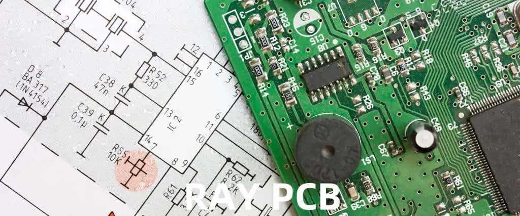
In the world of electronics manufacturing, two critical concepts often come into play: Design for Manufacturing (DFM) for Printed Circuit Boards (PCBs) and Design for Assembly (DFA) for Printed Circuit Board Assemblies (PCBAs). While these terms may sound similar, they serve different purposes and occur at different stages of the production process. This article will delve into the nuances of DFM PCB and DFA PCBA, exploring their differences, importance, and how they contribute to creating efficient, cost-effective, and high-quality electronic products.

Understanding DFM PCB
What is DFM PCB?
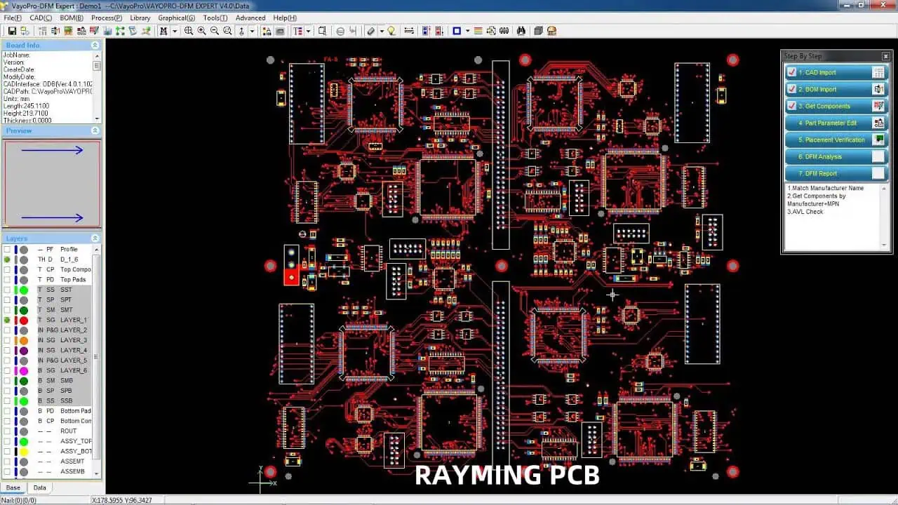
Design for Manufacturing (DFM) for Printed Circuit Boards is a methodology that focuses on optimizing the design of a PCB to ensure it can be manufactured efficiently, reliably, and cost-effectively. DFM PCB considers various factors that can affect the manufacturing process, such as material selection, component placement, trace routing, and manufacturing tolerances.
Key Objectives of DFM PCB
The primary goals of implementing DFM PCB include:
- Minimizing manufacturing defects
- Reducing production costs
- Improving yield rates
- Enhancing overall product quality
- Streamlining the manufacturing process
DFM PCB Considerations
When implementing DFM PCB, designers and engineers must take into account several crucial factors:
1. Material Selection
Choosing the right PCB material is critical for ensuring the board’s performance, durability, and manufacturability. Factors to consider include:
- Dielectric constant
- Thermal conductivity
- Coefficient of thermal expansion
- Cost
- Availability
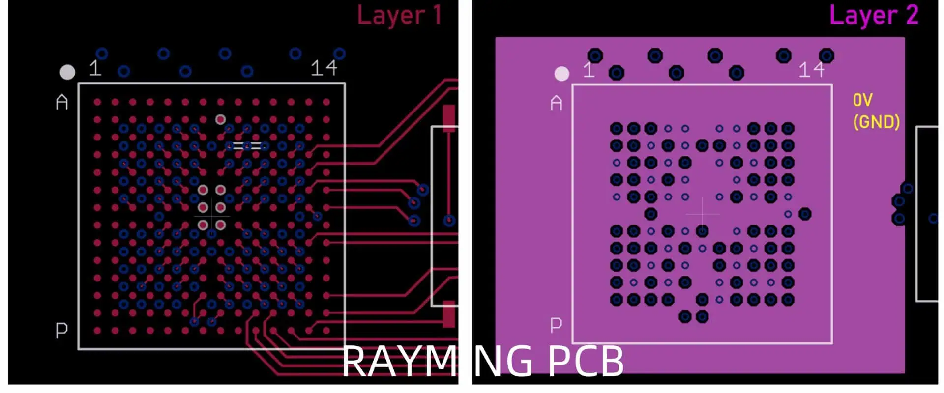
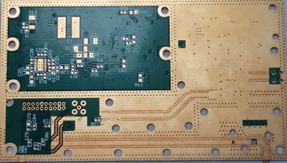
2. Layer Stack-up
The layer stack-up of a PCB affects its electrical performance, thermal management, and manufacturability. Key considerations include:
- Number of layers
- Layer thickness
- Copper weight
- Prepreg and core materials
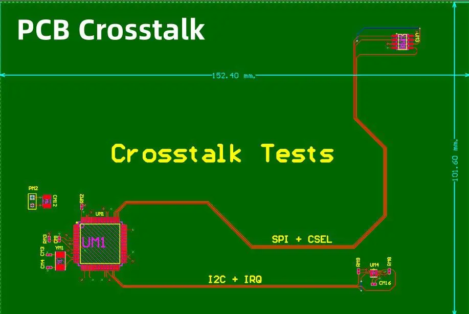
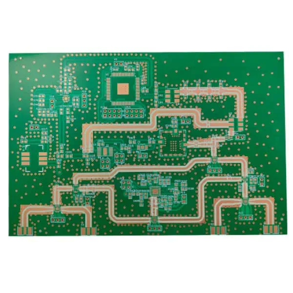
3. Trace Routing and Spacing
Proper trace routing and spacing are essential for maintaining signal integrity and preventing manufacturing issues. DFM PCB guidelines typically address:
- Minimum trace width and spacing
- Differential pair routing
- Controlled impedance requirements
- Via usage and placement
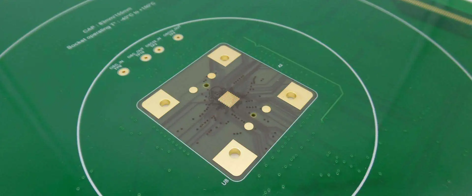
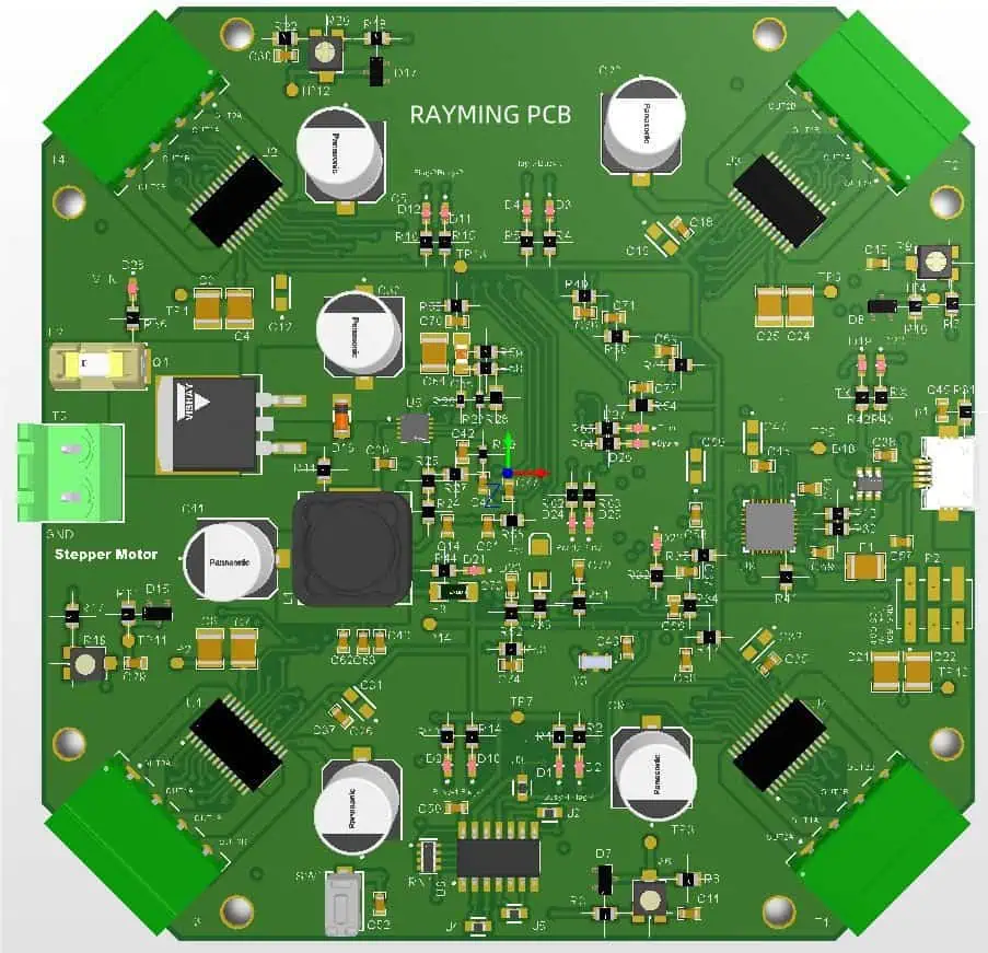
4. Component Placement
Optimizing component placement can significantly impact the manufacturing process. Consider:
- Component orientation
- Spacing between components
- Thermal relief for large components
- Accessibility for automated assembly equipment
5. Manufacturing Tolerances
Accounting for manufacturing tolerances is crucial to ensure consistent production quality. This includes:
- Drill tolerances
- Etching tolerances
- Solder mask tolerances
- Silkscreen tolerances
Benefits of DFM PCB

Implementing DFM PCB practices offers several advantages:
- Reduced manufacturing costs
- Improved product reliability
- Faster time-to-market
- Enhanced product quality
- Increased yield rates
- Simplified troubleshooting and rework
Understanding DFA PCBA
What is DFA PCBA?
Design for Assembly (DFA) for Printed Circuit Board Assemblies focuses on optimizing the design of a PCB and its components to facilitate efficient and cost-effective assembly processes. DFA PCBA aims to streamline the assembly process, reduce errors, and minimize production time and costs.
Key Objectives of DFA PCBA
The primary goals of implementing DFA PCBA include:
- Simplifying the assembly process
- Reducing assembly time and labor costs
- Minimizing assembly errors and defects
- Improving overall product quality
- Enhancing production efficiency
DFA PCBA Considerations
When implementing DFA PCBA, designers and engineers must consider several important factors:
1. Component Selection
Choosing the right components can significantly impact the assembly process. Consider:
- Component availability and lead times
- Package types and sizes
- Compatibility with automated assembly equipment
- Standardization of components
2. Component Placement and Orientation
Optimizing component placement and orientation is crucial for efficient assembly. Key considerations include:
- Consistent component orientation
- Adequate spacing for pick-and-place machines
- Grouping similar components
- Avoiding shadowing effects during soldering
3. Solder Joint Design
Proper solder joint design is essential for reliable connections and efficient assembly. Consider:
- Pad size and shape
- Solder mask clearances
- Thermal relief for large components
- Via-in-pad design (when necessary)
4. Test Point Access
Designing for testability is an important aspect of DFA PCBA. Consider:
- Adequate test point coverage
- Accessibility for probes and test fixtures
- Compatibility with automated test equipment
5. Panelization
Efficient panelization can significantly improve assembly throughput. Consider:
- Panel size and shape
- Fiducial marks for automated assembly
- Break-away tabs or V-score lines
- Tooling holes for fixturing
Benefits of DFA PCBA
Implementing DFA PCBA practices offers several advantages:
- Reduced assembly time and costs
- Improved product quality and reliability
- Enhanced manufacturing flexibility
- Simplified rework and repair processes
- Increased production throughput
- Reduced inventory and component management complexity
Comparing DFM PCB and DFA PCBA
While DFM PCB and DFA PCBA are closely related, they focus on different aspects of the production process. Let’s compare these two methodologies:
| Aspect | DFM PCB | DFA PCBA |
| Primary Focus | PCB manufacturing process | PCBA assembly process |
| Stage of Implementation | PCB design phase | PCBA design and component selection phase |
| Key Considerations | Material selection, layer stack-up, trace routing, manufacturing tolerances | Component selection, placement, solder joint design, testability |
| Main Goals | Optimize PCB manufacturability, reduce defects, improve yield | Streamline assembly process, reduce errors, minimize production time |
| Impact on Costs | Reduces PCB manufacturing costs | Reduces PCBA assembly and labor costs |
| Typical Stakeholders | PCB designers, manufacturing engineers |
Integrating DFM PCB and DFA PCBA
While DFM PCB and DFA PCBA focus on different aspects of the production process, they are not mutually exclusive. In fact, integrating both methodologies can lead to even greater improvements in overall product quality, cost-effectiveness, and manufacturing efficiency.
Benefits of Integration
- Holistic design approach
- Reduced overall production costs
- Improved product reliability and quality
- Faster time-to-market
- Enhanced manufacturing flexibility
- Simplified supply chain management
Strategies for Integration
To effectively integrate DFM PCB and DFA PCBA, consider the following strategies:
1. Cross-functional Collaboration
Encourage collaboration between PCB designers, PCBA designers, manufacturing engineers, and assembly engineers throughout the design process. This ensures that both DFM and DFA considerations are addressed from the early stages of product development.
2. Unified Design Guidelines
Develop a comprehensive set of design guidelines that incorporate both DFM PCB and DFA PCBA principles. This helps ensure consistency across all aspects of the design process.
3. Simulation and Analysis Tools
Utilize advanced simulation and analysis tools that can evaluate both PCB manufacturability and PCBA assembly processes. This allows for early identification and resolution of potential issues.
4. Design Reviews
Conduct regular design reviews that include stakeholders from both PCB manufacturing and PCBA assembly teams. This helps identify potential conflicts between DFM and DFA requirements and allows for timely resolution.
5. Continuous Improvement
Implement a feedback loop between design, manufacturing, and assembly teams to continuously refine and improve DFM PCB and DFA PCBA practices based on real-world production experiences.
Best Practices for Implementing DFM PCB and DFA PCBA
To maximize the benefits of both DFM PCB and DFA PCBA, consider the following best practices:
- Start early: Implement DFM and DFA principles from the beginning of the design process.
- Use standardized components: Whenever possible, use standard component packages and footprints to simplify both manufacturing and assembly.
- Design for testability: Incorporate features that facilitate both in-circuit and functional testing.
- Optimize for automation: Design PCBs and PCBAs with automated manufacturing and assembly processes in mind.
- Consider thermal management: Address thermal considerations in both PCB design and component selection to ensure reliable operation.
- Document thoroughly: Maintain detailed documentation of design decisions, manufacturing requirements, and assembly instructions.
- Stay up-to-date: Keep abreast of the latest manufacturing and assembly technologies to leverage new opportunities for optimization.
Conclusion
Understanding the differences between DFM PCB and DFA PCBA is crucial for anyone involved in the design and production of electronic products. While DFM PCB focuses on optimizing the manufacturability of the bare PCB, DFA PCBA concentrates on streamlining the assembly process of the completed board.
By implementing both methodologies and integrating them effectively, companies can achieve significant improvements in product quality, manufacturing efficiency, and overall cost-effectiveness. As the electronics industry continues to evolve, embracing these design philosophies will be essential for staying competitive and meeting the ever-increasing demands of modern technology.
FAQ
1. What is the main difference between DFM PCB and DFA PCBA?
The main difference lies in their focus: DFM PCB concentrates on optimizing the bare PCB manufacturing process, while DFA PCBA focuses on streamlining the assembly process of components onto the PCB.
2. Can DFM PCB and DFA PCBA be implemented independently?
While they can be implemented independently, integrating both methodologies typically leads to better overall results in terms of product quality, cost-effectiveness, and manufacturing efficiency.
3. How do DFM PCB and DFA PCBA impact production costs?
DFM PCB primarily reduces PCB manufacturing costs by optimizing the board design for efficient production. DFA PCBA reduces assembly and labor costs by streamlining the component placement and soldering processes.
4. At what stage of product development should DFM PCB and DFA PCBA be considered?
Ideally, both DFM PCB and DFA PCBA should be considered from the early stages of product development. Implementing these methodologies early in the design process can prevent costly redesigns and manufacturing issues later on.
5. How can companies ensure successful implementation of both DFM PCB and DFA PCBA?
Successful implementation can be achieved through cross-functional collaboration, unified design guidelines, use of advanced simulation tools, regular design reviews, and a commitment to continuous improvement based on feedback from manufacturing and assembly processes.