Breakout boards are essential tools in electronics prototyping and development. They provide a convenient way to access and utilize the features of complex integrated circuits (ICs) or modules by breaking out their pins into more manageable, breadboard-friendly formats. Designing a breakout board requires careful consideration of various factors, from component selection to PCB layout. This comprehensive guide will walk you through the process of designing a breakout board, covering everything from initial planning to final production.
Understanding Breakout Boards
What is a Breakout Board?
A breakout board is a printed circuit board (PCB) that “breaks out” the pins or connections of an electronic component into a more accessible format. These boards are particularly useful for working with surface-mount devices (SMDs), ball grid array (BGA) packages, or other components that are not easily breadboard-compatible.
Why Use Breakout Boards?
Breakout boards offer several advantages:
- Ease of prototyping board
- Improved accessibility to complex components
- Protection for sensitive ICs
- Simplified testing and debugging
- Cost-effective development process

Planning Your Breakout Board
Identifying the Target Component
The first step in designing a breakout board is to identify the component you want to break out. This could be:
- A microcontroller
- A sensor
- A communication module
- A power management IC
- Any other specialized component
Gathering Technical Information
Once you’ve identified the target component, gather all relevant technical information:
- Datasheet
- Application notes
- Reference designs
- Errata sheets
Defining Board Requirements
Based on the component specifications and your project needs, define the requirements for your breakout board:
- Power supply requirements
- Signal levels
- Communication interfaces
- Physical dimensions
- Environmental considerations (temperature, humidity, etc.)
Schematic Design

Choosing Additional Components
Select any additional components required for your breakout board:
- Voltage regulators
- Level shifters
- Passive components (resistors, capacitors, inductors)
- Connectors
- LEDs for status indication
Creating the Schematic
Using electronic design automation (EDA) software, create a schematic diagram of your breakout board:
- Place the main component symbol
- Add power supply circuitry
- Include necessary passive components
- Add connectors for external interfaces
- Implement any additional functionality (e.g., programming headers)
Design Considerations
When designing your schematic, keep these factors in mind:
- Signal integrity
- Power distribution
- Thermal management
- Electromagnetic compatibility (EMC)
- Testability and debugging access
PCB Layout
Choosing PCB Parameters
Determine the physical characteristics of your PCB:
- Board dimensions
- Number of layers
- Copper weight
- Material (e.g., FR-4, Rogers)
- Finish (e.g., HASL, ENIG)
Component Placement
Carefully place components on the PCB:
- Position the main IC
- Arrange supporting components logically
- Group related functions together
- Consider thermal requirements
- Ensure accessibility for probing and testing
Routing Considerations
When routing traces on your PCB, follow these guidelines:
- Use appropriate trace widths based on current requirements
- Maintain consistent impedance for high-speed signals
- Minimize signal path lengths
- Avoid right-angle turns in traces
- Use ground planes for improved signal integrity
- Implement proper power distribution
Design for Manufacturing (DFM)
Ensure your design is manufacturable by following DFM guidelines:
- Adhere to minimum trace width and spacing rules
- Maintain sufficient clearance between components
- Use standard drill sizes
- Include fiducial markers for assembly
- Add silkscreen labels for component identification
Design Verification

Electrical Rule Check (ERC)
Run an ERC to identify potential electrical issues:
- Unconnected pins
- Power supply conflicts
- Signal level mismatches
Design Rule Check (DRC)
Perform a DRC to catch layout violations:
- Trace width and spacing violations
- Clearance issues
- Drill size errors
- Copper pour problems
Manual Review
Carefully review your design:
- Check component footprints against datasheets
- Verify pin assignments and connections
- Ensure proper labeling and silkscreen information
- Review power and ground connections
Prototyping and Testing
Ordering PCB Prototypes
Choose a PCB manufacturer and order prototypes:
- Generate Gerber files from your design
- Select appropriate manufacturing options
- Order a small quantity for initial testing
Assembly
Assemble your prototype breakout boards:
- Use proper soldering techniques
- Follow ESD precautions
- Inspect for solder bridges or other defects
Functional Testing
Perform comprehensive testing of your assembled breakout board:
- Power-on test
- Voltage measurements
- Signal integrity verification
- Functional testing of all features
- Environmental testing (if applicable)
Design Iteration and Optimization
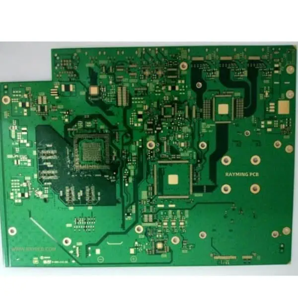
RAYMING 10 Layer Shengyi S1141 Intelligent Medical PCB
Product name: 10-layer intelligent medical PCB boards Board Material: S1141 Thickness: 1.2mm Layer Number:10 layers PCB Minimum line width/spacing: 4/4mil Finished product copper thickness: inner layer 1OZ, outer layer 1OZ Acceptance standard: IPC6012 CLASS 3 level Surface technology: immersion gold Dielectric constant: 4.4 Loss factor: 0.013 Application: Medical equipment
Analyzing Test Results
Review the results of your prototype testing:
- Identify any issues or failures
- Assess performance against requirements
- Gather feedback from users (if applicable)
Design Refinement
Based on your analysis, refine your design:
- Correct any errors or oversights
- Optimize component placement and routing
- Improve thermal management if necessary
- Enhance labeling and documentation
Performance Optimization
Fine-tune your design for optimal performance:
- Reduce noise and interference
- Improve power efficiency
- Enhance signal integrity
- Optimize for size or cost, if needed
Documentation
Creating Design Files
Prepare comprehensive design files:
- Schematic diagram
- PCB layout files
- Bill of Materials (BOM)
- Assembly drawings
- 3D models (if applicable)
Writing User Documentation
Develop clear and concise user documentation:
- Overview of the breakout board
- Pin descriptions and functions
- Electrical specifications
- Usage instructions
- Example applications or code snippets
Production and Quality Control

Scaling Up Production
When moving to larger-scale production:
- Review and optimize your design for volume manufacturing
- Consider panelization for efficient PCB production
- Develop a test plan for quality assurance
Quality Control Measures
Implement quality control procedures:
- Incoming component inspection
- Automated optical inspection (AOI) during assembly
- In-circuit testing (ICT) or functional testing
- Statistical process control (SPC) for ongoing quality monitoring
Advanced Considerations
High-Speed Design Techniques
For breakout boards with high-speed signals:
- Implement controlled impedance routing
- Use proper termination techniques
- Consider signal integrity simulations
RF Considerations
When designing breakout boards for RF components:
- Use appropriate RF PCB materials
- Implement proper grounding techniques
- Consider shielding requirements
Thermal Management
For components with significant heat dissipation:
- Use thermal vias to improve heat transfer
- Consider adding heatsinks or cooling solutions
- Perform thermal simulations if necessary
Comparison of Breakout Board Design Approaches
| Aspect | Simple Breakout | Advanced Breakout | Modular Breakout |
| Complexity | Low | High | Medium |
| Flexibility | Limited | Extensive | Moderate |
| Cost | Low | High | Medium |
| Development Time | Short | Long | Medium |
| Customization | Minimal | Extensive | Moderate |
| Typical Applications | Basic prototyping | High-performance systems | Versatile development |
| Skill Level Required | Beginner | Expert | Intermediate |
Frequently Asked Questions (FAQ)
1. What software should I use to design a breakout board?
There are several options for PCB design software, ranging from free to professional-grade tools. Popular choices include:
- KiCad (free and open-source)
- Eagle (free for hobbyists, paid for professional use)
- Altium Designer (professional-grade, paid)
- Fusion 360 Electronics (cloud-based, subscription model)
Choose a tool that fits your budget and skill level, and offers the features you need for your specific project.
2. How do I determine the appropriate trace width for my breakout board?
Trace width depends on several factors, primarily the current carrying capacity and the available space on the PCB. You can use online trace width calculators or consult PCB design guidelines to determine the appropriate width. As a general rule:
- For signal traces, a width of 8-10 mils (0.2-0.25 mm) is often sufficient.
- For power traces, calculate the width based on the maximum current and allowable temperature rise.
- Always consult your PCB manufacturer’s capabilities and design rules.
3. How can I protect sensitive components on my breakout board?
To protect sensitive components:
- Use proper ESD protection circuits
- Implement reverse polarity protection for power inputs
- Add buffer circuits for I/O lines if necessary
- Consider conformal coating for environmental protection
- Use proper grounding techniques to minimize noise and interference
4. What are some common mistakes to avoid when designing a breakout board?
Common mistakes include:
- Incorrect footprints or pinouts
- Inadequate power distribution
- Ignoring signal integrity for high-speed designs
- Poor component placement leading to difficult assembly or testing
- Neglecting thermal considerations for power-hungry components
Always double-check your design against component datasheets and follow best practices for PCB design to avoid these issues.
5. How can I reduce the cost of my breakout board design?
To reduce costs:
- Optimize the board size to minimize material usage
- Use standard components instead of specialized ones where possible
- Consider two-layer boards instead of multi-layer designs for simpler circuits
- Design for standard manufacturing processes to avoid special requirements
- Order PCBs in larger quantities to benefit from volume discounts
Remember that cutting costs shouldn’t compromise the functionality or reliability of your breakout board. Always balance cost reduction with performance and quality requirements.

